ece 4502 mixed-signal integrated circuit designstevo.bailey/documents/micreport.pdfintegrated...
TRANSCRIPT
1
May 9th
, 2011
ECE 4502 – Mixed-Signal Integrated Circuit Design
Chas DeVeas
Anisha Gorur
Christian Viehland
Stevo Bailey

2
Abstract This report presents the design and simulation of a mix signal circuit to process the
output of a moisture sensor. The moisture sensor is a capacitor bridge, where one of the branches
varies with moisture. Included in the circuit are a common mode feedback differential amplifier,
a double balance mixer, a low pass filter, difference amplifier, and a SAR ADC. We present the
design, tradeoffs, and final performance of our circuit as well as considerations on market size
and impact on society.
Introduction
Since the dawn of digital electronics, the world of technology has been moving further
away from analog circuitry and more towards the benefits associated with digital
implementation. Compared to an analog signal, which has a continuous and infinite number of
states, a digital signal has a finite number of discrete values and is much easier to store
compactly and communicate without noise interference. Another benefit of using digital signals
and circuitry is that it can be manipulated easily with computers, arguably the most prominent
tool used by humans today.
Take a song, for example. If a song was stored as an analog signal on a music record, a
user interested in hearing or manipulating the song has only one way to do it- by using a record
player. Now, if another user had this same song stored digitally, he or she could copy it to a
computer in just a few seconds, manipulate it in one of thousands of computer programs, alter it
in any way he or she chose, and save it as another song. The second user could email the song to
a friend, or upload it to a music player the size of his or her thumb. In addition, while the first
user could listen to his or her record many times, eventually it would break and the information
would be lost forever (and even before that the information would be corrupted noticeably). The
second user, on the other hand, would be long outlived by the same exact digital information that
he or she started with. It is clear to see how supremely useful digital information can be when
compared to analog information. Of course, the digital version of the song did not come from a
band in a music studio shouting a string of ones and zeros into microphones. It started with
human voice, vibrating strings, and banging drums; it started with analog.
In order to obtain a digital signal—and all the benefits associated with it—one must turn
an analog signal into discrete values that can be quantified into bits. For an electronic circuit, this
means having a component that changes continuously in response to an analog signal and
propagates that information through several stages, resulting in discrete, digital bits (ones and
zeros). Circuits which are manufactured on silicon and which accomplish this task are called
mixed-signal integrated circuits. Almost all of today's modern devices make use of mixed-signal
integrated circuits to accomplish tasks such as transmitting speech across cellular networks,
detecting changes in temperature in a computer, and taking digital photographs. Because the
electronics are so small
The purpose of this project is to design and simulate a mixed-signal integrated circuit that
can detect moisture changes when buried underground. The specific applications of this are
explored in more detail in the market analysis, but in general there is a need for some people and
organizations to monitor large plots of land which are sensitive to moisture. A network of
sensors like this could provide a digital look into the state of moisture on a large area of land.
The small changes in moisture can be thought of as an analog signal that changes the value on a
small variable capacitor. This component of the circuit then acts as the stimulus which
propagates that signal through the several stages of the circuit and produces digital information at

3
the end. This report details the approach, market analysis, design, testing approach, and
simulation of the mixed-signal moisture sensor. The general approach of the design is clearly
outlined in text and then shown in a block diagram, with the specific components each
constructed and simulated using Cadence simulation software. A testing approach is then
recommended for verification of the circuit during the manufacturing process to ensure that each
group of electronic components on the silicon wafers is functioning correctly. Finally, the results
of the project are presented and conclusions are drawn.
Market Analysis A moisture sensor based off of this circuit could serve numerous purposes across a
variety of customers. Specifically, farmers with large plots of land and crops sensitive to
moisture variations could install a large network of these sensors in order to monitor the moisture
on their property. It is well documented that optimizing the water intake for crops increases
yield—soil moisture sensors can reduce water usage from at least 5% up to 88%.i Also,
researchers monitoring a specific region of land for its moisture or conducting experiments could
also be a potential customer.
According to the Department of Agriculture, there are roughly 938 million acres of
farmland in the United Statesii. Assuming a conservative estimate of .1% of that farmland
belongs to farmers who would be interested in using the device, the market for the device would
cover 938 thousand acres. Usage per farmer may vary, but we can assume again that a farmer
would use one device per acre resulting in nine million devices sold. If a single sensor were sold
at even $20 (on the cheaper side, as prices range from $15- $1500 USD), the income from this
sensor would be in the range of $18.8 million.
We predict that the potential for researchers as a customer would be much smaller; the
number of researchers working with agriculture is only a fraction of the farmers. There are
probably only a handful of studies that would need widespread use of moisture sensors, resulting
in a number of purchases from the hundreds to possibly the thousands—insignificant when
compared to the market from farmers.
Societal Impact
A circuit that measures soil moisture, whether it can be considered a good thing or a bad
thing, does not drastically impact human society as a whole. While it should help to increase
crop yield and control irrigation for farmers, and possibly contribute to humanity's collective
knowledge through research, there most likely will not be any outstanding implications that this
circuit will have. Below is a brief inspection of the ethical, health, and safety concerns, as well as
commentary on societal implications of the product.
There should not be any direct negative drawbacks to introducing this technology into the
world, and unless it fails to do its job, it should only contribute to the human condition. In fact,
from an ethical standpoint, this product should be completely sound. It is likely that the worst-
case scenario that could arise from this product is that a farmer plants 50 of these into his land
only to find that the sensors failed for some reason. As for health risks, the potential impact of
even a large network of these sensors in a plot of farmland should be minimal. There are no
dangerous materials or components used to manufacture the product which could somehow leak
into the food supply, and the operation and installation of the sensors poses minimal risk for the

4
person doing so. It is this company's opinion that this product is a low-risk, high-reward tool.
Admittedly, as far as overall impact on society, the circuit will not cause any major
waves. It was conceived in order to meet a human need that was large enough to yield a potential
profit. Although most likely minimally, the ways in which it could affect society include
influencing food prices and farming practices. If farmers were able to use this product to (in an
extreme case) increase their output by 50%, that would most likely increase the supply of their
food produce and cause a reduction in price for that food item. If other farmers caught wind of
success like that and emulated that process, the nationwide economy could see a change resulting
from this product. In addition, that could further develop the relationship between agriculture and
technology. Ultimately, this product could greatly develop the presence of sensor networks in
agriculture practices. In the future, farmers may even be able to check the detailed status of every
living cell on their land, and this product could have helped grandfather such a system into
existence. This is not the first sensor that would be used on farmland, but it could help spread
their popularity amongst farmers.
The most direct impact that this product should have is with the controlled use of water
used by farmers. A farmer using a system of these sensors could find that he or she is under-
watering or over-watering specific portions of land. As stated above, over-watering can account
for even up to 50% of the water use on some plots of land. This circuit will help farmers better
choose where to distribute their water—especially in arid and drier areas where watering is most
necessary. This sensor should reduce wasted water, which will conserve both funds for farmers
and the environment as a whole.
While this product will not save the world or pose any extreme threat to mankind, it will
potentially fill a very small niche in the agriculture world, save some water in the long run,
enable greater crop yields, and enhance this company’s yearly profits.
Design Approach
A brainstorming session began the project. After throwing around different analog
sensors and possible uses, it was decided that a moisture sensor and a soil pH sensor in a cheap
product could allow farmers to measure data on their crops' soil. Next, a basic block diagram of
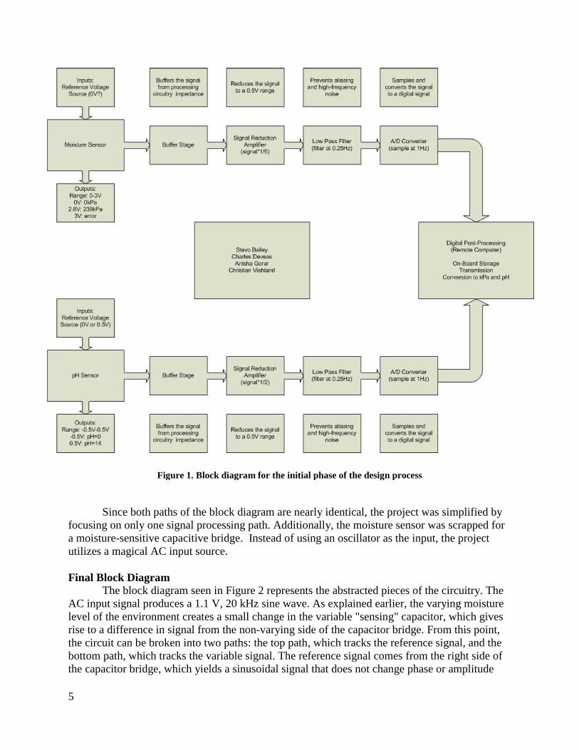
the system was drawn up. This block diagram in Figure 1 shows top-level details about the
various stages of data collection and processing. Each sensor needs an input reference voltage,
and each one has an output voltage which varies with the measured property. These input and
output data were found online for commercial sensors. A buffer stage is needed to protect the
signal from low-impedance loads. An amplifier then reduces the voltage to an acceptable range
for the A/D converter, and the signal is finally filtered and converted. Once digital, the data are
sent to a remote computer, which decodes it into usable information and stores it. One benefit to
using this design was that both stages are relatively similar, so once one was completed the other
could be easily created from the first.
5
Since both paths of the block diagram are nearly identical, the project was simplified by
focusing on only one signal processing path. Additionally, the moisture sensor was scrapped for
a moisture-sensitive capacitive bridge. Instead of using an oscillator as the input, the project
utilizes a magical AC input source.
Final Block Diagram The block diagram seen in Figure 2 represents the abstracted pieces of the circuitry. The
AC input signal produces a 1.1 V, 20 kHz sine wave. As explained earlier, the varying moisture
level of the environment creates a small change in the variable "sensing" capacitor, which gives
rise to a difference in signal from the non-varying side of the capacitor bridge. From this point,
the circuit can be broken into two paths: the top path, which tracks the reference signal, and the
bottom path, which tracks the variable signal. The reference signal comes from the right side of
the capacitor bridge, which yields a sinusoidal signal that does not change phase or amplitude
Figure 1. Block diagram for the initial phase of the design process

6
with moisture. The variable signal comes from the left side of the bridge, and varies in amplitude
(and slightly in phase) due to the varying capacitance of the ―Sensing Capacitor.‖ Next, both
signals are passed through several unity gain buffers (fed with two different DC common mode
reference signals) and then fed into two separate mixers. The mixers take the differential output
of the buffers and multiply the two differential signals together. The top mixer multiplies the
variable signal with itself, while the bottom mixer multiplies the variable signal with the
reference signal. Since the input signals have the same frequency, the output of the mixers is a
DC signal with a 40 kHz AC component on top of it. The low pass filters remove the AC
component, leaving just the DC signals. At this point, the two DC signals (one variable and one
reference) are subtracted via a difference amplifier, resulting in a DC signal with a voltage that
depends linearly on the moisture in the sensing capacitor.
AC Input
Capacitor Bridge
Sensing Capacitor
Differential Amplifiers
+
–
+
–
+
–
Vcm
Vcm
Common Mode
FeedbackMixer
Mixer LPF
LPF
+
–
ADC
Difference AmplifierMixing and Filtering
Figure 2. The final block diagram
Test Plan:
A test plan can systematically bring a user who is unfamiliar with the inner workings of a chip, to a
conclusion about what is and is not working inside the chip. To test this circuit for manufacturing, insert
analog multiplexors before and after the individual block-level components of the circuit. These
multiplexors would have pins accessible during the manufacturing process which would allow probes to
activate the particular components as needed. Following are some specific recommendations for testing
the individual components.

7
Component Recommended Inputs Expected Output Comments
Capacitor Bridge Sine wave across cap
bridge.
Sine wave of reduced
amplitude.
Differential Amplifiers Sine wave at a known
amplitude centered at
550 mV.
Sine wave of the same
frequency with some
gain.
The gain is variable here
based on the common
mode feedback.
Mixers Two sine waves at 20
kHz.
Single sine wave at 40
kHz.
Low Pass Filter Sine wave at 40 kHz. DC signal of the
original sine wave.
Some oscillations occur
initially, but settle.
Difference Amplifier DC signal at 300 mV to
inverting input.
DC signal at 250 mV to
non-inverting input.
DC signal at 350 mV The output of the
difference amp should
be the difference of the
inputs plus 300 mV.
Differential Amplifier with Common Mode Feedback
[groupX/christian/cvdiffamp/final]
This is a differential pair with as second differential pair, common mode feedback
amplifier (CMFA), that provide feedback to set the common mode out the differential output.
The two resistors on the input to the CMFA average Vout+ and Vout-, and allow the average to be
compared to Vcm. The output of the CMFA is fed back to the gate of the NMOS current source of
the first differential pair. This causes the current source to sink enough current to set the drain
voltage of the differential pair to Vcm (figure 1). There are several design considerations in this
stage. First we need the gain to be low (around one). In the initial layout the input to the CMFA
was split onto two transistors that were half the original width (figure 2). However the gain of the
differential pair was too high even after modifying the lengths and the widths of the transistors
(around 100 V/V). Furthermore this topology has limited output range, the sine wave is distorted
if the output amplitude is above 5 mV (figure 3a), due to incorrect balancing when the input to
the common mode feedback amplifier swings too far away from desired common-mode voltage.
In order to use this topology, our input sine wave would have to be 100uV. Using a signal this
small would be impractical as it would make measuring changes in capacitance hard to measure.
Using the resistors on the input to the CMFA allow the differential amplifier to function over a
larger output range (figure 3b) and reduces the gain (reduces the resistance looking out of the
differential pair). Since the outputs are sine waves that are 180 degrees out of phase, the average
is just the common mode of the two signals. This prevents the input voltage to the common mode
feedback amplifier from swinging too far away from the common mode voltage. However, this
comes at the cost of increased area on chip (the resistors could be implemented with transistors)
and increased power dissipation. However it makes it easy to modify the gain of the circuit. A
draw back to CMFA implementation of a differential amplifier with common mode feedback is
that the gain changes for different common mode voltages. As the desired common mode

8
becomes lower, the common mode feedback causes the current source of the differential pair to
sink more current. In effect raises the trans-conductance of the differential pair, which increases
the gain. Our application requires signals at 600 and 850 mv, which would have different
amplitude. However, since the signals will be multiplied together this can be corrected for during
digital processing. Finally a small amount of capacitance was added to ensure stability. Since
the circuit was stable at 20kHz, the only frequency in use, no further stability analysis was
performed. This amplifier preforms very well. There is only one millivolt of offset from the
desired common mode, and the sine wave is undistorted (figures 4a and 4b).
Differential Amplifier Offset Correction
The feedback between the differential pair and the CMFA could be disconnected, and
two amplifiers could offset corrected independently. However, the implementation of the control
logic and the offset correction for this scheme proved problematic and is not included in the final
layout. Monte Carlo simulations show that this common mode feedback amplifier will not
function in the circuit without offset correction (figure 5).

9
(Figure 3: Final schematic for differential amplifier with common mode feedback)
(Figure 4: Initial schematic for differential amplifier with common mode feedback)

10
(Figures 5 a and b: a, distorted output from original layout (50 mV amplitude). b, undistorted
output from final layout (100 mV amplitude)
(Figures 6 a and b. Output for 650 mV (a) and 800 mV (b) and common mode)
(Figure 7: Monte Carlo simulation)
11
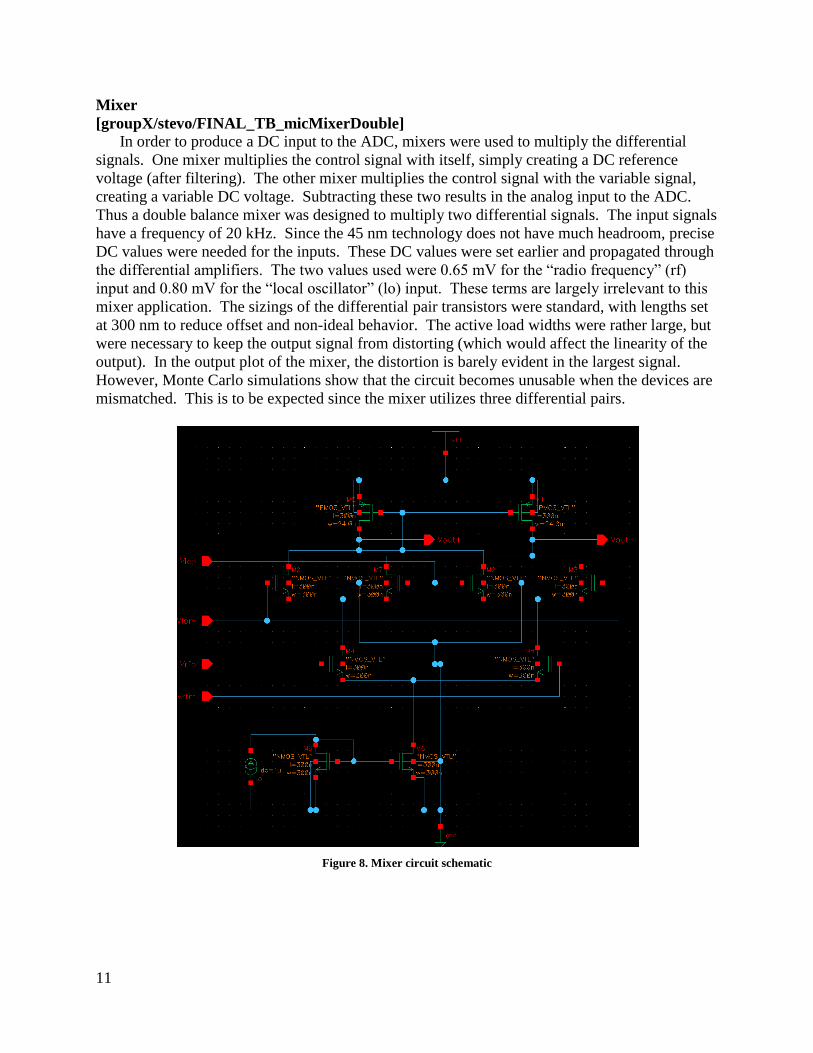
Mixer
[groupX/stevo/FINAL_TB_micMixerDouble]
In order to produce a DC input to the ADC, mixers were used to multiply the differential
signals. One mixer multiplies the control signal with itself, simply creating a DC reference
voltage (after filtering). The other mixer multiplies the control signal with the variable signal,
creating a variable DC voltage. Subtracting these two results in the analog input to the ADC.
Thus a double balance mixer was designed to multiply two differential signals. The input signals
have a frequency of 20 kHz. Since the 45 nm technology does not have much headroom, precise
DC values were needed for the inputs. These DC values were set earlier and propagated through
the differential amplifiers. The two values used were 0.65 mV for the ―radio frequency‖ (rf)
input and 0.80 mV for the ―local oscillator‖ (lo) input. These terms are largely irrelevant to this
mixer application. The sizings of the differential pair transistors were standard, with lengths set
at 300 nm to reduce offset and non-ideal behavior. The active load widths were rather large, but
were necessary to keep the output signal from distorting (which would affect the linearity of the
output). In the output plot of the mixer, the distortion is barely evident in the largest signal.
However, Monte Carlo simulations show that the circuit becomes unusable when the devices are
mismatched. This is to be expected since the mixer utilizes three differential pairs.
Figure 8. Mixer circuit schematic

12
Figure 9. The difference of the outputs of the mixer for various amplitudes of the lo input; after filtering, the DC output
will show a linear dependence on the amplitude of the lo input versus the amplitude of the rf input
Figure 10. Monte Carlo simulation of the output in Figure 2 with the largest amplitude; device mismatch makes the mixer
unusable
13
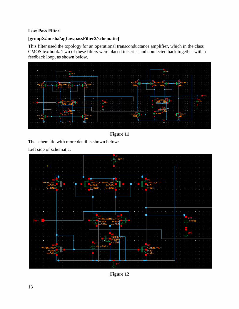
Low Pass Filter:
[groupX/anisha/agLowpassFilter2/schematic]
This filter used the topology for an operational transconductance amplifier, which in the class
CMOS textbook. Two of these filters were placed in series and connected back together with a
feedback loop, as shown below.
Figure 11
The schematic with more detail is shown below:
Left side of schematic:
Figure 12

14
Right Side of schematic
Figure 14
As you can see, the OTA is the same both times. To filter the signal, a 90pf capacitor on
the output of both OTAs was used. It considerably lowered the gmOTA as well. The output stage
of the circuit, (M7 and M3 on the left side of the circuit) had a much smaller w/l than the rest of
the circuit to lower gmOTA so that a small capacitor could be used to fit with the rest of the design
specifications so that it could fit on the ―chip‖ our team would manufacture. However, this most
likely made the schematic too sensitive to mismatch, because OTA’s become more stable as the
load capacitance increases. This was one of the biggest tradeoffs, however in the interest of time
I chose to keep the gmOTA of the circuit very small. Also, the bias voltage for M6 should be in a
biasing circuit, not a DC voltage, but there was not enough time to build one of these circuits.
For now, the vdc providing the bias works well. Below is the transient response of the circuit.
The output was centered around 500mV, which was correct for the input of 550mV with an
amplitude of .05V and a frequency of 40kHz. There were a few tradeoffs in this design, though
for the most part the low pass filter itself was relatively easy to build. Adding a second stage to
the low pass filter made the output more stable. Late into the low pass filter design, it was
discovered that a buffer was necessary on the output if the circuit was to drive something other
than a capacitive load. The team tried to build a buffer for hours, but in the end, it did not work
and in the final schematic, the buffer for the amplifier had to be abstracted out with a voltage
controlled voltage source.
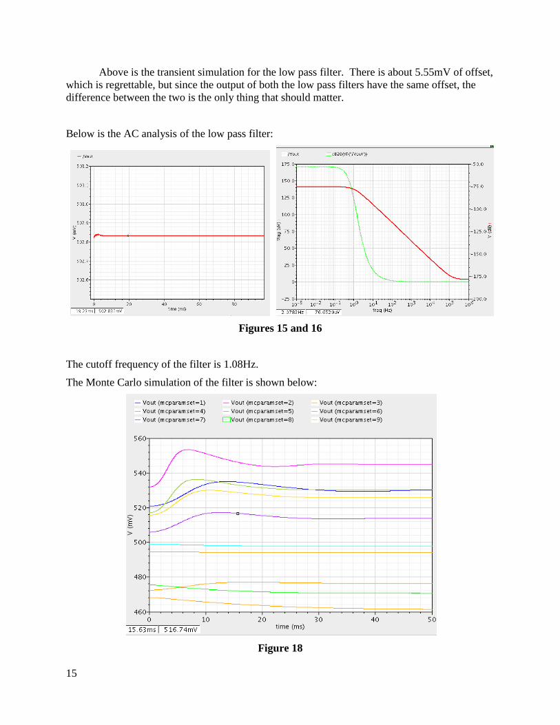
15
Above is the transient simulation for the low pass filter. There is about 5.55mV of offset,
which is regrettable, but since the output of both the low pass filters have the same offset, the
difference between the two is the only thing that should matter.
Below is the AC analysis of the low pass filter:
Figures 15 and 16
The cutoff frequency of the filter is 1.08Hz.
The Monte Carlo simulation of the filter is shown below:
Figure 18
16
Looking at the Monte Carlo simulation, the device is unusable. The output of the low
pass filter should be around 500mV, however with mismatch the output ranges from ~460mV to
555mV.
Difference Amplifier
[groupX/christian/diffamp1/schematic]
This portion of the circuit takes the outputs of the two Low Pass Filters and subtracts the
constant, DC ―control‖ signal from the DC ―variable‖ signal arising from the sensing capacitor.
This difference is what is ultimately fed into the AD converter to produce the digital
measurement.
The circuit is that of an operational amplifier, with feedback in the form of four resistors
(later to be replaced by FETs) to accomplish a differencing effect for the inputs Vpos and Vneg
(left and bottom). The formula for determining the output voltage of the difference amplifier
consists of the ratio of the two resistors multiplied by the difference between Vpos and Vneg. In
the schematic below, the resistors are all of equal value, and there is unity gain for the input
difference.
The left portion of the circuit consists of a differential pair, an active load, and a current
mirror. The gate of the left FET in the differential pair acts as the non-inverting input and is
connected to V1, and the gate of the right FET acts as the inverting input. The differential pair is
then followed by a gain stage and a buffer stage, with the output fed back to the inverting input.
It should be noted that the upper FET in the gain stage, above the diode-connected NMOS and
the current mirror, was doubled in width in order to account for the current that it draws. Since
the current mirror in this stage is identical to the current mirror below the differential pair, it
draws the same amount of current that goes through both of the 5 micrometer-wide FETs. Thus,
the width of this single FET had to be doubled. There is also a compensating capacitor (10 pF) in
place in order to make the op-amp stable. The diode-connected device beneath that common-
emitter stage is in place so that at least one of the voltages controlling the final buffer stage FETs
is in the active region. If that FET didn’t drop the voltage, then the output could be distorted if
both of the rightmost transistors weren’t operating in the active region.

17
Schematic:
Figure 19
Transient Simulation:
Figure 20

18
Figure 2 shows the results of sweeping the non-inverting input from 500 mV to 650 mV
with the inverting input set at 500 mV. These values were chosen since they are near the
expected range from the Low Pass Filters preceding this stage. As stated above, the expected
output of the difference amplifier is [Vout = Vpos – Vneg + 300 mV]. From this DC analysis,
the amplifier is true to this formula to within 1 mV.
Figure 21
This Monte Carlo analysis shows ten trials with varying offsets. The desired value is 340
mV, since the inputs into the difference amplifier were 560 mV and 520 mV (and the result
should be [V+ - V- + 0.3V]). In its current condition, without offset-correction, the output of this
difference amplifier would result in an inaccurate digital conversion. Since this output feeds
directly into the AD converter, the final digital value would be corrupted due to this error,
especially since it is accurate to eight bits. With offset correction implemented later on, this error
could be mitigated. In its current state, this would not pass for successful.
Analog-to-Digital Converter
[groupX/stevo/FINAL_TB_micADC]
The analog-to-digital converter (ADC) uses successive approximation to produce an 8-bit
digital output. An 8-bit shift register keeps track of which bit the comparator is comparing. It
starts at the MSB and proceeds through all the bits until the output is complete. All the bits are
zero except the current bit being compared. The successive approximation register (SAR)
produces the digital output. It starts at the MSB, making it equal to logical 1. Then its outputs
are fed into a digital-to-analog converter (DAC), which converts the data to an analog value

19
between 0.3 V and 1.1 V. The comparator uses this and the input to say whether the digital
output should be higher or lower. If higher, then the MSB is kept at one; if lower, the MSB
becomes zero. The shift register shifts over one bit, and the cycle repeats until all the bits have
been determined. The logic elements (registers, muxes, inverters, etc.) use minimum size
features and dual width sizing. The DAC and comparator had to be adjusted greatly to produce
an output with sufficient resolution.
The DAC uses charge scaling to produce an analog output. The charge scaling array was
split using another capacitor to reduce the sizes of the capacitors. Since the comparator’s
resolution diminished below 300 mV, the lower reference voltage of the DAC was 300 mV. The
upper reference voltage maxed out at 1.1 V since the comparator still produced accurate results
this high. It was discovered that the charge scaling capacitors were leaking one to two millivolts
during each clock cycle before being reset. The cause of this was the transmission gates in the
reset switches. These gates were minimum-sized, which let leakage through easily. Thus the
lengths of these transmission gates were increased, reducing the leakage to less than one
millivolt. Also, the DAC capacitors overshoot and undershoot the final value, but they settle
quickly enough that this non-ideality was ignored. These capacitors were made as big as
possible (with the largest being 16 pF) to improve accuracy and reduce charge leakage.
Working concurrently with the DAC, the comparator had to be very sensitive. Since the LSB
of the output changes every 0.8/28 = 3.125 mV, the comparator needs to have little to no
hysteresis and be able to detect 1-2 mV differences. A pre-amplifier stage introduces some gain
and allows faster speeds by not having any high-impedance nodes. The decision circuit uses
positive feedback to determine which signal is greater. In order to increase the sensitivity, these
transistors were made very small. To ensure very little hysteresis, they were all made the same
size. Finally, an amplification stage increases the output to VDD and ground (logical 1 and
zero). Three digital inverters introduce the regenerative property and buffer the output. This
comparator can differentiate signals within 1-2 mV of each other.
The ADC symbol requires the following inputs and performs the following operations. Vin
is the analog input signal, and it must be between 0.3 V and 1.1 V. The clock frequency should
be approximately 200 kHz. Reset performs asynchronous resets to the registers and discharges
the DAC capacitors. Typical errors are less than 1 %, with the error increasing slightly around
the minimum and maximum signal swing values. SARSet sets the value of the current SAR flip-
flop to logical one. The current SAR flip-flop is determined by the shifter register. Shift causes
a shift in the flop-flop values of the shift register, causing the ADC to compare the next bit.
ShiftIn is the input into the shift register, which gets loaded into the register’s MSB every time
Shift is called. An entire conversion from Vin to a digital signal takes approximately 100 μs, so
the ADC can read 10,000 samples per second.

20
Figure 22. The ADC circuit schematic

21
Figure 23. Part of the shift register circuit schematic
Figure 24. Part of the SAR circuit schematic

22
Figure 25. The DAC circuit schematic
Figure 26. ADC output bits 0-5 for input voltages of 1.088275 V (0-100μs) and 0.41555 V (100-200μs)
Figure 27. ADC output bits 2-7 for input voltages of 1.088275 V (0-100μs) and 0.41555 V (100-200μs); the final digital
outputs were 1111101 and 00100100

23
Overall Results
Figure 28
Conducting a parametric analysis of the overall circuit by varying the sensing capacitor
yielded the above output values at the analog end of the output. These signals are the result of the
amplifying, mixing, filtering, and differencing of the original signal taken off of the capacitor
bridge. As originally designed, the output of the circuit varies linearly with the sensing capacitor,
which is essential for the analog to digital conversion. In this figure, the maximum value
corresponds to 105 pF, the maximum possible value of the sensing capacitor, and the minimum
value corresponds to 100 pF, the minimum sensor value.

24
Final Monte Carlo Analysis
This Monte Carlo analysis of the full circuit shows that, without offset-correction, the
various internal components of the circuit and their internal mismatch causes the final DC value
to flip to the upper and lower rails of the final differencing amplifier. The total error due to offset
that propagates through the circuit is enough to bring the final voltages to the rails.
Digital Output
Four simulations were run. The sensing capacitor was set to a certain capacitance value,
corresponding to a moisture level. The output of the difference amplifier was recorded, and this
value was used as the input to the ADC. Since simulating both the signal processing path and the
ADC would take too long, they were done separately. he output of the processing path was
approximately constant, so the input to the ADC was a DC source with voltage shown in column
two. The output of the ADC is shown in column three (and converted to decimal in column
four). This value was used to calculate a capacitor value, shown in column five. The last column
shows the error between the calculated capacitor value and the actual capacitor value. As seen,
this error is relatively small, and probably well within any tolerance requested by a farmer.
Capacitor Value (Actual) ADC Input ADC Output (Bin) ADC Output (Dec) Capacitor Value (Calc) Error
101 pF 0.4310 V 00101111 47 100.9180 pF 0.08%
102 pF 0.5422 V 01100100 100 101.9531 pF 0.05%
103 pF 0.6543 V 10011010 154 103.0078 pF 0.01%
104.5 pF 0.8218 V 11101011 235 104.5898 pF 0.09%

25
Conclusion
Overall, the circuit was largely a success. An analog circuit was constructed that could
accurately read the value of a variable capacitor bridge in an alternating reference voltage. This
linearly-varying output was then calibrated across its entire range to an analog-to-digital
converter. The weaknesses of the circuit include offset correction, which was not implemented at
this point in time, the use of resistors in place of FETs in some components, and idealized
buffers after the LPFs. Given more time and resources, offset correction would be added to
mitigate the effects of natural offset in transistors, the idealized buffers would be replaced with
actual ones, and the resistors would be replaced with FETs. Barring these imperfections, though,
the circuit was a success and accomplished what its original purpose was. The results show that
the capacitor value was read to within 1% accuracy, which was then converted using a
successive approximation ADC to 8 bits of accuracy.
i http://buildgreen.ufl.edu/Fact_sheet_Soil_Moisture_Sensors.pdf
ii http://www.ers.usda.gov/statefacts/us.htm