ece 368: cad based logic design lecture notes # 1 ...dutt/courses/ece368/lect-notes/lect1... ·...
TRANSCRIPT

ECE 368: CAD Based Logic Design
Lecture Notes # 1
Introduction: Combinational Logic and Its DescriptionUsing Hardware Description Languages (HDLs)
SHANTANU DUTT
Department of Electrical and Computer EngineeringUniversity of Illinois, Chicago
Phone: (312) 355-1314; e-mail: [email protected]: http://www.ece.uic.edu/˜dutt
Shantanu Dutt UIC 1
1
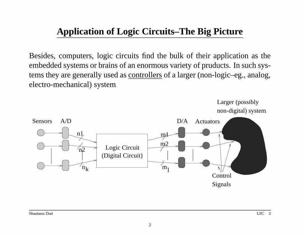
Application of Logic Circuits–The Big Picture
Besides, computers, logic circuits find the bulk of their application as theembedded systems or brains of an enormous variety of pruducts. In such sys-tems they are generally used as controllers of a larger (non-logic–eg., analog,electro-mechanical) system
non-digital) systemLarger (possibly
Logic Circuit(Digital Circuit)
nk ml
A/DSensors D/A
Control
Actuators
n1
n2
m1
m2
Signals
Shantanu Dutt UIC 2
2
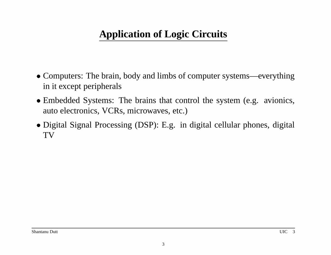
Application of Logic Circuits
� Computers: The brain, body and limbs of computer systems—everythingin it except peripherals
� Embedded Systems: The brains that control the system (e.g. avionics,auto electronics, VCRs, microwaves, etc.)
� Digital Signal Processing (DSP): E.g. in digital cellular phones, digitalTV
Shantanu Dutt UIC 3
3

Application of Logic Circuits (contd.)
� Logic Circuits are used to realize functions of the type:
If input condition C1 holds then do output actionA1
else if input condition C2 holds then do outputaction A2...
� Or have loopings in these constructs. E.g.,
RepeatIf input condition C1 holds then do output actionA1
else if input condition C2 holds then do outputaction A2...Until condition
�
C0 �
� In short, any function that can be specified by a “program” can be im-plemented by a combination of combinational circuits, sequential circuitsand memory (besides the memory inherent in sequential circuits)
4

� Conditions Ci can be of the type:
– The temp. 70 degrees F– The time 12:30 pm– Value of variables A1A2 � 10
� Actions Ai can be of the type:
– Turn the furnace on– Tape the program on channel 7– Turn on the light
Shantanu Dutt UIC 5
5
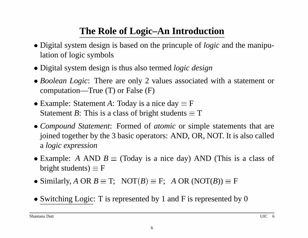
The Role of Logic–An Introduction
� Digital system design is based on the princuple of logic and the manipu-lation of logic symbols
� Digital system design is thus also termed logic design
� Boolean Logic: There are only 2 values associated with a statement orcomputation—True (T) or False (F)
� Example: Statement A: Today is a nice day � FStatement B: This is a class of bright students � T
� Compound Statement: Formed of atomic or simple statements that arejoined together by the 3 basic operators: AND, OR, NOT. It is also calleda logic expression
� Example: A AND B � (Today is a nice day) AND (This is a class ofbright students) � F
� Similarly, A OR B � T; NOT
�
B
�
� F; A OR (NOT(B)) � F
� Switching Logic: T is represented by 1 and F is represented by 0
Shantanu Dutt UIC 6
6

Introduction: The Role of Logic (contd.)
� Defn. A logic function f
�
A1 �
A2 �
� � �
�
An �
, where A1 �
� � �
�
An are logic vari-ables that can take 1/0 values, is one which has either 1 or 0 values as itsoutput depending on the input combination of its 1/0 values
� Fact: Any logic function can be represented by a combination of AND,OR, NOT operators on the input variables
� Fact: Any logic function can also be represented by a Truth Table (TT)
� A Truth Table is a tabular representation of a logic function (or operation)where the output value (1/0) is indicated for each input 1/0 combination.Examples for the AND, OR, NOT functions:
� Defn A logic circuit is a circuit that realizes a logic function f
�
A1 �
� � �
�
An �
”electrically”. It does so by electrically representing 1’s and 0’s as voltagelevels, and manipulating them to produce 1 or 0 at the output as requiredby function f .
Shantanu Dutt UIC 7
7
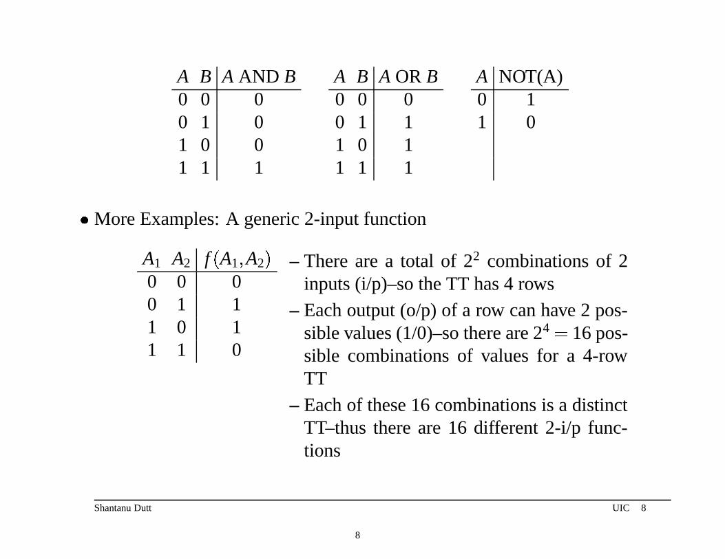
A B A AND B A B A OR B A NOT(A)0 0 0 0 0 0 0 10 1 0 0 1 1 1 01 0 0 1 0 11 1 1 1 1 1
� More Examples: A generic 2-input function
A1 A2 f
�
A1 �
A2 �
0 0 00 1 11 0 11 1 0
– There are a total of 22 combinations of 2inputs (i/p)–so the TT has 4 rows
– Each output (o/p) of a row can have 2 pos-sible values (1/0)–so there are 24 � 16 pos-sible combinations of values for a 4-rowTT
– Each of these 16 combinations is a distinctTT–thus there are 16 different 2-i/p func-tions
Shantanu Dutt UIC 8
8
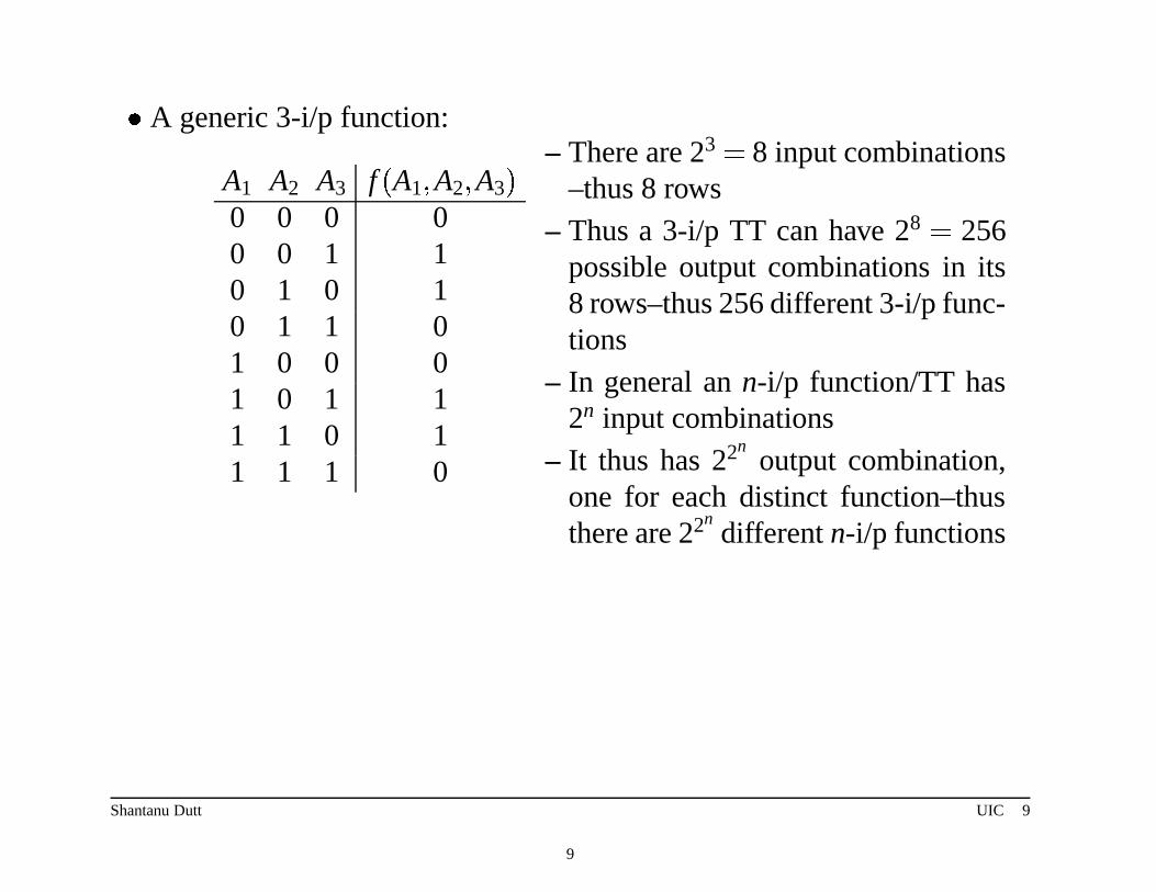
� A generic 3-i/p function:
A1 A2 A3 f
�
A1 �
A2 �
A3 �
0 0 0 00 0 1 10 1 0 10 1 1 01 0 0 01 0 1 11 1 0 11 1 1 0
– There are 23 � 8 input combinations–thus 8 rows
– Thus a 3-i/p TT can have 28 � 256possible output combinations in its8 rows–thus 256 different 3-i/p func-tions
– In general an n-i/p function/TT has2n input combinations
– It thus has 22noutput combination,
one for each distinct function–thusthere are 22n
different n-i/p functions
Shantanu Dutt UIC 9
9

A Simple Design Problem
Problem: Design a logic circuit that allows a light bulb to be controlled bytoggling any one of the two provided switches s1 �
s2.
+5v
+5v
LogicCircuit
S1
S2S2
S1
Bulb
SW
AC Power
Z
10

A Design Problem (Contd.)Design Steps:
1. Encode the input(s) and output(s) of the logic circuit as logic variables sothat C and A are logic expressions
Input Encoding:Switch s1 is pushed � logic input s1 � 1Switch s1 is not pushed � logic input s1 � 0Similarly for switch s2 and logic input variable s2
(In this case we are using the same name for both the input sensor and thecorresponding single input variable–this may not always be the case)Imp. Note: The term s1 � 1 can be more simply represented as thelogic expression s1; the term s1 � 0 can be more simply represented asNOT
�
s1 �
or s̄1
Output Encoding:Turn the (electro-mechanical) switch SW on � logic output Z � 1Turn the (electro-mechanical) switch SW off � logic output Z � 0
Shantanu Dutt UIC 11
11
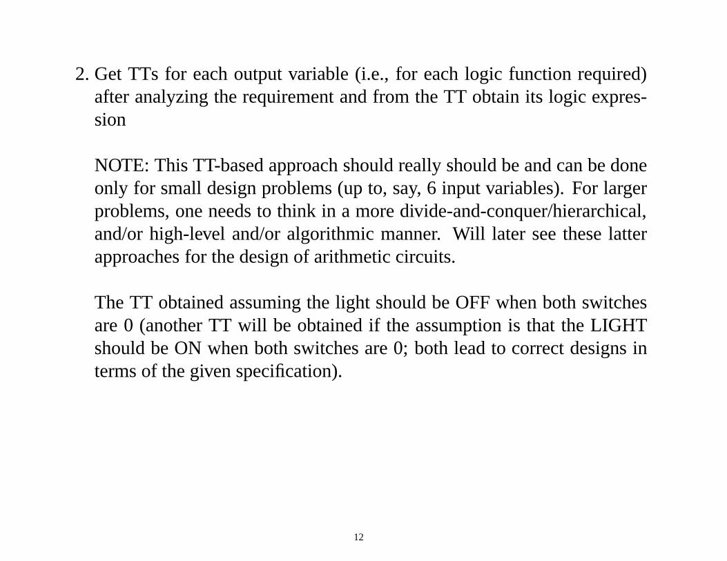
2. Get TTs for each output variable (i.e., for each logic function required)after analyzing the requirement and from the TT obtain its logic expres-sion
NOTE: This TT-based approach should really should be and can be doneonly for small design problems (up to, say, 6 input variables). For largerproblems, one needs to think in a more divide-and-conquer/hierarchical,and/or high-level and/or algorithmic manner. Will later see these latterapproaches for the design of arithmetic circuits.
The TT obtained assuming the light should be OFF when both switchesare 0 (another TT will be obtained if the assumption is that the LIGHTshould be ON when both switches are 0; both lead to correct designs interms of the given specification).
12

s1 s2 Z0 0 00 1 11 0 11 1 0
– Each row in a TT corresponds to an AND term or prod-uct term or minterm of the input variables
– In the product term an i/p variable X occurs as X̄ if itis 0 in that row otherwise as X
– The output column is the OR of all the prod-uct terms (rows) for which it is a 1–thus Z �
�
s̄1 AND s2 �
OR
�
s1 AND s̄2 �
– More compactly, Z �
�
s̄1s2 �
�
�
s1s̄2 �
, product form re-places AND and plus (+) form replaces OR This iscalled a canonical sum-of-product (SOP) expression.
Shantanu Dutt UIC 13
13

3. Minimize the logic expression(s) using various methods like algebraicmanipulation, K-Maps, Quine-McCluskey and Petrick’s algorithm. Theabove expression for Z is already in minimized form.
4. Implement the logic expression(s) using “switches” or “gates” (or some othertechnologies like PLA, multiplexers, ROMs–will do later)
S1
S2
S1S2
NOT gate
AND gate
OR gate
S2S1
S1S2
S2S1 S1S2+Z=
Shantanu Dutt UIC 14
14

Purpose of Hardware Description Language (HDL)
� Q. What is the purpose of describing a digital circuit or system in thismanner?Ans.
– Ease of specifying the design of large circuits/systems using well un-derstood programming language and algorithmic constructs.
Note: Did you know that any algorithm that can be mapped to a pro-gram (in say C++) can also be mapped to hardware that then directlyimplements the algorithm? This is because a program is ultimatelyexecuted by a hardware–a computer, and a direct mapping of the algo-rithm to hardware executes that algorithm by mimicking the computerexecution (as a byproduct of the mapping, for e.g., id there is an ADDoperation to be performed the computer will process it via a generalpurpose ADD instruction while the specialised hardware will processit by sourcing the relevant operands to the inputs of an adder via con-trol signals from a controller).
Shantanu Dutt UIC 16
16

Hardware Synthesis – Example 1
GenerationComputer Code
Unit (FSM)
ldc
lda
ldbCPU
Mux3_select
b c
a
ADDER
Mux
MuxMuxMux2_selectMux1_select
Hardware Synthesis
Exe
cuti
on in
a C
PU
Control
Read Bus A Read Bus B
Mux
Register File
Write Bus
Con
rtol
sig
nals
Conrtol signals
Programming language statement
a := b + c;
Load r5 bLoad r7 c
Store r2 a
(r2 <- r5 + r7)ADD r2 r5 r7
Reg_r/w
Reg_addr
Alu_oper_select
Mux_select
r2
32
ADD ALU
r7
r5
3232
Shantanu Dutt UIC 17
17
Hardware Synthesis – Example 2
O/Ps of code block
I/Ps to code block
SynthesizedRecursively
Computer
a computerExecution in
10
10
ldblda
Mux1_select
zero
ovflsign
Demux1_selectDemux
Block B forHardware
Mux
2’s compl
ba
Hardware Synthesis
Block B Adder
Block A forHardware
GenerationComputer Code
Programming language construct
end Block B of code;else beginend Block A of code;if (a <= b) then begin
assmb code
operations)
(Adder may bereused for other
Unit (FSM)Control
Con
rtol
sig
nals
Conrtol signals
Block C
B:
Load r3 bLoad r2 a
BZ ABNEG A
SUB r2 r2 r3
assmb codeBlock AA:JMP C
assmb codeC:
Shantanu Dutt UIC 18
18

Purpose of HDL (contd.)– Simulating and testing designs for correctness before actual implemen-
tation/fabrication.– Automatic synthesis of large designs specified behaviorally or algo-
rithmically using CAD tools:
� can also verify each transformation (algorithm � circuit (netlist) �
chip layout) using verification tools
� reduces human error
� increases design productivity
� can lead to more innovative designs as it frees the designer fromwell-known nitty-gritty details of circuit design (e.g., design oifa fast adder) allowing the designer to explore alternative de-signs/algorithms at a higher level
Shantanu Dutt UIC 19
19
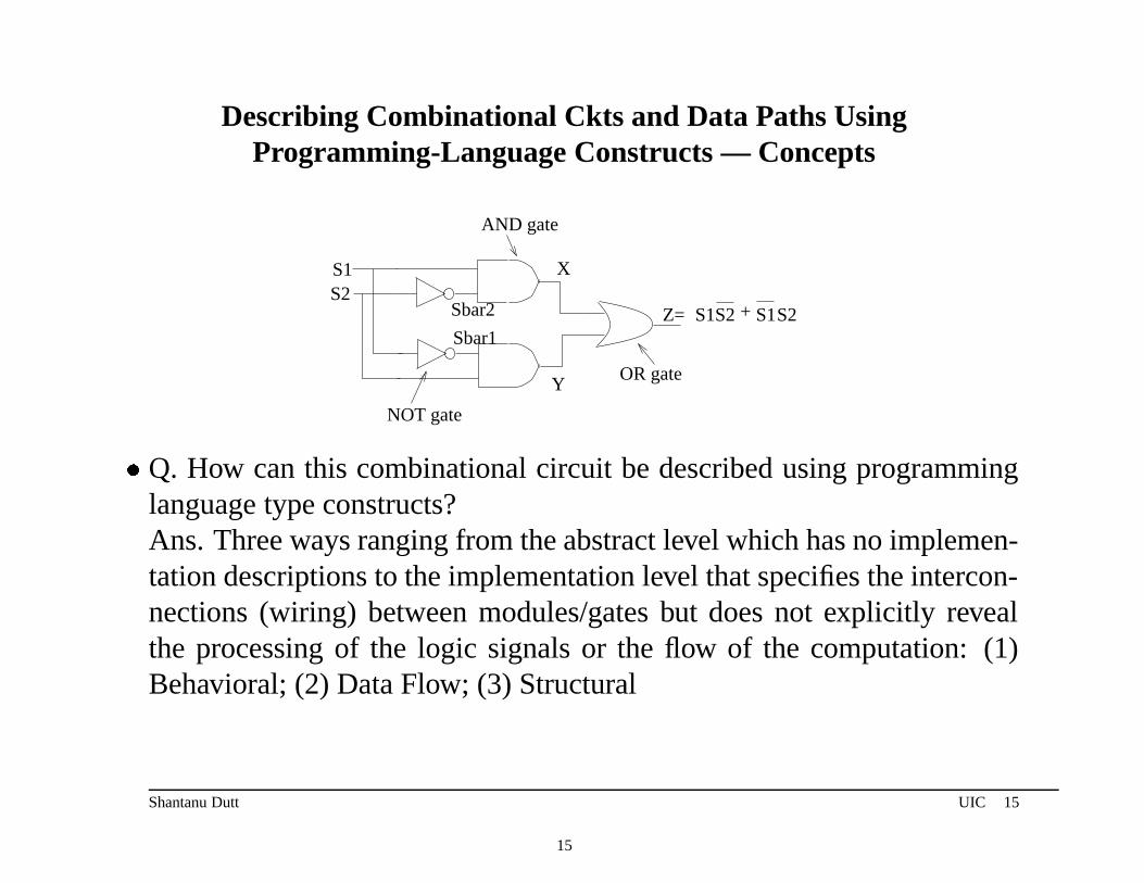
Describing Combinational Ckts and Data Paths UsingProgramming-Language Constructs — Concepts
S1S2
NOT gate
AND gate
OR gate
X
Y
Sbar2
Sbar1S2S1 S1S2+Z=
� Q. How can this combinational circuit be described using programminglanguage type constructs?Ans. Three ways ranging from the abstract level which has no implemen-tation descriptions to the implementation level that specifies the intercon-nections (wiring) between modules/gates but does not explicitly revealthe processing of the logic signals or the flow of the computation: (1)Behavioral; (2) Data Flow; (3) Structural
Shantanu Dutt UIC 15
15
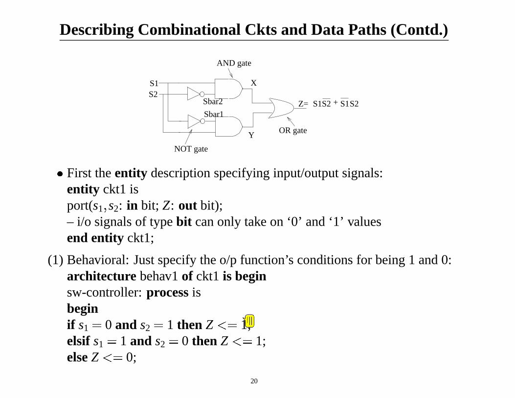
Describing Combinational Ckts and Data Paths (Contd.)
S1S2
NOT gate
AND gate
OR gate
X
Y
Sbar2
Sbar1S2S1 S1S2+Z=
� First the entity description specifying input/output signals:entity ckt1 isport(s1 �
s2: in bit; Z: out bit);– i/o signals of type bit can only take on ‘0’ and ‘1’ valuesend entity ckt1;
(1) Behavioral: Just specify the o/p function’s conditions for being 1 and 0:architecture behav1 of ckt1 is beginsw-controller: process isbeginif s1 � 0 and s2 � 1 then Z � � 1;elsif s1 � 1 and s2 � 0 then Z � � 1;else Z � � 0;
20
end if;end process sw-controller;end architecture behav1;
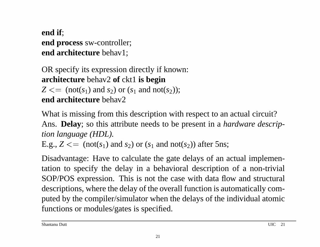
OR specify its expression directly if known:architecture behav2 of ckt1 is beginZ � � (not(s1) and s2) or (s1 and not(s2));end architecture behav2
What is missing from this description with respect to an actual circuit?Ans. Delay; so this attribute needs to be present in a hardware descrip-tion language (HDL).E.g., Z � � (not(s1) and s2) or (s1 and not(s2)) after 5ns;
Disadvantage: Have to calculate the gate delays of an actual implemen-tation to specify the delay in a behavioral description of a non-trivialSOP/POS expression. This is not the case with data flow and structuraldescriptions, where the delay of the overall function is automatically com-puted by the compiler/simulator when the delays of the individual atomicfunctions or modules/gates is specified.
Shantanu Dutt UIC 21
21
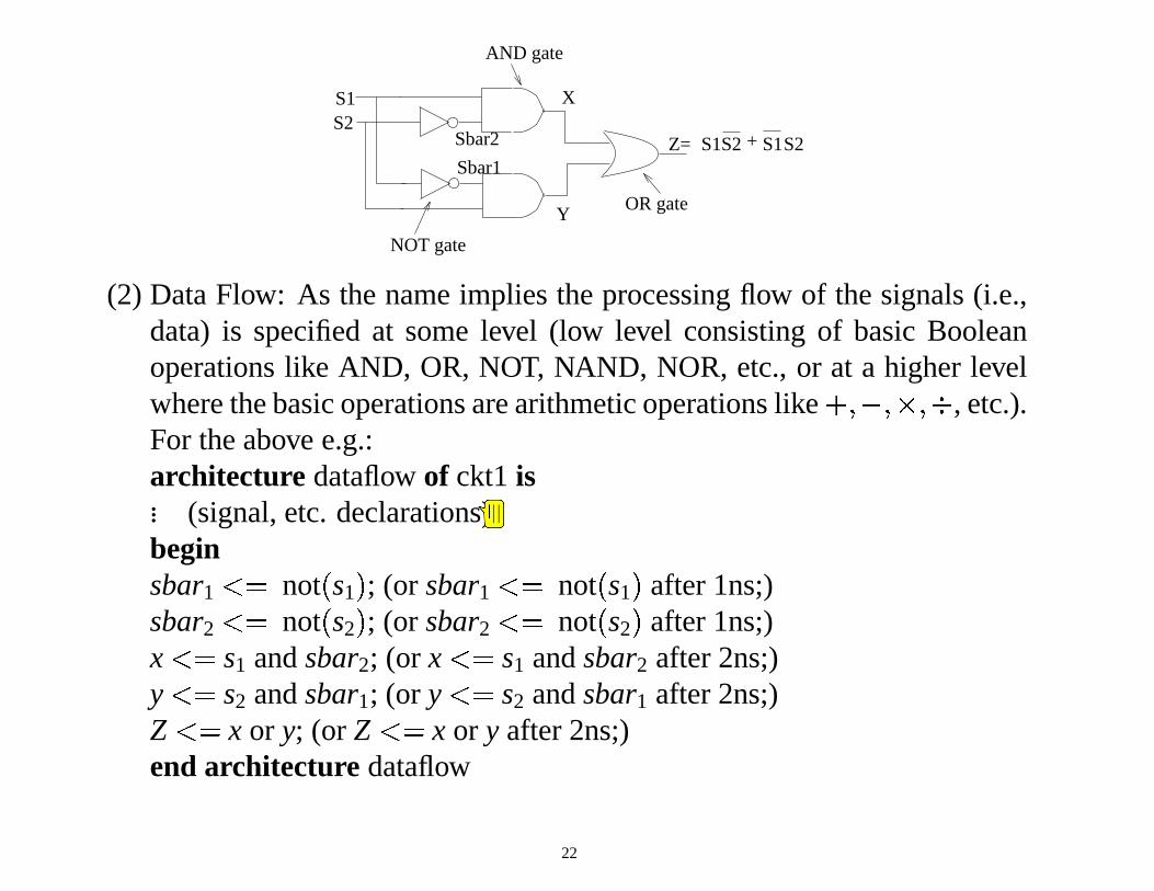
S1S2
NOT gate
AND gate
OR gate
X
Y
Sbar2
Sbar1S2S1 S1S2+Z=
(2) Data Flow: As the name implies the processing flow of the signals (i.e.,data) is specified at some level (low level consisting of basic Booleanoperations like AND, OR, NOT, NAND, NOR, etc., or at a higher levelwhere the basic operations are arithmetic operations like �
��
��
�� , etc.).
For the above e.g.:architecture dataflow of ckt1 is... (signal, etc. declarations)beginsbar1 � � not
�
s1 �
; (or sbar1 � � not�
s1 �
after 1ns;)sbar2 � � not
�
s2 �
; (or sbar2 � � not
�
s2 �
after 1ns;)x � � s1 and sbar2; (or x � � s1 and sbar2 after 2ns;)y � � s2 and sbar1; (or y � � s2 and sbar1 after 2ns;)Z � � x or y; (or Z � � x or y after 2ns;)end architecture dataflow
22
where sbar1 �
sbar2 �
x
�
y are intermediate signals. Notice how the process-ing of the function Z is described in detail via all intermediate signals.
– The above statements are called concurrent statements are to be ex-ecuted concurrently (i.e., simulated concurrency) by a simulator andnot sequentially as in a regular programming language.
– Concurrent statements represent hardware perfectly since the hardwareis always “executing” each statement concurrently!
– A statement is executed only when one of the signals, say, x on itsleft hand side (LHS) changes—this is called an event on x and such asimulation of a circuit is called a discrete event simulation.
– There are also sequential statements in VHDL which are included in aprocess definition as in the behavioral description of the circuit givenearlier.
– Statements in a process are executed in order of their appearance se-quentially just like statements in a regular programming language.
Shantanu Dutt UIC 23
23

– For initialization, each signal is just initialized to its "leftmost"
value (e.g., for "bit" type this is '0').
round i+1

Discrete Event Simulation – E.g. w/o Delays
sbar1 � � not
�
s1 �
; sbar2 � � not
�
s2 �
;x � � s1 and sbar2; y � � s2 and sbar1;Z � � x or y;
� Start: s1 � 0
�
s2 � 0
�
sbar1 � 1
�
sbar2 � 1
�
x � 0
�
y � 0
�
Z � 0
� Rnd 1 (I/P signal s2 changes): s1 � 0
�
s2 � 1
�
sbar1 � 1�
sbar2 � 1
�
x �
0
�
y � 0
�
Z � 0Eval sbar2 � � not
�
s2 �
; The value ‘0’ is scheduled on sbar2.Eval y � � s2 and sbar1; The value ‘1’ is scheduled on y.
� Rnd 2: s1 � 0
�
s2 � 1
�
sbar1 � 1
�
sbar2 � 0�
x � 0
�
y � 1
�
Z � 0Eval x � � s1 and sbar2; No change in x, so no event scheduled on xEval Z � � x or y; The value ‘1’ is scheduled on Z.
� Rnd 3: s1 � 0
�
s2 � 1
�
sbar1 � 1�
sbar2 � 0
�
x � 0
�
y � 1
�
Z � 1No new events are scheduled.Simulation suspends until the value of some signal (generally, input)changes.
Shantanu Dutt UIC 26
26
Discrete Event Simulation – With Delays
– The first three definitions and issues (about event, when simulation isperformed of statements and modules, and the initial evaluations) alsoapply in DES with delays. In addition we have the following concepts.
– The current simulation time is the circuit time till which the DES hasperformed simulations of the various statements or modules of the circuit.
– If a delay of, say, 10 ns, is associated with an output signal X and whenits coresponding statement is executed its value changes, then X is putin the event queue with a time tag of
�
t � 10
�
ns, where t is the currentsimulation time.
– The event queue is kept sorted by increasing time tags and the DES pickssignals to be displayed from the beginning of the event queue.
– Statement/module evaluation takes place at acertain time t after all sig-nals scheduled for display at time t are displayed and their new values as-serted. Only those statements/modules are evaluated which have at leastone input from these displayed signals.
– The current simulation time is the time tag of the statement or modulepicked from the event queue to be executed.
– Instead of rounds, we now have the concept of simulation time.
27

Discrete Event Simulation — Event Queue for Simulation w/ Delays
Statements: �� �� � �� � � � � �� � �� �� � � � � � � � � �� � � � � �� � �� �� � � �
� �� � �� � � � � � � � � � �� �� � � � � �� � � � � � � � �� �� � �� �� � � �
� �� �� � � � � �� �� � � �
T=t
sbar1 =0
T=t+1
x=1
T=t+2
x=1
T=t+2
At time t+2: disp x=1 & execute Z <= x or y after 2ns;Result −> 1 event: Z: 0 −> 1 @ t+4 ns;
At time t+4: disp Z=1, no statement execution
Z=1
T=t+4
S1=1
Available @ time
At time t: S1: 0−>1, S2=0, Sbar1=1, Sbar2=1, x=0, y=0, Z=0
Event Q
Result −> 2 events: sbar1: 1−>0 @ t+1 ns, x: 0−>1 @ t+2 ns
At time t: display S1 = 1 &execute sbar1 <= not(s1) after 1ns; x <= s1 and sbar2 after 2ns;
At time t+1: disp sbar1=0 & execute y <= s2 and sbar1 after 2ns;Result −> 0 events: y: 0 −> 0;
New valueEvent
(a)
(b)
DES with delays
c� Shantanu Dutt, UIC 28

Discrete Event Simulation – E.g. With Delays
sbar1 � � not
�
s1 �
after 1ns; sbar2 � � not
�
s2 �
after 1ns;x � � s1 and sbar2 after 2ns; y � � s2 and sbar1 after 2ns;Z � � x or y after 2ns;
S1
S2
Sbar1
Sbar2
x
y
Z
1ns 2ns 3ns 4ns 5ns 6ns
Eval Sbar2 <= not(S2) @ t =1ns
Eval x <= S1 and Sbar2 @ t=2ns (no change in x)
Eval y <= S2 and Sbar1 @ t=1ns
Eval Z <= x or y @ t=3ns
event
event
event
Shantanu Dutt UIC 29
29

Discrete Event Simulation — Event Queue for Simulation w/o Delays
� Statements: �� �� � �� � � � � � �� �� � �� � � � � �
� � � � �� � � �� � � � � �� � � � � � �� �� � � � � �� � �
� In actuality, statements with delays are simulated in a similar way as statements with delays by assigninga “fictitious” � delay to a statement w/o delays.
� So a statement � � � � �� � � �� �� � ; becomes equivalent to � �� � �� � � �� �� � � � �� � � ;
� The following rules apply to such statements: (a) � � � � � if � � � . (b) � � � any specified “real” delayhowever small (e.g., 1 fs).
� These rules and the concept of fictitious � delays allows treatment of statements with and without delayspecifications to be treated in an uniform manner, as illustrated below:
~ Round 1
S1=1T=t
Z=1
T=t+2del
At time t+2del: disp Z=1, no statement execution
~ Round 2
Available @ time
At time t: S1: 0−>1, S2=0, Sbar1=1, Sbar2=1, x=0, y=0, Z=0
Event Q
Result −> 2 events: sbar1: 1−>0 @ t+ del, x: 0−>1 @ t+del.
At time t: display S1 = 1 &execute sbar1 <= not(s1); x <= s1 and sbar2;
At time t+del: disp sbar1=0, x=1, &
sbar1 =0
T=t+del
x=1
T=t+del
execute: y<= s2 and sbar1; Z <= x or y after 2ns;Result −> 1 event: Z: 0 −> 1 @ t+ 2*del;
Event New value
DES without delays
c� Shantanu Dutt, UIC 30

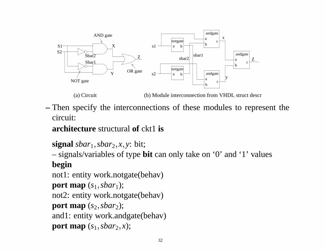
Back to Description of Combinational Ckts and Data Paths
(3) Structural:
– Specify the interconnection of the modules/gates. The modules/gatesthemselves need to be described as separate entities in either a behav-ioral, data-flow or structural manner and so forth.
– A structural (or mixed) description also allows us to specify the designin a top-down hierarchical manner.
– However, the algorithm, data flow, etc. of the processing is not clearlyevident in such a description.
– Such a description is mainly used for simulation and testing to verifythe correctness of a circuit level design.
For the above e.g.:
S1S2
NOT gate
AND gate
OR gate
X
Y
Sbar2
Sbar1S2S1 S1S2+Z=
– First declare the input/output ports or signals of each module (enclosed
30

architecture behav of orgate is
begin
c <= a or b after 2 ns;
-- “or” is an inbuild operator of VHDL
end architecture behav;
(a) Circuit (b) Module interconnection from VHDL struct descr
ZSbar2
Sbar1
Y
X
OR gate
AND gate
NOT gate
S2S1
ac
b
andgate
ac
b
andgate
banotgate
banotgate
sbar1sbar2
s2
s1
y
x
Zac
b
andgate
– Then specify the interconnections of these modules to represent thecircuit:architecture structural of ckt1 is
signal sbar1 �
sbar2 �
x
�
y: bit;– signals/variables of type bit can only take on ‘0’ and ‘1’ valuesbeginnot1: entity work.notgate(behav)port map (s1 �
sbar1);not2: entity work.notgate(behav)port map (s2 �
sbar2);and1: entity work.andgate(behav)port map (s1 �
sbar2 �
x);
32

and2: entity work.andgate(behav)port map (s2 �
sbar1 �
y);or1: entity work.orgate(behav)port map (x
�
y
�
z);end architecture structural;
� The above type of component instantiation is available only in VHDL-90and is called direct instantiation. This will not work in VHDL-87. Willshow instantiation mechanism later for VHDL-87.
� Note that multiple architecture definitions are possible in VHDL for thesame circuit/system.
Shantanu Dutt UIC 33
33

Alternate Structural Description Library IEEE; use IEEE.STD_LOGIC_1164.all; entity ckt1 is port(s1,s2:in bit; Z:out bit); end entity ckt1; architecture structure of ckt1 is component and_gate is port(x,y:in bit; z:out bit); end component and_gate; component not_gate is port(x:in bit; y:out bit); end component not_gate; component or_gate is port(x,y:in bit; z:out bit); end component or_gate; signal sbar1,sbar2,X,Y:bit; begin N1:not_gate port map(s1,sbar1); N2:not_gate port map(s2,sbar2); and1:and_gate port map(s1,sbar2,X); and2:and_gate port map(s2,sbar1,Y); or1:or_gate port map(X,Y,Z); end architecture structure;
Summary
Discussed the following:
� Uses of HDL
� Entity (generic parameters, i/o signals), architecture (functional and/ormechanism descriptions) and binding (which entity-architecture combi-nations to use for the instantiated components (if any)—confi guration de-scription, direct instantiation, etc.) descriptions of a VHDL module
� Three types of architecture descriptions: behavioral, dataflow, structural.Behavioral descriptions can be done at many levels. A mixed descriptionincorporates elements of 2 or more of the above types
� Concurrent statements, sequential statements & processes—basic con-cepts
� Discrete event simulation of statements w/ and w/o delays
– Concepts of events, event Q, simulation time
– Concept of � -delays to tackle statements w/o delays
c� Shantanu Dutt, UIC 34