ec7451: microprocessor and microcontroller iv- microcontroller_final_4march2020.pdf8051...
TRANSCRIPT
EC7451: MICROPROCESSOR AND MICROCONTROLLER
Dr. V. SATHIESH KUMAR Department of Electronics Engg., MIT1
Presentation Slides:
www.sathieshkumar.com/tutorials
Unit IV : MICROCONTROLLER1. 8051 – Architecture and pindetails2. Special Function Registers (SFRs)3. I/O Ports, Timers / counters4. Interrupts and serial communication5. Instruction set 6. Addressing modes7. Assembly language programming TEXT BOOKMuhammad Ali Mazidi, Janice Gillispie Mazidi and Rolin D. McKinley, "The 8051Microcontroller and Embedded Systems", Second Edition, Pearson Education 2008. Fifthimpression 2011
Presented By,
Dr. V. Sathiesh Kumar Department of Electronics Engg.,
MIT-Anna University
EC7451: MICROPROCESSOR AND MICROCONTROLLER UNIT IV – Microcontroller
Dr. V. SATHIESH KUMAR Department of Electronics Engg., MIT2
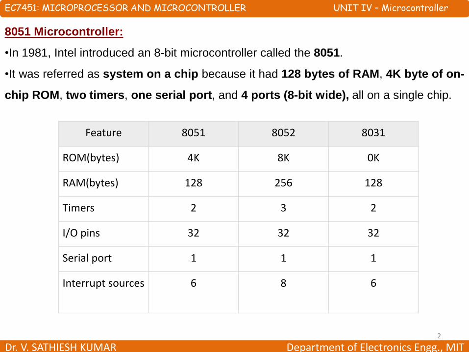
8051 Microcontroller:
•In 1981, Intel introduced an 8-bit microcontroller called the 8051.
•It was referred as system on a chip because it had 128 bytes of RAM, 4K byte of on-
chip ROM, two timers, one serial port, and 4 ports (8-bit wide), all on a single chip.
Feature 8051 8052 8031
ROM(bytes) 4K 8K 0K
RAM(bytes) 128 256 128
Timers 2 3 2
I/O pins 32 32 32
Serial port 1 1 1
Interrupt sources 6 8 6
EC7451: MICROPROCESSOR AND MICROCONTROLLER UNIT IV – Microcontroller
Dr. V. SATHIESH KUMAR Department of Electronics Engg., MIT3
8051 Microcontroller: Features
•An 8051 microcontroller comes with the following features −
1. 4KB bytes on-chip program memory (ROM)
2. 128 bytes on-chip data memory (RAM)
3. Four register banks
4. 8-bit bidirectional data bus
5. 16-bit unidirectional address bus
6. 32 general purpose registers, each of 8-bit
7. 16 bit Timers (usually 2, but may have more or less)
8. Three internal and two external Interrupts
9. Four 8-bit ports
10.16-bit program counter and data pointer
EC7451: MICROPROCESSOR AND MICROCONTROLLER UNIT IV – Microcontroller
Dr. V. SATHIESH KUMAR Department of Electronics Engg., MIT4
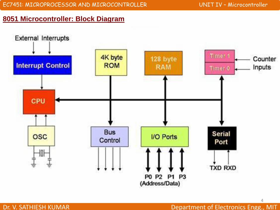
8051 Microcontroller: Block Diagram
EC7451: MICROPROCESSOR AND MICROCONTROLLER UNIT IV – Microcontroller
Dr. V. SATHIESH KUMAR Department of Electronics Engg., MIT5
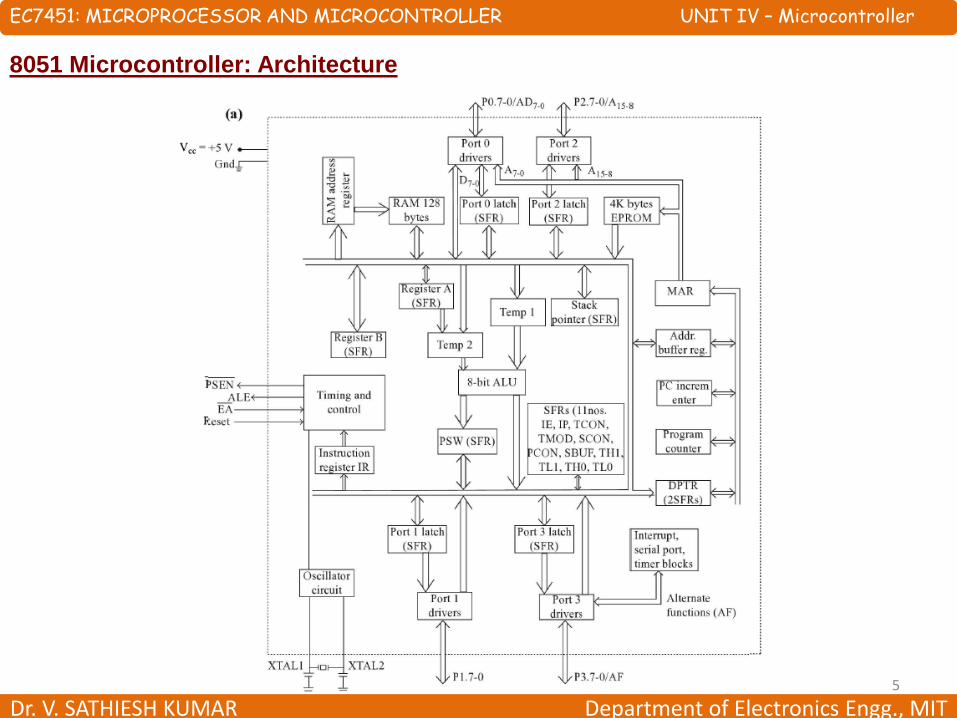
8051 Microcontroller: Architecture
EC7451: MICROPROCESSOR AND MICROCONTROLLER UNIT IV – Microcontroller
Dr. V. SATHIESH KUMAR Department of Electronics Engg., MIT6
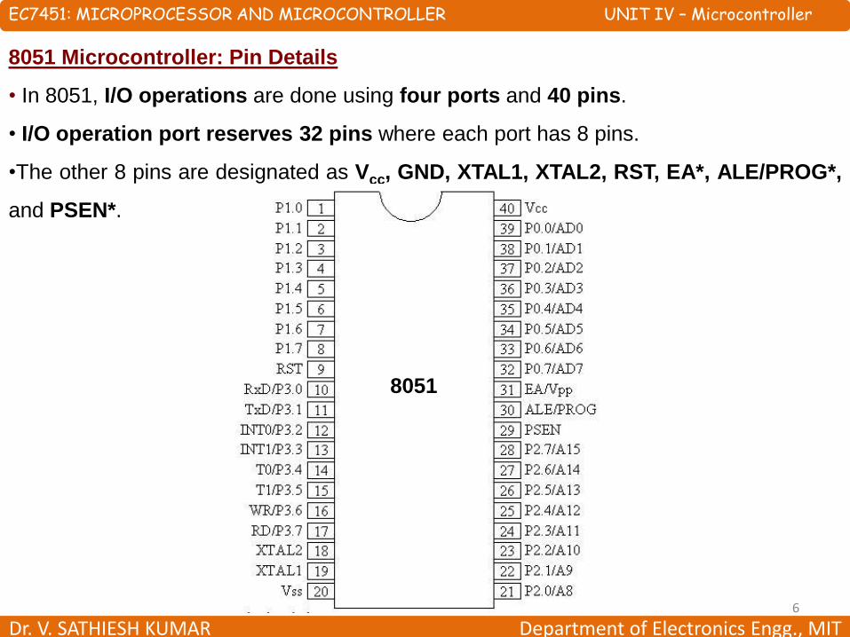
8051 Microcontroller: Pin Details
• In 8051, I/O operations are done using four ports and 40 pins.
• I/O operation port reserves 32 pins where each port has 8 pins.
•The other 8 pins are designated as Vcc, GND, XTAL1, XTAL2, RST, EA*, ALE/PROG*,
and PSEN*.
8051
EC7451: MICROPROCESSOR AND MICROCONTROLLER UNIT IV – Microcontroller
Dr. V. SATHIESH KUMAR Department of Electronics Engg., MIT7
8051 Microcontroller: Pin Details - I/O Port and their functions
• The four ports P0, P1, P2, and P3, each use 8 pins, making them 8-bit ports.
•Upon RESET, all the ports are configured as inputs, ready to be used as input ports.
• When the first 0 is written to a port, it becomes an output.
•To reconfigure it as an input, a 1 must be sent to a port.
Port 0 (Pin No 32 – Pin No 39):
•It has 8 pins (32 to 39).
•It can be used for input or output.
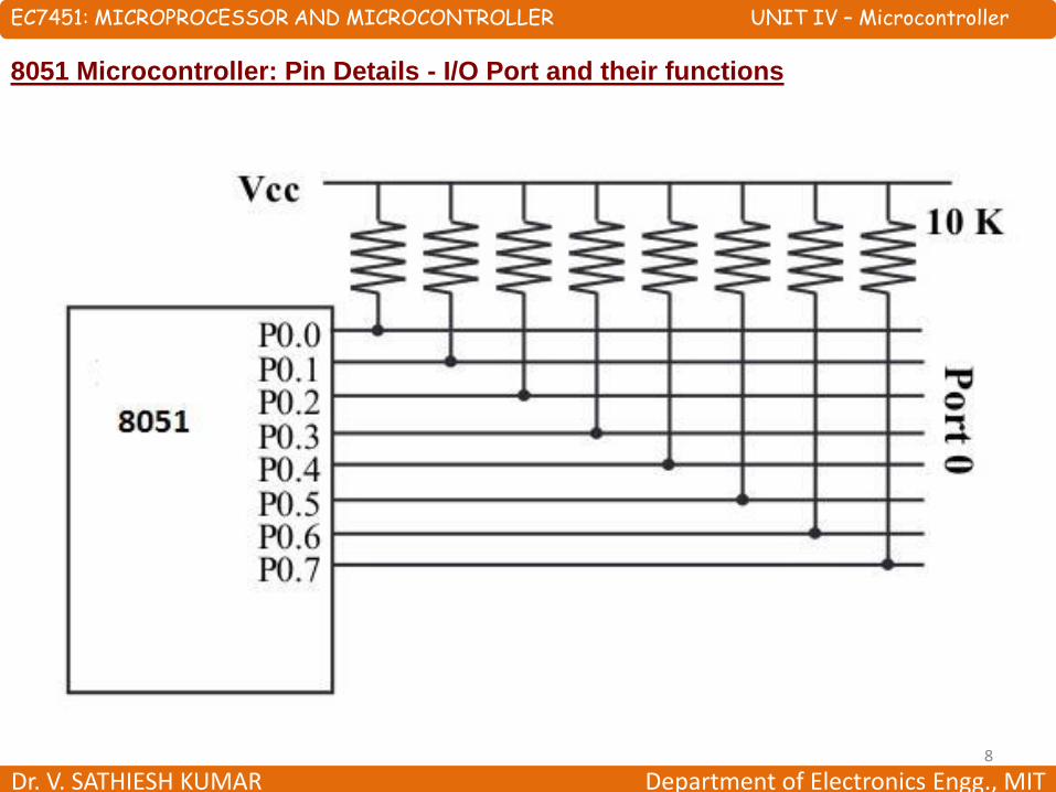
•Unlike P1, P2, and P3 ports, we normally connect P0 to 10K-ohm pull-up resistors
to use it as an input or output port being an open drain.
•It is also designated as AD0-AD7, allowing it to be used as both address and data.
•ALE (Pin no 31) indicates if P0 has address or data.
•When ALE = 0, it provides data D0-D7, but when ALE = 1, it has address A0-A7.
EC7451: MICROPROCESSOR AND MICROCONTROLLER UNIT IV – Microcontroller
Dr. V. SATHIESH KUMAR Department of Electronics Engg., MIT8
8051 Microcontroller: Pin Details - I/O Port and their functions

EC7451: MICROPROCESSOR AND MICROCONTROLLER UNIT IV – Microcontroller
Dr. V. SATHIESH KUMAR Department of Electronics Engg., MIT9
8051 Microcontroller: Pin Details - I/O Port and their functions
Port 1 (Pin No 1 – Pin No 8):
•It is an 8-bit port (pin 1 through 8) and can be used either as input or output.
•It doesn't require pull-up resistors because they are already connected internally.
•Upon RESET, Port 1 is configured as an input port.
•If Port 1 is configured to be used as an output port, then to use it as an input port again,
program it by writing 1 to all of its bits.
Port 2 (Pins 21 through 28):
•Port 2 occupies a total of 8 pins (pins 21 through 28) and can be used for both input
and output operations.
• P2 also doesn't require external Pull-up resistors because they are already
connected internally.
•It must be used along with P0 to provide the 16-bit address for the external
memory.
EC7451: MICROPROCESSOR AND MICROCONTROLLER UNIT IV – Microcontroller
Dr. V. SATHIESH KUMAR Department of Electronics Engg., MIT10
8051 Microcontroller: Pin Details - I/O Port and their functions
•When the 8051 is connected to an external memory, it provides path for upper 8-
bits of 16-bits address, and it cannot be used as I/O.
•Upon RESET, Port 2 is configured as an input port.
•If Port 2 is configured to be used as an output port, then to use it as an input port again,
program it by writing 1 to all of its bits.
Port 3 (Pins 10 through 17):
• It is also of 8 bits and can be used as Input/Output.
•P3.0 and P3.1 are RxD (Receiver) and TxD (Transmitter), respectively and are
collectively used for Serial Communication.
•P3.2 and P3.3 pins are used for external interrupts.
•P3.4 and P3.5 are used for timers T0 and T1, respectively.
•P3.6 and P3.7 are Write (WR*) and Read (RD*) pins.
EC7451: MICROPROCESSOR AND MICROCONTROLLER UNIT IV – Microcontroller
Dr. V. SATHIESH KUMAR Department of Electronics Engg., MIT11
8051 Microcontroller: Pin Details - I/O Port and their functions
•Vcc − Pin 40 provides supply to the Chip and it is +5 V.
•Gnd − Pin 20 provides ground for the Reference.
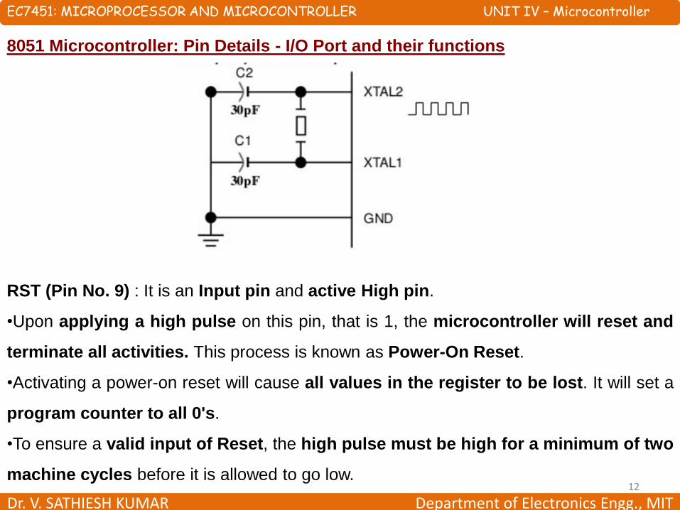
XTAL1, XTAL2 (Pin no 18 & Pin no 19): 8051 has on-chip oscillator but requires
external clock to run it.
• A quartz crystal is connected between the XTAL1 and XTAL2 pin of the chip.
•This crystal also needs two capacitors of 30pF for generating a signal of desired
frequency.
•One side of each capacitor is connected to ground.
•8051 IC is available in various speeds and it all depends on this Quartz crystal.
•For example, a 20 MHz microcontroller requires a crystal with a frequency no more
than 20 MHz.
EC7451: MICROPROCESSOR AND MICROCONTROLLER UNIT IV – Microcontroller
Dr. V. SATHIESH KUMAR Department of Electronics Engg., MIT12
8051 Microcontroller: Pin Details - I/O Port and their functions
RST (Pin No. 9) : It is an Input pin and active High pin.
•Upon applying a high pulse on this pin, that is 1, the microcontroller will reset and
terminate all activities. This process is known as Power-On Reset.
•Activating a power-on reset will cause all values in the register to be lost. It will set a
program counter to all 0's.
•To ensure a valid input of Reset, the high pulse must be high for a minimum of two
machine cycles before it is allowed to go low.
EC7451: MICROPROCESSOR AND MICROCONTROLLER UNIT IV – Microcontroller
Dr. V. SATHIESH KUMAR Department of Electronics Engg., MIT13
8051 Microcontroller: Pin Details - I/O Port and their functions
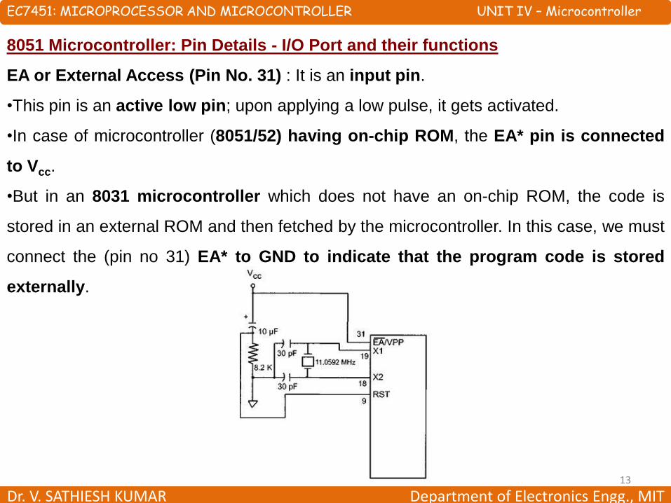
EA or External Access (Pin No. 31) : It is an input pin.
•This pin is an active low pin; upon applying a low pulse, it gets activated.
•In case of microcontroller (8051/52) having on-chip ROM, the EA* pin is connected
to Vcc.
•But in an 8031 microcontroller which does not have an on-chip ROM, the code is
stored in an external ROM and then fetched by the microcontroller. In this case, we must
connect the (pin no 31) EA* to GND to indicate that the program code is stored
externally.

EC7451: MICROPROCESSOR AND MICROCONTROLLER UNIT IV – Microcontroller
Dr. V. SATHIESH KUMAR Department of Electronics Engg., MIT14
8051 Microcontroller: Pin Details - I/O Port and their functions
PSEN* or Program store Enable (Pin No 29) : This is also an active low pin, i.e., it
gets activated after applying a low pulse.
•It is an output pin and used along with the EA* pin in 8031 based (i.e. ROMLESS)
Systems to allow storage of program code in external ROM.
ALE or (Address Latch Enable) : This is an Output Pin and is active high.
•It is especially used for 8031 IC to connect it to the external memory.
•It can be used while deciding whether P0 pins will be used as Address bus or Data
bus.
•When ALE = 1, then the P0 pins work as Address bus and when ALE = 0, then the
P0 pins act as Data bus.

EC7451: MICROPROCESSOR AND MICROCONTROLLER UNIT IV – Microcontroller
Dr. V. SATHIESH KUMAR Department of Electronics Engg., MIT15
8051 Microcontroller: Little Endian vs Big Endian
•Although numbers are always displayed in the same way, they are not stored in
the same way in memory.
•Big-Endian machines store the most significant byte of data in the lowest memory
address.
•A Big-Endian machine stores 0x12345678 as −
ADD+0: 0x12
ADD+1: 0x34
ADD+2: 0x56
ADD+3: 0x78
EC7451: MICROPROCESSOR AND MICROCONTROLLER UNIT IV – Microcontroller
Dr. V. SATHIESH KUMAR Department of Electronics Engg., MIT16
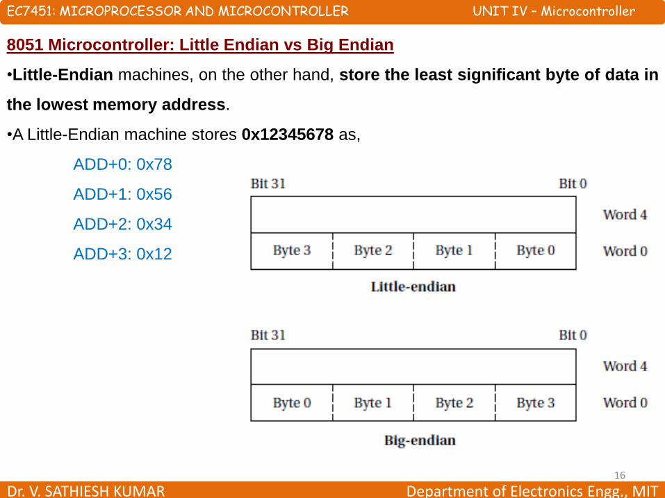
8051 Microcontroller: Little Endian vs Big Endian
•Little-Endian machines, on the other hand, store the least significant byte of data in
the lowest memory address.
•A Little-Endian machine stores 0x12345678 as,
ADD+0: 0x78
ADD+1: 0x56
ADD+2: 0x34
ADD+3: 0x12
EC7451: MICROPROCESSOR AND MICROCONTROLLER UNIT IV – Microcontroller
Dr. V. SATHIESH KUMAR Department of Electronics Engg., MIT17
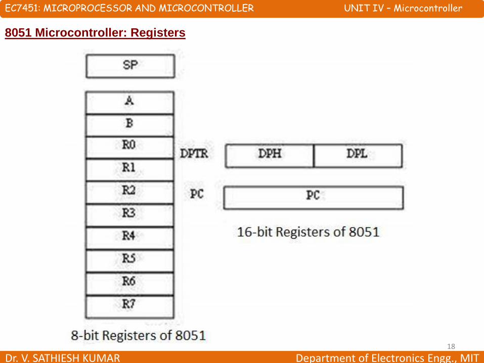
8051 Microcontroller: Registers
•Registers are used in the CPU to store information on temporarily basis which
could be a data to be processed, or an address pointing to the data.
•In 8051, there is one data type is of 8-bits, from the MSB (most significant bit) D7 to
the LSB (least significant bit) D0.
•With 8-bit data type, any data type larger than 8-bits must be broken into 8-bit
chunks before it is processed.
•The most widely used registers of the 8051 are,
1. Accumulator (A) – 8 bits
2. R register (R0 to R7) - 8 bits
3. B register - 8 bits
4. Data Pointer (DPTR) - 16 bits
5. Program Counter (PC) - 16 bits
6. Stack Pointer (SP) - 8 bits
•All these registers are of 8-bits, except DPTR and PC are 16-bit registers.
EC7451: MICROPROCESSOR AND MICROCONTROLLER UNIT IV – Microcontroller
Dr. V. SATHIESH KUMAR Department of Electronics Engg., MIT18
8051 Microcontroller: Registers
EC7451: MICROPROCESSOR AND MICROCONTROLLER UNIT IV – Microcontroller
Dr. V. SATHIESH KUMAR Department of Electronics Engg., MIT19
8051 Microcontroller: Registers
Accumulator (A):
•The accumulator, register A, is used for all arithmetic and logic operations.
•If the accumulator is not present, then every result of each calculation (addition,
multiplication, shift, etc.) is to be stored into the main memory.
•Access to main memory is slower than access to a register like the accumulator
because the technology used for the large main memory is slower (but cheaper)
than that used for a register.
The ‘R’ Registers:
•The „R‟ registers are a set of eight registers, namely, R0, R1 to R7.
•These registers function as auxiliary or temporary storage registers in many
operations.
EC7451: MICROPROCESSOR AND MICROCONTROLLER UNIT IV – Microcontroller
Dr. V. SATHIESH KUMAR Department of Electronics Engg., MIT20
8051 Microcontroller: Registers
The ‘B’ Register:
•The „B‟ register is very similar to the Accumulator in the sense that it may hold an 8-
bit (1-byte) value.
•The "B" register is used only by two 8051 instructions: MUL AB and DIV AB.
•To quickly and easily multiply or divide A by another number, you may store the other
number in „B‟ and make use of these two instructions.
•Apart from using MUL and DIV instructions, the "B" register is often used as yet
another temporary storage register, much like a ninth R register.
The Data Pointer:
•The Data Pointer (DPTR) is the 8051‟s only user-accessible 16-bit (2-byte) register.
•DPTR is meant for pointing to data in external memory.
EC7451: MICROPROCESSOR AND MICROCONTROLLER UNIT IV – Microcontroller
Dr. V. SATHIESH KUMAR Department of Electronics Engg., MIT21
8051 Microcontroller: Registers
The Program Counter:
•The Program Counter (PC) is a 2-byte address (16-bit register) which tells the 8051
where the next instruction to execute can be found in the memory.
•PC starts at 0000H when the 8051 initializes and is incremented every time after an
instruction is executed.
•PC is not always incremented by 1.
•Some instructions may require 2 or 3 bytes; in such cases, the PC will be
incremented by 2 or 3.
•Branch, jump, and interrupt operations load the Program Counter with an
address other than the next sequential location.
•Activating a power-on reset will cause all values in the register to be lost. It means
the value of the PC is 0 upon reset, forcing the CPU to fetch the first opcode from the
ROM location 0000H.
EC7451: MICROPROCESSOR AND MICROCONTROLLER UNIT IV – Microcontroller
Dr. V. SATHIESH KUMAR Department of Electronics Engg., MIT22
8051 Microcontroller: Registers
The Stack Pointer (SP):
•Stack is implemented in RAM and a CPU register is used to access it called SP
(Stack Pointer) register.
•Stack is a upward growing stack (Memory address increase with every insertion
of data into stack).
•SP register is an 8-bit register and can address memory addresses of range 00H to
FFH.
•The Stack Pointer tells the location from where the next value is to be removed
from the stack.
•When the content of a CPU register is stored in a stack, it is called a PUSH
operation.
•When a value is pushed onto the stack, the value of SP is incremented and then
the value is stored at the resulting memory location.
EC7451: MICROPROCESSOR AND MICROCONTROLLER UNIT IV – Microcontroller
Dr. V. SATHIESH KUMAR Department of Electronics Engg., MIT23
8051 Microcontroller: Registers
•When the content of a stack is stored in a CPU register, it is called a POP operation.
•When a value is popped off the stack, the value is returned from the memory
location indicated by SP, and then the value of SP is decremented.
•SP will be initialized to 07H when the 8051 is initialized.
•If a value is pushed onto the stack at the same time, the value will be stored in the
internal RAM address 08H.
•SP is modified directly by the 8051 by six instructions: PUSH, POP, ACALL, LCALL,
RET, and RETI.
EC7451: MICROPROCESSOR AND MICROCONTROLLER UNIT IV – Microcontroller
Dr. V. SATHIESH KUMAR Department of Electronics Engg., MIT24
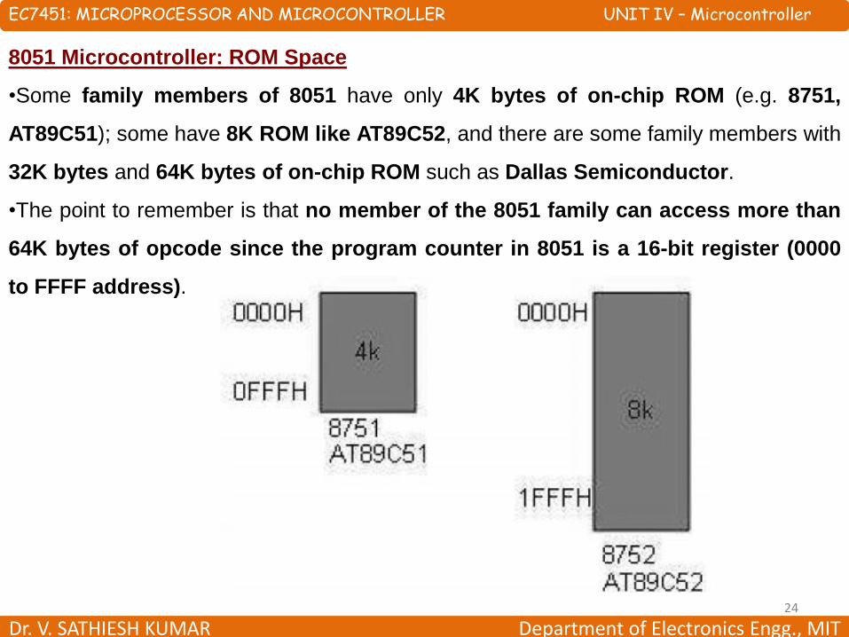
8051 Microcontroller: ROM Space
•Some family members of 8051 have only 4K bytes of on-chip ROM (e.g. 8751,
AT89C51); some have 8K ROM like AT89C52, and there are some family members with
32K bytes and 64K bytes of on-chip ROM such as Dallas Semiconductor.
•The point to remember is that no member of the 8051 family can access more than
64K bytes of opcode since the program counter in 8051 is a 16-bit register (0000
to FFFF address).

EC7451: MICROPROCESSOR AND MICROCONTROLLER UNIT IV – Microcontroller
Dr. V. SATHIESH KUMAR Department of Electronics Engg., MIT25
8051 Microcontroller: Reset Vector
•The significance of the reset vector (0000H in ROM) is that it points the processor to
the memory address which contains the firmware's first instruction.
•Without the Reset Vector, the processor would not know where to begin execution.
•Upon RESET, the processor loads the Program Counter (PC) with the reset vector
value from a predefined memory location.
EC7451: MICROPROCESSOR AND MICROCONTROLLER UNIT IV – Microcontroller
Dr. V. SATHIESH KUMAR Department of Electronics Engg., MIT26
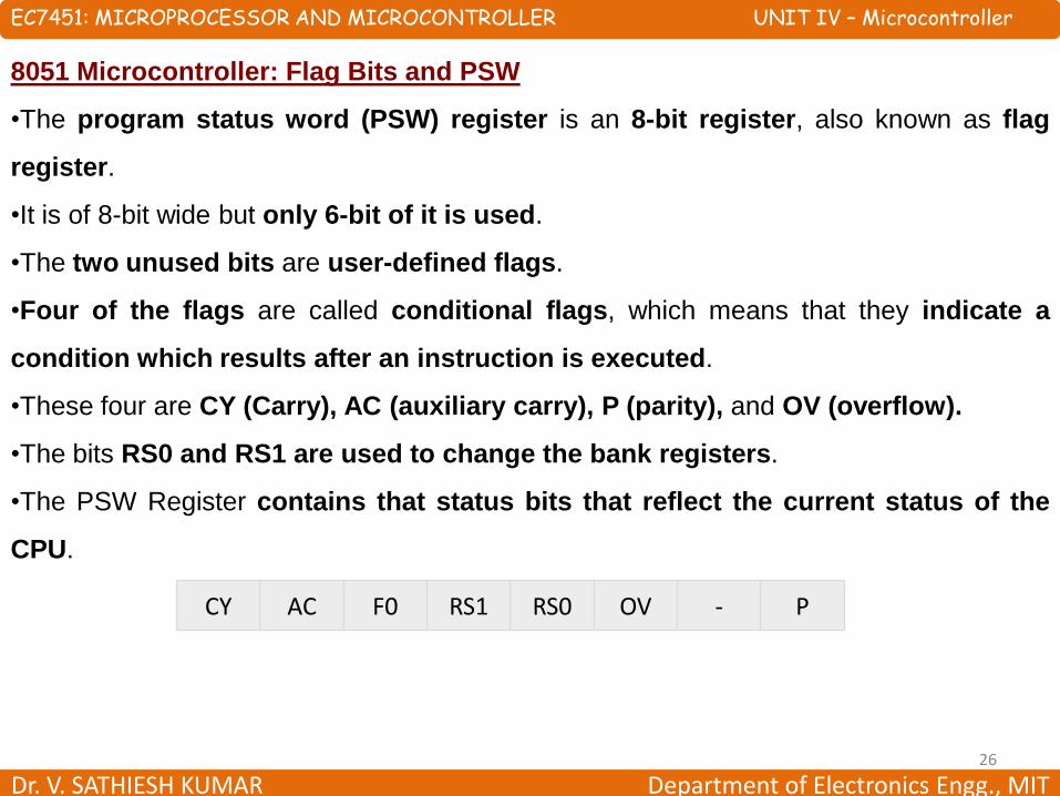
8051 Microcontroller: Flag Bits and PSW
•The program status word (PSW) register is an 8-bit register, also known as flag
register.
•It is of 8-bit wide but only 6-bit of it is used.
•The two unused bits are user-defined flags.
•Four of the flags are called conditional flags, which means that they indicate a
condition which results after an instruction is executed.
•These four are CY (Carry), AC (auxiliary carry), P (parity), and OV (overflow).
•The bits RS0 and RS1 are used to change the bank registers.
•The PSW Register contains that status bits that reflect the current status of the
CPU.
CY AC F0 RS1 RS0 OV - P

EC7451: MICROPROCESSOR AND MICROCONTROLLER UNIT IV – Microcontroller
Dr. V. SATHIESH KUMAR Department of Electronics Engg., MIT27
8051 Microcontroller: Flag Bits and PSW
CY PSW.7 Carry Flag
AC PSW.6 Auxiliary Carry Flag
F0 PSW.5 Flag 0 available to user for general purpose.
RS1 PSW.4 Register Bank selector bit 1
RS0 PSW.3 Register Bank selector bit 0
OV PSW.2 Overflow Flag
- PSW.1 User definable FLAG
P PSW.0 Parity FLAG. Set/ cleared by hardware during instruction cycle to indicate even/odd number of 1 bit in accumulator.

EC7451: MICROPROCESSOR AND MICROCONTROLLER UNIT IV – Microcontroller
Dr. V. SATHIESH KUMAR Department of Electronics Engg., MIT28
8051 Microcontroller: Flag Bits and PSW
•We can select the corresponding Register Bank select bit using RS0 and RS1 bits.
CY, the carry flag : This carry flag is set (1) whenever there is a carry out from the
D7 bit.
•It is affected after an 8-bit addition or subtraction operation.
•It can also be reset to 1 or 0 directly by an instruction such as "SETB C" and "CLR C"
where "SETB" stands for set bit carry and "CLR" stands for clear carry.
RS1 RS0 Register Bank Address
0 0 0 00H-07H
0 1 1 08H-0FH
1 0 2 10H-17H
1 1 3 18H-1FH
EC7451: MICROPROCESSOR AND MICROCONTROLLER UNIT IV – Microcontroller
Dr. V. SATHIESH KUMAR Department of Electronics Engg., MIT29
8051 Microcontroller: Flag Bits and PSW
AC, auxiliary carry flag : If there is a carry from D3 and D4 during an ADD or SUB
operation, the AC bit is set; otherwise, it is cleared.
•It is used for the instruction to perform binary coded decimal arithmetic.
P, the parity flag : The parity flag represents the number of 1's in the accumulator
register only.
•If the A register contains odd number of 1's, then P = 1; and for even number of 1's,
P = 0.
OV, the overflow flag : This flag is set whenever the result of a signed number
operation is too large causing the high-order bit to overflow into the sign bit.
•It is used only to detect errors in signed arithmetic operations.

EC7451: MICROPROCESSOR AND MICROCONTROLLER UNIT IV – Microcontroller
Dr. V. SATHIESH KUMAR Department of Electronics Engg., MIT30
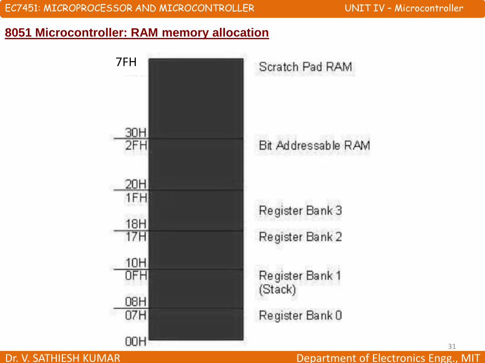
8051 Microcontroller: RAM memory allocation
•The 8051 microcontroller has a total of 128 bytes of RAM.
•The 128 bytes of RAM inside the 8051 are assigned the address 00 to 7FH.
•They can be accessed directly as memory locations and are divided into three
different groups as follows,
1. 32 bytes from 00H to 1FH locations are set aside for register banks and the
stack.
2. 16 bytes from 20H to 2FH locations are set aside for bit-addressable read/write
memory.
3. 80 bytes from 30H to 7FH locations are used for read and write storage; it is
called as scratch pad. These 80 locations RAM are widely used for the purpose
of storing data and parameters by 8051 programmers.
EC7451: MICROPROCESSOR AND MICROCONTROLLER UNIT IV – Microcontroller
Dr. V. SATHIESH KUMAR Department of Electronics Engg., MIT31
8051 Microcontroller: RAM memory allocation
7FH

EC7451: MICROPROCESSOR AND MICROCONTROLLER UNIT IV – Microcontroller
Dr. V. SATHIESH KUMAR Department of Electronics Engg., MIT32
8051 Microcontroller: RAM memory allocation
Register Banks in 8051:
•A total of 32 bytes of RAM are set aside for the register banks and the stack.
•These 32 bytes are divided into four register banks in which each bank has 8
registers, R0–R7.
•RAM locations from 00H to 07H are set aside for bank 0 of R0–R7 where R0 is RAM
location 00, R1 is RAM location 01, R2 is location 02, and so on, until the memory
location 07, which belongs to R7 of bank 0.
•The second bank of registers R0–R7 starts at RAM location 08H and goes to
locations 0FH.
•The third bank of R0–R7 starts at memory location 10H and goes to location to
17H.
• Finally, RAM locations 18H to 1FH are set aside for the fourth bank of R0–R7.
EC7451: MICROPROCESSOR AND MICROCONTROLLER UNIT IV – Microcontroller
Dr. V. SATHIESH KUMAR Department of Electronics Engg., MIT33
8051 Microcontroller: RAM memory allocation
Default Register Bank:
•If RAM locations 00–1F are set aside for the four registers banks, which register bank
of R0–R7 do we have access to when the 8051 is powered up?
•The answer is register bank 0; that is, RAM locations from 0 to 7 are accessed with
the names R0 to R7 when programming the 8051.
•Because it is much easier to refer these RAM locations by names such as R0 to
R7, rather than by their memory locations.
EC7451: MICROPROCESSOR AND MICROCONTROLLER UNIT IV – Microcontroller
Dr. V. SATHIESH KUMAR Department of Electronics Engg., MIT34
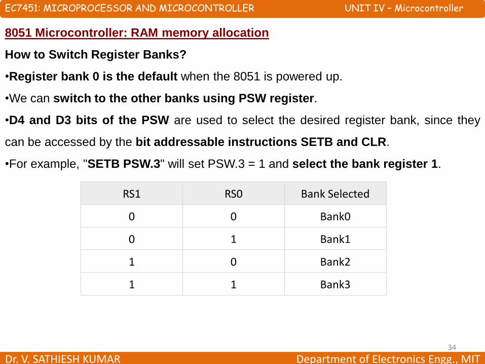
8051 Microcontroller: RAM memory allocation
How to Switch Register Banks?
•Register bank 0 is the default when the 8051 is powered up.
•We can switch to the other banks using PSW register.
•D4 and D3 bits of the PSW are used to select the desired register bank, since they
can be accessed by the bit addressable instructions SETB and CLR.
•For example, "SETB PSW.3" will set PSW.3 = 1 and select the bank register 1.
RS1 RS0 Bank Selected
0 0 Bank0
0 1 Bank1
1 0 Bank2
1 1 Bank3

EC7451: MICROPROCESSOR AND MICROCONTROLLER UNIT IV – Microcontroller
Dr. V. SATHIESH KUMAR Department of Electronics Engg., MIT35
8051 Microcontroller: RAM memory allocation
Stack and its Operations:
•The stack is a section of a RAM used by the CPU to store information such as data
or memory address on temporary basis.
•The CPU needs this storage area considering limited number of registers.
How Stacks are Accessed?
•As the stack is a section of a RAM, there are registers inside the CPU to point to it.
•The register used to access the stack is known as the stack pointer register.
•The stack pointer in the 8051 is 8-bits wide, and it can take a value of 00H to FFH.
•When the 8051 is initialized, the SP register contains the value 07H. This means
that the RAM location 08 is the first location used for the stack.
•The storing operation of a CPU register in the stack is known as a PUSH, and
getting the contents from the stack back into a CPU register is called a POP.
EC7451: MICROPROCESSOR AND MICROCONTROLLER UNIT IV – Microcontroller
Dr. V. SATHIESH KUMAR Department of Electronics Engg., MIT36
8051 Microcontroller: RAM memory allocation
Pushing into the Stack:
•In the 8051, the stack pointer (SP) points to the last used location of the stack.
•When data is pushed onto the stack, the stack pointer (SP) is incremented by 1.
•When PUSH is executed, the contents of the register are saved on the stack and
SP is incremented by 1.
•To push the registers onto the stack, we must use their RAM addresses.
•For example, the instruction "PUSH 1" pushes register R1 onto the stack.
Popping from the Stack:
•Popping the contents of the stack back into a given register is the opposite to the
process of pushing.
•With every pop operation, the top byte of the stack is copied to the register
specified by the instruction and the stack pointer is decremented once.

Dr. V. SATHIESH KUMAR Department of Electronics Engg., MIT37
External Memory Interface with 8051:
The 8051 microcontroller has the internal program memory.
In this chip, there is EA pin. It indicates the External Access.
So by using this pin, we can check whether the internal program memory is used
or not.
So when there is a low signal in this pin, the internal 4K bytes of program memory
is not used, but in this situation, it can access only the ROM.
When we are trying to access the external data memory, then the read RD or
write WR will be the output from 8051.
So for reading the data from external sources, there PSEN (Program Strobe
Enable) pin. This is an active low output pin.
When this pin is active low, it indicates that the microcontroller reads from the
external ROM.
The 16-bit ROM address will be floated on Port 2 (MS Byte) and Port 0 (LS Byte).
The program code is received on Port 0 pins.
EC7451: MICROPROCESSOR AND MICROCONTROLLER UNIT IV – Microcontroller

Dr. V. SATHIESH KUMAR Department of Electronics Engg., MIT38
External Memory Interface with 8051:
So there is two case of accessing the program memory.
The first case is when EA is low, and the second case is when EA is high.
For the low state of EA, it can access the entire external memory from location
0000H to FFFFH.
And in the second case (EA = 1). In this case, the internal memory is accessed by
the address 0000H to 0FFFH. And also the external memory is accessed from
location 1000H to FFFFH.
EC7451: MICROPROCESSOR AND MICROCONTROLLER UNIT IV – Microcontroller
Dr. V. SATHIESH KUMAR Department of Electronics Engg., MIT39
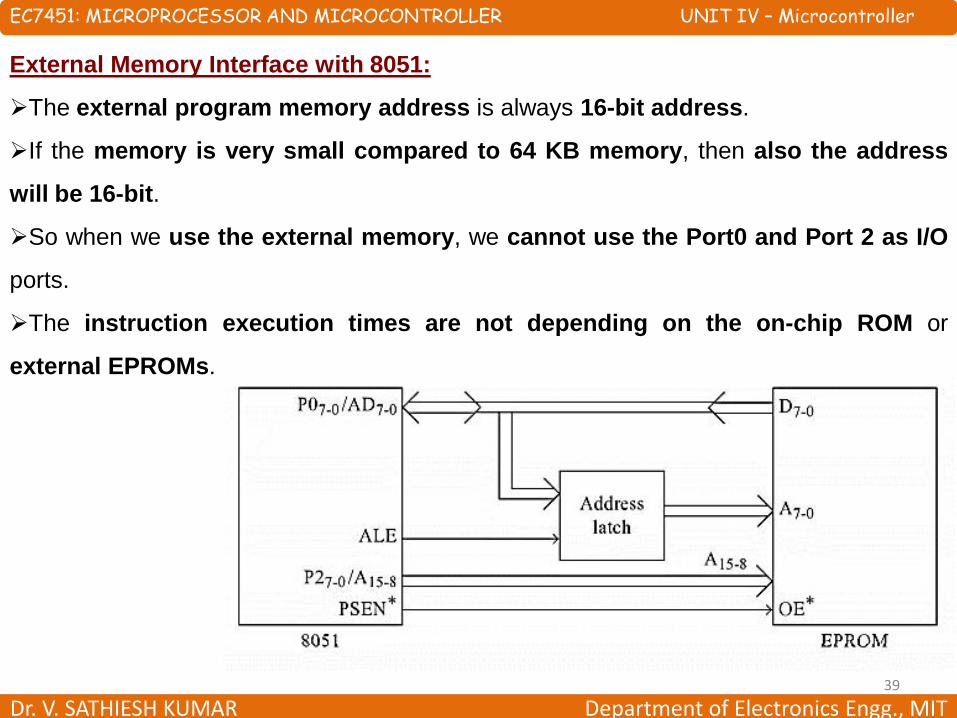
External Memory Interface with 8051:
The external program memory address is always 16-bit address.
If the memory is very small compared to 64 KB memory, then also the address
will be 16-bit.
So when we use the external memory, we cannot use the Port0 and Port 2 as I/O
ports.
The instruction execution times are not depending on the on-chip ROM or
external EPROMs.
EC7451: MICROPROCESSOR AND MICROCONTROLLER UNIT IV – Microcontroller

EC7451: MICROPROCESSOR AND MICROCONTROLLER UNIT IV – Microcontroller
Dr. V. SATHIESH KUMAR Department of Electronics Engg., MIT40
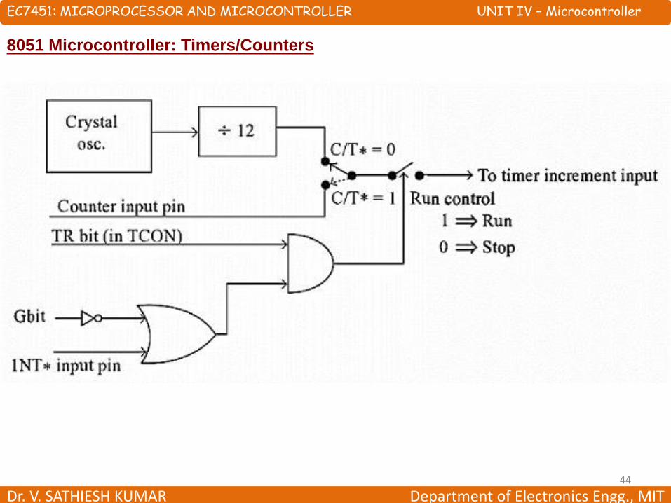
8051 Microcontroller: Timers/Counters
•In Intel 8051, there are two 16-bit timer registers. These registers are known as
Timer0 and Timer1.
•The timer registers can be used in two modes,
1. Timer mode
2. Counter mode
•The only difference between these two modes is the source for incrementing the
timer registers.
Timer Mode:
•In the timer mode, the internal machine cycles are counted. So this register is
incremented in each machine cycle.
•So when the clock frequency is 12 MHz, then the timer register is incremented in
each millisecond.
•In this mode it ignores the external timer input pin.
EC7451: MICROPROCESSOR AND MICROCONTROLLER UNIT IV – Microcontroller
Dr. V. SATHIESH KUMAR Department of Electronics Engg., MIT41
8051 Microcontroller: Timers/Counters
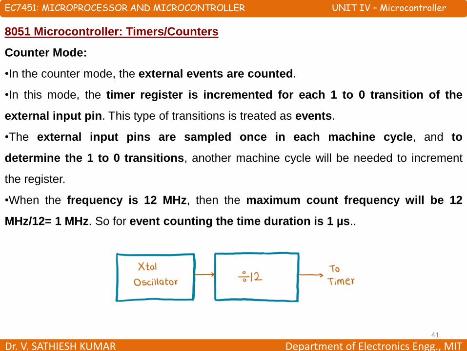
Counter Mode:
•In the counter mode, the external events are counted.
•In this mode, the timer register is incremented for each 1 to 0 transition of the
external input pin. This type of transitions is treated as events.
•The external input pins are sampled once in each machine cycle, and to
determine the 1 to 0 transitions, another machine cycle will be needed to increment
the register.
•When the frequency is 12 MHz, then the maximum count frequency will be 12
MHz/12= 1 MHz. So for event counting the time duration is 1 µs..
EC7451: MICROPROCESSOR AND MICROCONTROLLER UNIT IV – Microcontroller
Dr. V. SATHIESH KUMAR Department of Electronics Engg., MIT42
8051 Microcontroller: Timers/Counters
•There are four different modes of the Timer or Counter.
•The Mode 0 to Mode 2 are for both of the Timer/Counter.
•Mode 3 has a different meaning for each timer register.
•There is a register called TMOD. This register can be programmed to configure these
timers or counters.
•The Serial port is used for serial communication in mode 1 and 3.
•Timer1 is used for generating the baud rate.
•So only Timer0 is available for timer or counter operations.
EC7451: MICROPROCESSOR AND MICROCONTROLLER UNIT IV – Microcontroller
Dr. V. SATHIESH KUMAR Department of Electronics Engg., MIT43
8051 Microcontroller: Timers/Counters
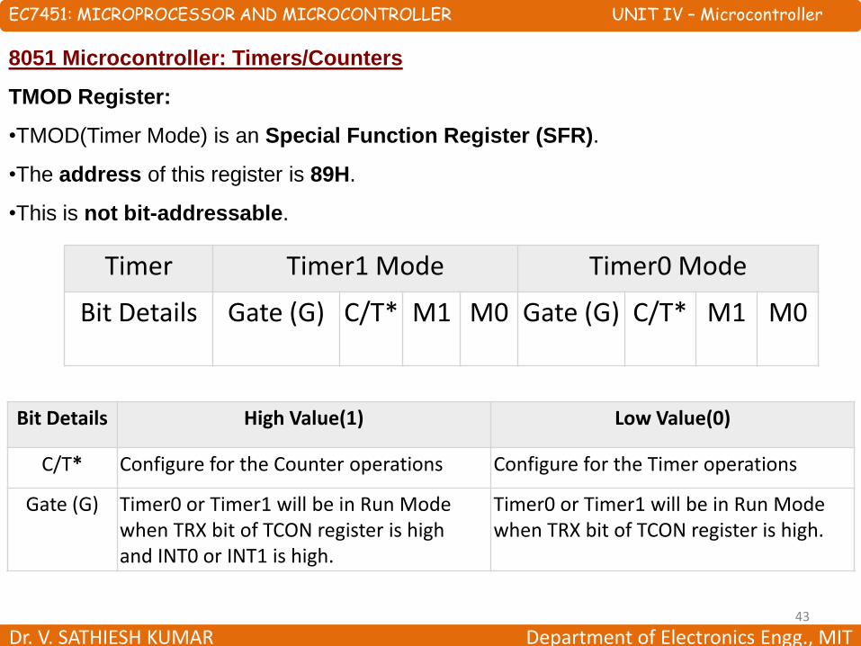
TMOD Register:
•TMOD(Timer Mode) is an Special Function Register (SFR).
•The address of this register is 89H.
•This is not bit-addressable.
Timer Timer1 Mode Timer0 Mode
Bit Details Gate (G) C/T* M1 M0 Gate (G) C/T* M1 M0
Bit Details High Value(1) Low Value(0)
C/T* Configure for the Counter operations Configure for the Timer operations
Gate (G) Timer0 or Timer1 will be in Run Mode when TRX bit of TCON register is high and INT0 or INT1 is high.
Timer0 or Timer1 will be in Run Mode when TRX bit of TCON register is high.
EC7451: MICROPROCESSOR AND MICROCONTROLLER UNIT IV – Microcontroller
Dr. V. SATHIESH KUMAR Department of Electronics Engg., MIT44
8051 Microcontroller: Timers/Counters

EC7451: MICROPROCESSOR AND MICROCONTROLLER UNIT IV – Microcontroller
Dr. V. SATHIESH KUMAR Department of Electronics Engg., MIT45
8051 Microcontroller: Timers/Counters
M1 M0 Mode Operation
0 0 0 (13-bit timer mode) 13-bit timer/counter, 8-bit of THx & 5-bit of TLx
0 1 1 (16-bit timer mode) 16-bit timer/counter, THx cascaded with TLx
1 0 2 (8-bit auto reload mode)
8-bit timer/counter (auto reload mode), TLx
reload with value held by THx each time TLx
overflow
1 1 3 (split timer mode)
Timer 0: Split 16-bit timer X two 8-bit timer i.e.
THx and TLx like two 8-bit timer
Timer 1: used for Baud Rate generation in Serial
Communication
EC7451: MICROPROCESSOR AND MICROCONTROLLER UNIT IV – Microcontroller
Dr. V. SATHIESH KUMAR Department of Electronics Engg., MIT46
8051 Microcontroller: Timers/Counters
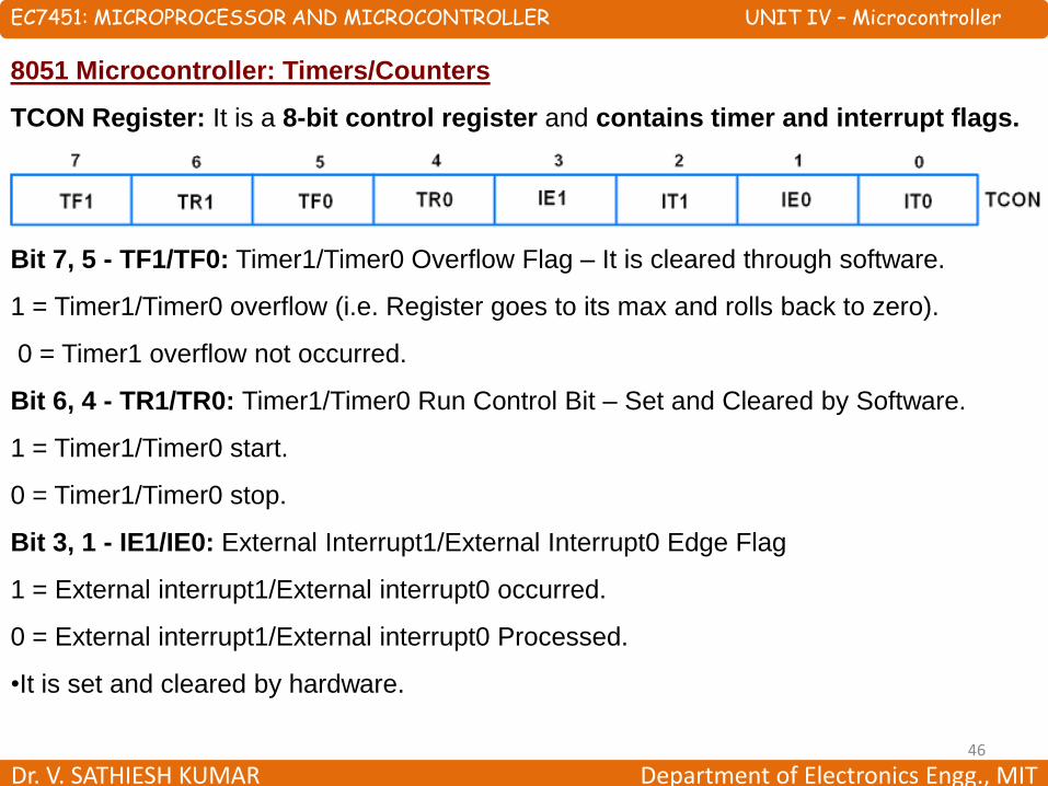
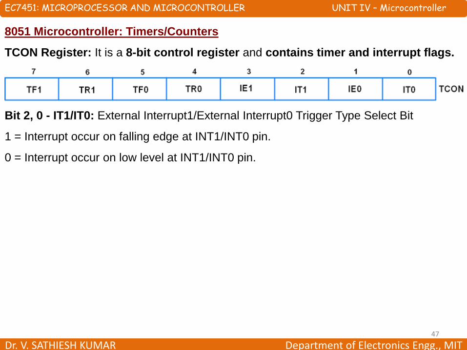
TCON Register: It is a 8-bit control register and contains timer and interrupt flags.
Bit 7, 5 - TF1/TF0: Timer1/Timer0 Overflow Flag – It is cleared through software.
1 = Timer1/Timer0 overflow (i.e. Register goes to its max and rolls back to zero).
0 = Timer1 overflow not occurred.
Bit 6, 4 - TR1/TR0: Timer1/Timer0 Run Control Bit – Set and Cleared by Software.
1 = Timer1/Timer0 start.
0 = Timer1/Timer0 stop.
Bit 3, 1 - IE1/IE0: External Interrupt1/External Interrupt0 Edge Flag
1 = External interrupt1/External interrupt0 occurred.
0 = External interrupt1/External interrupt0 Processed.
•It is set and cleared by hardware.
EC7451: MICROPROCESSOR AND MICROCONTROLLER UNIT IV – Microcontroller
Dr. V. SATHIESH KUMAR Department of Electronics Engg., MIT47
8051 Microcontroller: Timers/Counters
TCON Register: It is a 8-bit control register and contains timer and interrupt flags.
Bit 2, 0 - IT1/IT0: External Interrupt1/External Interrupt0 Trigger Type Select Bit
1 = Interrupt occur on falling edge at INT1/INT0 pin.
0 = Interrupt occur on low level at INT1/INT0 pin.

EC7451: MICROPROCESSOR AND MICROCONTROLLER UNIT IV – Microcontroller
Dr. V. SATHIESH KUMAR Department of Electronics Engg., MIT48
8051 Microcontroller: Timers/Counter Modes
Mode 0 (13-bit timer mode):
•Mode 0 is 13-bit timer mode for which 8-bit of THx and 5-bit of TLx (as Prescaler)
are used.
•As shown in above figure, 8-bit of THx and lower 5-bit of TLx used to form a total 13-bit
timer.
•Higher 3-bits of TLx should be written as zero while using timer mode0, or it will
affect the result.

EC7451: MICROPROCESSOR AND MICROCONTROLLER UNIT IV – Microcontroller
Dr. V. SATHIESH KUMAR Department of Electronics Engg., MIT49
8051 Microcontroller: Timers/Counter Modes
Mode 1 (16-bit timer mode):
•Mode 1 is 16-bit timer mode used to generate a delay, it uses 8-bit of THx and 8-bit
of TLx to form a total 16-bit register.

EC7451: MICROPROCESSOR AND MICROCONTROLLER UNIT IV – Microcontroller
Dr. V. SATHIESH KUMAR Department of Electronics Engg., MIT50
8051 Microcontroller: Timers/Counter Modes
Mode 2 (8-bit auto-reload timer mode):
•Mode 2 is 8-bit auto-reload timer mode.
•In this mode we have to load the THx-8 bit value only.
•When the Timer gets started, THx value gets automatically loaded into the TLx
and TLx starts counting from that value.
•After the value of TLx overflows from the 0xFF to 0x00, the TFx flag gets set and
again value from the THx gets automatically loaded into the TLx register.
EC7451: MICROPROCESSOR AND MICROCONTROLLER UNIT IV – Microcontroller
Dr. V. SATHIESH KUMAR Department of Electronics Engg., MIT51
8051 Microcontroller: Timers/Counter Modes
Mode 3 (Split timer mode):
•Mode 3 is different for Timer0 and Timer1.
•When the Timer0 is working in mode 3, the TL0 will be used as an 8-bit
timer/counter.
•It will be controlled by the standard Timer0 control bits.
•The TH0 is used as an 8-bit timer but not the counter. This is controlled by Timer1
Control bit TR1.
•When the TH0 overflows from FFH to 00H, then TF1 is set to 1.
•When the Timer1 is working in Mode 3, it simply holds the count but does not run.
•When Timer0 is in mode 3, the Timer1 is configured in one of the mode 0, 1 and 2.
•In this case, the Timer1 cannot interrupt the microcontroller.
•When the TF1 is used by TH0 timer, the Timer1 is used as Baud Rate Generator.

EC7451: MICROPROCESSOR AND MICROCONTROLLER UNIT IV – Microcontroller
Dr. V. SATHIESH KUMAR Department of Electronics Engg., MIT52
8051 Microcontroller: Timers/Counter Modes
EC7451: MICROPROCESSOR AND MICROCONTROLLER UNIT IV – Microcontroller
Dr. V. SATHIESH KUMAR Department of Electronics Engg., MIT53
8051 Microcontroller: Interrupts
• Interrupts are basically the events that temporarily suspend the main program, pass
the control to the external sources and execute their task. It then passes the
control to the main program where it had left off.
•8051 has five interrupts. These interrupts are INT0*, INT1*,T0 ,T1 and TI/RI.
•All of the interrupts can be enabled or disabled by using the IE (interrupt enable)
register.
•The interrupt addresses of these interrupts are like below,
Interrupt Address
INT0* 0003H
INT1* 000BH
T0 0013H
T1 001BH
TI/RI 0023H

EC7451: MICROPROCESSOR AND MICROCONTROLLER UNIT IV – Microcontroller
Dr. V. SATHIESH KUMAR Department of Electronics Engg., MIT54
8051 Microcontroller: Interrupts
Interrupt Enable (IE) Register:
•This register can be used to enable or disable interrupts programmatically.
•This register is an SFR.
•The address is A8H.
•This byte is bit addressable.
•So it can be programmed by the user.
Bit Address AF AE AD AC AB AA A9 A8
Bit Details EA X X ES ET1 EX1 ET0 EX0
Bit Details High Value(1) Low Value(0)
EA Least significant 5 bits can decide enable or disable of these five interrupts.
Disable all five interrupts. It just ignores the rest five bits.
ES Enable Serial Port Interrupt Disable Serial Port Interrupt
ET1 Enable Timer1 interrupt Disable Timer1 interrupt
EX1 Enable external interrupt 1 (INT1*) Disable external interrupt 1 (INT1*)
ET0 Enable Timer0 interrupt Disable Timer0 interrupt
EX0 Enable external interrupt 0 (INT0*) Disable external interrupt 0 (INT0*)
EC7451: MICROPROCESSOR AND MICROCONTROLLER UNIT IV – Microcontroller
Dr. V. SATHIESH KUMAR Department of Electronics Engg., MIT55
8051 Microcontroller: Interrupts
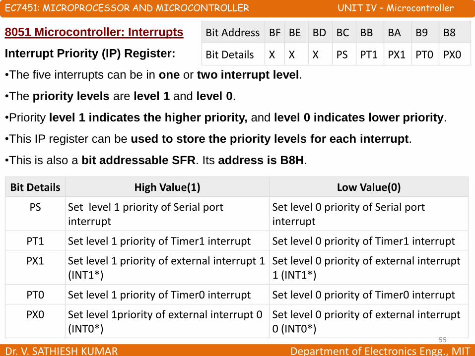
Interrupt Priority (IP) Register:
•The five interrupts can be in one or two interrupt level.
•The priority levels are level 1 and level 0.
•Priority level 1 indicates the higher priority, and level 0 indicates lower priority.
•This IP register can be used to store the priority levels for each interrupt.
•This is also a bit addressable SFR. Its address is B8H.
Bit Address BF BE BD BC BB BA B9 B8
Bit Details X X X PS PT1 PX1 PT0 PX0
Bit Details High Value(1) Low Value(0)
PS Set level 1 priority of Serial port interrupt
Set level 0 priority of Serial port interrupt
PT1 Set level 1 priority of Timer1 interrupt Set level 0 priority of Timer1 interrupt
PX1 Set level 1 priority of external interrupt 1 (INT1*)
Set level 0 priority of external interrupt 1 (INT1*)
PT0 Set level 1 priority of Timer0 interrupt Set level 0 priority of Timer0 interrupt
PX0 Set level 1priority of external interrupt 0 (INT0*)
Set level 0 priority of external interrupt 0 (INT0*)
EC7451: MICROPROCESSOR AND MICROCONTROLLER UNIT IV – Microcontroller
Dr. V. SATHIESH KUMAR Department of Electronics Engg., MIT56
8051 Microcontroller: Interrupts
EC7451: MICROPROCESSOR AND MICROCONTROLLER UNIT IV – Microcontroller
Dr. V. SATHIESH KUMAR Department of Electronics Engg., MIT57
8051 Microcontroller: Interrupts
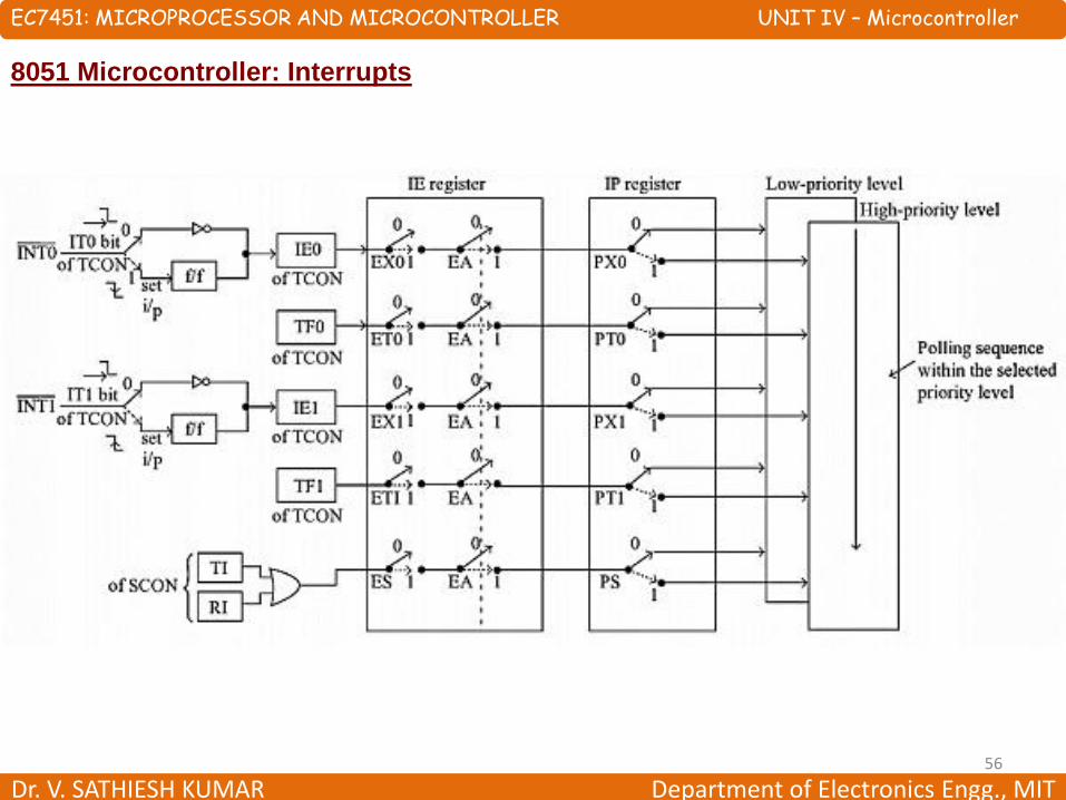
•When all of the five interrupts are in same priority level, and if all of the interrupts
are enabled, then the sequence of interrupts will be INT0*, T0, INT1*, T1, TI/R I.
•Some specific priority register value can be used to maintain the priorities of the
interrupts.
•Let the value of Priority register is xxx00101 indicates the sequence INT0*, INT1*,
TI/RI, T1, T0.
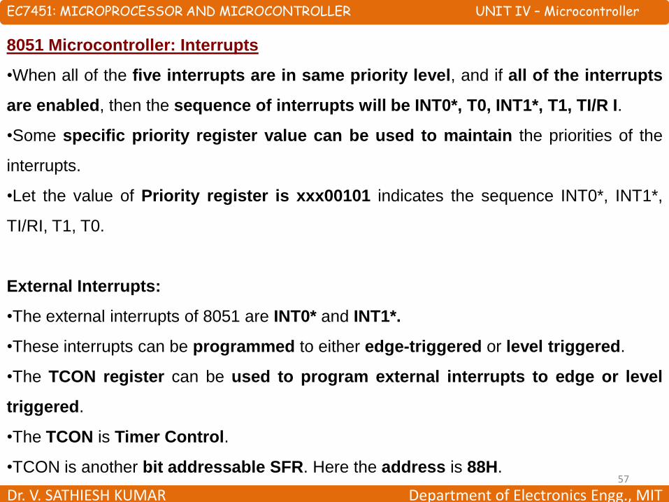
External Interrupts:
•The external interrupts of 8051 are INT0* and INT1*.
•These interrupts can be programmed to either edge-triggered or level triggered.
•The TCON register can be used to program external interrupts to edge or level
triggered.
•The TCON is Timer Control.
•TCON is another bit addressable SFR. Here the address is 88H.
EC7451: MICROPROCESSOR AND MICROCONTROLLER UNIT IV – Microcontroller
Dr. V. SATHIESH KUMAR Department of Electronics Engg., MIT58
8051 Microcontroller: Interrupts
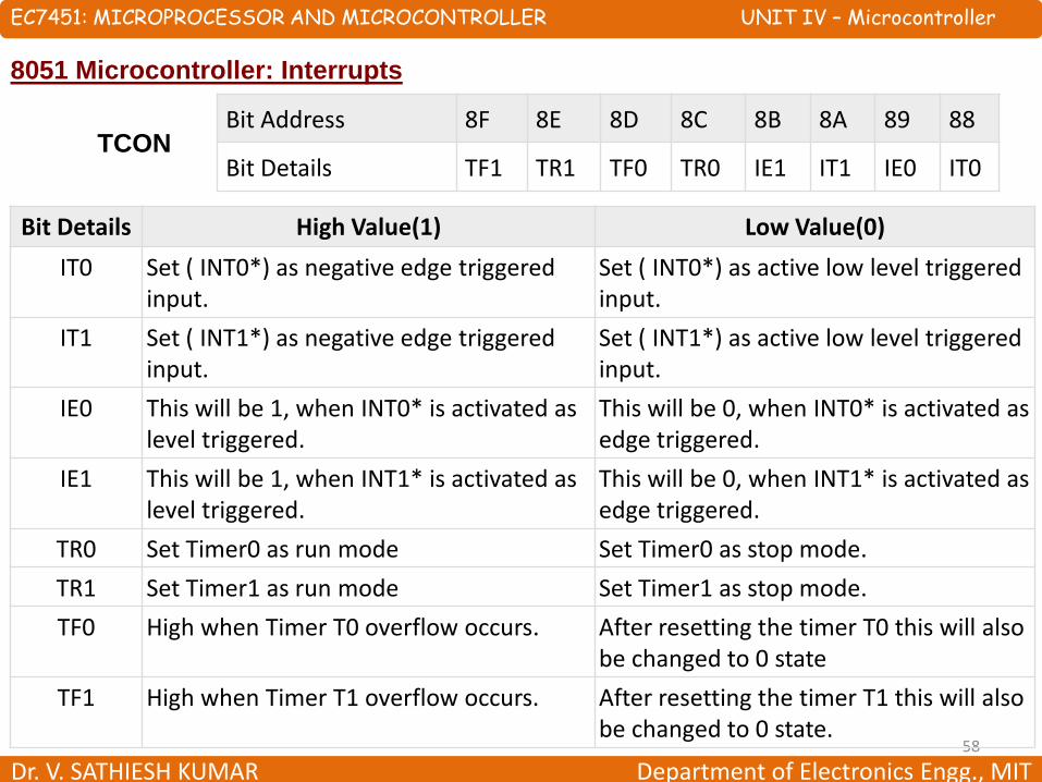
Bit Address 8F 8E 8D 8C 8B 8A 89 88
Bit Details TF1 TR1 TF0 TR0 IE1 IT1 IE0 IT0
Bit Details High Value(1) Low Value(0)
IT0 Set ( INT0*) as negative edge triggered input.
Set ( INT0*) as active low level triggered input.
IT1 Set ( INT1*) as negative edge triggered input.
Set ( INT1*) as active low level triggered input.
IE0 This will be 1, when INT0* is activated as level triggered.
This will be 0, when INT0* is activated as edge triggered.
IE1 This will be 1, when INT1* is activated as level triggered.
This will be 0, when INT1* is activated as edge triggered.
TR0 Set Timer0 as run mode Set Timer0 as stop mode.
TR1 Set Timer1 as run mode Set Timer1 as stop mode.
TF0 High when Timer T0 overflow occurs. After resetting the timer T0 this will also be changed to 0 state
TF1 High when Timer T1 overflow occurs. After resetting the timer T1 this will also be changed to 0 state.
TCON

EC7451: MICROPROCESSOR AND MICROCONTROLLER UNIT IV – Microcontroller
Dr. V. SATHIESH KUMAR Department of Electronics Engg., MIT59
8051 Microcontroller: Interrupts
•The IT0 and IT1 are stands for Interrupt Type. These bits are used to decide whether
the INT0* and INT1* will be level trigged or edge triggered.
•IE0 and IE1 bits are used to indicate the status of external interrupts. These bit can
be set or reset by the microcontroller itself.
•The first four bits are the status information about timers.
•When TR0 and TR1 are 1, it indicates the running mode of the timers. These bits
provide software control over the running of timers. Timers can also be controlled by the
hardware. The priority of hardware mode is higher than the software mode.
•The TF0 and TF1 are used to indicate the overflow of timer T0 and T1, respectively.
•When overflow occurs these flags are set to 1.
•When the interrupt is handled by some interrupt service subroutine (ISS), these will be
0.
EC7451: MICROPROCESSOR AND MICROCONTROLLER UNIT IV – Microcontroller
Dr. V. SATHIESH KUMAR Department of Electronics Engg., MIT60
8051 Microcontroller: Interrupts
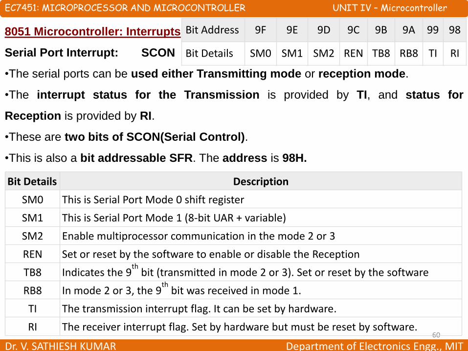
Serial Port Interrupt:
•The serial ports can be used either Transmitting mode or reception mode.
•The interrupt status for the Transmission is provided by TI, and status for
Reception is provided by RI.
•These are two bits of SCON(Serial Control).
•This is also a bit addressable SFR. The address is 98H.
Bit Address 9F 9E 9D 9C 9B 9A 99 98
Bit Details SM0 SM1 SM2 REN TB8 RB8 TI RI
Bit Details Description
SM0 This is Serial Port Mode 0 shift register
SM1 This is Serial Port Mode 1 (8-bit UAR + variable)
SM2 Enable multiprocessor communication in the mode 2 or 3
REN Set or reset by the software to enable or disable the Reception
TB8 Indicates the 9th
bit (transmitted in mode 2 or 3). Set or reset by the software
RB8 In mode 2 or 3, the 9th
bit was received in mode 1.
TI The transmission interrupt flag. It can be set by hardware.
RI The receiver interrupt flag. Set by hardware but must be reset by software.
SCON

Dr. V. SATHIESH KUMAR Department of Electronics Engg., MIT61
8051 Microcontroller: Serial Communication
•One of the 8051s many powerful features is its integrated UART, otherwise known as
a serial port.
•We need to configure the serial ports operation mode and baud rate.
•Once configured, all we have to do is write to an SFR to write a value to the serial
port or read the same SFR to read a value from the serial port.
•The 8051 will automatically let us know when it has finished sending the character
we wrote and will also let us know whenever it has received a byte so that we can
process it.
EC7451: MICROPROCESSOR AND MICROCONTROLLER UNIT IV – Microcontroller

Dr. V. SATHIESH KUMAR Department of Electronics Engg., MIT62
8051 Microcontroller: Serial Communication – Configuration
•This lets us tell the 8051 how many data bits we want, the baud rate we will be using,
and how the baud rate will be determined.
•"Serial Control" (SCON) SFR represents,
MICROPROCESSOR AND MICROCONTROLLER UNIT IV & V – Microcontroller & it Applications
Bit Name Bit Address Explanation of Function
7 SM0 9FH Serial port mode bit 0
6 SM1 9EH Serial port mode bit 1.
5 SM2 9DH Multiprocessor Communications Enable
4 REN 9CHReceiver Enable. This bit must be set in order to receive
characters.
3 TB8 9BH Transmit bit 8. The 9th bit to transmit in mode 2 and 3.
2 RB8 9AH Receive bit 8. The 9th bit received in mode 2 and 3.
1 TI 99HTransmit Flag. Set when a byte has been completely
transmitted.
0 RI 98H Receive Flag. Set when a byte has been completely received.
Bit Address 9F 9E 9D 9C 9B 9A 99 98
Bit Details SM0 SM1 SM2 REN TB8 RB8 TI RI
Dr. V. SATHIESH KUMAR Department of Electronics Engg., MIT63
8051 Microcontroller: Serial Communication – Configuration
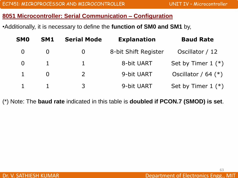
•Additionally, it is necessary to define the function of SM0 and SM1 by,
(*) Note: The baud rate indicated in this table is doubled if PCON.7 (SMOD) is set.
SM0 SM1 Serial Mode Explanation Baud Rate
0 0 0 8-bit Shift Register Oscillator / 12
0 1 1 8-bit UART Set by Timer 1 (*)
1 0 2 9-bit UART Oscillator / 64 (*)
1 1 3 9-bit UART Set by Timer 1 (*)
EC7451: MICROPROCESSOR AND MICROCONTROLLER UNIT IV – Microcontroller
Dr. V. SATHIESH KUMAR Department of Electronics Engg., MIT64
8051 Microcontroller: Serial Communication – Configuration
•The first four bits (bits 4 through 7) are configuration bits.
•Bits SM0 and SM1 let us set the serial mode to a value between 0 and 3, inclusive.
Selecting the Serial Mode selects the mode of operation (8-bit/9-bit, UART or Shift
Register) and also determines how the baud rate will be calculated.
In modes 0 and 2 the baud rate is fixed based on the oscillators frequency.
In modes 1 and 3 the baud rate is variable based on how often Timer 1 overflows.
• The next bit, SM2, is a flag for "Multiprocessor communication."
Generally, whenever a byte has been received the 8051 will set the "RI" (Receive
Interrupt) flag. This lets the program know that a byte has been received.
However, when SM2 is set, the "RI" flag will only be triggered if the 9th bit
received was a "1". That is to say, if SM2 is set and a byte is received whose 9th bit is
clear, the RI flag will never be set. This can be useful in certain advanced serial
applications.
EC7451: MICROPROCESSOR AND MICROCONTROLLER UNIT IV – Microcontroller
Dr. V. SATHIESH KUMAR Department of Electronics Engg., MIT65
8051 Microcontroller: Serial Communication – Configuration
•The next bit, REN, is "Receiver Enable.“
If you want to receive data via the serial port, set this bit.
You will almost always want to set this bit.
•The last four bits (bits 0 through 3) are operational bits. They are used when actually
sending and receiving data--they are not used to configure the serial port.
•The TB8 bit is used in modes 2 and 3.
In modes 2 and 3, a total of nine data bits are transmitted.
The first 8 data bits are the 8 bits of the main value, and the ninth bit is taken from
TB8.
If TB8 is set and a value is written to the serial port, the data bits will be written to
the serial line followed by a "set" ninth bit. If TB8 is clear the ninth bit will be "clear.”
EC7451: MICROPROCESSOR AND MICROCONTROLLER UNIT IV – Microcontroller
Dr. V. SATHIESH KUMAR Department of Electronics Engg., MIT66
8051 Microcontroller: Serial Communication – Configuration
•The RB8 also operates in modes 2 and 3 and functions essentially the same way as
TB8, but on the reception side.
When a byte is received in modes 2 or 3, a total of nine bits are received.
In this case, the first eight bits received are the data of the serial byte received
and the value of the ninth bit received will be placed in RB8.
•TI means "Transmit Interrupt."
When a program writes a value to the serial port, a certain amount of time will
pass before the individual bits of the byte are "clocked out" the serial port.
The 8051 lets the program know that it has "clocked out" the last byte by setting
the TI bit.
When the TI bit is set, the program may assume that the serial port is "free" and ready
to send the next byte.
EC7451: MICROPROCESSOR AND MICROCONTROLLER UNIT IV – Microcontroller
Dr. V. SATHIESH KUMAR Department of Electronics Engg., MIT67
8051 Microcontroller: Serial Communication – Configuration
•The RI bit means "Receive Interrupt."
It functions similarly to the "TI" bit, but it indicates that a byte has been received.
That is to say, whenever the 8051 has received a complete byte it will trigger the RI
bit to let the program know that it needs to read the value quickly, before another
byte is read.
EC7451: MICROPROCESSOR AND MICROCONTROLLER UNIT IV – Microcontroller
Dr. V. SATHIESH KUMAR Department of Electronics Engg., MIT68
8051 Microcontroller: Serial Communication – Baud Rate Setting
•In mode 0, the baud rate is always the oscillator frequency divided by 12. This
means if the crystal frequency is 11.059 MHz, mode 0 baud rate will always be
921,583 baud.
•In mode 2, the baud rate is always the oscillator frequency divided by 64, so a
11.059 MHz crystal speed will yield a baud rate of 172,797.
•In modes 1 and 3, the baud rate is determined by how frequently timer 1
overflows.
•The more frequently timer 1 overflows, the higher the baud rate.
•There are many ways one can cause timer 1 to overflow at a rate that determines a
baud rate, but the most common method is to put timer 1 in 8-bit auto-reload mode
(timer mode 2) and set a reload value (TH1) that causes Timer 1 to overflow at a
frequency appropriate to generate a baud rate.
EC7451: MICROPROCESSOR AND MICROCONTROLLER UNIT IV – Microcontroller

Dr. V. SATHIESH KUMAR Department of Electronics Engg., MIT69
8051 Microcontroller: Serial Communication – Baud Rate Setting
•To determine the value that must be placed in TH1 to generate a given baud rate,
we may use the following equation (assuming PCON.7 is clear).
TH1 = 256 - ((Crystal / 384) / Baud)
•If PCON.7 is set then the baud rate is effectively doubled, thus the equation
becomes,
TH1 = 256 - ((Crystal / 192) / Baud)
•Example:Assume11.059 MHz crystal and to configure the serial port to 19,200 baud,
TH1 = 256 - ((Crystal / 384) / Baud)
TH1 = 256 - ((11059000 / 384) / 19200 )
TH1 = 256 - ((28,799) / 19200)
TH1 = 256 - 1.5 = 254.5
•To obtain 19,200 baud on a 11.059 MHz crystal we have to set TH1 to 254.5. If we set
it to 254 we will have achieved 14,400 baud and if we set it to 255 we will have
achieved 28,800 baud.
EC7451: MICROPROCESSOR AND MICROCONTROLLER UNIT IV – Microcontroller
Dr. V. SATHIESH KUMAR Department of Electronics Engg., MIT70
8051 Microcontroller: Serial Communication – Baud Rate Setting
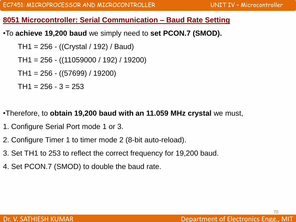
•To achieve 19,200 baud we simply need to set PCON.7 (SMOD).
TH1 = 256 - ((Crystal / 192) / Baud)
TH1 = 256 - ((11059000 / 192) / 19200)
TH1 = 256 - ((57699) / 19200)
TH1 = 256 - 3 = 253
•Therefore, to obtain 19,200 baud with an 11.059 MHz crystal we must,
1. Configure Serial Port mode 1 or 3.
2. Configure Timer 1 to timer mode 2 (8-bit auto-reload).
3. Set TH1 to 253 to reflect the correct frequency for 19,200 baud.
4. Set PCON.7 (SMOD) to double the baud rate.
EC7451: MICROPROCESSOR AND MICROCONTROLLER UNIT IV – Microcontroller
Dr. V. SATHIESH KUMAR Department of Electronics Engg., MIT71
8051 Microcontroller: Serial Communication – Writing to Serial Port
•To write a byte to the serial port one must simply write the value to the SBUF (99H)
SFR.
•For example, if you wanted to send the letter "A" to the serial port, it could be
accomplished as easily as MOV SBUF, #A
•Obviously transmission is not instantaneous, it takes a measureable amount of time
to transmit. And since the 8051 does not have a serial output buffer we need to be
sure that a character is completely transmitted before we try to transmit the next
character.
•The 8051 lets us know when it is done transmitting a character by setting the TI bit
in SCON.
•Consider the following code segment,
CLR TI ; Be sure the bit is initially clear
MOV SBUF, #A ; Send the letter A to the serial port
JNB TI,$ ; Pause until the TI bit is set.
EC7451: MICROPROCESSOR AND MICROCONTROLLER UNIT IV – Microcontroller
Dr. V. SATHIESH KUMAR Department of Electronics Engg., MIT72
8051 Microcontroller: Serial Communication – Reading from Serial Port
•To read a byte from the serial port one just needs to read the value stored in
the SBUF (99H) SFR after the 8051 has automatically set the RI flag in SCON.
•For example, if your program wants to wait for a character to be received and
subsequently read it into the Accumulator, the following code segment may be used,
JNB RI,$ ; Wait for the 8051 to set the RI flag
MOV A,SBUF ; Read the character from the serial port
•So as long as the bit is not set the program repeats the "JNB" instruction continuously.
•Once the RI bit is set upon character reception the above condition automatically fails
and program flow falls through to the "MOV" instruction which reads the value.
EC7451: MICROPROCESSOR AND MICROCONTROLLER UNIT IV – Microcontroller
Dr. V. SATHIESH KUMAR Department of Electronics Engg., MIT73
8051 Microcontroller: Addressing Modes
•In 8051 there are 1-byte, 2-byte instructions and very few 3-byte instructions.
•The opcodes are 8-bit long.
•As the opcodes are 8-bit data, there are 256 possibilities.
•Among 256, 255 opcodes are implemented.
•If the clock frequency is 12 MHz, so 64 instruction types are executed in just 1 µs,
and rest are in 2 µs.
•The Multiplication and Division operations take 4 µs to execute.
•There are six types of addressing modes:
1. Immediate Addressing Mode
2. Register Addressing Mode
3. Direct Addressing Mode
4. Register Indirect Addressing Mode
5. Indexed Addressing Mode
6. Implied Addressing Mode
EC7451: MICROPROCESSOR AND MICROCONTROLLER UNIT IV – Microcontroller
Dr. V. SATHIESH KUMAR Department of Electronics Engg., MIT74
8051 Microcontroller: Addressing Modes - Immediate
•In Immediate Addressing Mode, the data is provided in the instruction itself.
•The data is provided immediately after the opcode.
•These are some examples of Immediate Addressing Mode:
MOV A, #0AFH;
MOV R3, #45H;
MOV DPTR, #FE00H;
•In these instructions, the # symbol is used for immediate data.
•In the first instruction, the immediate data is AFH, but one 0 is added at the beginning.
•So when the data is starting with A to F, the data should be preceded by 0.
EC7451: MICROPROCESSOR AND MICROCONTROLLER UNIT IV – Microcontroller
Dr. V. SATHIESH KUMAR Department of Electronics Engg., MIT75
8051 Microcontroller: Addressing Modes - Register
•In register addressing mode, the source or destination data should be present in a
register (R0 to R7).
•These are some examples of Register Addressing Mode:
MOV A, R5;
MOV R0, A;
•n 8051, there is no instruction like MOVR5, R7.
•But we can get the same result by using this instruction MOV R5, 07H, or by
using MOV 05H, R7.
•But this two instruction will work when the selected register bank is RB0.
EC7451: MICROPROCESSOR AND MICROCONTROLLER UNIT IV – Microcontroller

Dr. V. SATHIESH KUMAR Department of Electronics Engg., MIT76
8051 Microcontroller: Addressing Modes - Direct
•In Direct Addressing Mode, the source or destination address is specified by using
8-bit address in the instruction.
•Only the internal data memory can be used in this mode.
•Here some of the examples of direct Addressing Mode:
MOV 80H, R6;
MOV R2, 45H;
MOV R0, 05H;
• The first instruction will send the content of register R6 to port P0 (Address of Port 0
is 80H).
•The second one is for getting content from 45H to R2.
•The third one is used to get data from Register R5 (When register bank RB0 is
selected) to register R0.
EC7451: MICROPROCESSOR AND MICROCONTROLLER UNIT IV – Microcontroller
Dr. V. SATHIESH KUMAR Department of Electronics Engg., MIT77
8051 Microcontroller: Addressing Modes – Register Indirect
•In this mode, the source or destination address is given in the register.
•By using register indirect addressing mode, the internal or external addresses can be
accessed.
•The R0 and R1 are used for 8-bit addresses, and DPTR is used for 16-bit
addresses, no other registers can be used for addressing purposes.
•Let us see some examples of this mode:
MOV 0E5H, @R0;
MOV @R1, 80H
• In the instructions, the @ symbol is used for register indirect addressing.
•In the first instruction, if the content of R0 is 40H, then the instruction will take the
data from location 40H of the internal RAM.
•In the second one, if the content of R1 is 30H, then it indicates that the content of
port P0 will be stored at location 30H in the internal RAM.
EC7451: MICROPROCESSOR AND MICROCONTROLLER UNIT IV – Microcontroller
Dr. V. SATHIESH KUMAR Department of Electronics Engg., MIT78
8051 Microcontroller: Addressing Modes – Register Indirect
MOVX A, @R1;
MOVX @DPTR, A;
•In these two instructions, the X in MOVX indicates the external data memory.
•The external data memory can only be accessed in register indirect mode.
•In the first instruction, if the R1 is holding 40H, then A will get the content of external
RAM location 40H.
•And in the second one, the content of A is overwritten in the location pointed by
DPTR.
EC7451: MICROPROCESSOR AND MICROCONTROLLER UNIT IV – Microcontroller
Dr. V. SATHIESH KUMAR Department of Electronics Engg., MIT79
8051 Microcontroller: Addressing Modes – Indexed
•In the indexed addressing mode, the source memory can only be accessed from
program memory.
•The destination operand is always the register A.
•These are some examples of Indexed addressing mode:
MOVC A, @A+PC;
MOVC A, @A+DPTR;
•The C in MOVC instruction refers to code byte.
•For the first instruction, let us consider A holds 30H. The PC value is 1125H.
•The contents of program memory location 1155H (30H + 1125H) are moved to
register A.
EC7451: MICROPROCESSOR AND MICROCONTROLLER UNIT IV – Microcontroller
Dr. V. SATHIESH KUMAR Department of Electronics Engg., MIT80
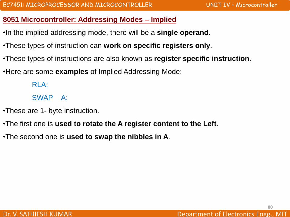
8051 Microcontroller: Addressing Modes – Implied
•In the implied addressing mode, there will be a single operand.
•These types of instruction can work on specific registers only.
•These types of instructions are also known as register specific instruction.
•Here are some examples of Implied Addressing Mode:
RLA;
SWAP A;
•These are 1- byte instruction.
•The first one is used to rotate the A register content to the Left.
•The second one is used to swap the nibbles in A.
EC7451: MICROPROCESSOR AND MICROCONTROLLER UNIT IV – Microcontroller

Dr. V. SATHIESH KUMAR Department of Electronics Engg., MIT81
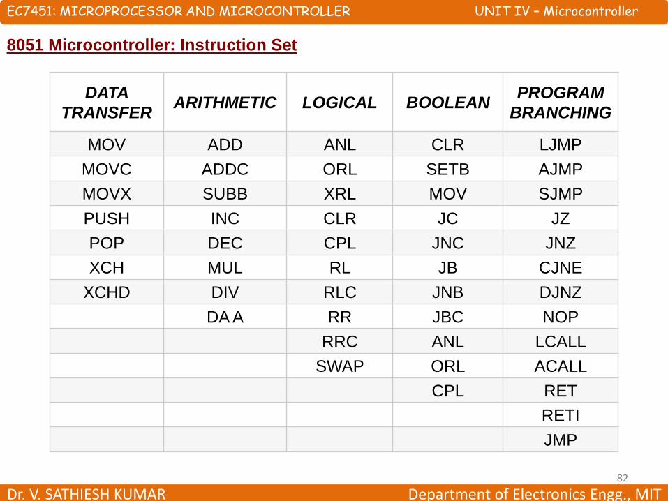
8051 Microcontroller: Instruction Set
•Based on the operation they perform, all the instructions in the 8051 Microcontroller
Instruction Set are divided into five groups. They are:
1. Data Transfer Instructions
2. Arithmetic Instructions
3. Logical Instructions
4. Boolean or Bit Manipulation Instructions
5. Program Branching Instructions
EC7451: MICROPROCESSOR AND MICROCONTROLLER UNIT IV – Microcontroller
Dr. V. SATHIESH KUMAR Department of Electronics Engg., MIT82
8051 Microcontroller: Instruction Set
EC7451: MICROPROCESSOR AND MICROCONTROLLER UNIT IV – Microcontroller
DATA
TRANSFERARITHMETIC LOGICAL BOOLEAN
PROGRAM
BRANCHING
MOV ADD ANL CLR LJMP
MOVC ADDC ORL SETB AJMP
MOVX SUBB XRL MOV SJMP
PUSH INC CLR JC JZ
POP DEC CPL JNC JNZ
XCH MUL RL JB CJNE
XCHD DIV RLC JNB DJNZ
DA A RR JBC NOP
RRC ANL LCALL
SWAP ORL ACALL
CPL RET
RETI
JMP

Dr. V. SATHIESH KUMAR Department of Electronics Engg., MIT83
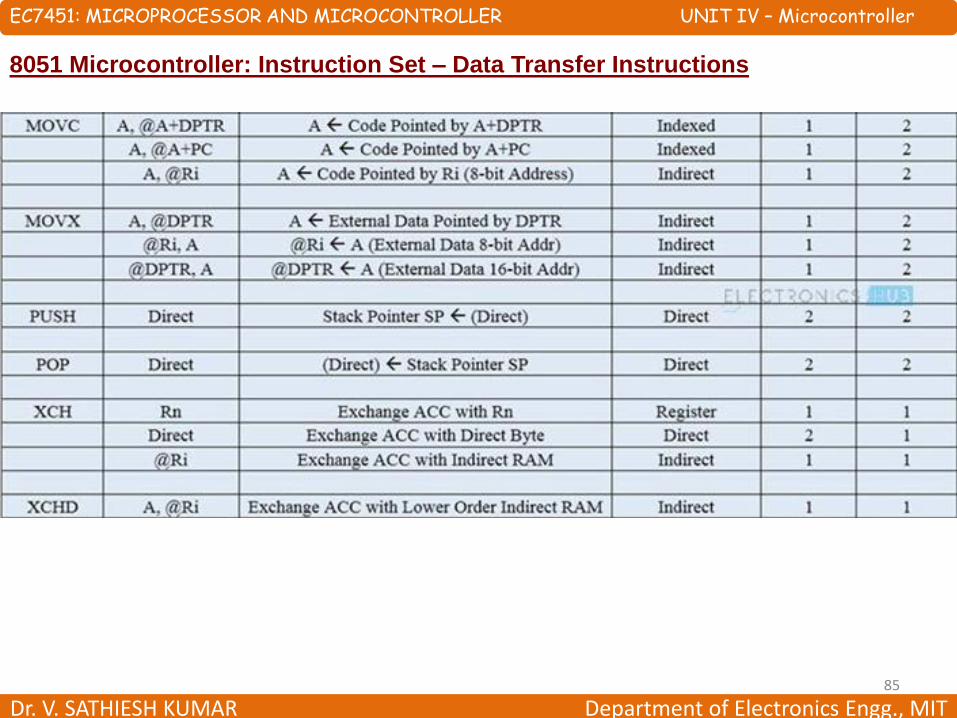
8051 Microcontroller: Instruction Set – Data Transfer Instructions
•The Data Transfer Instructions are associated with transfer of data between registers
or external program memory or external data memory.
•The mnemonics associated with Data Transfer are given below,
MOV
MOVC
MOVX
PUSH
POP
XCH
XCHD
EC7451: MICROPROCESSOR AND MICROCONTROLLER UNIT IV – Microcontroller
Dr. V. SATHIESH KUMAR Department of Electronics Engg., MIT84
8051 Microcontroller: Instruction Set – Data Transfer Instructions
EC7451: MICROPROCESSOR AND MICROCONTROLLER UNIT IV – Microcontroller
Ri – R0 or R1
Rn – R0 to R7
Dr. V. SATHIESH KUMAR Department of Electronics Engg., MIT85
8051 Microcontroller: Instruction Set – Data Transfer Instructions
EC7451: MICROPROCESSOR AND MICROCONTROLLER UNIT IV – Microcontroller
Dr. V. SATHIESH KUMAR Department of Electronics Engg., MIT86
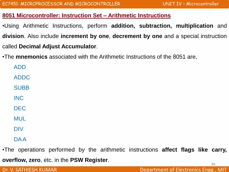
8051 Microcontroller: Instruction Set – Arithmetic Instructions
•Using Arithmetic Instructions, perform addition, subtraction, multiplication and
division. Also include increment by one, decrement by one and a special instruction
called Decimal Adjust Accumulator.
•The mnemonics associated with the Arithmetic Instructions of the 8051 are,
ADD
ADDC
SUBB
INC
DEC
MUL
DIV
DA A
•The operations performed by the arithmetic instructions affect flags like carry,
overflow, zero, etc. in the PSW Register.
EC7451: MICROPROCESSOR AND MICROCONTROLLER UNIT IV – Microcontroller
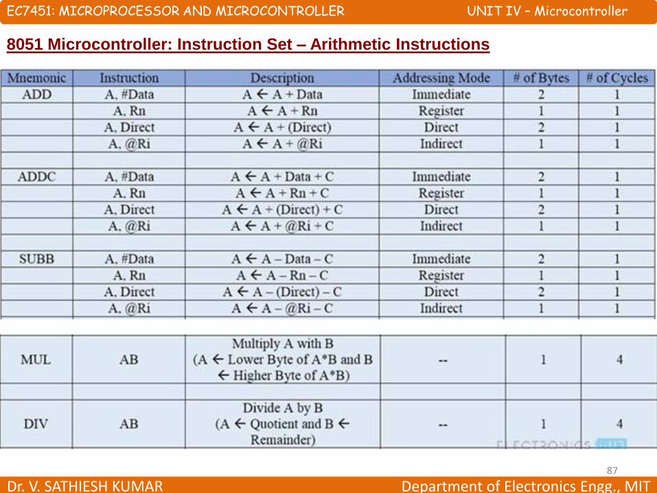
Dr. V. SATHIESH KUMAR Department of Electronics Engg., MIT87
8051 Microcontroller: Instruction Set – Arithmetic Instructions
EC7451: MICROPROCESSOR AND MICROCONTROLLER UNIT IV – Microcontroller
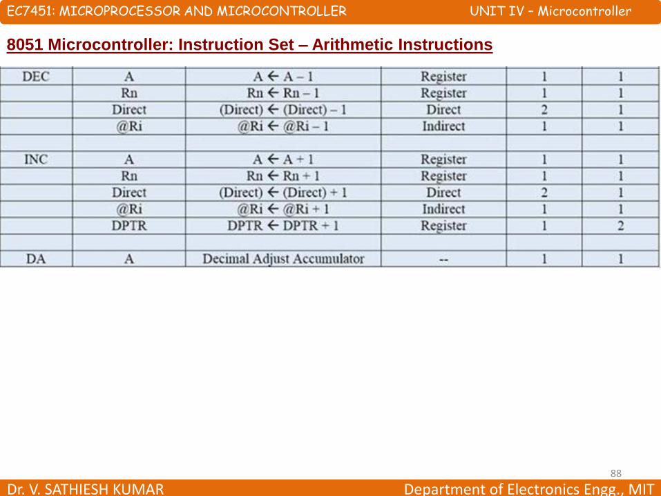
Dr. V. SATHIESH KUMAR Department of Electronics Engg., MIT88
8051 Microcontroller: Instruction Set – Arithmetic Instructions
EC7451: MICROPROCESSOR AND MICROCONTROLLER UNIT IV – Microcontroller

Dr. V. SATHIESH KUMAR Department of Electronics Engg., MIT89
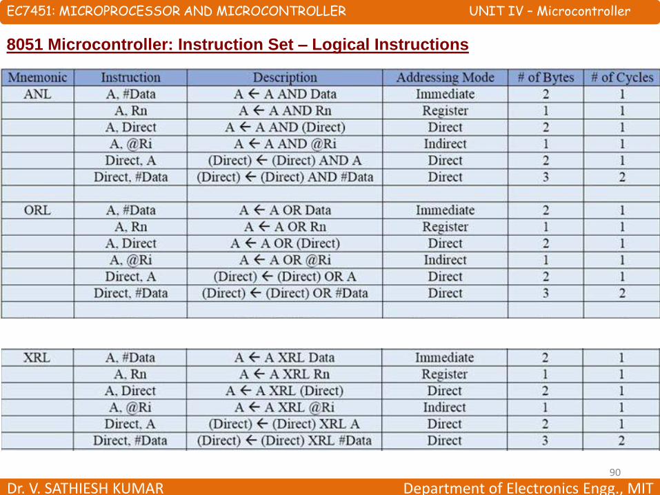
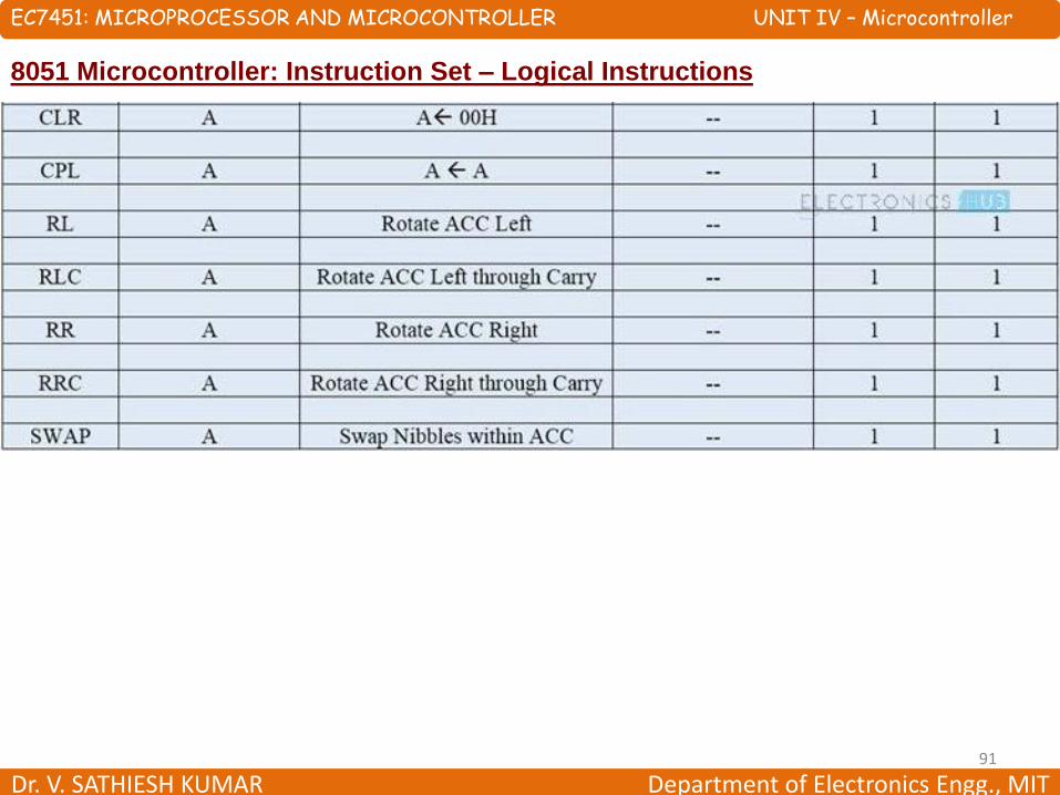
8051 Microcontroller: Instruction Set – Logical Instructions
•The Logical Instructions, perform logical operations like AND, OR, XOR, NOT, Rotate,
Clear and Swap.
•Logical operations are performed on Bytes of data on a bit-by-bit basis.
•Mnemonics associated with Logical Instructions are as follows,
ANL
ORL
XRL
CLR
CPL
RL
RLC
RR
RRC
SWAP
EC7451: MICROPROCESSOR AND MICROCONTROLLER UNIT IV – Microcontroller
Dr. V. SATHIESH KUMAR Department of Electronics Engg., MIT90
8051 Microcontroller: Instruction Set – Logical Instructions
EC7451: MICROPROCESSOR AND MICROCONTROLLER UNIT IV – Microcontroller
Dr. V. SATHIESH KUMAR Department of Electronics Engg., MIT91
8051 Microcontroller: Instruction Set – Logical Instructions
EC7451: MICROPROCESSOR AND MICROCONTROLLER UNIT IV – Microcontroller

Dr. V. SATHIESH KUMAR Department of Electronics Engg., MIT92
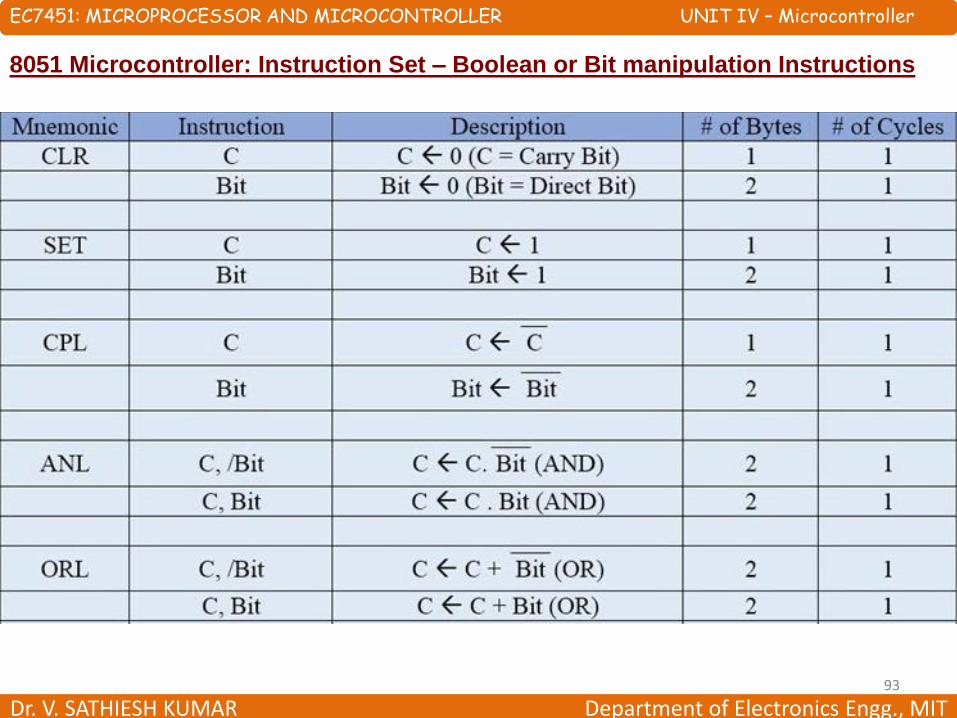
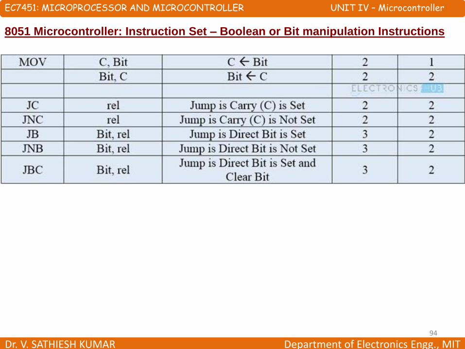
8051 Microcontroller: Instruction Set – Boolean or Bit manipulation Instructions
•Boolean or Bit Manipulation Instructions deal with bit variables.
•We know that, there is a special bit-addressable area in the RAM and some of the
Special Function Registers (SFRs) are also bit addressable.
•The Mnemonics corresponding to the Boolean or Bit Manipulation instructions are,
CLR SETB
MOV JC
JNC JB
JNB JBC
ANL ORL
CPL
EC7451: MICROPROCESSOR AND MICROCONTROLLER UNIT IV – Microcontroller
Dr. V. SATHIESH KUMAR Department of Electronics Engg., MIT93
8051 Microcontroller: Instruction Set – Boolean or Bit manipulation Instructions
EC7451: MICROPROCESSOR AND MICROCONTROLLER UNIT IV – Microcontroller
Dr. V. SATHIESH KUMAR Department of Electronics Engg., MIT94
8051 Microcontroller: Instruction Set – Boolean or Bit manipulation Instructions
EC7451: MICROPROCESSOR AND MICROCONTROLLER UNIT IV – Microcontroller

Dr. V. SATHIESH KUMAR Department of Electronics Engg., MIT95
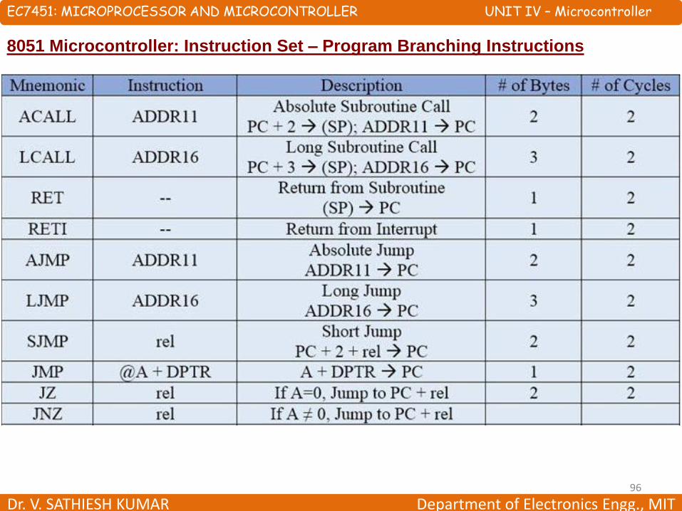
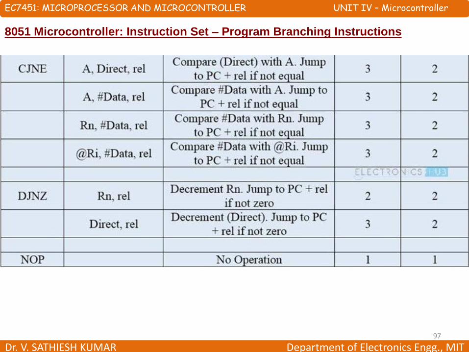
8051 Microcontroller: Instruction Set – Program Branching Instructions
•These instructions control the flow of program logic.
•The mnemonics of the Program Branching Instructions are as follows,
LJMP AJMP
SJMP JZ
JNZ CJNE
DJNZ NOP
LCALL ACALL
RET RETI
JMP
•All these instructions, except the NOP (No Operation) affect the Program Counter
(PC) in one way or other.
•Some of these instructions has decision making capability before transferring
control to other part of the program.
EC7451: MICROPROCESSOR AND MICROCONTROLLER UNIT IV – Microcontroller
Dr. V. SATHIESH KUMAR Department of Electronics Engg., MIT96
8051 Microcontroller: Instruction Set – Program Branching Instructions
EC7451: MICROPROCESSOR AND MICROCONTROLLER UNIT IV – Microcontroller
Dr. V. SATHIESH KUMAR Department of Electronics Engg., MIT97
8051 Microcontroller: Instruction Set – Program Branching Instructions
EC7451: MICROPROCESSOR AND MICROCONTROLLER UNIT IV – Microcontroller
Dr. V. SATHIESH KUMAR Department of Electronics Engg., MIT98
Summary
1. 8051 – Architecture
2. Pin details
3. Special Function Registers (SFRs)
4. I/O Ports,
5. Timers / counters
6. Interrupts and serial communication
7. Instruction set
8. Addressing modes
EC7451: MICROPROCESSOR AND MICROCONTROLLER UNIT IV – Microcontroller