ec2205 – electronic circuits-1 unit iii frequency ... emitter amplifier is most popular bjt...
TRANSCRIPT

EC2205 – Electronic Circuits-1
UNIT III
FREQUENCY RESPONSE OF AMPLIFIERS
PART –A (2 MARK QUESTIONS)
1. Two amplifiers having gain 20 dB and 40 dB are cascaded. Find the overall gain in
dB. (NOV/DEC 2009)
The over all gain of the cascade amplifier = A1* A2 = 60 DB
2. Define Bandwidth(NOV/DEC 2009)
Band Width = f2 – f1 , where f2 and f1 are upper and lower cut-off frequencies.
3. Give the expressions for gain bandwidth product. (APR/MAY 2010)
It is a frequency at which the short circuit common Emitter current gain has a magnitude
of unity.FT = hfe fβ, where hfe – low frequency current gain and fβ- Cut-off frequency.
4. What do you mean by amplifier rise time? (APR/MAY 2010)
It is time required for a wave form to change from 10% of its final value to 90% of its final
value.
5. Why common base amplifier is preferred for high frequency signal when
compared to common emitter amplifier? (NOV/DEC 2010)
6. Mention the effect of coupling capacitors on the bandwidth of the amplifier.
(NOV/DEC 2011)
In the mid frequency range, reactance of CC is negligible.
The lower 3-dB frequency fl = 1/[2π(Rs +Ri’)CC], for good low frequency response CC
should be large.
7. Draw the general shape of the Frequency response of amplifiers.

8. Draw the hybrid π equivalent circuit of BJTs.
9. Define base spreading resistance (rbb’).
It is the internal resistance between the base terminal and virtual base terminal of the
bipolar junction transistor.
10. Give the relationship between rise time and bandwidth.
Tr = 0.35/BW seconds
Tr – rise time
BW- Band width
11. What is the difference between single stage and multistage amplifiers?
1. The overall amplification is higher.
2. Less non-linear distortion
3. Frequency response is much better.

12. The midband gain of an amplifier is 100 and the lower cutoff frequency is 1khz.
Find the gain of the amplifier at a frequency of 20 Hz.
AV = -20 log10(20/103)
13. If rise time of BJT is 3.5 micro sec, find out its transition frequency.
Tr = 0.35/BW secs
3.5x 10-6 = .35/BW
BW = .35/3.5x 10-6 HZ
14. Define Gain Bandwidth product. (NOV/DEC’12)
FT = hfe fβ, where hfe – low frequency current gain and fβ- Cut-off frequency.
15. Draw the high frequency equivalent circuit of FETs. (NOV/DEC’12)
PART- B (16 MARK QUESTIONS)
1. Discuss the frequency response of multistage amplifiers. Calculate the overall
upper and lower cutoff frequencies. (10) (NOV/DEC 2009) (NOV/DEC’12) (ii)
Discuss the terms rise time and sag. (6) (NOV/DEC 2009)
Multistage Amplifier:
Characteristic
Common
Common CommonEmitter Collector
Input impedance Low
Medium High
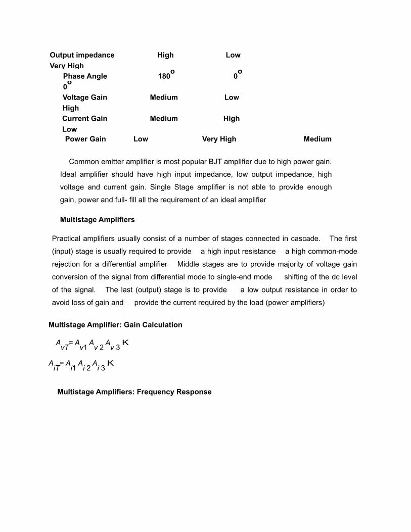
Output impedance
Very High
High Low
Phase Angle
0o
180o
0o
Voltage Gain
High
Medium Low
Current Gain
Low
Medium High
Power Gain Low Very High Medium
Common emitter amplifier is most popular BJT amplifier due to high power gain.
Ideal amplifier should have high input impedance, low output impedance, high
voltage and current gain. Single Stage amplifier is not able to provide enough
gain, power and full- fill all the requirement of an ideal amplifier
Multistage Amplifiers
Practical amplifiers usually consist of a number of stages connected in cascade. The first
(input) stage is usually required to provide a high input resistance a high common-mode
rejection for a differential amplifier Middle stages are to provide majority of voltage gain
conversion of the signal from differential mode to single-end mode shifting of the dc level
of the signal. The last (output) stage is to provide a low output resistance in order to
avoid loss of gain and provide the current required by the load (power amplifiers)
Multistage Amplifier: Gain Calculation
AvT
= Av1
Av 2
Av 3
K
A
iT= A
i1 A
i 2 A
i 3 K
Multistage Amplifiers: Frequency Response

High cut off frequency
Where n is the number of cascaded stage


2. Discuss the high frequency equivalent circuit of FET and hence derive gain
bandwidth product for any one configuration. (NOV/DEC 2009).
High frequency response of CS amplifier
The JFET implementation of the common-source amplifier is given to the leftbelow, and
the small signal circuit incorporating thehigh frequency FET model is given to the right
below.As stated above, the external coupling and bypass capacitors arelarge enough
that we can model them as short circuits for high frequencies.We may simplifythe small
signal circuit by making the following approximations and observations:

¾ rdsis usually larger than RD||RL, so that the parallel combination is dominated by
RD||RLandrds may be neglected. If this is not the case, asingle equivalent resistance,
rds||RD||RLmay be defined.¾ TheMillereffect transforms Cgdinto separate capacitances
seen in the input and output circuits as
The parallel capacitances in the input circuit, Cgsand CM1, may becombined to a single
equivalent capacitance of value
Similarly, the parallel capacitances in the output circuit, Cdsand CM2, may be combined
to a single equivalent capacitance of value
With theabove simplifications, the small signal circuit may be
Cin:SettingCpitand CS equalto zero (open circuit),the equivalentresistanceseen by
Cinis
Cout:Letting the impedance of Cin be equalto infinity, the equivalent
resistanceseen by Coutis

The highfrequency time constants for the CS amplifier are therefore defined
the upper corner frequency is approximated by
Highequency cutoff is given byGenerally,
3. Discuss the low frequency response and the high frequency response of
an amplifier. (16) (APR/MAY 2010)

4. Explain the operation of high frequency common source FET amplifier
with neat diagram. Derive the expression for (i) voltage gain (ii) input
admittance (iii) input capacitance (iv) output admittance. (16) (APR/MAY 2010)

5. Draw the Hybrid π? equivalent circuit of a BJT. (4) (ii) Using hybrid ? model, draw
the high frequency equivalent circuit of CE amplifier and derive for higher cut-off
frequencies. (12) (NOV/DEC 2010)
Common Emitter Amplifier
DC analysis: Recall that an emitter resistor is necessary to provide stability of the bias point. As such, the circuit conguration as is shown has as a poor bias. We need to include RE for good biasing (DC signals) and eliminate it for AC signals.The solution to include an emitter resistance and use a \bypass" capacitor to shortit out for AC signals as is shown.
AC analysis: To start the analysis, we kill all DC sources, combine R1 and R2 into RB and replace the BJT with its small signal model. We see that emitter is now common between input and output AC signals (thus, common emitter amplifier. Analysis of this circuit is straightforward. Examination of the circuit shows that:


6. Explain in detail with neat diagram frequency response of BJT amplifier. Discuss
the significance of cut off frequencies and Bandwidth of the amplifier. (16)
(NOV/DEC 2011)

7. Derive the expression for frequency response of multistage amplifier. (10)(ii)
discuss the significance of cut off frequencies and Gain bandwidth product of
amplifier. (6) (NOV/DEC 2011) (NOV/DEC’12)
The gain–bandwidth product (designated as GBWP, GBW, GBP or GB) for an amplifier is
the product of the amplifier'sbandwidth and the gain at which the bandwidth is measured.


8. Define fα,fβ and fT and state the relation between fβ and fT
Alpha cutoff frequency, falpha is the frequency at which the α falls to 0.707 of
low frequency α,0 α=0.707α0. Alpha cutoff and beta cutoff are nearly equal:
falpha fT≅ Beta cutoff fT is the preferred figure of merit of high frequency performance.
fmax is the highest frequency of oscillation possible under the most favorable conditions
of bias and impedance matching. It is the frequency at which the power gain is unity. All
of the output is fed back to the input to sustain oscillations. fmax is an upper
limit for frequency of operation of a transistor as an active device. Though, a practical
amplifier would not be usable at fmax.
Beta cutoff frequency fβ is the frequency at which ω = ωβ i.e. the magnitude of the
common-emitter current gain decreases by a factor of √2

Common emitter cutoff frequency fΤ is the frequency at which the magnitude of the
common emitter current gain equals unity, that is, |βω| = 1.
9. Define unity gain frequency. Obtain the necessary relation using transistor
frequency response.
It is a frequency at which the short circuit current gain f the CE amplifier is unity.
The gain ratio for CE amplifier is
Ai = hfe /
At f=fT |Ai| = 1
(fT/ fβ )2 >>1
1= hfe/ (fT/ fβ )
(fT/ fβ )= hfe
fT = hfe fβ
A(f) = 1 = gm/ 2πCcf
Fu = gm/ 2πCc
Ai = - hfe/ 1+j hfe(f/fT)

10. Discuss the frequency response characteristics of RC coupled amplifier.
(NOV/DEC’12)
frequency response curve of a RC coupled amplifier.
The curve is usually plotted on a semilog graph paper with frequency range on logarithmic scale so that large frequency range can be accommodated. The gain is constant for a limited band of frequencies. This range is called mid-frequency band and gain is called mid band gain. AVM. On both sides of the mid frequency range, the gain decreases. For very low and very high frequencies the gain is almost zero.In mid band frequency range, the coupling capacitors and bypass capacitors are as good as short circuits. But when the frequency is low. These capacitors can no longer be replaced by the short circuit approximation.
First consider coupling capacitor. The ac equivalent is shown in fig. 3, assuming capacitors are offering some impedance. In mid-frequency band, the capacitors are ac shorted so the input voltage appears directly across br'e but at low frequency the XC is significant and some voltage drops across XC. The input vin at the base decreases. Thus decreasing output voltage. The lower the frequency the more will be XC and lesser will be the output voltage.
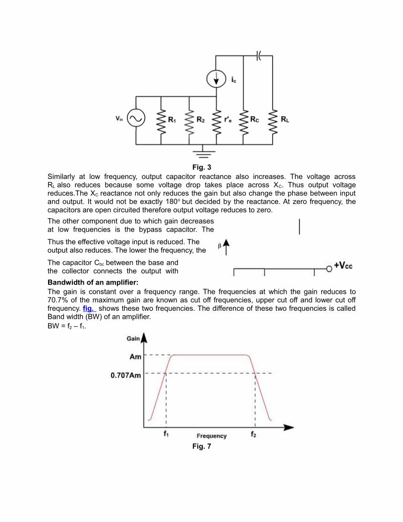
Fig. 3Similarly at low frequency, output capacitor reactance also increases. The voltage across RL also reduces because some voltage drop takes place across XC. Thus output voltage reduces.The XC reactance not only reduces the gain but also change the phase between input and output. It would not be exactly 180o but decided by the reactance. At zero frequency, the capacitors are open circuited therefore output voltage reduces to zero.
The other component due to which gain decreases at low frequencies is the bypass capacitor. The function of this capacitor is to bypass ac and blocks Thus the effective voltage input is reduced. The output also reduces. The lower the frequency, the lesser will be the gain. This reduction in gain is due
The capacitor Cbc between the base and the collector connects the output with the input. Because of this, negative Bandwidth of an amplifier:The gain is constant over a frequency range. The frequencies at which the gain reduces to 70.7% of the maximum gain are known as cut off frequencies, upper cut off and lower cut off frequency. fig. shows these two frequencies. The difference of these two frequencies is called Band width (BW) of an amplifier.BW = f2 – f1.
Fig. 7

At f1 and f2, the voltage gain becomes 0.707 Am(1 / Ö 2). The output voltage reduces to 1 / Ö 2 of maximum output voltage. Since the power is proportional to voltage square, the output power at these frequencies becomes half of maximum power. The gain on dB scale is given by20 log10(V2 / V1) = 10 log 10 (V2 / V1)2 = 3 dB.20 log10(V2 / V1) = 20 log10(0.707) =10 log10 (1 / Ö 2)2 = 10 log10(1 / 2) = -3 dB.If the difference in gain is more than 3 dB, then it can be detected by human. If it is less than 3 dB it cannot be detected.