e mmc 5.1 hs400) - delson technology · introduction e •mmc™ 4.5 ... capacity boot partition 1...
TRANSCRIPT
____________________________________________________________________________________________________________________
1
Flash Storage Specification e•MMC™ 5.1
Flash Storage Specification
e•MMC™ 4.5
Flash Storage Specification
e•MMC™ 4.5
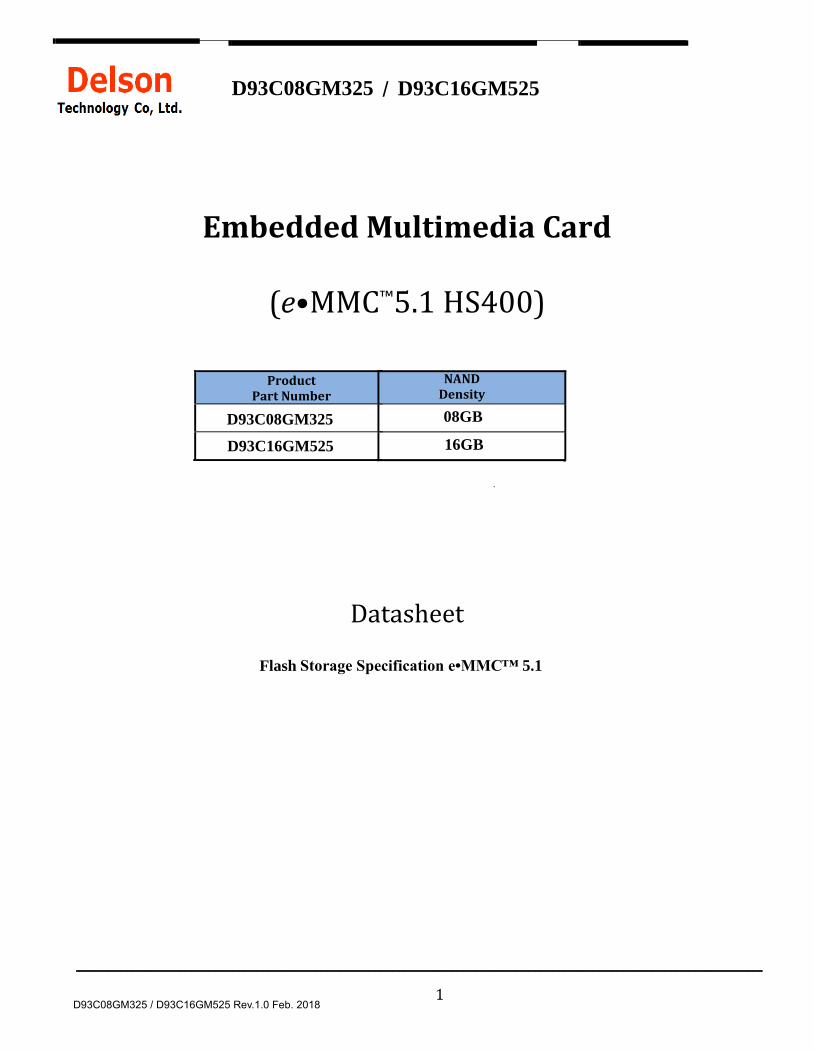
Embedded Multimedia Card
(e•MMC™5.1 HS400)
Datasheet
D93C08GM325 / D93C16GM525 Rev.1.0 Feb. 2018
D93C08GM325
Product Part Number
D93C16GM525
NAND Density
16GB
08GB
D93C08GM325 D93C16GM525 /
____________________________________________________________________________________________________________________
2
e• ™ 4.5
Flash Storage Specification
e•MMC™ 4.5 CONTENTS
Product Features: ..................................................................................................................................................4
1. Introduction ........................................................................................................................................................5 2. Specification .......................................................................................................................................................5
2.1. System Performance ....................................................................................................................................5 2.2. Power Consumption .....................................................................................................................................5 2.3. Capacity according to partition ................................................................................................................6 2.4. User Density ....................................................................................................................................................6
3. e•MMC™ Device and System ...........................................................................................................................7 3.1. e•MMC™ System Overview ..........................................................................................................................7 3.2. Memory Addressing .....................................................................................................................................7 3.3. e•MMC™ Device Overview ...........................................................................................................................8
3.3.1 Clock (CLK) ..............................................................................................................................................8 3.3.2 Data Strobe(DS).....................................................................................................................................8 3.3.3 Command (CMD) ...................................................................................................................................8 3.3.4 Input/Outputs (DAT0-DAT7) ...........................................................................................................8
3.4. Bus Protocol ....................................................................................................................................................9 3.5. Bus Speed Modes ...........................................................................................................................................9
3.5.1 HS200 Bus Speed Mode ................................................................................................................... 10 3.5.2 HS200 System Block Diagram ....................................................................................................... 10 3.5.3 HS400 Bus Speed mode ................................................................................................................... 10 3.5.4 HS400 System Block Diagram ....................................................................................................... 11
4. e•MMC™ Functional Description ............................................................................................................... 12 4.1 e•MMC™ Overview....................................................................................................................................... 12 4.2 Boot Operation Mode ................................................................................................................................ 12 4.3 Device Identification Mode ..................................................................................................................... 12 4.4 Interrupt Mode ............................................................................................................................................ 12 4.5 Data Transfer Mode ................................................................................................................................... 12 4.6 Inactive Mode .............................................................................................................................................. 13 4.7 H/W Reset Operation ................................................................................................................................ 13 4.8 Noise Filtering Timing for H/W Reset ................................................................................................. 14 4.9 Field Firmware Update(FFU) ................................................................................................................. 15 4.10 Power off Notification for sleep .......................................................................................................... 16 4.11 Cache Enhancement Barrier ................................................................................................................ 17 4.12 Cache Flushing Policy ............................................................................................................................. 19 4.13 Command Queueing ................................................................................................................................ 20
5. Register Settings ............................................................................................................................................ 21 5.1. OCR Register ................................................................................................................................................ 21 5.2. CID Register .................................................................................................................................................. 21 5.3. CSD Register ................................................................................................................................................. 21 5.4. Extended CSD Register ............................................................................................................................. 21 5.5. RCA Register ................................................................................................................................................. 21 5.6. DSR Register ................................................................................................................................................. 21
Internet
Data
Sheet
DELSON TECHNOLOGY D93C08GM325 D93C16GM525 /
____________________________________________________________________________________________________________________
3
Flash Storage Specification
e•MMC™ 4.5
Flash Storage Specification
e•MMC™ 4.5 6. The e•MMC™ bus ............................................................................................................................................. 22 6.1 Power-up ....................................................................................................................................................... 23
6.1.1 e•MMC™ power-up ............................................................................................................................. 23 6.1.2 e•MMC™ Power Cycling ..................................................................................................................... 24
6.2 Bus Operating Conditions ....................................................................................................................... 25 6.2.1 Power supply: e•MMC™ .................................................................................................................... 25 6.2.2 e•MMC™ Power Supply Voltage ..................................................................................................... 26 6.2.3 Bus Signal Line Load ......................................................................................................................... 27 6.2.4 HS400 reference load ....................................................................................................................... 28
6.3 Bus Signal Levels ........................................................................................................................................ 29 6.3.1 Open-drain Mode Bus Signal Level .............................................................................................. 29 6.3.2 Push-pull mode bus signal level— e•MMC™ .............................................................................. 29 6.3.3 Bus Operating Conditions for HS200 & HS400 ........................................................................ 30 6.3.4 Device Output Driver Requirements for HS200 & HS400 ................................................... 30
6.4 Bus Timing .................................................................................................................................................... 30 6.4.1 Device Interface Timings ................................................................................................................ 31
6.5 Bus Timing for DAT Signals During Dual Data Rate Operation.................................................. 32 6.6 Bus Timing Specification in HS200 Mode .......................................................................................... 33 6.7 Bus Timing Specification in HS400 mode .......................................................................................... 37
6.7.1 HS400 Device Input Timing ........................................................................................................... 37 6.7.2 HS400 Device Output Timing ........................................................................................................ 38
7. Package connections .................................................................................................................................... 40 8. Ball Assignment (153 ball) ......................................................................................................................... 42 9. Temperature ................................................................................................................................................... 43 10. Revision History ............................................................................................................................................. 44
Internet
Data
Sheet DELSON TECHNOLOGY D93C08GM325 D93C16GM525 /
____________________________________________________________________________________________________________________
4
e•MMC™ 4.5
Flash Storage Specification
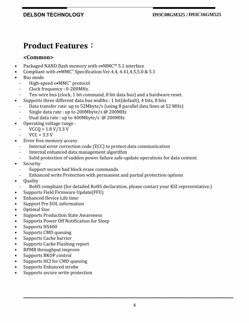
e•MMC™ 4.5 Product Features:
<Common>
• Packaged NAND flash memory with e•MMC™ 5.1 interface • Compliant with e•MMC™ Specification Ver.4.4, 4.41,4.5,5.0 & 5.1 • Bus mode
- High-speed e•MMC™ protocol - Clock frequency : 0-200MHz. - Ten-wire bus (clock, 1 bit command, 8 bit data bus) and a hardware reset.
• Supports three different data bus widths : 1 bit(default), 4 bits, 8 bits - Data transfer rate: up to 52Mbyte/s (using 8 parallel data lines at 52 MHz) - Single data rate : up to 200Mbyte/s @ 200MHz - Dual data rate : up to 400Mbyte/s @ 200MHz
• Operating voltage range : - VCCQ = 1.8 V/3.3 V - VCC = 3.3 V
• Error free memory access - Internal error correction code (ECC) to protect data communication - Internal enhanced data management algorithm - Solid protection of sudden power failure safe-update operations for data content
• Security - Support secure bad block erase commands - Enhanced write Protection with permanent and partial protection options
• Quality - RoHS compliant (for detailed RoHS declaration, please contact your KSI representative.)
• Supports Field Firmware Update(FFU) • Enhanced Device Life time • Support Pre EOL information • Optimal Size • Supports Production State Awareness • Supports Power Off Notification for Sleep • Supports HS400 • Supports CMD queuing • Supports Cache barrier • Supports Cache Flushing report • RPMB throughput improve • Supports BKOP control • Supports HCI for CMD queuing • Supports Enhanced strobe • Supports secure write protection
Internet
Data
Sheet DELSON TECHNOLOGY D93C08GM325 D93C16GM525 /
____________________________________________________________________________________________________________________
5
e•MMC™ 4.5
Flash Storage Specification
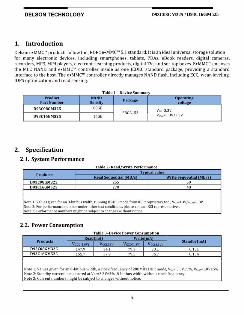
e•MMC™ 4.5 1. Introduction
Delson e•MMC™ products follow the JEDEC e•MMC™ 5.1 standard. It is an ideal universal storage solution for many electronic devices, including smartphones, tablets, PDAs, eBook readers, digital cameras, recorders, MP3, MP4 players, electronic learning products, digital TVs and set-top boxes. E•MMC™ encloses the MLC NAND and e•MMC™ controller inside as one JEDEC standard package, providing a standard interface to the host. The e•MMC™ controller directly manages NAND flash, including ECC, wear-leveling, IOPS optimization and read sensing.
Table 1 – Device Summary Product
Part Number NAND
Density Package
Operating voltage
08GB FBGA153
VCC=3.3V, VCCQ=1.8V/3.3V 16GB
2. Specification
2.1. System Performance
Table 2- Read/Write Performance
Products Typical value
Read Sequential (MB/s) Write Sequential (MB/s)
D93C08GM325 255 50
270 40
Note 1: Values given for an 8-bit bus width, running HS400 mode from KSI proprietary tool, VCC=3.3V,VCCQ=1.8V. Note 2: For performance number under other test conditions, please contact KSI representatives. Note 3: Performance numbers might be subject to changes without notice.
2.2. Power Consumption
Table 3–Device Power Consumption
Products Read(mA) Write(mA)
Standby(mA) VCCQ(1.8V) VCC(3.3V) VCCQ(1.8V) VCC(3.3V)
147.9 34.1 79.3 30.1 0.151
155.7 37.9 79.5 36.7 0.154
Note 1: Values given for an 8-bit bus width, a clock frequency of 200MHz DDR mode, VCC= 3.3V±5%, VCCQ=1.8V±5% Note 2: Standby current is measured at Vcc=3.3V±5% ,8-bit bus width without clock frequency. Note 3: Current numbers might be subject to changes without notice.
Internet
Data
Sheet DELSON TECHNOLOGY D93C08GM325 D93C16GM525 /
D93C16GM525
D93C08GM325 D93C16GM525
D93C08GM325
D93C16GM525
____________________________________________________________________________________________________________________
6
Flash Storage Specification
e•MMC™ 4.5
Flash Storage Specification
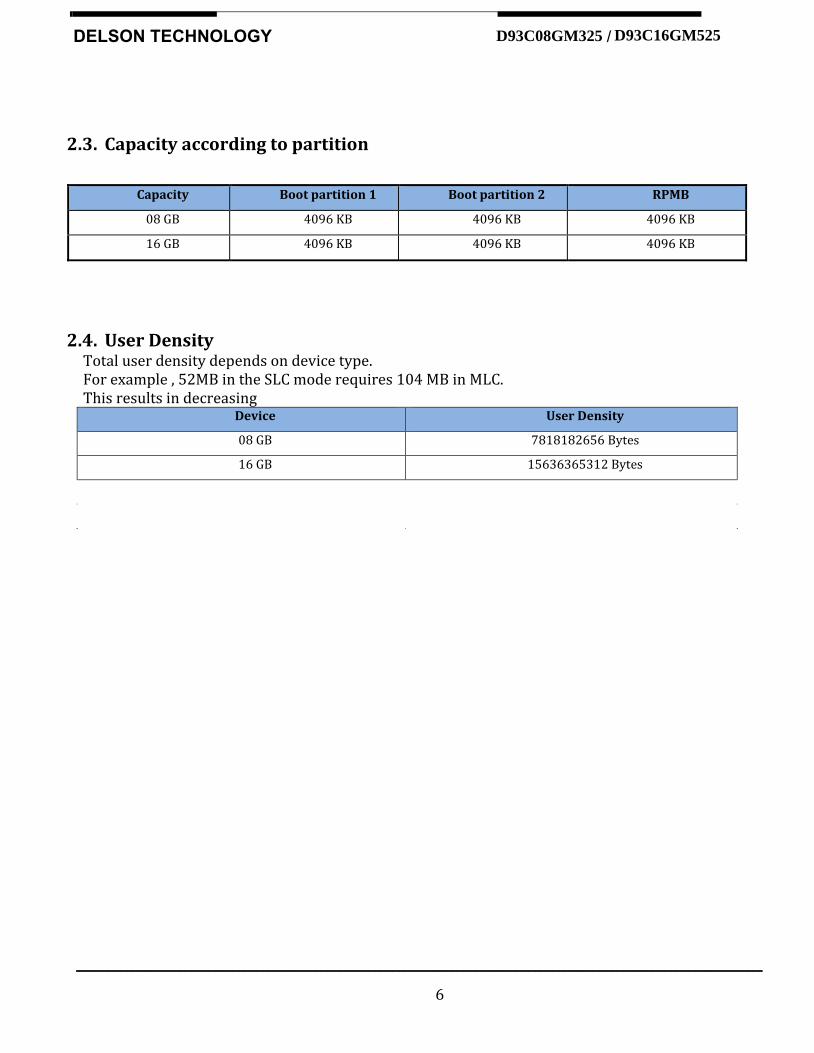
e•MMC™ 4.5 2.3. Capacity according to partition
Capacity Boot partition 1 Boot partition 2 RPMB
08 GB 4096 KB 4096 KB 4096 KB
16 GB 4096 KB 4096 KB 4096 KB
2.4. User Density Total user density depends on device type. For example , 52MB in the SLC mode requires 104 MB in MLC. This results in decreasing
Device User Density
08 GB 7818182656 Bytes
16 GB 15636365312 Bytes
Internet
Data
Sheet DELSON TECHNOLOGY D93C08GM325 D93C16GM525 /
____________________________________________________________________________________________________________________
7
e MMC™ 4.5
Flash Storage Specification
e•MMC™ 4.5 3. e•MMC™ Device and System
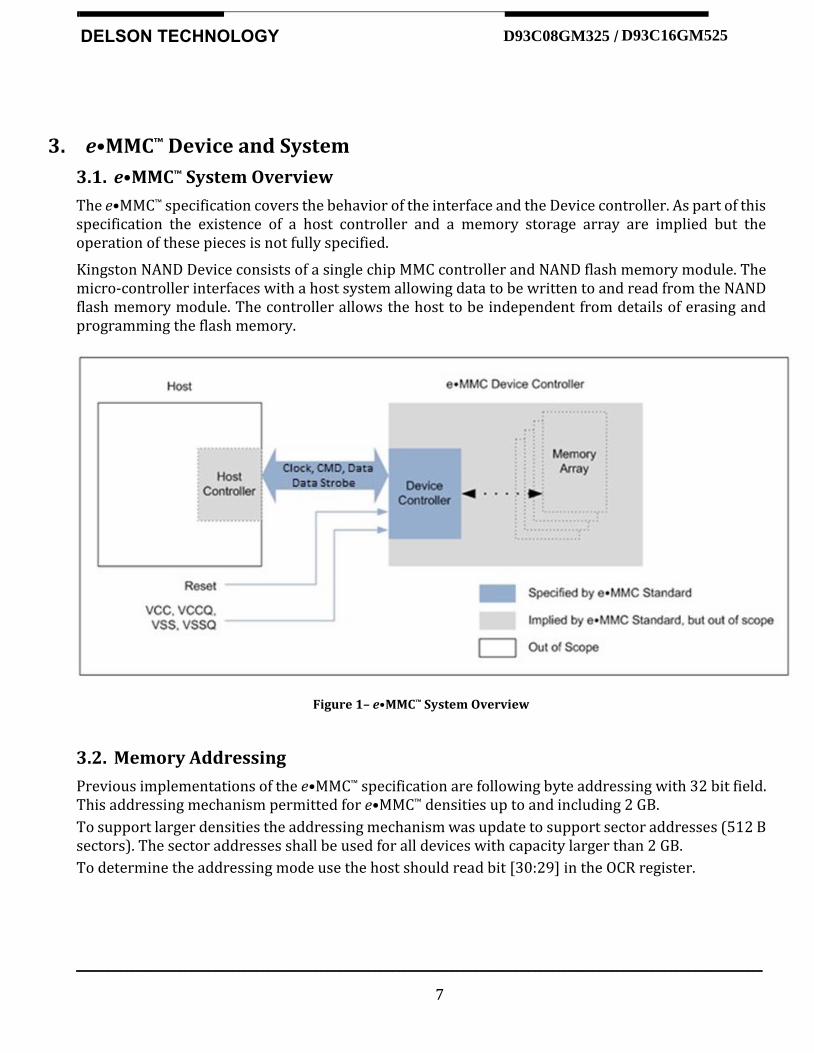
3.1. e•MMC™ System Overview
The e•MMC™ specification covers the behavior of the interface and the Device controller. As part of this specification the existence of a host controller and a memory storage array are implied but the operation of these pieces is not fully specified.
Kingston NAND Device consists of a single chip MMC controller and NAND flash memory module. The micro-controller interfaces with a host system allowing data to be written to and read from the NAND flash memory module. The controller allows the host to be independent from details of erasing and programming the flash memory.
Figure 1– e•MMC™ System Overview
3.2. Memory Addressing
Previous implementations of the e•MMC™ specification are following byte addressing with 32 bit field. This addressing mechanism permitted for e•MMC™ densities up to and including 2 GB.
To support larger densities the addressing mechanism was update to support sector addresses (512 B sectors). The sector addresses shall be used for all devices with capacity larger than 2 GB.
To determine the addressing mode use the host should read bit [30:29] in the OCR register.
Internet
Data
Sheet DELSON TECHNOLOGY D93C08GM325 D93C16GM525 /
____________________________________________________________________________________________________________________
8
e•MMC™ 4.5
Flash Storage Specification
e•MMC™ 4.5 3.3. e•MMC™ Device Overview
The e•MMC™ device transfers data via a configurable number of data bus signals. The communication signals are:
3.3.1 Clock (CLK)
Each cycle of this signal directs a one bit transfer on the command and either a one bit (1x) or a two bits transfer (2x) on all the data lines. The frequency may vary between zero and the maximum clock frequency. 3.3.2 Data Strobe(DS)
This signal is generated by the device and used for output in HS400 mode. The frequency of this signal follows the frequency of CLK. For data output each cycle of this signal directs two bits transfer(2x) on the data - one bit for positive edge and the other bit for negative edge. For CRC status response output and CMD response output(enabled only HS400 enhanced strobe mode), the CRC status is latched on the positive edge only, and don't care on the negative edge. 3.3.3 Command (CMD)
This signal is a bidirectional command channel used for Device initialization and transfer of commands. The CMD signal has two operation modes: open-drain for initialization mode, and push-pull for fast command transfer. Commands are sent from the e•MMC™ host controller to the e•MMC™ Device and responses are sent from the Device to the host. 3.3.4 Input/Outputs (DAT0-DAT7)
These are bidirectional data channels. The DAT signals operate in push-pull mode. Only the Device or the host is driving these signals at a time. By default, after power up or reset, only DAT0 is used for data transfer. A wider data bus can be configured for data transfer, using either DAT0-DAT3 or DAT0-DAT7, by the e•MMC™ host controller. The e•MMC™ Device includes internal pull-ups for data lines DAT1-DAT7. Immediately after entering the 4-bit mode, the Device disconnects the internal pull ups of lines DAT1, DAT2, and DAT3. Correspondingly, immediately after entering to the 8-bit mode the Device disconnects the internal pull-ups of lines DAT1–DAT7.
Table 4– Communication Interface
Name Type1 Description
CLK I Clock
DAT0 I/O/PP Data
DAT1 I/O/PP Data
DAT2 I/O/PP Data
DAT3 I/O/PP Data
DAT4 I/O/PP Data
DAT5 I/O/PP Data
DAT6 I/O/PP Data
DAT7 I/O/PP Data
Internet
Data
Sheet DELSON TECHNOLOGY D93C08GM325 D93C16GM525 /
____________________________________________________________________________________________________________________
9
e•MMC™ 4.5
Flash Storage Specification
e•MMC™ 4.5 CMD I/O/PP/OD Command/Response
RST_n I Hardware reset
VCC S Supply voltage for Core
VCCQ S Supply voltage for I/O
VSS S Supply voltage ground for Core
VSSQ S Supply voltage ground for I/O
DS O/PP Data strobe
Note1:I: input; O: output; PP: push-pull; OD: open-drain; NC: Not connected (or logical high); S: power supply.
Table 5– e•MMC™ Registers
Name Width
(Bytes) Description Implementation
CID 16 Device Identification number, an individual number for identification. Mandatory
RCA 2 Relative Device Address is the Device system address, dynamically assigned by the host during initialization.
Mandatory
DSR 2 Driver Stage Register, to configure the Device’s output drivers. Optional
CSD 16 Device Specific Data, information about the Device operation conditions.
Mandatory
OCR 4 Operation Conditions Register. Used by a special broadcast command to identify the voltage type of the Device.
Mandatory
EXT_CSD 512 Extended Device Specific Data. Contains information about the Device capabilities and selected modes. Introduced in standard v4.0
Mandatory
The host may reset the device by:
• Switching the power supply off and back on. The device shall have its own power-on detection circuitry which puts the device into a defined state after the power-on Device.
• A reset signal • By sending a special command
3.4. Bus Protocol
After a power-on reset, the host must initialize the device by a special message-based e•MMC™ bus protocol. For more details, refer to section 5.3.1 of the JEDEC Standard Specification No.JESD84-B51.
3.5. Bus Speed Modes
e•MMC™ defines several bus speed modes as shown in Table 6.
Table 6— Bus Speed Mode
Mode Name Data Rate IO Voltage Bus Width Frequency Max Data Transfer
(implies x8 bus width)
Backwards Compatibility with legacy MMC card
Single 3.3/1.8V 1, 4, 8 0-26MHz 26MB/s
High Speed SDR Single 3.3/1.8V 4, 8 0-52MHz 52MB/s
High Speed DDR Dual 3.3/1.8V 4, 8 0-52MHz 104MB/s
HS200 Single 1.8V 4, 8 0-200MHz 200MB/s
HS400 Dual 1.8V 8 0-200MHz 400MB/s
Internet
Data
Sheet DELSON TECHNOLOGY D93C08GM325 D93C16GM525 /
____________________________________________________________________________________________________________________
10
Flash Storage Specification
e•MMC™ 4.5 3.5.1 HS200 Bus Speed Mode
The HS200 mode offers the following features:
• SDR Data sampling method • CLK frequency up to 200MHz Data rate – up to 200MB/s • 8-bits bus width supported • Single ended signaling with 4 selectable Drive Strength • Signaling levels of 1.8V • Tuning concept for Read Operations
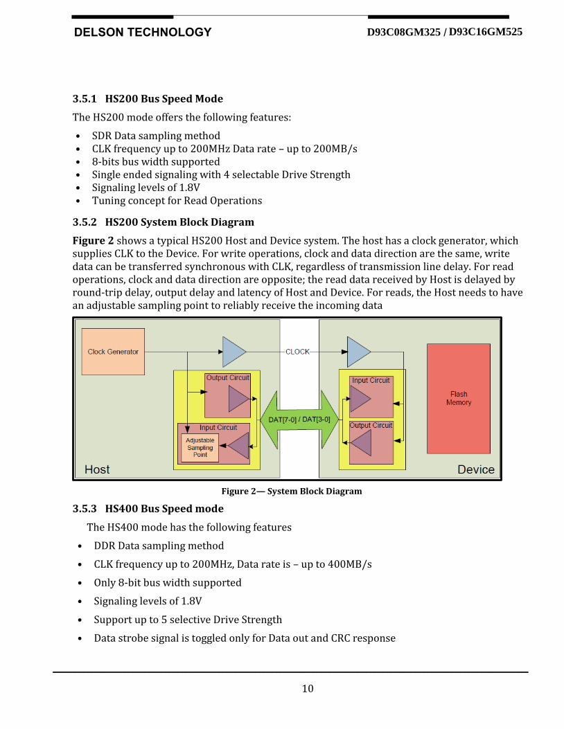
3.5.2 HS200 System Block Diagram
Figure 2 shows a typical HS200 Host and Device system. The host has a clock generator, which supplies CLK to the Device. For write operations, clock and data direction are the same, write data can be transferred synchronous with CLK, regardless of transmission line delay. For read operations, clock and data direction are opposite; the read data received by Host is delayed by round-trip delay, output delay and latency of Host and Device. For reads, the Host needs to have an adjustable sampling point to reliably receive the incoming data
Figure 2— System Block Diagram
3.5.3 HS400 Bus Speed mode
The HS400 mode has the following features
• DDR Data sampling method
• CLK frequency up to 200MHz, Data rate is – up to 400MB/s
• Only 8-bit bus width supported
• Signaling levels of 1.8V
• Support up to 5 selective Drive Strength
• Data strobe signal is toggled only for Data out and CRC response
Internet
Data
Sheet DELSON TECHNOLOGY D93C08GM325 D93C16GM525 /
____________________________________________________________________________________________________________________
11
Flash Storage Specification
e•MMC™ 4.5 3.5.4 HS400 System Block Diagram
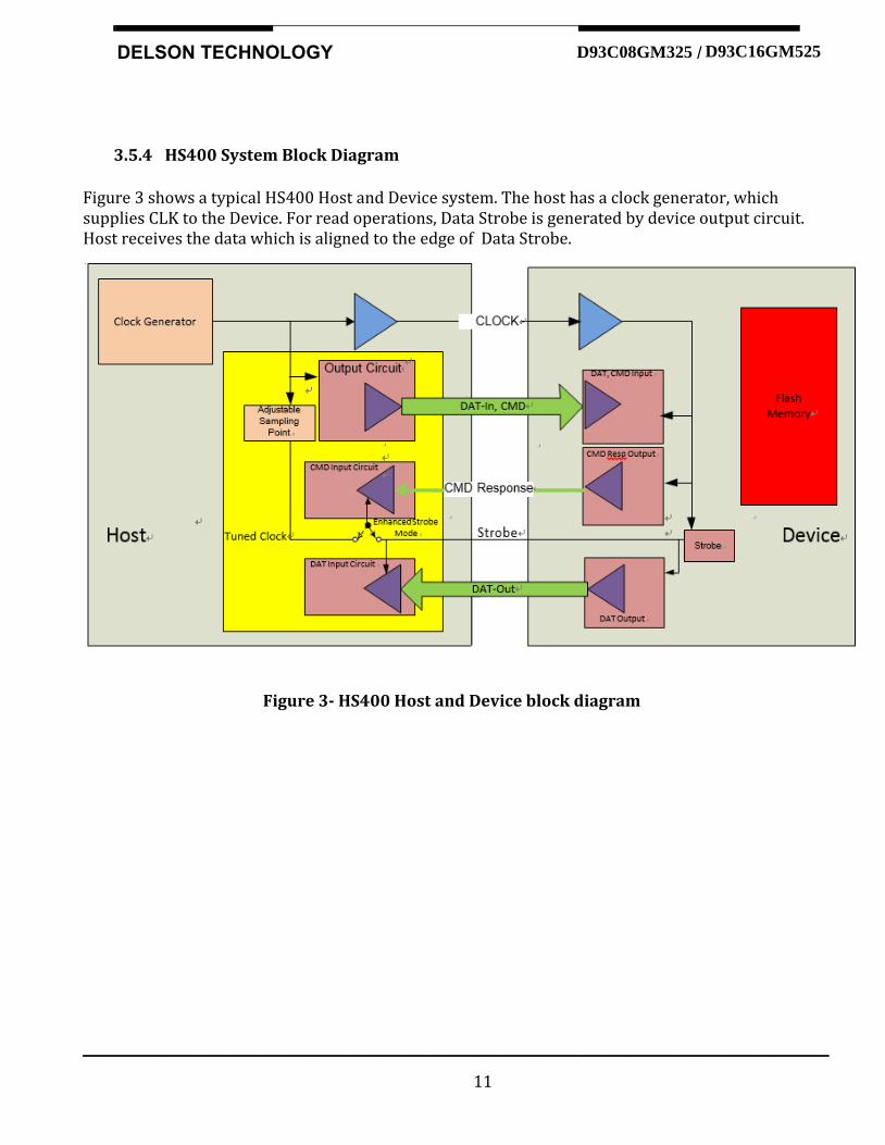
Figure 3 shows a typical HS400 Host and Device system. The host has a clock generator, which supplies CLK to the Device. For read operations, Data Strobe is generated by device output circuit. Host receives the data which is aligned to the edge of Data Strobe.
Figure 3- HS400 Host and Device block diagram
Internet
Data
Sheet DELSON TECHNOLOGY D93C08GM325 D93C16GM525 /
____________________________________________________________________________________________________________________
12
e•MMC™ 4.5
Flash Storage Specification
e•MMC™ 4.5 4. e•MMC™ Functional Description
4.1 e•MMC™ Overview
All communication between host and device are controlled by the host (main chip). The host sends a command, which results in a device response. For more details, refer to section 6.1 of the JEDEC Standard Specification No.JESD84-B51.
Five operation modes are defined for the e•MMC™ system:
• Boot operation mode • Device identification mode • Interrupt mode • Data transfer mode • Inactive mode
4.2 Boot Operation Mode
In boot operation mode, the master (e•MMC™ host) can read boot data from the slave (e•MMC™ device) by keeping CMD line low or sending CMD0 with argument + 0xFFFFFFFA, before issuing CMD1. The data can be read from either boot area or user area depending on register setting. For more details, refer to section 6.3 of the JEDEC Standard Specification No.JESD84-B51.
4.3 Device Identification Mode
While in device identification mode the host resets the device , validates operation voltage range and access mode, identifies the device and assigns a Relative device Address (RCA) to the device on the bus. All data communication in the Device Identification Mode uses the command line (CMD) only. For more details, refer to section 6.4 of the JEDEC Standard Specification No.JESD84-B51.
4.4 Interrupt Mode
The interrupt mode on the e•MMC™ system enables the master (e•MMC™ host) to grant the transmission allowance to the slaves (Device) simultaneously. This mode reduces the polling load for the host and hence, the power consumption of the system, while maintaining adequate responsiveness of the host to a Device request for service. Supporting e•MMC™ interrupt mode is an option, both for the host and the Device. For more details, refer to section 6.5 of the JEDEC Standard Specification No.JESD84-B51.
4.5 Data Transfer Mode
When the Device is in Stand-by State, communication over the CMD and DAT lines will be performed in push-pull mode. For more details, refer to section 6.6 of the JEDEC Standard Specification No.JESD84-B51.
Internet
Data
Sheet DELSON TECHNOLOGY D93C08GM325 D93C16GM525 /
____________________________________________________________________________________________________________________
13
Flash Storage Specification
e•MMC™ 4.5 4.6 Inactive Mode
The device will enter inactive mode if either the device operating voltage range or access mode is not valid. The device can also enter inactive mode with GO_INACTIVE_STATE command (CMD15). The device will reset to Pre-idle state with power cycle. For more details, refer to section 6.1 of the JEDEC Standard Specification No.JESD84-B51.
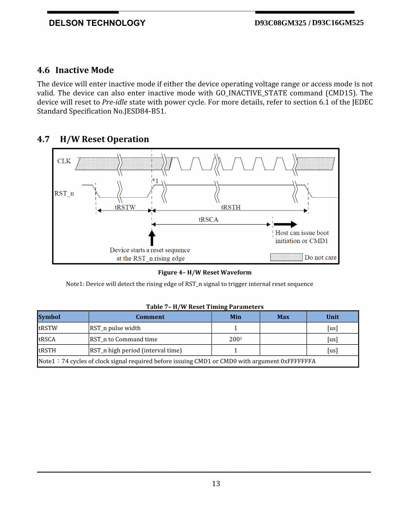
4.7 H/W Reset Operation
Figure 4– H/W Reset Waveform
Note1: Device will detect the rising edge of RST_n signal to trigger internal reset sequence
Table 7– H/W Reset Timing Parameters
Symbol Comment Min Max Unit
tRSTW RST_n pulse width 1 [us]
tRSCA RST_n to Command time 2001 [us]
tRSTH RST_n high period (interval time) 1 [us]
Note1:74 cycles of clock signal required before issuing CMD1 or CMD0 with argument 0xFFFFFFFA
Internet
Data
Sheet DELSON TECHNOLOGY D93C08GM325 D93C16GM525 /
____________________________________________________________________________________________________________________
14
Flash Storage Specification
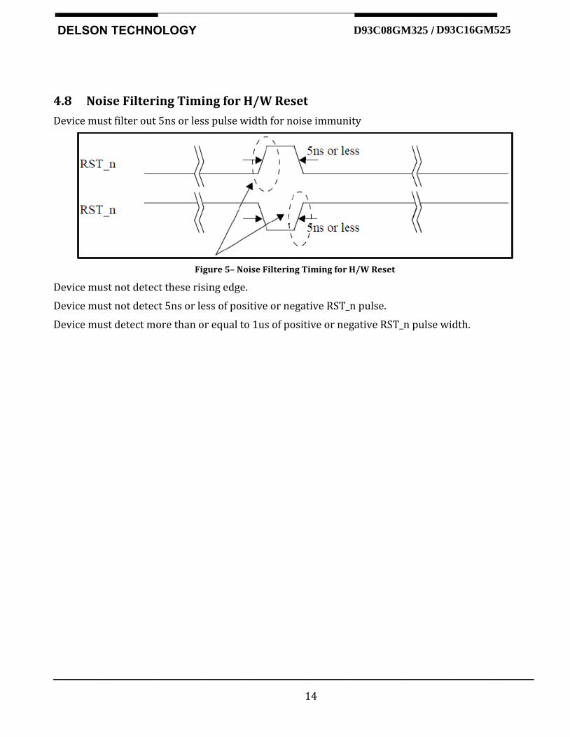
e•MMC™ 4.5 4.8 Noise Filtering Timing for H/W Reset
Device must filter out 5ns or less pulse width for noise immunity
Figure 5– Noise Filtering Timing for H/W Reset
Device must not detect these rising edge.
Device must not detect 5ns or less of positive or negative RST_n pulse.
Device must detect more than or equal to 1us of positive or negative RST_n pulse width.
Internet
Data
Sheet DELSON TECHNOLOGY D93C08GM325 D93C16GM525 /
____________________________________________________________________________________________________________________
15
e MMC™ 4.5
Flash Storage Specification
e•MMC™ 4.5 4.9 Field Firmware Update(FFU)
Field Firmware Updates (FFU) enables features enhancement in the field. Using this mechanism
the host downloads a new version of the firmware to the e.MMC device and, following a successful
download, instructs the e.MMC device to install the new downloaded firmware into the device.
In order to start the FFU process the host first checks if the e.MMC device supports FFU
capabilities by reading SUPPPORTED_MODES and FW_CONFIG fields in the EXT_CSD. If the e.MMC
device supports the FFU feature the host may start the FFU process. The FFU process starts by
switching to FFU Mode in MODE_CONFIG field in the EXT_CSD. In FFU Mode host should use closed-
ended or open ended commands for downloading the new firmware and reading vendor proprietary
data. In this mode, the host should set the argument of these commands to be as defined in FFU_ARG
field. In case these commands have a different argument the device behavior is not defined and the
FFU process may fail. The host should set Block Length to be DATA_SECTOR_SIZE. Downloaded
firmware bundle must be DATA_SECTOR_SIZE size aligned (internal padding of the bundle might be
required).Once in FFU Mode the host may send the new firmware bundle to the device using one or
more write commands.
The host could regain regular functionality of write and read commands by setting MODE_CONFIG
field in the EXT_CSD back to Normal state. Switching out of FFU Mode may abort the firmware
download operation. When host switched back to FFU Mode, the host should check the FFU Status to
get indication about the number of sectors which were downloaded successfully by reading the
NUMBER_OF_FW_SECTORS_CORRECTLY_PROGRAMMED in the extended CSD. In case the number of
sectors which were downloaded successfully is zero the host should re-start downloading the new
firmware bundle from its first sector. In case the number of sectors which were downloaded
successfully is positive the host should continue the download from the next sector, which would
resume the firmware download operation.
In case MODE_OPERATION_CODES field is not supported by the device the host sets to NORMAL
state and initiates a CMD0/HW_Reset/Power cycle to install the new firmware. In such case the
device doesn’t need to use NUMBER_OF_FW_SECTORS_CORRECTLY_PROGRAMMED.
In both cases occurrence of a CMD0/HW_Reset/Power occurred before the host successfully
downloaded the new firmware bundle to the device may cause the firmware download process to be
aborted.
Internet
Data
Sheet DELSON TECHNOLOGY D93C08GM325 D93C16GM525 /
____________________________________________________________________________________________________________________
16
e•MMC™ 4.5
Flash Storage Specification
e•MMC™ 4.5 4.10 Power off Notification for sleep
The host should notify the device before it powers the device off. This allows the device to better
prepare itself for being powered off. Power the device off means to turn off all its power supplies. In
particular, the host should issue a power off notification (POWER_OFF_LONG, POWER_OFF_SHORT )
if it intends to turn off both VCC and VCCQ power I or it may use to a power off notification
(SLEEP_NOTIFICATION ) if it intends to turn-off VCC after moving the device to Sleep state.
To indicate to the device that power off notification is supported by the host, a supporting host
shall first set the POWER_OFF_NOTIFICATION byte in EXT_CSD [34] to POWERED_ON (0x01). To
execute a power off, before powering the device down the host will changes the value to either
POWER_OFF_SHORT (0x02) or POWER_OFF_LONG (0x03). Host should waits for the busy line to be
de-asserted. Once the setting has changed to either 0x02 or 0x03, host may safely power off the
device.
The host may issue SLEEP_AWAKE (CMD5) to enter or to exit from Sleep state if
POWER_OFF_NOTIFICATION byte is set to POWERED_ON. Before moving to Standby state and then
to Sleep state, the host sets POWER_OFF_NOTIFICATION to SLEEP_NOTIFICATION and waits for the
DAT0 line de-assertion. While in Sleep (slp) state VCC (Memory supply) may be turned off as defined
in 4.1.6. Removing power supplies other than VCC while the device is in the Sleep (slp) state may
result in undefined device behavior. Before removing all power supplies, the host should transition
the device out of Sleep (slp) state back to Transfer state using CMD5 and CMD7 and then execute a
power off notification setting POWER_OFF_NOTIFICATION byte to either POWER_OFF_SHORT or
POWER_OFF_LONG.
If host continues to send commands to the device after switching to the power off setting (POWER
_OFF_LONG, POWER_OFF_SHORT or SLEEP_NOTIFICATION) or performs HPI during its busy conditio
n, the device shall restore the POWER_OFF_NOTIFICATION byte to POWERED_ON.
If host tries to change POWER_OFF_NOTIFICATION to 0x00 after writing another value there, a SWIT
CH_ERROR is generated.
The difference between the two power-off modes is how urgent the host wants to turn power off.
The device should respond to POWER_OFF_SHORT quickly under the generic CMD6 timeout. If more t
ime is acceptable, POWER_OFF_LONG may be used and the device shall respond to it within the POW
ER_OFF_LONG_TIME timeout.
While POWER_OFF_NOTIFICATION is set to POWERED_ON, the device expects the host to host shall:
•Keep the device power supplies alive (both VCC and VCCQ) and in their active mode
•Not power off the device intentionally before changing POWER_OFF_NOTIFICATION to either
POWER_OFF_LONG or POWER_OFF_SHORT
Internet
Data
Sheet DELSON TECHNOLOGY D93C08GM325 D93C16GM525 /
____________________________________________________________________________________________________________________
17
e•MMC™ 4.5
Flash Storage Specification
e•MMC™ 4.5 •Not power off VCC intentionally before changing POWER_OFF_NOTIFICATION to
SLEEP_NOTIFICATION and before moving the device to Sleep state
Before moving to Sleep state hosts may set the POWER_OFF_NOTIFICATION byte to
SLEEP_NOTIFICATION (0x04) if aware that the device is capable of autonomously initiating
background operations for possible performance improvements. Host should wait for the busy line to
be de-asserted. Busy line may be asserted up the period defined in SLEEP_NOTIFICATION_TIME byte
in EXT_CSD [216]. Once the setting has changed to 0x04 host may set the device into Sleep mode
(CMD7+CMD5). After getting out from Sleep the POWER_OFF_NOTIFICATION byte will restore its
value to POWERED_ON. HPI may interrupt the SLEEP_NOTIFICATION operation. In that case
POWER_OFF_NOTIFICATION byte will restore to POWERED_ON.
4.11 Cache Enhancement Barrier
Barrier function provides a way to perform a delayed in-order flushing of a cached data. The
main motivation for using barrier commands is to avoid the long delay that is introduced by flush
commands. There are cases where the host is not interested in flushing the data right away, however
it would like to keep an order between different cached data batches. The barrier command enables
the host achieving the in-order goal but without paying the flush delay, since the real flushing can be
delayed by the device to some later idle time. The formal definition of the barrier rule is as follows:
Denote a sequence of requests Ri, i=0,..,N. Assuming a barrier is set between requests Rx and
Rx+1 (0<x<N) then all the requests R0..Rx must be flushed to the non-volatile memory before any of
the requests Rx+1..RN.
Between two barriers the device is free to write data into the non-volatile memory in any order.
If the host wants to preserve a certain order it shall flush the cache or set another barrier at a point
where order is important.
The barrier is set by writing to the BARRIER bit of the FLUSH_CACHE byte (EXT_CSD byte [32]).
Any error resulted can be read from the status register by CMD13 after the completion of the
programming as defined for a normal write request. The error could affect any data written to the
cache since the previous flush operation.
The device shall support any number of barrier commands between two flush commands. In
case of multiple barrier commands between two flush commands a subset of the cached data may be
committed to the non-volatile memory according to the barrier rule. Internally, a device may have an
upper limit on the barrier amount it can absorb without flushing the cache. That is, if the host
exceeds this barrier amount, the device may issue, internally, a normal flush.
Internet
Data
Sheet DELSON TECHNOLOGY D93C08GM325 D93C16GM525 /
____________________________________________________________________________________________________________________
18
Flash Storage Specification
e•MMC™ 4.5 The device shall expose its barrier support capability via the BARRIER_SUPPORT byte (EXT_CSD
byte [486]). If a device does not support barrier function this register shall be zero. If a device
supports barrier function this register shall be one.
Assuming the device supports barrier function, if the BARRIER bit of the FLUSH_CACHE byte is
set, a barrier operation shall be executed.
If the cache gets totally full and/or the cache is not able to receive the data of the next access
(per block count indicated in CMD23 or per initiated single / open ended multiple block write in
general) then it shall still be the responsibility of the e•MMC device to store the data of the next
access within the timeouts that are specified elsewhere in this specification. The actual algorithm to
handle the new data and possible flush of some older cached data is left for the implementation.
Note: When issuing a force-programming write request (CMD23 with bit 24 on) or a reliable
write request (CMD23 with bit 31 on), the host should be aware that the data will be written to the
non-volatile memory, potentially, before any cached data, even if a barrier command was issued.
Therefore, if the writing order to the non-volatile memory is important, it is the responsibility of the
host to issue a flush command before the force-programming or the reliable-write request.
In order to use the barrier function, the host shall set bit 0 of BARRIER_EN (EXT_CSD byte [31]).
The barrier feature is optional for an e•MMC device.
Internet
Data
Sheet DELSON TECHNOLOGY D93C08GM325 D93C16GM525 /
____________________________________________________________________________________________________________________
19
Flash Storage Specification
e•MMC™ 4.5 4.12 Cache Flushing Policy
The host may require the device to flush data from the cache in an in-order manner. From time
to time, to guarantee in-order flushing, the host may command the device to flush the device cache or
may use a barrier command.
However, if the e•MMC device flushing policy is to flush data from the cache in an in-order
manner, cache barrier commands or flush commands operations (In case goal is to guarantee the
flushing order) are redundant and impose a needless overhead to the device and host.
FIFO bit in CACHE_FLUSH_POLICY field (EXT_CSD byte [240]) is used by the device to indicate to
the host that the device cache flushing policy is First-In-First-Out; this means that the device
guarantees that the order of the flushing of data would be the in same order which data was written
to the cache. When the FIFO bit is set it is recommended for the host not to send cache barrier
commands or flush operations which goal is to guarantee the flushing order as they are redundant
and impose a burden to the system.
However, if the FIFO bit is set to 1b and the device supports the cache barrier mechanism, the
host may still send barrier commands without getting an error. Sending these commands will not
change the device behavior as device flushes cache in-order anyway.
The CACHE_FLUSH_POLICY field is read-only field and never change its value either by the host
or device.
Internet
Data
Sheet DELSON TECHNOLOGY D93C08GM325 D93C16GM525 /
____________________________________________________________________________________________________________________
20
e•MMC™ 4.5 4.13 Command Queueing
To facilitate command queuing in e•MMC, the device manages an internal task queue to which
the host can queue data transfer tasks.
Initially the task queue is empty. Every task is issued by the host and initially queued as pending.
The device controller works to prepare pending tasks for execution. When a task is ready for
execution its state changes to “ready for execution”. The exact meaning of “ready for execution” is left
for device implementation.
The host tracks the state of all queued tasks and may order the execution of any task, which is
marked as “ready for execution” by sending a command indicating its task ID. When the execute
command is received (CMD46/CMD47) the device executes the data transfer transaction.
For example, in order to queue a write transaction the host sends a CMD44 indicating the task’s
parameters. The device responds and the host sends a CMD45, indicating the start block address.
The device regards the two commands as a single task in the queue and sends a response
indicating success if no error is detected. This exchange may be executed on the CMD line while a
data transfer, or busy state, is ongoing on the DAT lines. The host tracks the state of the queue using
CMD13.
At a later time, when data transfer is not in progress, the host issues a CMD47, ordering the
device to execute a task from the queue, providing the Task ID in its argument. The device responds
with an R1 response and the data transfer starts.
Note that if hosts need to access RPMB partition, the host should disable the Command Queue
mechanism and access RPMB partition not through the command queue.
General Purpose partitions may be accessed when command queueing is enabled.
The queue must be empty when CMD6 is sent (to switch partitions or to disable command
queueing).
Sending CMD6 while the queue is not empty shall be regarded as illegal command (as explained
6.6.42.9 Supported Commands).
Prior to enabling command queuing, the block size shall be set to 512B. Device may respond
with an error to CMD46/CMD47 if block size is not 512B.
Internet
Data
Sheet DELSON TECHNOLOGY D93C08GM325 D93C16GM525 /
____________________________________________________________________________________________________________________
21
e•MMC™ 4.5
Flash Storage Specification
e•MMC™ 4.5 5. Register Settings
Within the Device interface six registers are defined: OCR, CID, CSD, EXT_CSD, RCA and DSR. These can be accessed only by corresponding commands (see Section 6.10 of JESD84-B51).
5.1. OCR Register
The 32-bit operation conditions register (OCR) stores the VDD voltage profile of the Device and the access mode indication. In addition, this register includes a status information bit. This status bit is set if the Device power up procedure has been finished. The OCR register shall be implemented by all Devices.
5.2. CID Register
The Card Identification (CID) register is 128 bits wide. It contains the Device identification information used during the Device identification phase (e•MMC™ protocol). For details, refer to JEDEC Standard Specification No.JESD84-B51
5.3. CSD Register
The Card-Specific Data (CSD) register provides information on how to access the contents stored in e•MMC™. The CSD registers are used to define the error correction type, maximum data access time, data transfer speed, data format…etc. For details, refer to section 7.3 of the JEDEC Standard Specification No.JESD84-B51.
5.4. Extended CSD Register
The Extended CSD register defines the Device properties and selected modes. It is 512 bytes long. The most significant 320 bytes are the Properties segment, which defines the Device capabilities and cannot be modified by the host. The lower 192 bytes are the Modes segment, which defines the configuration the Device is working in. These modes can be changed by the host by means of the SWITCH command. For details, refer to section 7.4 of the JEDEC Standard Specification No.JESD84-B51.
5.5. RCA Register
The writable 16-bit Relative Device Address (RCA) register carries the Device address assigned by the host during the Device identification. This address is used for the addressed host-Device communication after the Device identification procedure. The default value of the RCA register is 0x0001. The value 0x0000 is reserved to set all Devices into the Stand-by State with CMD7. For detailed register setting value, please refer to appendix or KSI FAE.
5.6. DSR Register
The 16-bit driver stage register (DSR) is described in detail in Section 7.6 of the JEDEC Standard Specification No.JESD84-B51. It can be optionally used to improve the bus performance for extended operating conditions (depending on parameters like bus length, transfer rate or number of Devices). The CSD register carries the information about the DSR register usage. For detailed register setting value, please refer to appendix or KSI FAE.
Internet
Data
Sheet DELSON TECHNOLOGY D93C08GM325 D93C16GM525 /
____________________________________________________________________________________________________________________
22
Flash Storage Specification
e•MMC™ 4.5
Flash Storage Specification
e•MMC™ 4.5 6. The e•MMC™ bus
The e•MMC™ bus has ten communication lines and three supply lines:
• CMD: Command is a bidirectional signal. The host and Device drivers are operating in two
modes, open drain and push/pull. • DAT0-7: Data lines are bidirectional signals. Host and Device drivers are operating in
push-pull mode • CLK: Clock is a host to Device signal. CLK operates in push-pull mode
• Data Strobe: Data Strobe is a Device to host signal. Data Strobe operates in push-pull mode.
Figure 6– Bus Circuitry Diagram
The ROD is switched on and off by the host synchronously to the open-drain and push-pull mode transitions. The host does not have to have open drain drivers, but must recognize this mode to switch on the ROD. RDAT and RCMD are pull-up resistors protecting the CMD and the DAT lines against bus floating device when all device drivers are in a high-impedance mode.
A constant current source can replace the ROD by achieving a better performance (constant slopes for the signal rising and falling edges). If the host does not allow the switchable ROD implementation, a fixed RCMD can be used).Consequently the maximum operating frequency in the open drain mode has to be reduced if the used RCMD value is higher than the minimal one given in . RData strobe is pull-down resistor used in HS400 device .
Internet
Data
Sheet DELSON TECHNOLOGY D93C08GM325 D93C16GM525 /
____________________________________________________________________________________________________________________
23
e•MMC™ 4.5
Flash Storage Specification
e•MMC™ 4.5 6.1 Power-up
6.1.1 e•MMC™ power-up
An e•MMC™ bus power-up is handled locally in each device and in the bus master. Figure7 shows the power-up sequence and is followed by specific instructions regarding the power-up sequence. Refer to section 10.1 of the JEDEC Standard Specification No.JESD84-B51 for specific instructions regarding the power-up sequence.
Figure 7 – e•MMC™ Power-up Diagram
Internet
Data
Sheet DELSON TECHNOLOGY D93C08GM325 D93C16GM525 /
____________________________________________________________________________________________________________________
24
Flash Storage Specification
e•MMC™ 4.5 6.1.2 e•MMC™ Power Cycling
The master can execute any sequence of VCC and VCCQ power-up/power-down. However, the master must not issue any commands until VCC and VCCQ are stable within each operating voltage range. After the slave enters sleep mode, the master can power-down VCC to reduce power consumption. It is necessary for the slave to be ramped up to VCC before the host issues CMD5 (SLEEP_AWAKE) to wake the slave unit. For more information about power cycling see Section 10.1.3 of the JEDEC Standard Specification No.JESD84-B51.
Figure 8– The e•MMC™ Power Cycle
Internet
Data
Sheet DELSON TECHNOLOGY D93C08GM325 D93C16GM525 /
____________________________________________________________________________________________________________________
25
Flash Storage Specification
e•MMC™ 4.5 6.2 Bus Operating Conditions
Table 8– General Operating Conditions
Parameter Symbol Min Max. Unit Remark
Peak voltage on all lines -0.5 VCCQ +
0.5 V
All Inputs
Input Leakage Current (before initialization sequence and/or the internal pull up resistors connected)
-100 100 μA
Input Leakage Current (after initialization sequence and the internal pull up resistors disconnected)
-2 2 μA
All Outputs
Output Leakage Current (before initialization sequence) -100 100 μA
Output Leakage Current (after initialization sequence) -2 2 μA
Note1:Initialization sequence is defined in section 10.1
6.2.1 Power supply: e•MMC™
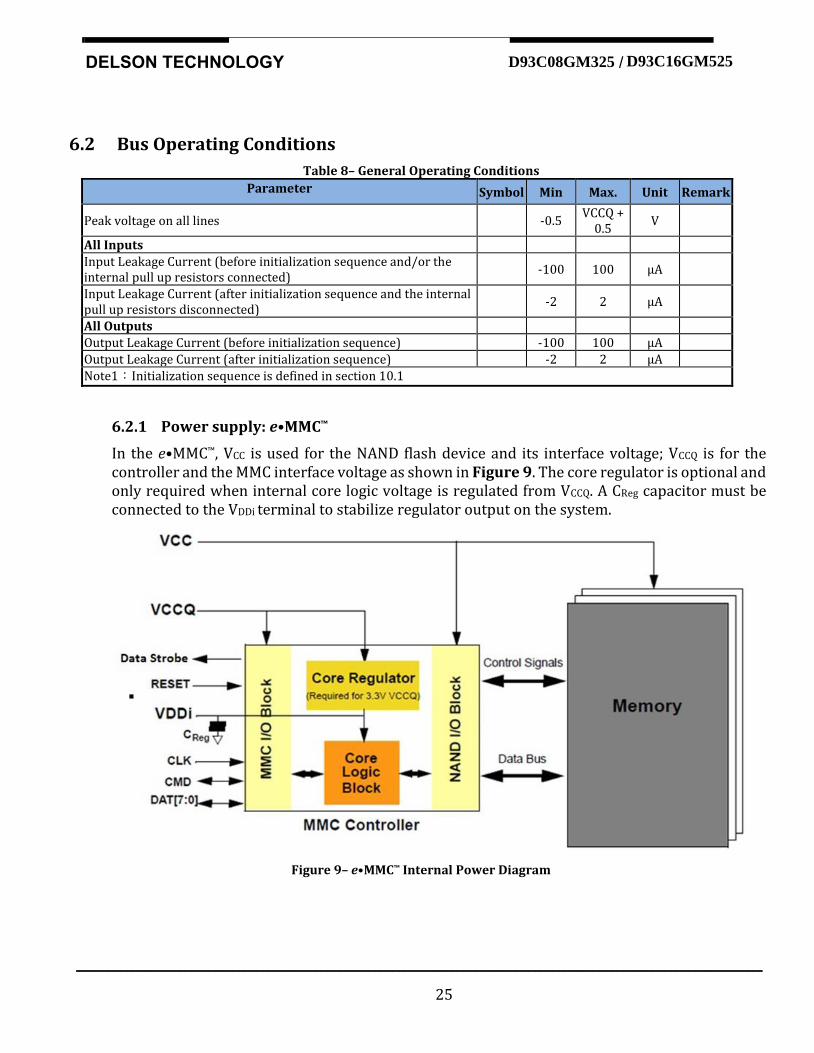
In the e•MMC™, VCC is used for the NAND flash device and its interface voltage; VCCQ is for the controller and the MMC interface voltage as shown in Figure 9. The core regulator is optional and only required when internal core logic voltage is regulated from VCCQ. A CReg capacitor must be connected to the VDDi terminal to stabilize regulator output on the system.
Figure 9– e•MMC™ Internal Power Diagram
Internet
Data
Sheet DELSON TECHNOLOGY D93C08GM325 D93C16GM525 /
____________________________________________________________________________________________________________________
26
e•MMC™ 4.5 6.2.2 e•MMC™ Power Supply Voltage
The e•MMC™ supports one or more combinations of VCC and VCCQ as shown in Table9. The VCCQ must be defined at equal to or less than VCC.
Table 9– e•MMC™ Operating Voltage
Parameter Symbol MIN MAX Unit Remarks
Supply voltage (NAND) VCC 2.7 3.6 V
Supply voltage (I/O) VCCQ 2.7 3.6 V
1.7 1.95 V
Supply power-up for 3.3V tPRUH 35 ms
Supply power-up for 1.8V tPRUL 25 ms
The e•MMC™ must support at least one of the valid voltage configurations, and can optionally support all valid voltage configurations (see Table ).
Table 10 – e•MMC™ Voltage Combinations
VCCQ
1.7V–1.95V 2.7V–3.6V1
Vcc 2.7V-3.6V Valid Valid
Note1:VCCQ (I/O) 3.3 volt range is not supported in HS200 /HS400 devices
Internet
Data
Sheet DELSON TECHNOLOGY D93C08GM325 D93C16GM525 /
____________________________________________________________________________________________________________________
27
Flash Storage Specification
e•MMC™ 4.5 6.2.3 Bus Signal Line Load
The total capacitance CL of each line of the e•MMC™ bus is the sum of the bus master capacitance CHOST, the bus capacitance CBUS itself and the capacitance CDEVICE of e•MMC™ connected to this line:
CL = CHOST + CBUS + CDEVICE
The sum of the host and bus capacitances must be under 20pF.
Table 11– Signal Line Load
Parameter Symbol Min Max Unit Remark Pull-up resistance for CMD
RCMD 4.7 50 Kohm to prevent bus floating
Pull-up resistance for DAT0–7
RDAT 10 50 Kohm to prevent bus floating
Pull-up resistance for RST_n
RRST_n 4.7 50 Kohm
It is not necessary to put pull-up resistance on RST_n (H/W rest) line if host does not use H/W reset. (Extended CSD register [162] = 0 b )
Bus signal line capacitance
CL 30 pF Single Device
Single Device capacitance CBGA 12 pF Maximum signal line inductance
16 nH
Impedance on CLK / CMD / DAT0~7
45 55 ohm Impedance match
Serial’s resistance on CLK line
SRCLK 0 47 ohm
Serial’s resistance on CMD / DAT0~7 line
SRCMD SRDAT0~7
0 47 ohm
VCCQ decoupling capacitor
2.2+0.1 4.7+0.22
μF
It should be located as close as possible to the balls defined in order to minimize connection parasitic
CH1 1 2.2
CH1 is only for HS200. It should be placed adjacent to VCCQ-VSSQ balls (#K6 and #K4 accordingly, next to DAT [7..0] balls). It should be located as close as possible to the balls defined in order to minimize connection parasitic.
VCC capacitor value 1+0.1 4.7+0.22 μF It should be located as close as possible to the balls defined in order to minimize connection parasitic
VDDi capacitor value CREG 1 4.7+0.1 μF
To stabilize regulator output to controller core logics. It should be located as close as possible to the balls defined in order to minimize connection parasitic
Internet
Data
Sheet DELSON TECHNOLOGY D93C08GM325 D93C16GM525 /
____________________________________________________________________________________________________________________
28
Flash Storage Specification
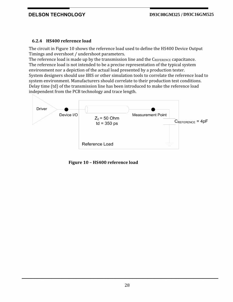
e•MMC™ 4.5 6.2.4 HS400 reference load
The circuit in Figure 10 shows the reference load used to define the HS400 Device Output Timings and overshoot / undershoot parameters. The reference load is made up by the transmission line and the CREFERENCE capacitance. The reference load is not intended to be a precise representation of the typical system environment nor a depiction of the actual load presented by a production tester. System designers should use IBIS or other simulation tools to correlate the reference load to system environment. Manufacturers should correlate to their production test conditions. Delay time (td) of the transmission line has been introduced to make the reference load independent from the PCB technology and trace length.
Figure 10 – HS400 reference load
Internet
Data
Sheet DELSON TECHNOLOGY D93C08GM325 D93C16GM525 /
____________________________________________________________________________________________________________________
29
e•MMC™ 4.5
Flash Storage Specification
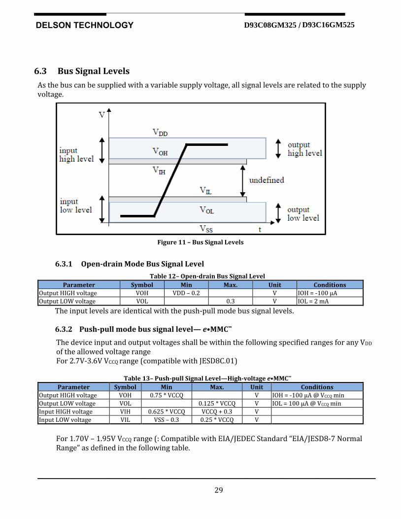
e•MMC™ 4.5 6.3 Bus Signal Levels
As the bus can be supplied with a variable supply voltage, all signal levels are related to the supply voltage.
Figure 11 – Bus Signal Levels
6.3.1 Open-drain Mode Bus Signal Level
Table 12– Open-drain Bus Signal Level
Parameter Symbol Min Max. Unit Conditions Output HIGH voltage VOH VDD – 0.2 V IOH = -100 μA
Output LOW voltage VOL 0.3 V IOL = 2 mA
The input levels are identical with the push-pull mode bus signal levels. 6.3.2 Push-pull mode bus signal level— e•MMC™
The device input and output voltages shall be within the following specified ranges for any VDD of the allowed voltage range For 2.7V-3.6V VCCQ range (compatible with JESD8C.01)
Table 13– Push-pull Signal Level—High-voltage e•MMC™
Parameter Symbol Min Max. Unit Conditions
Output HIGH voltage VOH 0.75 * VCCQ V IOH = -100 μA @ VCCQ min
Output LOW voltage VOL 0.125 * VCCQ V IOL = 100 μA @ VCCQ min
Input HIGH voltage VIH 0.625 * VCCQ VCCQ + 0.3 V
Input LOW voltage VIL VSS – 0.3 0.25 * VCCQ V
For 1.70V – 1.95V VCCQ range (: Compatible with EIA/JEDEC Standard “EIA/JESD8-7 Normal Range” as defined in the following table.
Internet
Data
Sheet DELSON TECHNOLOGY D93C08GM325 D93C16GM525 /
____________________________________________________________________________________________________________________
30
Flash Storage Specification
e•MMC™ 4.5 Table 14– Push-pull Signal Level—1.70 -1.95 VCCQ Voltage Range
Parameter Symbol Min Max. Unit Conditions
Output HIGH voltage VOH VCCQ – 0.45V V IOH = -2mA
Output LOW voltage VOL 0.45V V IOL = 2mA
Input HIGH voltage VIH 0.65 * VCCQ 1 VCCQ + 0.3 V
Input LOW voltage VIL VSS – 0.3 0.35 * VDD2 V
Note1:0.7 * VDD for MMC™4.3 and older revisions.
Note2:0.3 * VDD for MMC™4.3 and older revisions.
6.3.3 Bus Operating Conditions for HS200 & HS400
The bus operating conditions for HS200 devices is the same as specified in sections 10.5.1 of JESD84-B51through 10.5.2 of JESD84-B51. The only exception is that VCCQ=3.3v is not supported. 6.3.4 Device Output Driver Requirements for HS200 & HS400
Refer to section 10.5.4 of the JEDEC Standard Specification No.JESD84-B51.
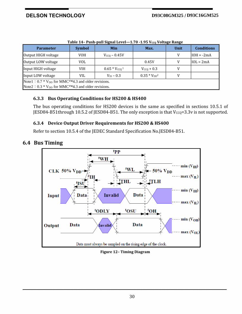
6.4 Bus Timing
Figure 12– Timing Diagram
Internet
Data
Sheet DELSON TECHNOLOGY D93C08GM325 D93C16GM525 /
____________________________________________________________________________________________________________________
31
Flash Storage Specification
e•MMC™ 4.5 6.4.1 Device Interface Timings
Table 15– High-speed Device Interface Timing
Parameter Symbol Min Max. Unit Remark
Clock CLK1 Clock frequency Data Transfer Mode (PP)2
fPP 0 523 MHz CL ≤ 30 pF Tolerance:+100KHz
Clock frequency Identification Mode (OD)
fOD 0 400 kHz Tolerance: +20KHz
Clock high time tWH 6.5 ns CL ≤ 30 pF
Clock low time tWL 6.5 ns CL ≤ 30 pF
Clock rise time4 tTLH 3 ns CL ≤ 30 pF
Clock fall time tTHL 3 ns CL ≤ 30 pF
Inputs CMD, DAT (referenced to CLK) Input set-up time tISU 3 ns CL ≤ 30 pF
Input hold time tIH 3 ns CL ≤ 30 pF
Outputs CMD, DAT (referenced to CLK)
Output delay time during data transfer tODLY 13.7 ns CL ≤ 30 pF
Output hold time tOH 2.5 ns CL ≤ 30 pF
Signal rise time5 tRISE 3 ns CL ≤ 30 pF
Signal fall time tFALL 3 ns CL ≤ 30 pF
Note1:CLK timing is measured at 50% of VDD.
Note2: eMMC™ shall support the full frequency range from 0-26Mhz or 0-52MHz
Note3:Device can operate as high-speed Device interface timing at 26 MHz clock frequency.
Note4:CLK rise and fall times are measured by min (VIH) and max (VIL).
Note5:Inputs CMD DAT rise and fall times are measured by min (VIH) and max (VIL) and outputs CMD DAT rise and
fall times are measured by min (VOH) and max (VOL). “
Table16– Backward-compatible Device Interface Timing
Parameter Symbol Min Max. Unit Remark1
Clock CLK2
Clock frequency Data Transfer Mode (PP)3 fPP 0 26 MHz CL ≤ 30 pF
Clock frequency Identification Mode (OD) fOD 0 400 kHz
Clock high time tWH 10 CL ≤ 30 pF
Clock low time tWL 10 ns CL ≤ 30 pF
Clock rise time4 tTLH 10 ns CL ≤ 30 pF
Clock fall time tTHL 10 ns CL ≤ 30 pF
Inputs CMD, DAT (referenced to CLK) Input set-up time tISU 3 ns CL ≤ 30 pF
Input hold time tIH 3 ns CL ≤ 30 pF
Outputs CMD, DAT (referenced to CLK)
Output set-up time5 tOSU 11.7 ns CL ≤ 30 pF
Output hold time5 tOH 8.3 ns CL ≤ 30 pF
Note1:The Device must always start with the backward-compatible interface timing. The timing mode can be switched
to high-speed interface timing by the host sending the SWITCH command (CMD6) with the argument for high-speed interface select.
Note2:CLK timing is measured at 50% of VDD.
Internet
Data
Sheet DELSON TECHNOLOGY D93C08GM325 D93C16GM525 /
____________________________________________________________________________________________________________________
32
Flash Storage Specification
e•MMC™ 4.5 Note3:For compatibility with Devices that support the v4.2 standard or earlier, host should not use > 26 MHz before
switching to high-speed interface timing. Note4:CLK rise and fall times are measured by min (VIH) and max (VIL).
Note5:tOSU and tOH are defined as values from clock rising edge. However, there may be Devices or devices which
utilize clock falling edge to output data in backward compatibility mode. Therefore, it is recommended for hosts either to settWL value as long as possible within the range which will not go over tCK-tOH(min) in the system or to use slow clock frequency, so that host could have data set up margin for those devices. In this case, each device which utilizes clock falling edge might show the correlation either between tWL and tOSU or between tCK and tOSU for the device in its own datasheet as a note or its application notes.
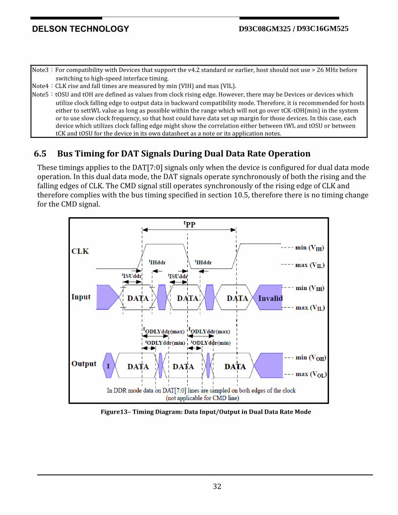
6.5 Bus Timing for DAT Signals During Dual Data Rate Operation
These timings applies to the DAT[7:0] signals only when the device is configured for dual data mode operation. In this dual data mode, the DAT signals operate synchronously of both the rising and the falling edges of CLK. The CMD signal still operates synchronously of the rising edge of CLK and therefore complies with the bus timing specified in section 10.5, therefore there is no timing change for the CMD signal.
Figure13– Timing Diagram: Data Input/Output in Dual Data Rate Mode
Internet
Data
Sheet DELSON TECHNOLOGY D93C08GM325 D93C16GM525 /
____________________________________________________________________________________________________________________
33
e MMC™ 4.5
Flash Storage Specification
e•MMC™ 4.5 6.5.1 Dual Data Rate Interface Timings
Table 17– High-speed Dual Data Rate Interface Timing
Parameter Symbol Min Max. Unit Remark
Input CLK1
Clock duty cycle 45 55 % Includes jitter, phase noise
Input DAT (referenced to CLK-DDR mode)
Input set-up time tISUddr 2.5 ns CL ≤ 20 pF
Input hold time tIHddr 2.5 ns CL ≤ 20 pF
Output DAT (referenced to CLK-DDR mode)
Output delay time during data transfer tODLYddr 1.5 7 ns CL ≤ 20 pF
Signal rise time (all signals)2 tRISE 2 ns CL ≤ 20 pF
Signal fall time (all signals) tFALL 2 ns CL ≤ 20 pF
Note1:CLK timing is measured at 50% of VDD.
Note2:Inputs CMD, DAT rise and fall times are measured by min (VIH) and max (VIL), and outputs CMD, DAT rise and
fall times are measured by min (VOH) and max (VOL)
6.6 Bus Timing Specification in HS200 Mode
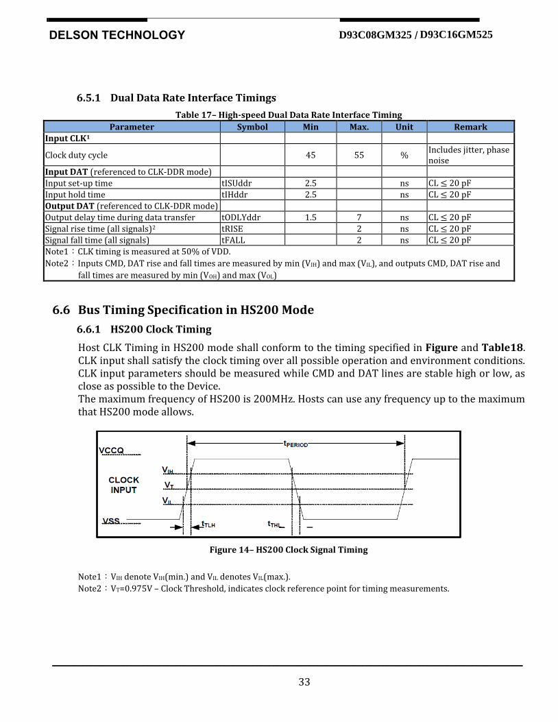
6.6.1 HS200 Clock Timing
Host CLK Timing in HS200 mode shall conform to the timing specified in Figure and Table18. CLK input shall satisfy the clock timing over all possible operation and environment conditions. CLK input parameters should be measured while CMD and DAT lines are stable high or low, as close as possible to the Device. The maximum frequency of HS200 is 200MHz. Hosts can use any frequency up to the maximum that HS200 mode allows.
Figure 14– HS200 Clock Signal Timing
Note1:VIH denote VIH(min.) and VIL denotes VIL(max.).
Note2:VT=0.975V – Clock Threshold, indicates clock reference point for timing measurements.
Internet
Data
Sheet DELSON TECHNOLOGY D93C08GM325 D93C16GM525 /
____________________________________________________________________________________________________________________
34
e•MMC™ 4.5
Flash Storage Specification
e•MMC™ 4.5 Table18– HS200 Clock Signal Timing
Symbol Min. Max. Unit Remark
tPERIOD 5 - ns 200MHz (Max.), between rising edges
tTLH, tTHL - 0.2*
tPERIOD ns
tTLH, tTHL < 1ns (max.) at 200MHz, CBGA=12pF, The absolute maximum value of tTLH, tTHL is 10ns regardless of clock frequency.
Duty Cycle 30 70 %
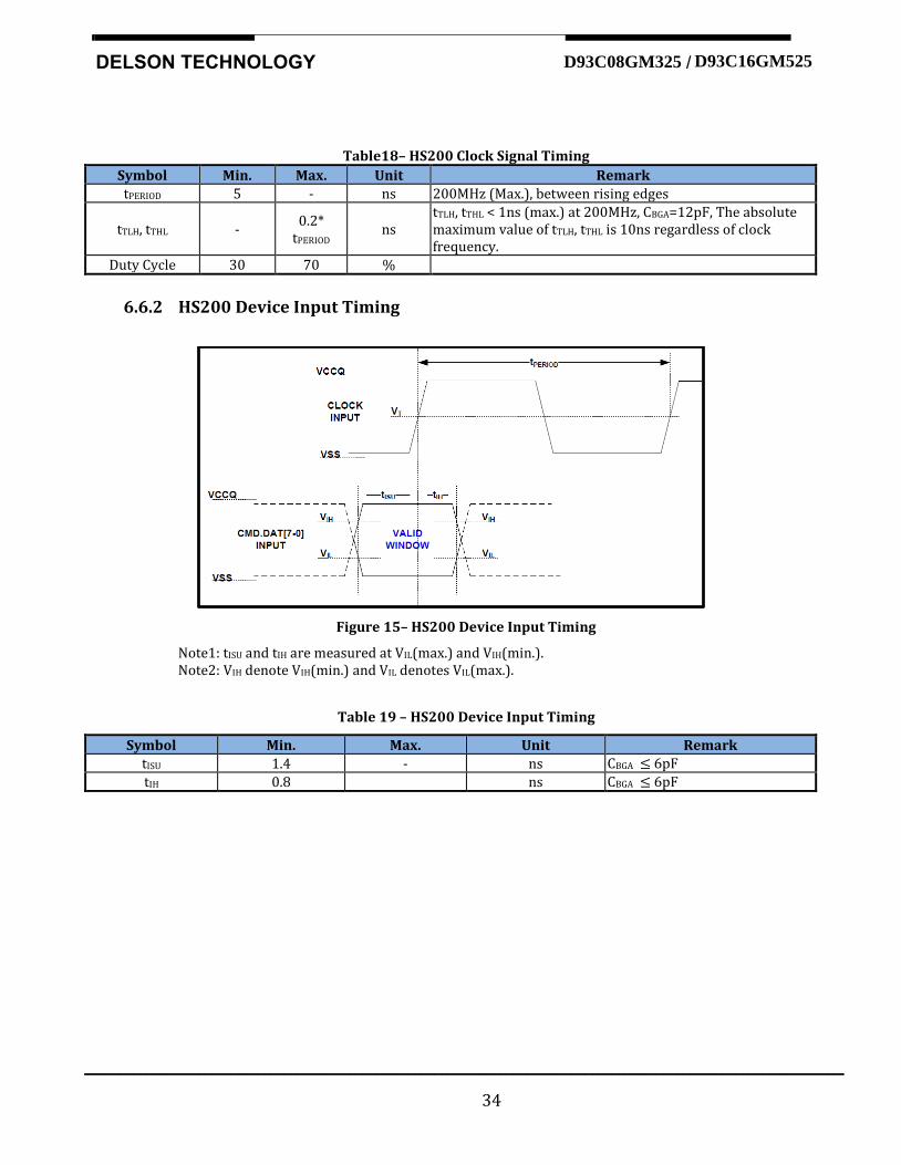
6.6.2 HS200 Device Input Timing
Figure 15– HS200 Device Input Timing
Note1: tISU and tIH are measured at VIL(max.) and VIH(min.). Note2: VIH denote VIH(min.) and VIL denotes VIL(max.).
Table 19 – HS200 Device Input Timing
Symbol Min. Max. Unit Remark
tISU 1.4 - ns CBGA ≤ 6pF
tIH 0.8 ns CBGA ≤ 6pF
Internet
Data
Sheet DELSON TECHNOLOGY D93C08GM325 D93C16GM525 /
____________________________________________________________________________________________________________________
35
e MMC™ 4.5
Flash Storage Specification
e•MMC™ 4.5 6.6.3 HS200 Device Output Timing
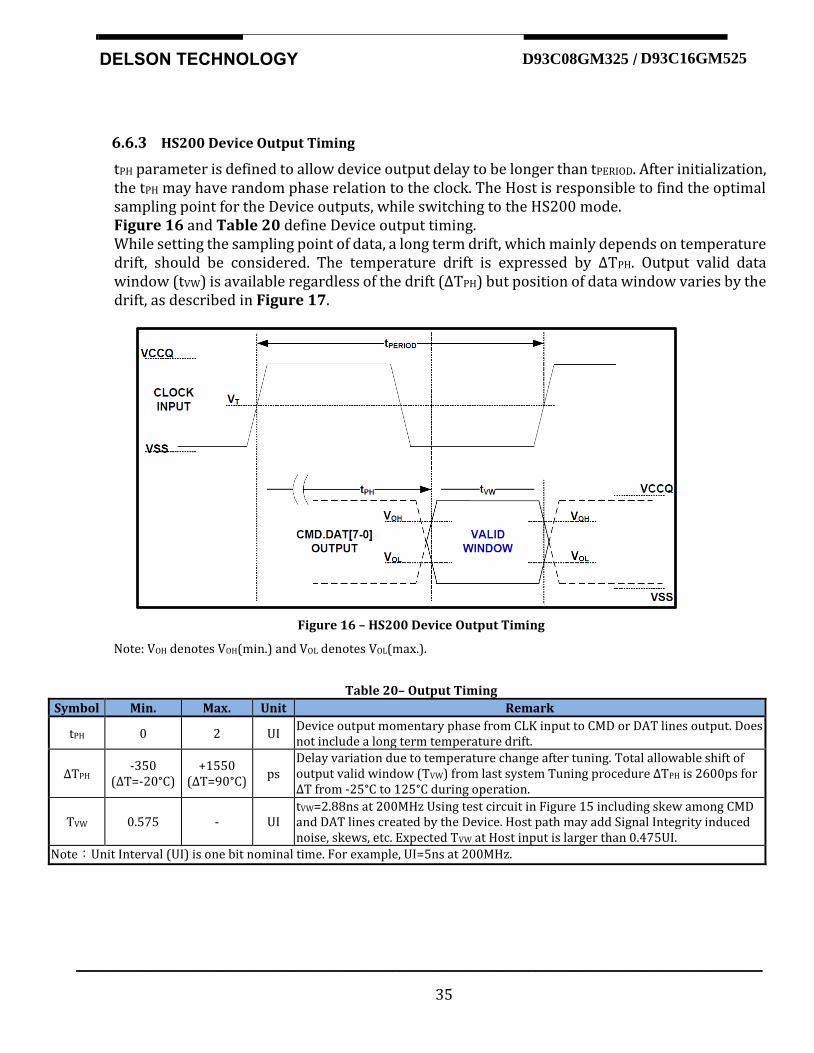
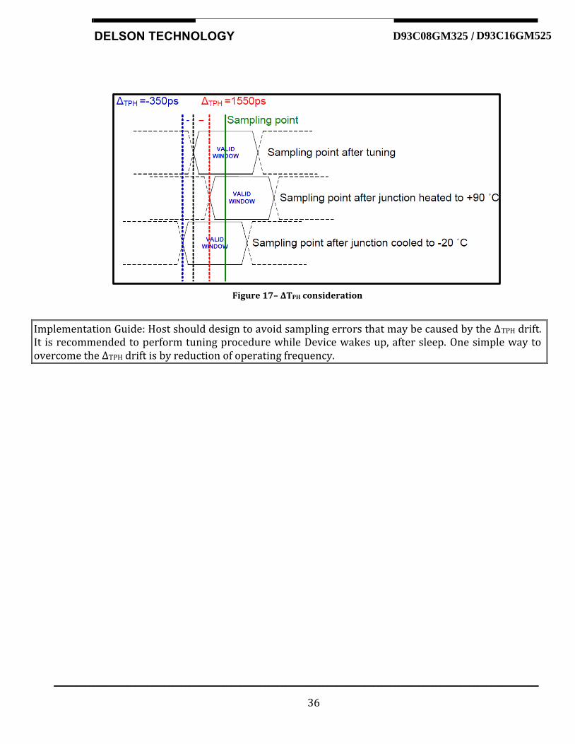
tPH parameter is defined to allow device output delay to be longer than tPERIOD. After initialization, the tPH may have random phase relation to the clock. The Host is responsible to find the optimal sampling point for the Device outputs, while switching to the HS200 mode. Figure 16 and Table 20 define Device output timing. While setting the sampling point of data, a long term drift, which mainly depends on temperature drift, should be considered. The temperature drift is expressed by ΔTPH. Output valid data window (tVW) is available regardless of the drift (ΔTPH) but position of data window varies by the drift, as described in Figure 17.
Figure 16 – HS200 Device Output Timing
Note: VOH denotes VOH(min.) and VOL denotes VOL(max.).
Table 20– Output Timing
Symbol Min. Max. Unit Remark
tPH 0 2 UI Device output momentary phase from CLK input to CMD or DAT lines output. Does not include a long term temperature drift.
ΔTPH -350
(ΔT=-20°C) +1550
(ΔT=90°C) ps
Delay variation due to temperature change after tuning. Total allowable shift of output valid window (TVW) from last system Tuning procedure ΔTPH is 2600ps for ΔT from -25°C to 125°C during operation.
TVW 0.575 - UI tVW=2.88ns at 200MHz Using test circuit in Figure 15 including skew among CMD and DAT lines created by the Device. Host path may add Signal Integrity induced noise, skews, etc. Expected TVW at Host input is larger than 0.475UI.
Note:Unit Interval (UI) is one bit nominal time. For example, UI=5ns at 200MHz.
Internet
Data
Sheet DELSON TECHNOLOGY D93C08GM325 D93C16GM525 /
____________________________________________________________________________________________________________________
36
e•MMC™ 4.5
Flash Storage Specification
e•MMC™ 4.5
Figure 17– ΔTPH consideration
Implementation Guide: Host should design to avoid sampling errors that may be caused by the ΔTPH drift. It is recommended to perform tuning procedure while Device wakes up, after sleep. One simple way to overcome the ΔTPH drift is by reduction of operating frequency.
Internet
Data
Sheet DELSON TECHNOLOGY D93C08GM325 D93C16GM525 /
____________________________________________________________________________________________________________________
37
Flash Storage Specification
e•MMC™ 4.5 6.7 Bus Timing Specification in HS400 mode
6.7.1 HS400 Device Input Timing
The CMD input timing for HS400 mode is the same as CMD input timing for HS200 mode. Figure 18 and Table 21 show Device input timing
Figure 18 - HS400 Device Data input timing
Table 21- HS400 Device input timing
Parameter Symbol Min Max Unit Remark
Input CLK
Cycle time data
transfer mode
tPERIOD 5 200MHz(Max), between rising edges With respect to VT.
Slew rate SR 1.125 V/ns With respect to VIH/VIL.
Duty cycle
distortion
tCKDCD 0.0 0.3 ns Allowable deviation from an ideal 50% duty cycle.
With respect to VT. Includes jitter, phase noise
Minimum pulse width
tCKMPW 2.2 ns With respect to VT.
Input DAT (referenced to CLK)
Input set-up time tISUddr 0.4 ns CDevice ≤ 6pF With respect to VIH/VIL.
Input hold time tIHddr 0.4 ns CDevice ≤ 6pF With respect to VIH/VIL.
Slew rate SR 1.125 V/ns With respect to VIH/VIL.
Internet
Data
Sheet DELSON TECHNOLOGY D93C08GM325 D93C16GM525 /
____________________________________________________________________________________________________________________
38
e•MMC™ 4.5 6.7.2 HS400 Device Output Timing
The Data Strobe is used to read data in HS400 mode. The Data Strobe is toggled only during data read or CRC status response.
Figure 19- HS400 Device output timing
Table 22 – HS400 Device Output timing
Parameter Symbol Min Max Unit Remark
Data Strobe
Cycle time data transfer mode tPERIOD 5 200MHz(Max), between rising edges With respect to VT
Slew rate SR 1.125 V/ns With respect to VOH/VOL and HS400 reference load
Duty cycle distortion tDSDCD 0.0 0.2 ns Allowable deviation from the input CLK duty cycle distortion (tCKDCD) With respect to VT Includes jitter, phase noise
Minimum pulse width tDSMPW 2.0 ns With respect to VT
Read pre-amble tRPRE 0.4 - tPERIOD Max value is specified by manufacturer. Value up to infinite is valid
Read post-amble tRPST 0.4 - tPERIOD Max value is specified by manufacturer.
Value up to infinite is valid
Output DAT (referenced to Data Strobe)
Output skew tRQ 0.4 ns With respect to VOH/VOL and HS400 reference load
Output hold skew tRQH 0.4 ns With respect to VOH/VOL and HS400 reference load.
Slew rate SR 1.125 V/ns With respect to VOH/VOL and HS400 reference load
NOTE 1 : Measured with HS400 reference load(6.2.4)
Internet
Data
Sheet DELSON TECHNOLOGY D93C08GM325 D93C16GM525 /
____________________________________________________________________________________________________________________
39
Flash Storage Specification
e•MMC™ 4.5 Table 23 – HS400 Capacitance
Parameter Symbol Min Type Max Unit Remark
Pull-up resistance for CMD RCMD 4.7 100(1) Kohm
Pull-up resistance for DAT0-7 RDAT 10 100(1) Kohm
Pull-down resistance for Data Strobe
RDS 10 100(1) Kohm
Internal pull up resistance DAT1-DAT7
Rint 10 150 Kohm
Single Device capacitance CDevice 6 pF
Internet
Data
Sheet DELSON TECHNOLOGY D93C08GM325 D93C16GM525 /
____________________________________________________________________________________________________________________
40
Flash Storage Specification
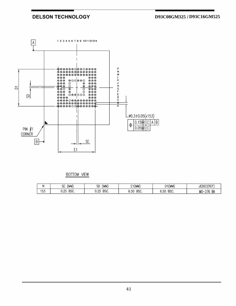
e•MMC™ 4.5 7. Package connections
Package Mechanical (11.5 x 13.0 x 1.0mm)
11.5 ± 0.1 mm
13
± 0
.1 m
m
1.0mm Max
Max 0.92mm
Min 0.15mm
0.5 BSC. (mm)
Internet
Data
Sheet DELSON TECHNOLOGY D93C08GM325 D93C16GM525 /
____________________________________________________________________________________________________________________
41
e•MMC™ 4.5
Flash Storage Specification
e•MMC™ 4.5
Internet
Data
Sheet DELSON TECHNOLOGY D93C08GM325 D93C16GM525 /
____________________________________________________________________________________________________________________
42
Flash Storage Specification
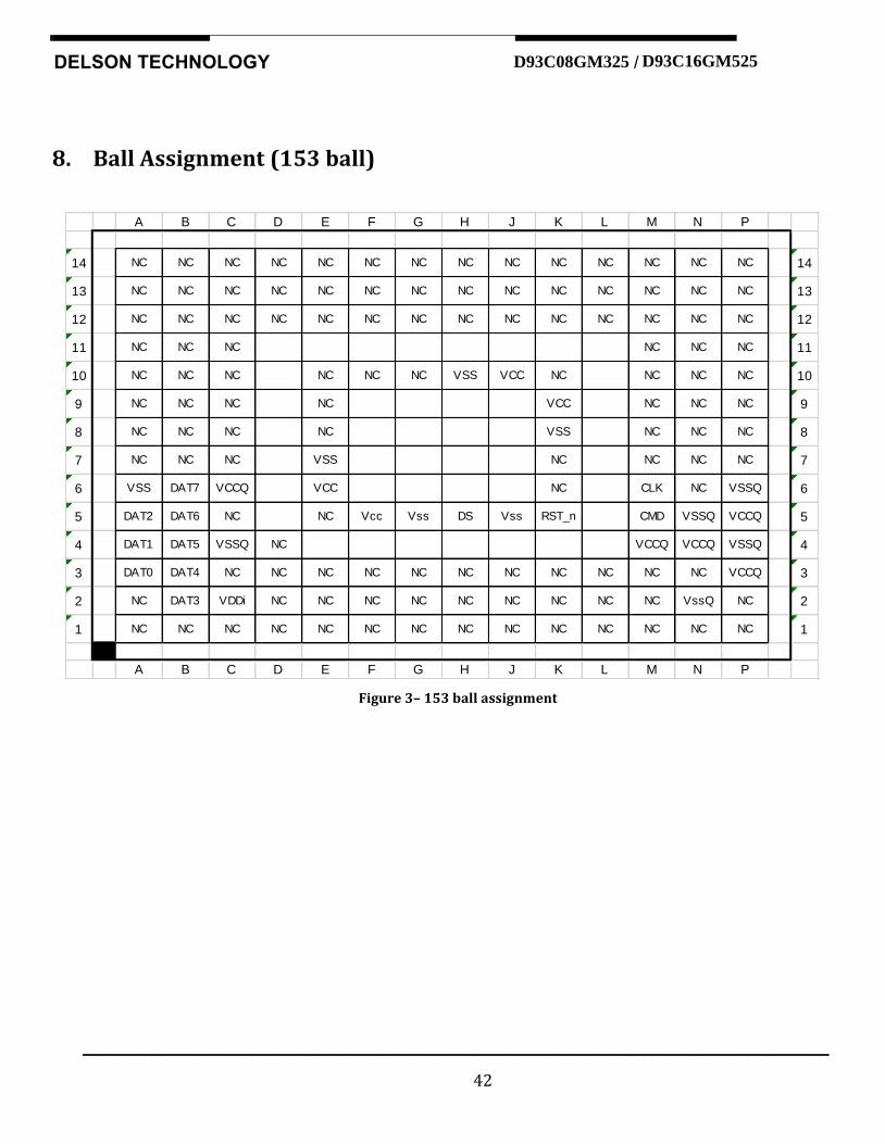
e•MMC™ 4.5 8. Ball Assignment (153 ball)
Figure 3– 153 ball assignment
A B C D E F G H J K L M N P
14 NC NC NC NC NC NC NC NC NC NC NC NC NC NC 14
13 NC NC NC NC NC NC NC NC NC NC NC NC NC NC 13
12 NC NC NC NC NC NC NC NC NC NC NC NC NC NC 12
11 NC NC NC NC NC NC 11
10 NC NC NC NC NC NC VSS VCC NC NC NC NC 10
9 NC NC NC NC VCC NC NC NC 9
8 NC NC NC NC VSS NC NC NC 8
7 NC NC NC VSS NC NC NC NC 7
6 VSS DAT7 VCCQ VCC NC CLK NC VSSQ 6
5 DAT2 DAT6 NC NC Vcc Vss DS Vss RST_n CMD VSSQ VCCQ 5
4 DAT1 DAT5 VSSQ NC VCCQ VCCQ VSSQ 4
3 DAT0 DAT4 NC NC NC NC NC NC NC NC NC NC NC VCCQ 3
2 NC DAT3 VDDi NC NC NC NC NC NC NC NC NC VssQ NC 2
1 NC NC NC NC NC NC NC NC NC NC NC NC NC NC 1
A B C D E F G H J K L M N P
Internet
Data
Sheet DELSON TECHNOLOGY D93C08GM325 D93C16GM525 /
____________________________________________________________________________________________________________________
43
Flash Storage Specification
e•MMC™ 4.5 9. Temperature
Parameter Rating Unit Note
Operating temperature -25 ~ +85 ℃
Storage temperature -55 ~ +125 ℃
Internet
Data
Sheet DELSON TECHNOLOGY D93C08GM325 D93C16GM525 /
____________________________________________________________________________________________________________________
44
Flash Storage Specification
e•MMC™ 4.5 10. Revision History Rev. History Date Remark Editor 1.0 Preliminary Nov. / 2015 2.0 Revised power consumption notes Nov. /2015
Internet
Data
Sheet DELSON TECHNOLOGY D93C08GM325 D93C16GM525 /
____________________________________________________________________________________________________________________
45
Flash Storage Specification
e•MMC™ 4.5
Appendix
Internet
Data
Sheet DELSON TECHNOLOGY D93C08GM325 D93C16GM525 /
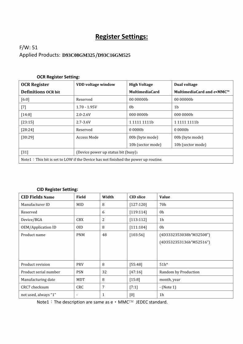
Register Settings:
F/W: 51
Applied Products: /
OCR Register Setting:
OCR Register
Definitions OCR bit
VDD voltage window High Voltage
MultimediaCard
Dual voltage
MultimediaCard and e•MMC™
[6:0] Reserved 00 00000b 00 00000b
[7] 1.70 - 1.95V 0b 1b
[14:8] 2.0-2.6V 000 0000b 000 0000b
[23:15] 2.7-3.6V 1 1111 1111b 1 1111 1111b
[28:24] Reserved 0 0000b 0 0000b
[30:29] Access Mode 00b (byte mode)
10b (sector mode)
00b (byte mode)
10b (sector mode)
[31] (Device power up status bit (busy)1
Note1:This bit is set to LOW if the Device has not finished the power up routine.
CID Register Setting:
CID Fields Name Field Width CID slice Value
Manufacturer ID MID 8 [127:120] 70h
Reserved 6 [119:114] 0h
Device/BGA CBX 2 [113:112] 1h
OEM/Application ID OID 8 [111:104] 0h
Product name PNM 48 [103:56] (4D3332353038h“M32508”)
(4D3532353136h“M52516”)
Product revision PRV 8 [55:48] 51h*
Product serial number PSN 32 [47:16] Random by Production
Manufacturing date MDT 8 [15:8] month, year
CRC7 checksum CRC 7 [7:1] - (Note 1)
not used, always “1” - 1 [0] 1h
Note1:The description are same as e•MMC™ JEDEC standard.
D93C08GM325 D93C16GM525

CSD Register Setting:
Name Field Width CSD-slice Value
CSD structure CSD_STRUCTURE 2 [127:126] 3h
System specification version SPEC_VERS 4 [125:122] 4h
Reserved - 2 [121:120] 0h
Data read access-time 1 TAAC 8 [119:112] 4Fh
Data read access-time 2 in CLK
cycles (NSAC*100)
NSAC 8 [111:104] 1h
Max. bus clock frequency TRAN_SPEED 8 [103:96] 32h
Device command classes CCC 12 [95:84] F5h
Max. read data block length READ_BL_LEN 4 [83:80] 9h
Partial blocks for read allowed READ_BL_PARTIAL 1 [79:79] 0h
Write block misalignment WRITE_BLK_MISALIGN 1 [78:78] 0h
Read block misalignment READ_BLK_MISALIGN 1 [77:77] 0h
DSR implemented DSR_IMP 1 [76:76] 0h
Reserved - 2 [75:74] 0h
Device size C_SIZE 12 [73:62] FFFh
Max. read current @ VDD min VDD_R_CURR_MIN 3 [61:59] 7h
Max. read current @ VDD max VDD_R_CURR_MAX 3 [58:56] 7h
Max. write current @ VDD min VDD_W_CURR_MIN 3 [55:53] 7h
Max. write current @ VDD max VDD_W_CURR_MAX 3 [52:50] 7h
Device size multiplier C_SIZE_MULT 3 [49:47] 7h
Erase group size ERASE_GRP_SIZE 5 [46:42] 1Fh
Erase group size multiplier ERASE_GRP_MULT 5 [41:37] 1Fh
Write protect group size WP_GRP_SIZE 5 [36:32] 0Fh-
8/
Write protect group enable WP_GRP_ENABLE 1 [31:31] 1h
Manufacturer default ECC DEFAULT_ECC 2 [30:29] 0h
Write speed factor R2W_FACTOR 3 [28:26] 2h
Max. write data block length WRITE_BL_LEN 4 [25:22] 9
Partial blocks for write allowed WRITE_BL_PARTIAL 1 [21:21] 0h
Reserved - 4 [20:17] 0h
16 GB
Content protection application CONTENT_PROT_APP 1 [16:16] 0h
File format group FILE_FORMAT_GRP 1 [15:15] 0h
Copy flag (OTP) COPY 1 [14:14] 0h
Permanent write protection PERM_WRITE_PROTECT 1 [13:13] 0h
Temporary write protection TMP_WRITE_PROTECT 1 [12:12] 0h
File format FILE_FORMAT 2 [11:10] 0h
ECC code ECC 2 [9:8] 0h
CRC CRC 7 [7:1] 30h-
8/16
Not used, always’1’ - 1 [0:0] 1h
Extended CSD Register:
Name Field Size (Bytes) CSD-slice Value
Properties Segment
Reserved1 – 6 [511:506] 0h
Extended Security
Commands Error
EXT_SECURITY_ERR 1 [505] 0h
Supported Command Sets S_CMD_SET 1 [504] 1h
HPI features HPI_FEATURES 1 [503] 1h
Background operations
support
BKOPS_SUPPORT 1 [502] 1h
Max packed read commands MAX_PACKED_READS 1 [501] 0Ch
Max packed write
commands
MAX_PACKED_WRITES 1 [500] 3Ch
Data Tag Support DATA_TAG_SUPPORT 1 [499] 1h
Tag Unit Size TAG_UNIT_SIZE 1 [498] 3h
Tag Resources Size TAG_RES_SIZE 1 [497] 0h
Context management
capabilities
CONTEXT_CAPABILITIES 1 [496] 5h
Large Unit size LARGE_UNIT_SIZE_M1 1 [495] 07h-8/16GB
Extended partitions
attribute support
EXT_SUPPORT 1 [494] 3h
Supported modes SUPPORTED_MODES 1 [493] 01h
FFU features FFU_FEATURES 1 [492] 0h
Operation codes timeout OPERATION_CODE_TIME_O 1 [491] 0h
GB
UT
FFU Argument FFU_ARG 4 [490:487] 65535
Barrier support BARRIER_SUPPORT 1 [486:486] 1h
Reserved Reserved 177 [485:309] -
CMD Queuing Support CMQ_SUPPORT 1 [308:308] 1h
CMD Queuing Depth CMQ_DEPTH 1 [307:307] 1Fh
Reserved Reserved 1 [306:306] -
Number of FW sectors
correctly programmed
NUMBER_OF_FW_SECTORS_
CORRECTLY_PROGRAMMED
4 [305:302] 0h
Vendor proprietary health
report
VENDOR_PROPRIETARY_HE
ALTH_REPORT
32 [301:270] 0h
Device life time estimation
type B
DEVICE_LIFE_TIME_EST
_TYP_B
1 [269] 01h
Device life time estimation
type A
DEVICE_LIFE_TIME_EST_TY
P_A
1 [268] 01h
Pre EOL information PRE_EOL_INFO 1 [267] 01h
Optimal read size OPTIMAL_READ_SIZE 1 [266] 01h
Optimal write size OPTIMAL_WRITE_SIZE 1 [265] 08h
Optimal trim unit size OPTIMAL_TRIM_UNIT_SIZE 1 [264] 01h
Device version DEVICE_VERSION 2 [263:262] 0h
Firmware version FIRMWARE_VERSION 8 [261:254] 51*
Power class for 200MHz,
DDR at VCC=3.6V
PWR_CL_DDR_200_360 1 [253] 0h
Cache size CACHE_SIZE 4 [252:249] 1024
Generic CMD6 timeout GENERIC_CMD6_TIME 1 [248] 19h
Power off notification(long)
timeout
POWER_OFF_LONG_TIME 1 [247] FFh
Background operations
status
BKOPS_STATUS 1 [246] 0h
Number of correctly
programmed sectors
CORRECTLY_PRG_SECTORS_
NUM
4 [245:242] 0h
1st initialization time after
partitioning
INI_TIMEOUT_AP 1 [241] 64h
Cache Flushing Policy CACHE_FLUSH_POLICY 1 [240] 1h
Power class for 52MHz, DDR
at 3.6V
PWR_CL_DDR_52_360 1 [239] 0h
Power class for 52MHz, DDR PWR_CL_DDR_52_195 1 [238] 0h
at 1.95V
Power class for 200MHz at
3.6V
PWR_CL_200_360 1 [237] 0h
Power class for 200MHz, at
1.95V
PWR_CL_200_195 1 [236] 0h
Minimum Write
Performance for 8bit at
52MHz in DDR mode
MIN_PERF_DDR_W_8_52 1 [235] 0h
Minimum Read Performance
for 8bit at 52MHz in DDR
mode
MIN_PERF_DDR_R_8_52 1 [234] 0h
Reserved1 – 1 [233] –
TRIM Multiplier TRIM_MULT 1 [232] 11h -8/16 B
Secure Feature support SEC_FEATURE_SUPPORT 1 [231] 55h
Secure Erase Multiplier SEC_ERASE_MULT 1 [230] 1h
Secure TRIM Multiplier SEC_TRIM_MULT 1 [229] 1h
Boot information BOOT_INFO 1 [228] 7h
Reserved1 – 1 [227] –
Boot partition size BOOT_SIZE_MULTI 1 [226] 20h *
Access size ACC_SIZE 1 [225] 7h-8GB,16GB
High-capacity erase unit size HC_ERASE_GRP_SIZE 1 [224] 1h
High-capacity erase timeout ERASE_TIMEOUT_MULT 1 [223] 11h-8GB,16GB
Reliable write sector count REL_WR_SEC_C 1 [222] 1h
High-capacity write protect
group size
HC_WP_GRP_SIZE 1 [221] 10h
Sleep current (VCC) S_C_VCC 1 [220] 8h
Sleep current (VCCQ) S_C_VCCQ 1 [219] 8h
Production state awareness
Timeout
PRODUCTION_STATE_AWA
RENESS_TIMEOUT
1 [218] 14h
Sleep/awake timeout S_A_TIMEOUT 1 [217] 13h
Sleep Notification timout SLEEP_NOTIFICATION_TIM
E
1 [216] 0Fh
Sector Count SEC_COUNT 4 [215:212] 00E90000-08GB*
01D20000-16GB*
Reserved (note1) – 1 [211] –
Minimum Write
Performance for 8bit at
52MHz
MIN_PERF_W_8_52 1 [210] 8h
Minimum Read Performance
for 8bit at 52MHz
MIN_PERF_R_8_52 1 [209] 8h
Minimum Write
Performance for 8bit at
26MHz, for 4bit at 52MHz
MIN_PERF_W_8_26_4_52 1 [208] 8h
Minimum Read Performance
for 8bit at 26MHz, for 4bit at
52MHz
MIN_PERF_R_8_26_4_52 1 [207] 8h
Minimum Write
Performance for 4bit at
26MHz
MIN_PERF_W_4_26 1 [206] 8h
Minimum Read Performance
for 4bit at 26MHz
MIN_PERF_R_4_26 1 [205] 8h
Reserved1 – 1 [204] –
Power class for 26MHz at
3.6V 1 R
PWR_CL_26_360 1 [203] 0h
Power class for 52MHz at
3.6V 1 R
PWR_CL_52_360 1 [202] 0h
Power class for 26MHz at
1.95V 1 R
PWR_CL_26_195 1 [201] 0h
Power class for 52MHz at
1.95V 1 R
PWR_CL_52_195 1 [200] 0h
Partition switching timing PARTITION_SWITCH_TIME 1 [199] 3h
Out-of-interrupt busy timing OUT_OF_INTERRUPT_TIME 1 [198] 4h
I/O Driver Strength DRIVER_STRENGTH 1 [197] 1Fh
Device type CARD_TYPE 1 [196] 57h
Reserved (note1) – 1 [195] –
CSD structure version – [194] 2h
Reserved (note1) – 1 [193] –
Extended CSD revision EXT_CSD_REV 1 [192] 08h
Modes Segment
Command set CMD_SET 1 [191] 0h
Reserved (note1) – 1 [190] –
Command set revision CMD_SET_REV 1 [189] 0h
Reserved (note1) – 1 [188] –
Power class POWER_CLASS 1 [187] 0h
Reserved (note1) – 1 [186] –
High-speed interface timing HS_TIMING 1 [185] 1h (note 3)
Strobe Support STROBE_SUPPORT 1 [184] 1h
Bus width mode BUS_WIDTH 1 [183] 2h (note 4)
Reserved (note1) – 1 [182] –
Erased memory content ERASED_MEM_CONT 1 [181] 0h
Reserved (note1) – 1 [180] –
Partition configuration PARTITION_CONFIG 1 [179] 0h
Boot config protection BOOT_CONFIG_PROT 1 [178] 0h
Boot bus Conditions BOOT_BUS_CONDITIONS 1 [177] 0h
Reserved (note1) – 1 [176] –
High-density erase group
definition
ERASE_GROUP_DEF 1 [175] 0h
Boot write protection status
registers
BOOT_WP_STATUS 1 [174] 0h
Boot area write protection
register
BOOT_WP 1 [173] 0h
Reserved (note1) – 1 [172] –
User area write protection
register
USER_WP 1 [171] 0h
Reserved (note1) – 1 [170] –
FW configuration FW_CONFIG 1 [169] 0h
RPMB Size RPMB_SIZE_MULT [168] 20h *
Write reliability setting
register
WR_REL_SET [167] 1Fh
Write reliability parameter
register
WR_REL_PARAM 1 [166] 04h
Start Sanitize operation SANITIZE_START 1 [165] 0h
Manually start background
operations
BKOPS_START 1 [164] 0h
Enable background
operations handshake
BKOPS_EN 1 [163] 0h
H/W reset function RST_n_FUNCTION 1 [162] 0h
HPI management HPI_MGMT 1 [161] 0h
Partitioning Support PARTITIONING_SUPPORT 1 [160] 7h
Max Enhanced Area Size MAX_ENH_SIZE_MULT 3 [159:157] 466-8GB
932-16GB
Partitions attribute PARTITIONS_ATTRIBUTE 1 [156] 0h
Partitioning Setting PARTITION_SETTING_
COMPLETED
1 [155] 0h
General Purpose Partition
Size
GP_SIZE_MULT 4 3 [154:152] 0h
General Purpose Partition
Size
GP_SIZE_MULT3 3 [151:149] 0h
General Purpose Partition
Size
GP_SIZE_MULT2 3 [148:146] 0h
General Purpose Partition
Size
GP_SIZE_MULT1 3 [145:143] 0h
Enhanced User Data Area
Size
ENH_SIZE_MULT 3 [142:140] 0h
Enhanced User Data Start
Address
ENH_START_ADDR 4 [139:136] 0h
Reserved (note1) – 1 [135] –
Bad Block Management
mode
SEC_BAD_BLK_MGMNT 1 [134] 0h
Reserved (note1) – 1 [133] –
Package Case Temperature
is controlled
TCASE_SUPPORT 1 [132] 0h
Periodic Wake-up PERIODIC_WAKEUP 1 [131] 0h
Program CID/CSD in DDR
mode support
PROGRAM_CID_CSD_DDR_S
UPPORT
1 [130] 1h
Reserved (note1) – 2 [129:128] –
Vendor Specific Fields VENDOR_SPECIFIC_FIELD 64 [127:64] –
Native sector size NATIVE_SECTOR_SIZE 1 [63] 0h
Sector size emulation USE_NATIVE_SECTOR 1 [62] 0h
Sector size DATA_SECTOR_SIZE 1 [61] 0h
1st initialization after
disabling sector size
emulation
INI_TIMEOUT_EMU 1 [60] 0h
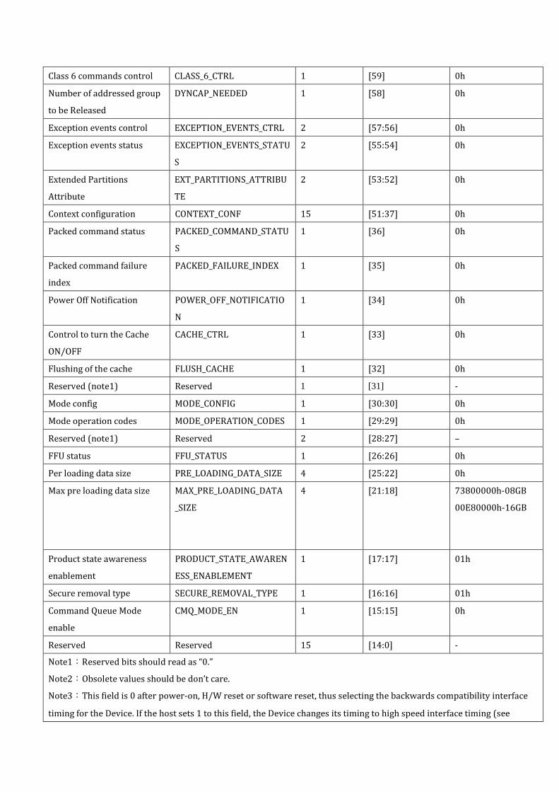
Class 6 commands control CLASS_6_CTRL 1 [59] 0h
Number of addressed group
to be Released
DYNCAP_NEEDED 1 [58] 0h
Exception events control EXCEPTION_EVENTS_CTRL 2 [57:56] 0h
Exception events status EXCEPTION_EVENTS_STATU
S
2 [55:54] 0h
Extended Partitions
Attribute
EXT_PARTITIONS_ATTRIBU
TE
2 [53:52] 0h
Context configuration CONTEXT_CONF 15 [51:37] 0h
Packed command status PACKED_COMMAND_STATU
S
1 [36] 0h
Packed command failure
index
PACKED_FAILURE_INDEX 1 [35] 0h
Power Off Notification POWER_OFF_NOTIFICATIO
N
1 [34] 0h
Control to turn the Cache
ON/OFF
CACHE_CTRL 1 [33] 0h
Flushing of the cache FLUSH_CACHE 1 [32] 0h
Reserved (note1) Reserved 1 [31] -
Mode config MODE_CONFIG 1 [30:30] 0h
Mode operation codes MODE_OPERATION_CODES 1 [29:29] 0h
Reserved (note1) Reserved 2 [28:27] –
FFU status FFU_STATUS 1 [26:26] 0h
Per loading data size PRE_LOADING_DATA_SIZE 4 [25:22] 0h
Max pre loading data size MAX_PRE_LOADING_DATA
_SIZE
4 [21:18] 73800000h-08GB
00E80000h-16GB
Product state awareness
enablement
PRODUCT_STATE_AWAREN
ESS_ENABLEMENT
1 [17:17] 01h
Secure removal type SECURE_REMOVAL_TYPE 1 [16:16] 01h
Command Queue Mode
enable
CMQ_MODE_EN 1 [15:15] 0h
Reserved Reserved 15 [14:0] -
Note1:Reserved bits should read as “0.”
Note2:Obsolete values should be don’t care.
Note3:This field is 0 after power-on, H/W reset or software reset, thus selecting the backwards compatibility interface
timing for the Device. If the host sets 1 to this field, the Device changes its timing to high speed interface timing (see

Section 10.6.1 of JESD84-B51). If the host sets value 2 the Device changes its timing to HS200 interface timing (see Section
10.8.1 of JESD84-B51), If the host sets HS_TIMING[3:0] to 0x3,the device changes its timing to HS400 interface timing
(see10.10).
Note4:It is set to ‘0’ (1 bit data bus) after power up and can be changed by a SWITCH command.
Note5: * Changed by Firmware release note