e ects of strain on the band structure of group-iii...
TRANSCRIPT

Effects of strain on the band structure of group-III nitrides
Qimin Yan,1,2 Patrick Rinke,3 Anderson Janotti,1 Matthias Scheffler,1,3 Chris G. Van de Walle1
1Materials Department, University of California, Santa Barbara, California 93106-5050, USA2Molecular Foundry, Lawrence Berkeley National Laboratory, Berkeley, California 94720, USA3Fritz-Haber-Institut der Max-Planck-Gesellschaft, Faradayweg 4–6, D-14195 Berlin, Germany
(Dated: April 26, 2014)
We present a systematic study of strain effects on the electronic band structure of the group-III-nitrides (AlN, GaN and InN). The calculations are based on density functional theory (DFT) withband-gap-corrected approaches including hybrid functional and quasiparticle G0W0 methods. Westudy strain effects under realistic strain conditions, hydrostatic pressure and biaxial stress. Thestrain-induced modification of the band structures is found to be nonlinear; transition energies andcrystal-field splittings show a strong nonlinear behavior under biaxial stress. For the linear regimearound the experimental lattice parameters, we present a complete set of deformation potentials(acz, act, D1, D2, D3, D4, D5, D6) that allows us to predict the band positions of group-III nitridesand their alloys (InGaN and AlGaN) under realistic strain conditions. We quantify the nonlinearityof strain effects by introducing a set of bowing parameters. We apply the calculated deformationpotentials to the prediction of strain effects on transition energies and valence-band structures ofInGaN alloys and quantum wells grown on GaN, in various orientations (including c-plane, m-plane,and semipolar). The calculated band gap bowing parameters including the strain effect for c-planeInGaN agrees well with the results obtained by hybrid functional alloy calculations. For semipolarInGaN QWs grown in (2021), (3031), and (3031) orientations, our calculated deformation potentialshave provided results for polarization ratios in good agreement with the experimental observations,providing further confidence in the accuracy of our values.
PACS numbers: 71.20.Nr, 72.20.Jv, 78.20.Bh, 85.60.Bt
I. INTRODUCTION
The group-III nitride semiconductors AlN, GaN, In-N, and their alloys are already extensively used in lightemitting diodes1 and laser diodes2 from the visible spec-trum to the deep ultra-violet(UV). The electronic struc-ture of these wide-band-gap semiconductors also enableshigh-power and high-frequency devices.3 However, theapplication of nitride semiconductors are currently stilllimited by several factors. For solid-state lighting, oneof the most serious limitations is the droop problem,which is believed to be related to the Auger recombi-nation process.4–6 In addition, in traditional c-plane (po-lar) quantum wells (QWs) the electron and hole wave-functions are separated by polarization fields, which low-ers the radiative recombination rate. To overcome thisproblem, and allow wider QWs that would also mitigateAuger losses, semipolar and nonpolar InGaN/GaN QWshave been proposed, where the polarization fields can begreatly reduced or even eliminated.7 Several experimen-tal groups have reported nitride-based light emitting de-vices grown on these nonpolar and semipolar planes.8–12
One effect of forming an interface between dissimilarnitride materials is the development of strain. The ac-tive regions in nitride-based light emitting devices con-sist of heterostructures such as InGaN/GaN (in light-emitting devices) or AlGaN/GaN (in power electronicdevices) MQW structures. Due to the large lattice mis-match (2.5% between AlN and GaN and 11.0% betweenInN and GaN), strain is present in alloy layers that arepseudomorphically grown on thick GaN layers or sub-strates. Strain affects the device properties in several
ways: (a) It changes the absolute positions of the valence-band maximum (VBM) and the conduction-band mini-mum (CBM), and hence modifies the QW depth and theconfinement of electrons and holes in the active region.(b) It induces piezoelectric polarization in InGaN or Al-GaN QWs,7,13,14 thus lowering the electron-hole overlapand hence the radiative recombination rate. (c) It mayalso modify the effective masses of carriers and the densi-ty of states.15,16 (d) In polar (c-plane) QWs, the in-planestrain is isotropic.17–19 In nonpolar and semipolar QWs,on the other hand, the biaxial stress induces anisotropicstrain, which drastically modifies the subband structuresand wavefunction character20–22 and induces polarizedlight emission.11,12,14
The effects of strain on the band structures of semicon-ductors can, to first order, be described by deformationpotentials. These are the linear coefficients in the re-sponse of the band structure to a strain perturbation.The applicability of such a description has been demon-stratedin measurements of the optical transition energiesfor GaN epilayers with residual strain.23–25 To quantifythe strain effects for InGaN or AlGaN alloys, accurate de-formation potential parameters for all three nitrides areneeded.
So far, most of the experimental data on deformationpotentials of GaN25–28 and InN28 have been obtained bya combination of x-ray and optical measurements fromthe change of optical transition energies under the bi-axial stress induced by the c-plane substrate. However,the accurate determination of deformation potentials bythis experimental approach is difficult. Indeed, as shownin Table I, the experimental deformation potential da-
2
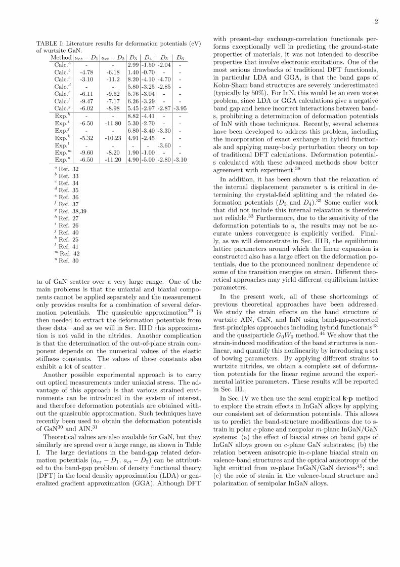
TABLE I: Literature results for deformation potentials (eV)of wurtzite GaN.
Method acz −D1 act −D2 D3 D4 D5 D6
Calc.a - - 2.99 -1.50 -2.04 -Calc.b -4.78 -6.18 1.40 -0.70 - -Calc.c -3.10 -11.2 8.20 -4.10 -4.70 -Calc.d - - 5.80 -3.25 -2.85 -Calc.e -6.11 -9.62 5.76 -3.04 - -Calc.f -9.47 -7.17 6.26 -3.29 - -Calc.g -6.02 -8.98 5.45 -2.97 -2.87 -3.95
Exp.h - - 8.82 -4.41 - -Exp.i -6.50 -11.80 5.30 -2.70 - -Exp.j - - 6.80 -3.40 -3.30 -Exp.k -5.32 -10.23 4.91 -2.45 - -Exp.l - - - - -3.60 -Exp.m -9.60 -8.20 1.90 -1.00 - -Exp.n -6.50 -11.20 4.90 -5.00 -2.80 -3.10a Ref. 32b Ref. 33c Ref. 34d Ref. 35e Ref. 36f Ref. 37g Ref. 38,39h Ref. 27i Ref. 26j Ref. 40k Ref. 25l Ref. 41m Ref. 42n Ref. 30
ta of GaN scatter over a very large range. One of themain problems is that the uniaxial and biaxial compo-nents cannot be applied separately and the measurementonly provides results for a combination of several defor-mation potentials. The quasicubic approximation29 isthen needed to extract the deformation potentials fromthese data—and as we will in Sec. III D this approxima-tion is not valid in the nitrides. Another complicationis that the determination of the out-of-plane strain com-ponent depends on the numerical values of the elasticstiffness constants. The values of these constants alsoexhibit a lot of scatter .
Another possible experimental approach is to carryout optical measurements under uniaxial stress. The ad-vantage of this approach is that various strained envi-ronments can be introduced in the system of interest,and therefore deformation potentials are obtained with-out the quasicubic approximation. Such techniques haverecently been used to obtain the deformation potentialsof GaN30 and AlN.31
Theoretical values are also available for GaN, but theysimilarly are spread over a large range, as shown in TableI. The large deviations in the band-gap related defor-mation potentials (acz −D1, act −D2) can be attribut-ed to the band-gap problem of density functional theory(DFT) in the local density approximation (LDA) or gen-eralized gradient approximation (GGA). Although DFT
with present-day exchange-correlation functionals per-forms exceptionally well in predicting the ground-stateproperties of materials, it was not intended to describeproperties that involve electronic excitations. One of themost serious drawbacks of traditional DFT functionals,in particular LDA and GGA, is that the band gaps ofKohn-Sham band structures are severely underestimated(typically by 50%). For InN, this would be an even worseproblem, since LDA or GGA calculations give a negativeband gap and hence incorrect interactions between band-s, prohibiting a determination of deformation potentialsof InN with those techniques. Recently, several schemeshave been developed to address this problem, includingthe incorporation of exact exchange in hybrid function-als and applying many-body perturbation theory on topof traditional DFT calculations. Deformation potential-s calculated with these advanced methods show betteragreement with experiment.38
In addition, it has been shown that the relaxation ofthe internal displacement parameter u is critical in de-termining the crystal-field splitting and the related de-formation potentials (D3 and D4).35 Some earlier workthat did not include this internal relaxation is thereforenot reliable.33 Furthermore, due to the sensitivity of thedeformation potentials to u, the results may not be ac-curate unless convergence is explicitly verified. Final-ly, as we will demonstrate in Sec. III B, the equilibriumlattice parameters around which the linear expansion isconstructed also has a large effect on the deformation po-tentials, due to the pronounced nonlinear dependence ofsome of the transition energies on strain. Different theo-retical approaches may yield different equilibrium latticeparameters.
In the present work, all of these shortcomings ofprevious theoretical approaches have been addressed.We study the strain effects on the band structure ofwurtzite AlN, GaN, and InN using band-gap-correctedfirst-principles approaches including hybrid functionals43
and the quasiparticle G0W0 method.44 We show that thestrain-induced modification of the band structures is non-linear, and quantify this nonlinearity by introducing a setof bowing parameters. By applying different strains towurtzite nitrides, we obtain a complete set of deforma-tion potentials for the linear regime around the experi-mental lattice parameters. These results will be reportedin Sec. III.
In Sec. IV we then use the semi-empirical k·p methodto explore the strain effects in InGaN alloys by applyingour consistent set of deformation potentials. This allowsus to predict the band-structure modifications due to s-train in polar c-plane and nonpolar m-plane InGaN/GaNsystems: (a) the effect of biaxial stress on band gaps ofInGaN alloys grown on c-plane GaN substrates; (b) therelation between anisotropic in-c-plane biaxial strain onvalence-band structures and the optical anisotropy of thelight emitted from m-plane InGaN/GaN devices45; and(c) the role of strain in the valence-band structure andpolarization of semipolar InGaN alloys.

3
II. MODEL AND COMPUTATIONAL DETAILS
A. k·p perturbation approach
We employ the k · p perturbation approach of Birand Pikus29 to obtain the analytical solutions of strain-induced band-structure modifications in the vicinity ofthe Γ point. These solutions are then used to fit the first-principles band structures to extract the deformation-potential parameters. The strained Hamiltonian of thetopmost three valence bands is given by the following6×6 matrix:
H =
F 0 −H∗ 0 K∗ 00 G ∆ −H∗ 0 K∗
−H ∆ λ 0 I∗ 00 −H 0 λ ∆ I∗
K 0 I ∆ G 00 K 0 I 0 F
, (1)
where
F = ∆1 + ∆2 + λ+ θ,G = ∆1 −∆2 + λ+ θ,H = i(A6kzk+ +A7k+ +D6εz+),I = i(A6kzk+ −A7k+ +D6εz+),K = A5k
2+ +D5ε+,
∆ =√
2∆2,λ = A1k
2z +A2k
2⊥ +D1εzz +D2(εxx + εyy),
θ = A3k2z +A4k
2⊥ +D3εzz +D4(εxx + εyy),
ε+ = εxx − εyy + 2iεxy, εz+ = εxz + iεyz,k+ = kx + iky, k
2⊥ = k2
x + k2y.
Here kx, ky, and kz are the electron wave vectors alongx, y, and z directions. εxx, εyy, and εzz are the straincomponents along x, y, and z directions respectively. εxzand εyz are shear-strain components in xz and yz planes.∆1 is the crystal-field interaction and ∆2 is the spin-orbitinteraction. Note that the element H in this Hamiltoni-an is different in sign and by a factor i from that in theapproach of Chuang and Chang.33 However, these dif-ferences do not produce any observable physical effect;previous work has shown that the same band structure isobtained from both approaches.46 We have also checkedthat such a difference in the Hamiltonian does not af-fect the dependence of the band energies at the Γ pointon the strain components, which is used to extract thedeformation potentials. Therefore, the Chuang-Chang33
and Bir-Pikus29 approaches are equivalent.For an unstrained wurtzite system, the top three va-
lence bands correspond to the heavy hole (HH), light hole(LH), and crystal-field split-off band (CH). The transi-tion energies from the CBM to these three bands aredenoted EA, EB , and EC , respectively. Here we do notconsider the spin-orbit interaction (∆2 = 0), which isvery small in the nitrides.47 In this case the HH and LHband become doubly degenerate (Γ6) in the absence of s-train and the CH band (Γ1) is split off by the crystal-fieldsplitting.
We first focus on those strain components that do notbreak the wurtzite symmetry, including biaxial strain inthe c plane (εxx = εyy) and uniaxial strain along the caxis (εzz). Such strain perturbations to the 6 × 6 k ·pHamiltonian do not split HH and LH bands, althoughthey induce an energy shift of the conduction and thethree valence bands at the Γ point:
∆ECB = aczεzz + actε⊥,∆EHH/LH = (D1 +D3)εzz + (D2 +D4)ε⊥,∆ECH = D1εzz +D2ε⊥,
(2)
yielding the following transition energies:
EA/B = EA/B(0) + (acz −D1)εzz + (act −D2)ε⊥−(D3εzz +D4ε⊥),
EC = EC(0) + (acz −D1)εzz + (act −D2)ε⊥.(3)
Here ε⊥ (defined as εxx + εyy) and εzz are the s-train components in and out of the c plane. EA/B(0)and EC(0) are the corresponding transition energies atequilibrium lattice constants. From the slopes of thetransition energies under biaxial strain in the c plane(εxx = εyy 6= 0, εzz = 0) we obtain the deformation po-tentials act − D2 and D4, while acz − D1 and D3 canbe obtained from the slope of transition energies underuniaxial strain along the c-axis (εxx = εyy = 0, εzz 6= 0).
The strain components mentioned above preserve thesymmetry of the wurtzite crystal. The hexagonal sym-metry can be broken by anisotropic strain in the c plane,which is present in nonpolar and semipolar nitride al-loys. For example, uniaxial strain in the c plane (εyy =εzz = 0, εxx 6= 0) changes the crystal symmetry from C6v
to C2v. Without spin-orbit splitting, the original 6 × 6Hamiltonian reduces to a 3×3 matrix. Anisotropic strainin the c plane lifts the degeneracy of the Γ6 states andyields the three eigenenergies:
E1 = EA/B(0) + (D2 +D4)εxx +D5εxx,E2 = EA/B(0) + (D2 +D4)εxx −D5εxx,E3 = EC(0) +D2εxx.
(4)
Correspondingly the three eigenstates are: 110
,
−110
,
001
. (5)
The basis of the eigenvectors is:
|1〉 = |X + iY 〉 ,|2〉 = |X − iY 〉 ,|3〉 = |Z〉 ,
(6)
where the characters X/Y /Z indicate that the corre-sponding wavefunction has px/py/pz character. The firsteigenvector in Eq. (5) has px character while the secondeigenvector has py character. We obtain the magnitudeof the deformation potential D5 from the slope of the en-ergy splitting between the top two valence bands underanisotropic strain:
∆E = |EX − EY | = 2 |D5εxx| . (7)

4
FIG. 1: (Color online) Partial charge density of (a) the high-est and (b) the second highest valence band of wurtzite GaNunder compressive uniaxial strain in the c plane.
In order to decide the sign ofD5, we need to explore thesymmetry character of the valence bands. Figure 1 showsthe partial charge density of the topmost two valencebands of wurtzite GaN under uniaxial compressive strainalong the x direction. The highest valence state exhibitspx character, while the second highest state exhibits pycharacter. This implies that D5 is negative in GaN, inagreement with experimental observations.40 Based onthe calculated partial charge densities of AlN and InN(not shown here), we find that the D5 values in AlN andInN are also negative.
Another strain component that is present in semipo-lar nitride materials is shear strain (εxz and εyz). Thecorresponding deformation potential is D6. By applyingonly the shear strain εxz in the wurtzite system, neglect-ing the spin-orbit interaction, the topmost three valence-band eigenenergies at the Γ point are:
E1 = ∆cr,
E2 = ∆cr
2 +
√∆2
cr+8D26ε
2xz
2 ,
E3 = ∆cr
2 −√
∆2cr+8D2
6ε2xz
2 .
(8)
We obtain the valence-band structures of the shear-strained wurzite GaN system from first-principles cal-culations. The energy separation between E2 and E3
is defined as ∆E23 =√
∆2cr + 8D2
6ε2xz. The energy of
one of the doubly degenerate valence-bands (E1, with pycharacter) stays constant while the other one (E2, withpx character) goes up. Correspondingly, the crystal-fieldsplit-off band (E3, with pz character) goes down with thesame magnitude.
Above we have presented the definitions of all defor-mation potentials that are needed to describe the mod-ification of the band structure with strain at the Γpoint. In order to determine these deformation poten-tials from first-principles calculations, we apply differen-t strain components in the wurtzite nitride systems andthen fully relax the structure including the internal struc-tural parameter u (which sensitively affects the magni-tude of the crystal-field splitting). By fitting the analyt-ical expressions for the k·p eigenenergies at the Γ pointto the calculated band structures with different straincomponents, the deformation potentials are obtained.
B. First-principles calculations
The DFT calculations are carried out using the plane-wave projector augmented-wave (PAW)48 method asimplemented in the VASP code.49 We use the Heyd-Scuseria-Ernzerhof (HSE)43,50 hybrid functional to carryout the structural optimization as well as band-structurecalculations, which gives band gaps and equilibrium lat-tice parameters in better agreement with experiment fornitrides than LDA and GGA, as shown in our previouswork.38 The screening parameter µ in HSE is fixed at avalue of 0.2. With the default mixing parameter (25%),the obtained band gap of InN (0.68 eV) agrees prettywell with experiment ( 0.7 eV). For AlN and GaN, themixing parameter α is modified (34% for AlN, 30% forGaN) to reproduce the experimental band gaps (6.13 eVfor AlN, 3.48 eV for GaN). We treat the semi-core d elec-trons of Ga and In as valence electrons. We use a plane-wave energy cutoff of 600 eV, which is necessary for theaccurate determination of the internal displacement pa-rameter u, and a 6×6×4 Γ-point centered k-point mesh.Our quasiparticle G0W0 calculations were based on exac-t exchange in the optimized effective potential approach(G0W0@OEPx).44
III. COMPUTATIONAL RESULTS
A. Equilibrium lattice parameters and band gaps
The lattice parameters of the wurtzite crystal structurefor AlN, GaN, and InN are shown in Table II. LDA un-derestimates the equilibrium lattice parameters of AlN,GaN, and InN, while GGA overestimates these param-eters compared with experimental data. The deviationsare on the order of 1%, which is typical of these function-als. The HSE results for structural properties with thedefault mixing parameter are typically closer to experi-ment. The HSE band structures obtained in Ref. 38 wereobtained with the default mixing parameter α = 25%.Although a better agreement with experiment comparedwith LDA or GGA was achieved, the calculated bandgaps for the three nitrides were still smaller than exper-iment. Better agreement with experimental band gapscan be achieved by modifying the mixing parameter. Themixing parameters needed to reproduce the experimen-tal band gaps of group-III nitrides at the experimentallattice parameters are 34% for AlN and 30% for GaN.As shown in Table II, the modified mixing parameter al-so provides a good agreement with experiment for thestructural properties.
The band structures of group-III nitride semiconduc-tors AlN, GaN, and InN obtained with the hybrid func-tional approach with modified mixing parameters areshown in Fig. 2. These band structures show good a-greement with results obtained with the quasiparticleG0W0@OEPx method,51 which serves as a validation ofthe use of HSE as a reliable method to obtain accurate

5
TABLE II: Equilibrium lattice parameters (a and c) and bandgaps (Eg) obtained with LDA, GGA, and HSE (with differentmixing parameter α). For the cases with modified mixing pa-rameter α, the band gaps are obtained at experimental latticeparameters. Experimental lattice parameters at T = 300 Kare taken from Refs. 51 and band gaps at low temperatureare taken from Refs. 52 and Refs. 53.
Method a (A) c (A) u Eg (eV)AlN LDA 3.092 4.950 0.3818 4.40
GGA 3.127 5.021 0.3812 4.10HSE (α=0.25) 3.102 4.971 0.3819 5.64HSE (α=0.34) 3.096 4.957 0.3820 6.13
Exp. 3.112 4.982 - 6.15GaN LDA 3.155 5.145 0.3764 2.12
GGA 3.215 5.240 0.3766 1.74HSE (α=0.25) 3.182 5.173 0.3772 3.27HSE (α=0.30) 3.174 5.162 0.3773 3.48
Exp. 3.190 5.189 - 3.51InN LDA 3.504 5.670 0.3784 < 0
GGA 3.573 5.762 0.3792 < 0HSE 3.548 5.751 0.3796 0.68Exp. 3.540 5.706 - 0.7
band structures.
B. Transition energies in GaN under realistic strain
Optical transitions from the lowest conduction band tothe topmost three valence bands are dominant for opti-cal emission processes in nitride materials. In GaN thesetransitions have also been used as a characterization toolto evaluate the effects of strain on the electronic prop-erties. In this section, we will analyze the strain de-pendence of these transition energies in c-plane GaN bycomputing the band structures of GaN for two types ofrealistic strain conditions: biaxial stress and hydrostaticpressure.
Wurtzite c-plane GaN thin films grown on sapphire orSiC experience biaxial stress induced by the substrate.Under such stress, the wurtzite system exhibits biaxialstrain in the c plane accompanied by out-of-plane strainalong the c axis:
εzz = −2C13C33
εxx, εxx = εyy 6= 0. (9)
Here we use the elastic constants C13 and C33 obtained byDFT calculations performed within the LDA54 to deter-mine the strain components and lattice parameters underbiaxial stress.
Figure 3(a) shows the transition energies between thelowest conduction band and the topmost three valencebands (HH, LH and CH) of GaN under biaxial stress inthe c plane for the strain range ±3%. Interestingly, thetransitions between the CB and HH or LH bands showa strong nonlinear behavior. Such nonlinearity is alsoevident in the crystal-field splitting (∆cr) in Fig. 3(b),which can be described by a quadratic dependence as
FIG. 2: Band structures of (a) AlN, (b) GaN, and (c) InNat the experimental lattice parameters, calculated using DFTand the HSE hybrid functional with mixing parameters α ad-justed to reproduce the experimental band gap (see text).
demonstrated by the fitted curve. This implies that theslope (which defines the deformation potentials) differsfor different lattice parameters.
Another realistic strain condition can be induced byhydrostatic pressure, where the stress components alongthree directions are the same (σxx=σyy=σzz). The in-c-plane strain and out-of-c-plane strain now have the same

6
3.12 3.16 3.20 3.24 3.28-0.2
-0.1
0.0
0.1
0.2
0.3
0.4-0.03 -0.02 -0.01 0.00 0.01 0.02 0.03
Strain
cr
(eV
)
a ( )Å3.12 3.16 3.20 3.24 3.28
2.8
3.0
3.2
3.4
3.6
-0.03 -0.02 -0.01 0.00 0.01 0.02 0.03Strain
Tra
nsi
tio
nen
erg
y(e
V) E
A
EC
a (A)
o
(a) (b)
aa a
FIG. 3: (Color online) (a) Transition energies EA and EC
of GaN under biaxial stress. (b) Crystal-field splitting ofGaN under biaxial stress calculated with the HSE approach.Symbols correspond to calculated values, solid lines representsecond-order polynomial fits. The dashed line is a linear fitaround the equilibrium lattice parameter.
(a) (b)
3.12 3.16 3.20 3.24 3.282.4
2.6
2.8
3.0
3.2
3.4
3.6
3.8
4.0
-0.03 -0.02 -0.01 0.00 0.01 0.02 0.03
EA
EC
Strain
Tra
nsi
tio
nen
erg
y(e
V)
a ( )Å
3.12 3.16 3.20 3.24 3.28
0.01
0.02
0.03
0.04
-0.03 -0.02 -0.01 0.00 0.01 0.02 0.03
Åa ( )
Strain
cr
(eV
)
a a
FIG. 4: (Color online) (a) Transition energies EA and EC ofGaN under hydrostatic pressure. (b) Crystal-field splittingof GaN under hydrostatic pressure. The data are calculat-ed using DFT and the HSE hybrid functional. Data pointscorrespond to calculated values, solid lines represent second-order polynomial fits. The dashed line is a linear fit aroundthe equilibrium lattice parameter.
sign but these strain components are not isotropic:
εzz = C11 + C12 − 2C13C33 − C13
εxx,
εxx = εyy = C33 − C13
C33(C11 + C12)− 2C213
σzz.(10)
Under hydrostatic pressure, as shown in Fig. 4, boththe transition energies and the crystal-field splittingchange almost linearly in the strain range ±3%.
C. Results for deformation potentials
We have seen that the dependence of the band ener-gies on strain in general is nonlinear. However, over a
small range of strains around a given lattice parameter,the variation can be regarded as linear. It is thereforestill possible to define a single set of deformation po-tentials, choosing the experimental lattice parameters asthe point of reference. By constraining the strain rangeto realistic strain conditions in the linear regime aroundthe experimental lattice parameters, we derive a consis-tent and complete set of deformation potentials for allthree nitrides. The resulting values are listed in Table III.The recommended values are those obtained with DFT-HSE, with the mixing parameter α adjusted to obtaina band gap that matches experiment. For comparison,for GaN and AlN, we also list results obtained with oth-er exchange-correlation functionals and with HSE usingthe standard (α=0.25) mixing parameter. For InN, LDAand GGA results are not available since these functionalsproduce a negative band gap.
Table III shows that the calculated deformation poten-tials are sensitive to the choice of exchange-correlationfunctional. LDA and GGA-PBE data agree well witheach other, but both of them show appreciable devia-tions from HSE results. The band-gap-related deforma-tion potentials acz −D1 and act −D2 obtained by HSEcalculations are considerably larger in magnitude thanthose from LDA and GGA-PBE results. The HSE cal-culations with modified mixing parameters, which yieldboth very good structural properties and band structures,are expected to also provide a reliable description of thechange of band gaps under strain. The deformation po-tentials D3, D4, D5, and D6, which relate to the split-ting of valence bands, are less sensitive to the choice ofexchange-correlation functional. With the exception ofacz−D1, the deformation potentials decrease in absolutevalue from AlN to GaN to InN.
D. Deformation potentials: validity, reliability, andcomparison with experiment
We checked the validity of the HSE hybrid function-al results by performing quasiparticle G0W0 calculation-s based on OEPx.44 The comparison (included in Ta-ble III) shows that, the deformation potentials of GaNobtained with DFT-HSE calculations are in good agree-ment with those obtained from G0W0 calculations (with-in 0.5 eV). Among these deformation potentials, acz−D1
and act − D2 are more sensitive to the gap and hencepresent the most important test. The agreement withG0W0 data for these two deformation potentials vali-dates the reliability of the HSE method in determiningdeformation potentials of nitrides and oxides.55 Althoughboth HSE and G0W0 calculations properly address theband-gap problem, here we recommend HSE, since theHSE calculations can selfconsistently provide accurateresults for both structural properties and band struc-tures. Table III also shows that results obtained fromHSE with modified mixing parameters are generally very

7
TABLE III: Deformation potentials (eV) of wurtzite AlN, GaN and InN obtained from DFT with LDA, GGA, and HSEfunctionals, and from the G0W0 quasiparticle approach. The calculated quantities are obtained at the experimental equilibriumlattice parameters. For GaN, the range of experimentally determined deformation potentials and the values recommended byVurgaftman and Meyer (Ref. 52) are also listed.
Method acz −D1 act −D2 D3 D4 D5 D6
AlN LDA -3.44 -11.39 8.97 -3.95 -3.36 -GGA -3.39 -11.38 9.12 -4.01 -3.37 -
HSE (α=0.25) -4.21 -12.07 9.22 -3.74 -3.30 -4.49HSE (α=0.34) (recommended) -4.36 -12.35 9.17 -3.72 -2.93 -4.58
GaN LDA -4.56 -8.03 5.61 -3.03 -2.94 -GGA -4.46 -8.08 5.83 -2.98 -3.13 -
HSE (α=0.25) -6.02 -8.98 5.45 -2.97 -2.87 -3.95HSE (α=0.30) (recommended) -6.07 -8.88 5.38 -2.69 -2.56 -3.88
G0W0@OEPx -5.49 -8.84 5.80 -3.10 - -Exp. range -9.6 . . . -3.1 -11.8 . . . -8.1 1.4 . . . 8.2 -4.1 . . . -0.7 -4.7 . . . -2.4 -
Vurgaftman and Meyera -4.90 -11.30 8.20 -4.10 -4.60 -InN HSE (recommended) -3.64 -4.58 2.68 -1.78 -2.07 -3.02
a Ref. 52.
close (within 0.3 eV) to the HSE results obtained with thedefault mixing parameter (25 %). For GaN and AlN, werecommend HSE data obtained with the modified mixingparameters, since this approach provides more accurateatomic and electronic structures. Table III also lists therange of experimental data for deformation potentials ofGaN, as reported in Ref. 52; we note that our HSE resultsall fall within this (very wide) range.
Our deformation potential data also allow us to assessthe accuracy of the quasicubic approximation. This ap-proximation assumes a correlation of the physical prop-erties of the wurtzite structure with those of the zinc-blende structure along the <111> direction due to thesimilarity of the local atomic bonding environment be-tween wurtzite and zinc-blende structures. In the qua-sicubic approximation, the deformation potentials arerelated as follows: D3 = −2D4, D1 + D3 = D2 andD3 + 4D5 =
√2D6. As a test, we checked the value
of D3 + 2D4 (which should be zero in the quasicubic ap-proximation), finding 1.43 eV for AlN, -0.52 for GaN and-0.88 eV for InN. Clearly, neglecting the anisotropy of thewurtzite phase by applying the quasicubic approximationintroduces significant inaccuracies in the determinationof deformation potentials.
In Table III we also list the deformation potentials sug-gested for GaN by Vurgaftman and Meyer,52 which areobtained by averaging available data. Our HSE calcula-tions for GaN yield systematically smaller absolute valuesthan the Vurgaftman and Meyer numbers, with the ex-ception of acz − D1. For InN, Vurgaftman and Meyerrecommended to use the same deformation potentials asfor GaN due to the lack of data. Our HSE values showthat the deformation potentials of InN are much smallerthan those of GaN, with differences in magnitude as largeas several eV; use of the GaN values would therefore leadto significant errors.
TABLE IV: Bowing parameters (eV) for strain effects on tran-sition energies of wurtzite AlN, GaN and InN obtained fromDFT-HSE calculations. These bowing parameters should beused in conjunction with the recommended deformation po-tentials given in Table III. All quantities are obtained at theexperimental equilibrium lattice parameters.
b1 b2 b3 b4AlN -35.21 7.76 26.96 -14.50GaN -7.02 -0.63 -6.49 -7.66InN 6.66 -1.51 -13.34 -4.94
E. Nonlinear effects on transition energies
To quantify the nonlinearities in the effect of strain ontransition energies, we introduce a set of bowing param-eters, b1 to b4. Assuming that the bowing parametersfor the strain components along the x and y directionare equal to each other, the dependence of the transitionenergies (EA/B and EC) on strain can be expressed as:
EA/B = EA/B(0) + (acz −D1)εzz + (act −D2)ε⊥−(D3εzz +D4ε⊥) + (b1 + b3)ε2
zz + (b2 + b4)ε2⊥,
EC = EC(0) + (acz −D1)εzz + (act −D2)ε⊥+b1ε
2zz + b2ε
2⊥.
(11)EA/B(0) and EC(0) denote the transition energies at ex-perimental equilibrium lattice parameters, while EA/B
and EC are the transition energies when strain is applied.We obtain the bowing parameters for GaN by performinga quadratic fit of our transition-energy-strain data shownin Fig. 3 and Fig. 4. Similar calculations were performedfor AlN and InN and the resulting bowing parameters arelisted in Table IV. This set of bowing parameters is anessential input to model the optical transitions in highlystrained nitride heterostructures.

8
IV. STRAIN EFFECTS IN INGAN ALLOYS
Now that we have a complete set of deformation poten-tials for GaN and InN, we can study the effects of strainon the band structure of InxGa1−xN alloys. InxGa1−xNlayers grown pseudomorphically on GaN are under largebiaxial stress due to the lattice mismatch. The resultingstrain strongly affects the band structure. In addition,for c-plane-grown devices the strain causes piezoelectricpolarization, which induces electron-hole separation andlowers the radiative recombination rate and hence the ef-ficiency. For this reason, growth in nonpolar and semipo-lar orientations, which avoid the polarization fields, hasbeen pursued to improve the device efficiencies.8,9,56 Insuch nonpolar and semipolar InxGa1−xN layers, strainplays a crucial role in determining the polarization char-acter of the emitted light. In this Section we explore theeffects of strain on InxGa1−xN alloys in detail.
A. Band gap of c-plane InGaN alloys
The incorporation of In into GaN lowers the bandgap and allows tuning the emission wavelength ofInxGa1−xN-based devices over a wide spectral range fromred to blue.58 InxGa1−xN epilayers grown on GaN arepseudomorphically strained, which affects the band gap.In addition, even in the absence of strain, the band-gapvariation with In concentration is nonlinear, an effectknown as band-gap bowing. For InxGa1−xN a surprising-ly wide range of bowing parameters has been reported inthe literature.17–19,57,59,60 Moreover, the bowing parame-ter was found to dependent on the In composition.57,59,61
Here we aim to obtain a more accurate value for the bow-ing parameter by using our calculated deformation poten-tials to determine the effects of strain on the gap. Theseeffects need to be subtracted from the experimental band-gap data before the effect of bowing can be determined.
It has been verified using hybrid functional calculationsthat the equilibrium lattice parameters of the InxGa1−xNalloy can be obtained by linear interpolation betweenGaN and InN: aInGaN = aInN × x + aGaN × (1 − x)(Ref. 61). Similarly, the elastic constants and defor-mation potentials of the alloy systems can be deter-mined from those of the pure nitrides by linear inter-polation: CInGaN = CInN × x + CGaN × (1 − x) andDInGaN = DInN×x+DGaN× (1−x). For these physicalquantities, treating the dependence on alloy compositionup to linear order is sufficient. Any nonlinearities wouldhave negligible effects on the relevant observables. Theband gap of a free-standing alloy is calculated using theequation: Eg = EInN×x+EGaN× (1−x) + b×x(1−x)with the bowing parameter b.
Assuming that the InxGa1−xN epilayer is pseudomor-phically strained to match the in-plane latttice constantof GaN, the in-c-plane biaxial strain components are de-termined by the lattice mismatch between InGaN andGaN: εxx = εyy = (aGaN − aInGaN)/aInGaN. The cor-
responding out-of-plane strain component is related tothe in-plane strain by a combination of elastic constantsof the alloy: εzz = − 2C13
C33εxx. In the following we use
the elastic constants calculated by Wright et al.54 Weuse Eq. (2) to calculate the strain effects on the bandgap of an InGaN alloy as a function of In compositon.In previous work17,57,59 strain effects on the band gapwere assumed to be a linear function of the In fractionx. However, as shown in Fig. 5(a), such a linear relationdoes not hold true. The nonlinearity arises because thedeformation potentials of InGaN alloys are not constant,i.e., they cannot be taken to be equal to those of GaN,but depend on the In composition. Since the differencein deformation potentials between GaN and InN is quitelarge, the changes in band positions, which are product-s of deformation potentials and strains, exhibit distinctnonlinearities.
Using this more accurate treatment of strain effects,we can now rederive the bowing parameter of unstrainedInxGa1−xN alloys by fitting the experimental data ofband gaps measured by McCluskey et al.17,57 As shown inFig. 5(b), from our calculations, the three transition ener-gies of the c-plane InGaN system decrease with increasingIn composition, while the energy separation between H-H/LH bands and the CH band increases with increasingIn composition. The band gap of an InxGa1−xN alloy as afunction of In composition is shown in Fig. 5(c), for botha free-standing (unstrained) alloy and an alloy straineddue to pseudomorphic growth on GaN. By fitting our cal-culated band gap (solid curve) to the experimental data[solid dots in Fig. 5(c)], a bowing parameter of 2.0 eVis derived for InxGa1−xN alloys within the compositionrange 0 < x < 0.1. Strictly speaking, the bowing param-eter depends on alloy composition, but the experimen-tal data set is obviously not rich enough to address thisadditional complication, and the use of a fixed bowingparameter over this relatively narrow composition rangeis justified. The value b=2.0 eV is smaller than the re-sult derived by McCluskey et al.,57 but agrees very wellwith the result obtained by recent first-principles hybridfunctional calculations.61,62
B. Strain effects on the polarization character ofnonpolar m-plane InGaN
Nonpolar InGaN/GaN QWs have been proposed andfabricated as promising candidates for high-efficiencylight emitters8,63,64 because polarization fields in such de-vices are expected to be greatly reduced, resulting in en-hanced efficiency. The lack of polarization fields, in turn,allows the use of wider QWs, which reduce the carrierdensity in the active layer for a given amount of inject-ed current. These lower carrier densities are beneficialbecause they reduce losses due to Auger recombination,a loss mechanism that scales as the third power of thecarrier density.6,65
Light emitted from nonpolar InGaN/GaN QWs has

9
0.00 0.05 0.10 0.150.00
0.02
0.04
0.06
0.08
0.10
E
(eV
)
In composition
(a) (b) (c)
0.00 0.05 0.10 0.152.8
2.9
3.0
3.1
3.2
3.3
3.4
3.5
strained
free standing
Ba
nd
ga
p(e
V)
In composition0.150.0 0.1 0.2 0.3
2.2
2.4
2.6
2.8
3.0
3.2
3.4
3.6
En
erg
y(e
V)
In composition
EA
EB
EC
FIG. 5: (Color online) (a) Calculated band-gap change purely due to strain effects in an InxGa1−xN alloy grown pseudomor-phically on c-plane GaN. (b) Calculated transition energies of InGaN alloys grown on GaN as a function of In composition. (c)Band gap of InxGa1−xN alloys with (solid line) and without (dashed line) strain effects. The bowing parameter is adjusted toprovide an optimal fit to the experimental data of Refs. 17 and 57 (shown as black dots), resulting in a value b=2.0 eV.
0.0 0.1 0.2 0.3 0.4
-0.04
-0.02
0.00
0.02
0.04
yy
zz
Str
ain
In composition
xx
0.0 0.1 0.2 0.3 0.42.2
2.4
2.6
2.8
3.0
3.2
3.4
3.6
E3
E2
E1
y
x
In Composition
Tra
nsi
tio
nen
erg
y(e
V)
z
0.0 0.1 0.2 0.3 0.40.02
0.03
0.04
0.05
0.06
0.07
In composition
En
erg
yse
pa
rati
on
(eV
)
(a) (b) (c)
In c
FIG. 6: (Color online) (a) Strain components in InxGa1−xN alloys grown pseudomorphically on m-plane GaN. (b) Transitionenergies ofm-plane InxGa1−xN alloys. (c) Energy separation between the topmost two valence bands (E1 and E3). Experimentaldata from Masui et al.14 are shown as black dots.
been found to be polarized.9,14,56,66,67 The emitted lighthas a preferential polarization along the [1120] (x) direc-tion, while the weaker transition has a polarization alongthe [0001] (z) direction (i.e., along the c axis, which liesin the plane of the active layer in these nonpolar devices).Defining the polarization ratio as ρ = (Ix− Iz)/(Ix + Iz),Masui et al.14 further found that the polarization ratio in-creases with increasing In composition, and correspond-ingly the energy separation between the valence band-s with x character and z character increases. Here weexplore how strain affects the band ordering and polar-ization characteristics of the optical transition in suchm-plane-oriented InxGa1−xN alloys.
For InxGa1−xN alloys grown on m-plane GaN sub-strates, the two principal directions in the m plane are[1120] (x) and [0001] (z), while the direction normal to
the m plane is [1100] (y). The in-m-plane strain com-ponents are determined by the lattice mismatch betweenthe InGaN alloy and the GaN substrate, while the out-of-plane strain component (along the y direction) is de-
termined by the relation: εyy = −C11C33
εxx − C12C33
εzz. As-
suming that the InGaN film is perfectly strained by theunderlying GaN without any strain relaxation, the straincomponents in the alloy are calculated from the latticemismatch and elastic constants, as shown in Fig. 6(a).The strain component along the x direction εxx is com-pressive while that along the y direction εyy is tensile.This difference between εxx and εyy (which is absentin InxGa1−xN alloys grown along the polar c direction)plays a crucial role in the modification of the band struc-ture of m-plane InxGa1−xN alloys by splitting the HH

10
and LH bands and leading to polarized light emission.With our deformation potentials and the expressions
for band energies in Eq. (4), we calculate the transitionenergies of an InxGa1−xN alloy as a function of In com-position, as shown in Fig. 6(b). The difference betweenεxx and εyy lowers the symmetry of the wurtzite sys-tem from C6v to C2v and splits the HH and CH bands.These two bands are denoted now as E1 and E2, respec-tively, since the strain perturbation breaks the originaltwo |X ± iY 〉 states into px-like and py-like states. Bysolving the strained k ·p Hamiltonian, we find that theeigenstate of the E1 band has px character while that ofthe E2 band has pz character. Furthermore, at a verylow In composition (x=0.04) the E2 valence band cross-es the CH band, which is pz-like and denoted as the E3
band. This indicates that in m-plane InxGa1−xN alloyswith In compositions higher than 4%, the band orderingnear the valence-band edge is E1, E3, and E2 in order ofdecreasing electron energy. The dominant optical transi-tion is therefore from the conduction band to the E1 bandand the emitted light from this transition has polariza-tion mainly along the x direction. The next possible butmuch weaker transition is from the CBM to the E3 band,leading to polarization along the z direction. Such a bandordering and polarization character of the emitted lightis consistent with recent experimental observations.9,14,67
As shown in Fig. 6(c), the energy separation betweenthe E1 and E3 valence bands increases with increasingIn composition. This implies that the relative hole occu-pation of the lower band decreases and the polarizationratio increases, in agreement with the experimental ob-servations of Ref. 14 at low In compositions. A discontin-uous change in the experimental data occurs around anIn composition of 0.2. This variation cannot be explainedif we assume that the alloy is perfect and fully strained bythe underlying GaN. The discrepancy is possibly due toIn segregation, or to strain relaxation in these nonpolarInxGa1−xN alloys with high In fraction.
C. The role of strain in the valence-band structureof semipolar InGaN alloys
Semipolar QW orientations have been proposed to in-crease the efficiency of light emitters. In these orienta-tions the effect of spontaneous and piezoelectric polariza-tion fields is reduced and thereby the carrier overlap isincreased.8,11,63,64 Similar to the nonpolar case, growth ofInGaN on GaN along semipolar directions leads to strainconditions different from those in conventional growth a-long the c direction. Strain in semipolar InGaN grown onGaN is characterized by the shear strain and anisotropicstrain in the c plane. This affects the splitting of the up-permost valence bands and hence the polarization of theemitted light. Optical anisotropy has been observed forsemipolar devices.11,12,45,68,69 In addition, in semipolar(1122) InGaN QWs grown on GaN the dominant polar-ization direction was found to switch from [1100] (perpen-
dicular to the c-axis) to [1123] when the In concentrationwas increased above 30%.70,71
Three factors critically influence the band structure ofInGaN QWs and therefore the polarization of the emittedlight: indium concentration, strain, and quantum con-finement. Based on k·p modeling Yamaguchi predictedthat the QW thickness strongly affects the polarization.72
This seems qualitatively consistent with the results ofMasui et al., who observed an enhancement in opticalpolarization for thinner QWs.71 However, in Yamaguchi’swork the magnitude of this quantum confinement effectis very sensitive to the choice of Luttinger parameters51
and can range from 2 to 20 meV for 2nm thick QWs. Ue-da et al., on the other hand, found no appreciable QWthickness effect.70 They proposed strain to be the domi-nant factor, and derived a large shear-strain deformationpotential of D6=-8.8 eV from their measurements.70 Ourown study of quantum confinement73 also produced verysmall differences compared to bulk calculations; the maincause of polarization switching must therefore be the s-train.
In previous work,21 we found that anisotropic strain(through the deformation potential D5) and shear strain(through the deformation potential D6) have oppositeeffects on the valence-band separation. A switch in theband ordering may occur if the shear strain and/or thedeformation potential D6 are large enough. However, us-ing our consistent set of deformation potentials we foundno evidence of any switch in band ordering with increas-ing In concentration.21 Note that the D6 value derivedby Ueda et al.70 is much larger than any of our calculatedvalues. We conclude that the underlying cause of the po-larization switching remains unresolved. One possible ex-planation is that the switching is due to inhomogeneitiesof In concentrations and strain distributions in InGaNalloys with high In content. A recent theoretical worksupports our conclusion that the polarization switchingwith increasing carrier density may be attributed to in-homogeneous strain distribution in the InGaN quantumwells.74
Polarized light emission has also been observed insemipolar InGaN QWs grown in (2021), (3031), and(3031) orientations, and in all cases our calculated de-formation potentials have provided results for polariza-tion ratios in good agreement with the experimentalobservations,11,12 providing further confidence in the ac-curacy of our values.
V. CONCLUSION
We have studied strain effects on the band structureof wurtzite AlN, GaN, and InN using a first-principlesapproach based on density functional theory with a hy-brid functional. We observed nonlinearities in the straindependence and obtained a set of strain bowing parame-ters that can be used to account for nonlinear effects onband structure in highly strained nitrides. For the lin-

11
ear regime around the experimental lattice parameters,we have presented a complete and consistent set of de-formation potentials for the three nitride materials. Ex-amples of how our deformation potentials can be used inthe interpretation of experimental data on InGaN alloysand quantum wells were provided. Together with theLuttinger band parameters,51 the deformation potentialsconstitute essential input for device modeling, and theywill allow accurate predictions of band positions underrealistic strain conditions.
Acknowledgments
We thank B. Gil for fruitful discussions. This workwas supported by the Center for Low Energy System-s Technology (LEAST), one of six SRC STARnet Cen-ters sponsored by MARCO and DARPA, and by the
Solid State Lighting and Energy Center at the Univer-sity of California, Santa Barbara. PR was supportedby the Deutsche Forschungsgemeinschaft. MS was sup-ported as part of the Center for Energy Efficient Ma-terials, an Energy Frontier Research Center funded bythe U.S. Department of Energy, Office of Science, BasicEnergy Sciences under Award Number DE-SC0001009.The research used resources of the National Energy Re-search Scientific Computing Center, which is supportedby the Office of Science of the U.S. Department of Ener-gy under Contract No. DE-AC02-05CH11231. Addition-al computational resources were provided by the Centerfor Scientific Computing at the CNSI and MRL (an NS-F MRSEC, DMR-1121053) (NSF CNS-0960316) and bythe Extreme Science and Engineering Discovery Environ-ment (XSEDE), supported by NSF (OCI-1053575 andNSF DMR07-0072N).
1 T. M. S. Nakamura and M. Senoh, Jpn. J. Appl. Phys. 30,L1998 (1991).
2 S. Nakamura, M. Senoh, S. Nagahama, N. Iwasa, T. Ya-mada, T. Matsushita, Y. Sugimoto, and H. Kiyoku, Appl.Phys. Lett. 69, 4056 (1996).
3 U. K. Mishra, P. Parikh, and Y. F. Wu, Proc. IEEE 90,1022 (2002).
4 Y. C. Shen, G. O. Mueller, S. Watanabe, N. F. Gardner,A. Munkholm, and M. R. Krames, Appl. Phys. Lett. 91,141101 (2007).
5 A. David and N. F. Gardner, Appl. Phys. Lett. 97, 193508(2010).
6 E. Kioupakis, P. Rinke, K. T. Delaney, and C. G. Van deWalle, Appl. Phys. Lett. 98, 161107 (2011).
7 A. E. Romanov, T. J. Baker, S. Nakamura, and J. S. Speck,J. Appl. Phys. 100, 023522 (2006).
8 B. A. Haskell, F. Wu, S. Matsuda, M. D. Craven, P. T.Fini, S. P. DenBaars, J. S. Speck, and S. Nakamura, Appl.Phys. Lett. 83, 1554 (2003).
9 T. Koyama, T. Onuma, H. Masui, A. Chakraborty, B. A.Haskell, S. Keller, U. K. Mishra, J. S. Speck, S. Nakamura,S. P. DenBaars, et al., Appl. Phys. Lett. 89, 091906 (2006).
10 P. S. Hsu, K. M. Kelchner, A. Tyagi, R. M. Farrell, D. A.Haeger, K. Fujito, H. Ohta, S. P. DenBaars, J. S. Speck,and S. Nakamura, Appl. Phys. Express 3, 052702 (2010).
11 Y. Zhao, S. Tanaka, Q. Yan, C.-Y. Huang, R. B. Chung,C.-C. Pan, K. Fujito, D. Feezell, C. G. Van de Walle, J. S.Speck, et al., Appl. Phys. Lett. 99, 051109 (2011).
12 Y. Zhao, Q. Yan, D. Feezell, K. Fujito, C. G. Van de Walle,J. S. Speck, S. P. DenBaars, and S. Nakamura, Opt. Ex-press 21, A53 (2013).
13 S. Park and S. Chuang, Phys. Rev. B 59, 4725 (1999).14 H. Masui, H. Yamada, K. Iso, S. Nakamura, and S. P.
Denbaars, J. Phys. D: Appl. Phys. 41, 225104 (2008).15 M. Azize and T. Palacios, Appl. Phys. Lett. 102, 142105
(2013).16 C. E. Dreyer, A. Janotti, and C. G. Van de Walle, Appl.
Phys. Lett. 102, 142105 (2013).17 M. D. McCluskey, C. G. Van de Walle, L. T. Romano,
B. S. Krusor, and N. M. Johnson, J. Appl. Phys. 93, 4340
(2003).18 K. P. O’Donnell, R. Martin, C. Trager-Cowan, M. White,
K. Esona, C. Deatcher, P. Middleton, K. Jacobs, W. V.der Stricht b, C. Merlet, et al., Materials Science and En-gineering B82, 194 (2001).
19 C. A. Parker, J. C. Roberts, S. M. Bedair, M. J. Reed,S. X. Liu, N. A. El-Masry, and L. H. Robins, Appl. Phys.Lett. 75, 2566 (1999).
20 K. Kojima, H. Kamon, M. Funato, and Y. Kawakami,Phys. Stat. Sol. (C) 5, 3038 (2008).
21 Q. Yan, P. Rinke, M. Scheffler, and C. G. Van de Walle,Appl. Phys. Lett. 97, 181102 (2010).
22 W. Scheibenzuber, U. Schwarz, R. Veprek, B. Witzigmann,and A. Hangleiter, Phys. Stat. Sol. (C) 7, 1925 (2010).
23 M. Smith, G. D. Chen, J. Y. Lin, H. X. Jiang, M. A. Khan,C. J. Sun, Q. Chen, and J. W. Yang, J. Appl. Phys. 79,7001 (1996).
24 G. D. Chen, M. Smith, J. Y. Lin, H. X. Jiang, S. H. Wei,M. A. Kahn, and C. J. Sun, Appl. Phys. Lett. 68, 2784(1996).
25 B. Gil and A. Alemu, Phys. Rev. B 56, 12446 (1997).26 W. Shan, R. J. Hauenstein, A. J. Fischer, J. J. Song, W. G.
Perry, M. D. Bremser, R. F. Davis, and B. Goldenberg,Phys. Rev. B 54, 13460 (1996).
27 S. Chichibu, T. Azuhata, T. Sota, H. Amano, and I. Akasa-ki, Appl. Phys. Lett. 70, 2085 (1997).
28 B. Gil, M. Moret, O. Briot, S. Ruffenach, C. Giesen,M. Heuken, S. Rushworth, T. Leese, and M. Succii, J.Cryst. Growth 311, 2798 (2009).
29 G. L. Bir and G. E. Pikus, Symmetry and Strain-InducedEffects in Semiconductors (Wiley, New York, 1974).
30 R. Ishii, A. Kaneta, M. Funato, Y. Kawakami, and A. A.Yamaguchi, Phys. Rev. B 81, 155202 (2010).
31 R. Ishii, A. Kaneta, M. Funato, and Y. Kawakami, Phys.Lett. B 87, 235201 (2013).
32 M. Suzuki and T. Uenoyama, J. Appl. Phys. 80, 6868(1996).
33 S. L. Chuang and C. S. Chang, Phys. Rev. B 54, 2491(1996).
34 S. Ghosh, P. Waltereit, O. Brandt, H. T. Grahn, and K. H.
12
Ploog, Phys. Rev. B 65, 075202 (2002).35 K. Shimada, T. Sota, and K. Suzuki, J. Appl. Phys. 84,
4951 (1998).36 W. W. Chow, A. F. Wright, A. Girndt, F. Jahnke, and
S. W. Koch, Mater. Res. Soc. Symp. Proc. 468, 487 (1997).37 J. Majewski, M. Stadele, and P. Vogl, Mater. Res. Soc.
Symp. Proc. 449, 887 (1997).38 Q. Yan, P. Rinke, M. Scheffler, and C. G. Van de Walle,
Appl. Phys. Lett. 95, 121111 (2009).39 Q. Yan, P. Rinke, M. Winkelnkemper, A. Qteish, D. Bim-
berg, M. Scheffler, and C. G. Van de Walle, Semicond. Sci.Technol. 26, 014037 (2011).
40 A. A. Yamaguchi, Y. Mochizuki, C. Sasaoka, A. Kimura,M. Nido, and A. Usui, Appl. Phys. Lett. 71, 374 (1997).
41 P. Misra, U. Behn, O. Brandt, H. T. Grahn, B. Imer,S. Nakamura, S. P. DenBaars, and J. S. Speck, Appl. Phys.Lett. 88, 161920 (2006).
42 H. Y. Peng, M. D. McCluskey, Y. M. Gupta, M. Kneissl,and N. M. Johnson, Phys. Rev. B 71, 115207 (2005).
43 J. Heyd, G. E. Scuseria, and M. Ernzerhof, J. Chem. Phys.124, 219906 (2006).
44 P. Rinke, A. Qteish, J. Neugebauer, C. Freysoldt, andM. Scheffler, New J. Phys. 7, 126 (2005).
45 H. Masui, T. J. Baker, M. Iza, H. Zhong, S. Nakamura,and S. P. DenBaars, J. Appl. Phys. 100, 113109 (2006).
46 G. B. Ren, Y. M. Liu, and P. Blood, Appl. Phys. Lett. 74,1117 (1999).
47 L. Claudio de Carvalho, A. Schleife, F. Fuchs, and F. Bech-stedt, Appl. Phys. Lett. 97, 232101 (2010).
48 P. E. Blochl, Phys. Rev. B 50, 17953 (1994).49 G. Kresse and J. Furthmuller, Phys. Rev. B 54, 11169
(1996).50 J. Heyd, G. E. Scuseria, and M. Ernzerhof, J. Chem. Phys.
118, 8207 (2003).51 P. Rinke, M. Winkelnkemper, A. Qteish, D. Bimberg,
J. Neugebauer, and M. Scheffler, Phys. Rev. B 77, 075202(2008).
52 I. Vurgaftman and J. R. Meyer, J. Appl. Phys. 94, 3675(2003).
53 V. Y. Davydov, A. A. Klochikhin, R. P. Seisyan, V. V.Emtsev, S. V. Ivanov, F. Bechstedt, J. Furthmuller,H. Harima, A. V. Mudryi, J. Aderhold, et al., phys. stat.sol. (b) 229, R3 (2002).
54 A. F. Wright, J. Appl. Phys. 82, 2833 (1997).55 Q. Yan, P. Rinke, M. Winkelnkemper, A. Qteish, D. Bim-
berg, M. Scheffler, and C. G. Van de Walle, Appl. Phys.Lett. 101, 152105 (2012).
56 N. F. Gardner, J. C. Kim, J. J. Wierer, Y. C. Shen, and
M. R. Krames, Appl. Phys. Lett. 86, 111101 (2005).57 M. D. McCluskey, C. G. Van de Walle, C. P. Master, L. T.
Romano, and N. M. Johnson, Appl. Phys. Lett. 72, 2725(1998).
58 M. Y. T. Mukai and S. Nakamura, Jpn. J. Appl. Phys. 38,3976 (1999).
59 C. G. Van de Walle, M. McCluskey, C. P. Master, L. T.Romano, and N. M. Johnson, Mater. Sci. Eng. B59, 274(1999).
60 S. Pereira, M. R. Correia, T. Monteiro, E. Pereira,E. Alves, A. D. Sequeira, and N. Franco, Appl. Phys. Lett.78, 2137 (2001).
61 P. G. Moses and C. G. Van de Walle, Appl. Phys. Lett.96, 021908 (2010).
62 P. Moses, M. S. Miao, Q. Yan, and C. G. Van de Walle, J.Chem. Phys. 134, 084703 (2011).
63 K. Nishizuka, M. Funato, Y. Kawakami, S. Fujita,Y. Narukawa, and T. Mukai, Appl. Phys. Lett. 85, 3122(2004).
64 A. Tyagi, Y.-D. Lin, D. A. Cohen, M. Saito, K. Fujito,J. S. Speck, S. P. DenBaars, and S. Nakamura, Appl. Phys.Express 1, 091103 (2008).
65 E. Kioupakis, Q. Yan, and C. G. Van de Walle, Appl. Phys.Lett. 101, 231107 (2012).
66 U. Behn, P. Misra, H. T. Grahn, B. Imer, S. Nakamura,S. P. DenBaars, and J. S. Speck, phys. stat. sol. (a) 204,299 (2007).
67 H. Tsujimura, S. Nakagawa, K. Okamoto, and H. Ohta,Jpn. J. Appl. Phys. 46, L1010 (2007).
68 M. Ueda, K. Kojima, M. Funato, Y. Kawakami,Y. Narukawa, and T. Mukai, Appl. Phys. Lett. 89, 211907(2006).
69 K. Kojima, M. Funato, Y. Kawakami, S. Masui, S. Naga-hama, and T. Mukai, Appl. Phys. Lett. 91, 251107 (2007).
70 M. Ueda, M. Funato, K. Kojima, Y. Kawakami,Y. Narukawa, and T. Mukai, Phys. Rev. B 78, 233303(2008).
71 H. Masui, H. Asamizu, A. Tyagi, N. F. DeMille, S. Naka-mura, and S. P. DenBaars, Appl. Phys. Express 2, 071002(2009).
72 A. A. Yamaguchi, Phys. Stat. Sol. (C) 5, 2329 (2008).73 C. Roberts, Q. Yan, M. S. Miao, and C. G. Van de Walle,
J. Appl. Phys. 111, 073113 (2012).74 S. H. Park, D. Mishra, Y. E. Pak, C. Y. Park, S. H. Yoo,
Y. H. Cho, M. B. Shim, S. Hwang, and S. Kim, Appl. Phys.Lett. 103, 201108 (2013).