dual-surface flexible thz fano metasensor flexible thz... · dual-surface flexible thz fano...
TRANSCRIPT
Dual-surface flexible THz Fano metasensor
Yogesh Kumar Srivastava,1,2,a) Longqing Cong,1,2,a) and Ranjan Singh1,2,b)
1Division of Physics and Applied Physics, School of Physical and Mathematical Sciences,Nanyang Technological University, 21 Nanyang Link, Singapore 637371, Singapore2Centre for Disruptive Photonic Technologies, The Photonics Institute, Nanyang Technological University,50 Nanyang Avenue, Singapore 639798, Singapore
(Received 16 August 2017; accepted 19 October 2017; published online 13 November 2017)
Sensing technologies based on terahertz waves have immense potential due to their non-
destructive, transparent, and fingerprint spectral response of several materials that are opaque to
other parts of the electromagnetic spectrum. Terahertz metasensors reported so far merely exploit
the fringing electric field on the top of the subwavelength resonators. Here, we experimentally
demonstrate an ultrathin flexible terahertz metamaterial sensor on a low refractive index substrate
which enables sensing of analytes from the top and bottom surfaces of the metamaterial, opening
up avenues for dual-surface sensing of analytes with fringing resonant fields on both front and rear
sides of a metasurface. Since most of the real-world objects have 3D curvatures, the reported flexi-
ble metasensor with large mechanical strength and stability in free space would be an ideal plat-
form for ultrasensitive sensing of dielectrics, chemicals, and biomolecules of extremely low
concentrations with dual non-planar surfaces. Published by AIP Publishing.https://doi.org/10.1063/1.5000428
In sharp contrast to label based sensors that detect the
target with labelled molecules, label-free chemical and bio-
logical sensing modalities through optical approaches are
undergoing a continued quest in developing enhanced sensi-
tivity and stable sensing platforms.1–4 Taking advantage of
novel emergent chemical signatures has stimulated increas-
ing interest in terahertz, infrared, and optical regimes, among
which the terahertz (THz) wave reveals extraordinary advan-
tages due to spectral fingerprint signatures of several materi-
als that exist in the THz regime,5 such as explosives,
proteins, and DNA.6,7 The precise response of materials in
the THz spectrum has enabled commercial security inspec-
tion equipment instead of X-ray imaging that has ionizing
and harmful characteristics due to extremely high photon
energy.8,9 Among different sensing platforms, metamateri-
als,10–16 a periodic array of subwavelength sized resonators,
have exhibited remarkable performance due to the strongly
confined resonant energy in resonators so that the longer
light-matter interaction time provides a better sensitivity
for small volume of analytes. A variety of label-free refracto-
metric sensing devices have been proposed by using
plasmonic3,4,17–20 and all-dielectric metamaterials21,22 in dif-
ferent spectral ranges. However, most of the state-of-art
sensors are based on rigid substrates for the ease of fabrica-
tion.23–26 With the recent technological advancements in
optoelectronic devices, flexible components are required in
applications of displays, flexible cell phones, wearable devi-
ces, and biosensors.27–30 The development of photonic sen-
sors on flexible substrates has recently attracted a lot of
attention27,28,31–33 due to their practicality that mainly arises
from the three dimensional curvature of most objects in
our surroundings. Additionally, a typical configuration of a
metamaterial sensor is to use the top metafilm surface with
an optically thick substrate. Most of the previous sensing
demonstrations were limited to using only the top surface
that consisted of the metallic/dielectric resonator array.34
The idea of utilizing the rear (bottom) surface of the sub-
strate was not explored much since the resonantly enhanced
fringing fields of the resonators on the top surface do not
penetrate through the optically thick substrate to the rear sur-
face due to the large substrate thickness and high refractive
index.2,3,17,35 Here, we access the resonant fringing fields of
the metasensor on the top and bottom surfaces by using an
ultrathin low refractive index polyimide as the substrate for
the metasensor and demonstrate that both of these surfaces
could sense the change in the refractive index in its surround-
ings. The dual sensing surfaces act as dual channels that pro-
vide an extra surface for sensing of analytes from the front
and rear sides of the metasurface. Moreover, such substrates
are extremely flexible and robust in nature, which makes
them ideal for potential applications such as wearable sensors.
Although several different unit cell configurations have
been proposed for metasensors with respective merits and
demerits,17,18,34,36 the terahertz asymmetric split ring resona-
tor (TASR) has been widely explored with its design free-
dom and simplicity.37 A typical TASR design was adopted
as the building block of the metamaterial array residing on a
flexible polyimide substrate (n¼ 1.72, and the thickness is
25 lm) as schematically shown in Fig. 1(a). Displacing the
capacitive gap in the split ring resonator breaks the structural
symmetry, resulting in an excitation of the Fano resonance
mode, which couples to the y-polarized radiation. The prop-
erties of the Fano resonance strongly depend on the degree
of the asymmetry (d) in TASR.37 The electric field is con-
fined and enhanced locally in the vicinity of the capacitive
gaps of resonators, which thus provides an excellent platform
for sensing applications.4,38,39 In terms of the Fano resonance
frequency shift with an analyte film (Germanium, n¼ 4.0),
we first performed simulations using commercially available
a)Y. K. Srivastava and L. Cong contributed equally to this work.b)Email: [email protected]
0003-6951/2017/111(20)/201101/5/$30.00 Published by AIP Publishing.111, 201101-1
APPLIED PHYSICS LETTERS 111, 201101 (2017)
software CST Microwave Studio (see supplementary material
for details) to show the sensing performance by either deposit-
ing the analyte on the top or the bottom of the proposed meta-
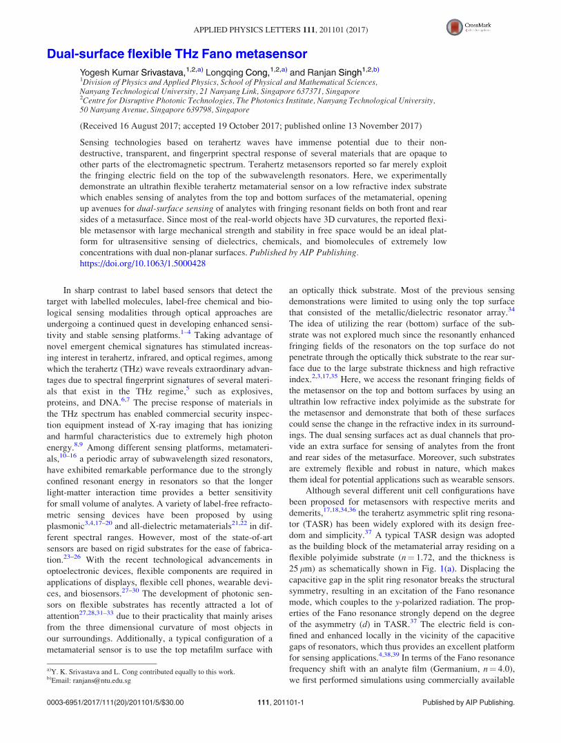
sensor surface, as illustrated in Figs. 1(a) and 1(c). The
corresponding results are plotted in Figs. 1(b) and 1(d), where
we observe a distinct spectral shift of Fano resonance in both
scenarios with only a 100 nm thick analyte, exhibiting the
dual-surface sensing.
In order to experimentally verify the dual-surface sensing
functionality of the metasensor, the sample was fabricated on a
25 lm thick polyimide substrate using conventional photoli-
thography, thermal evaporation of aluminum (200 nm thick),
and the lift-off process.40 The fabricated TASR array is shown
in Fig. 1(e). Owing to an excellent flexibility [see Fig. 1(f)],
thermal stability, and mechanical strength of the substrate,41,42
this type of metasensor would have valuable applications in
flexible optoelectronic sensing devices.
For refractometric sensing applications, a larger reso-
nance frequency shift is preferred while interacting with the
analyte, which thus requires a stronger local field concentra-
tion in the volume of the analyte layer according to the per-
turbation theory43
Dxi
xi¼ � 1
2
ðd~rDe ~rð ÞjE ~rð Þj2ð
d~re ~rð ÞjE ~rð Þj2; (1)
where Dxi is the frequency shift of eigenmode i at the reso-
nance frequency xi, Deð~rÞ is the change in analyte permittivity,
jEð~rÞj is the local field intensity, and eð~rÞ is the permittivity
of the analyte. Therefore, the refractometric sensitivity
(S ¼ ½Dxi=ðDna � xiÞ� � 100%, where Dna is the change in
the analyte refractive index) of a metasensor is proportional to
the field flux in the analyte, i.e., S /Ð
V jEð~rÞj2 � dV, where V
is volume of the electric field in the analyte.
In this context, we discuss the sensitivity performance
of Fano resonance with respect to the metasensor substrate
properties. According to the perturbation theory described by
Eq. (1), localized field intensity at Fano resonance deter-
mines the overall resonance frequency shift with a fixed
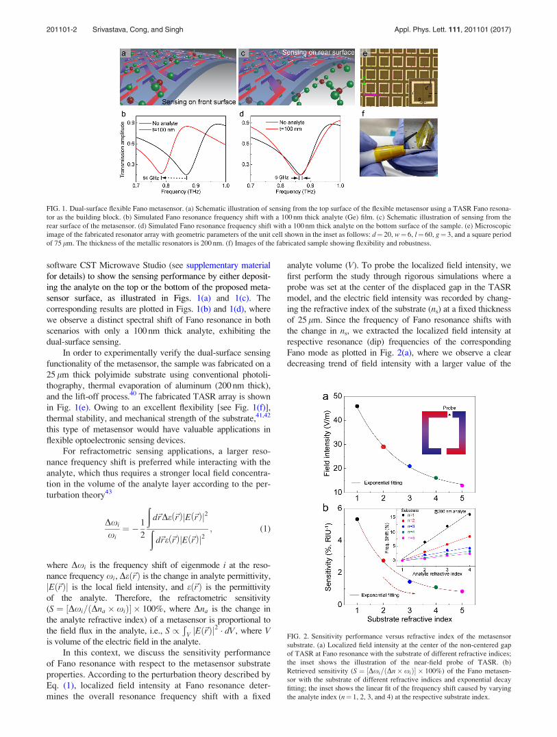
analyte volume (V). To probe the localized field intensity, we
first perform the study through rigorous simulations where a
probe was set at the center of the displaced gap in the TASR
model, and the electric field intensity was recorded by chang-
ing the refractive index of the substrate (ns) at a fixed thickness
of 25 lm. Since the frequency of Fano resonance shifts with
the change in ns, we extracted the localized field intensity at
respective resonance (dip) frequencies of the corresponding
Fano mode as plotted in Fig. 2(a), where we observe a clear
decreasing trend of field intensity with a larger value of the
FIG. 1. Dual-surface flexible Fano metasensor. (a) Schematic illustration of sensing from the top surface of the flexible metasensor using a TASR Fano resona-
tor as the building block. (b) Simulated Fano resonance frequency shift with a 100 nm thick analyte (Ge) film. (c) Schematic illustration of sensing from the
rear surface of the metasensor. (d) Simulated Fano resonance frequency shift with a 100 nm thick analyte on the bottom surface of the sample. (e) Microscopic
image of the fabricated resonator array with geometric parameters of the unit cell shown in the inset as follows: d¼ 20, w¼ 6, l¼ 60, g¼ 3, and a square period
of 75 lm. The thickness of the metallic resonators is 200 nm. (f) Images of the fabricated sample showing flexibility and robustness.
FIG. 2. Sensitivity performance versus refractive index of the metasensor
substrate. (a) Localized field intensity at the center of the non-centered gap
of TASR at Fano resonance with the substrate of different refractive indices;
the inset shows the illustration of the near-field probe of TASR. (b)
Retrieved sensitivity (S ¼ ½Dxi=ðDn�xiÞ� � 100%) of the Fano metasen-
sor with the substrate of different refractive indices and exponential decay
fitting; the inset shows the linear fit of the frequency shift caused by varying
the analyte index (n¼ 1, 2, 3, and 4) at the respective substrate index.
201101-2 Srivastava, Cong, and Singh Appl. Phys. Lett. 111, 201101 (2017)

substrate refractive index. An exponential decay of localized
electric field amplitude (jElj) was estimated at the capacitive
gap relative to ns, which is verified by an excellent numerical
fit with an equation jElj ¼ 65:1 � e�ns1:6 þ 10:5 V/m. This expo-
nential decay behavior of the localized electric field determines
the resonant frequency shift and sensitivity of the metasensor.
We then investigate the refractometric sensitivity (S) of the
proposed sensor by depositing a 200 nm thin-film analyte on
top of the metallic Fano resonator for different substrate refrac-
tive indices, and the sensitivity was retrieved by using a linear
fit as shown in the inset of Fig. 2(a). We note that the thickness
of the analyte film is around 1/2000 of the operating wave-
length at �0.8 THz (k¼ 375 lm) which is a deep subwave-
length regime. The respective sensitivities are plotted in Fig.
2(b), which also reveals a clear exponential decay trend
described by an equation S ¼ 10:8 � e�ns1:2 þ 0:67 RIU�1. The
exponential decay of the sensitivity is similar to the decay of
the electric field with an increasing substrate refractive index.
On the basis of the above observations, it is clear that a
lower refractive index substrate provides a better thin-film
sensitivity. Compared to the commonly used silicon substrate
(ns¼ 3.418),44 a flexible polyimide (ns¼ 1.72) is a better can-
didate for refractometric sensing so as to obtain a large sensi-
tivity. In order to clearly present the contrast of sensitivity
between these two configurations, we carried out simulations
and experiments using a TASR metamaterial array on two
different substrates. Fano resonance spectra were recorded in
a dry nitrogen atmosphere, by using a terahertz time-domain
spectroscopy (THz-TDS) system in the transmission mode. A
normalized transmission amplitude spectrum was obtained by
using j~tj ¼ j~tsam=~tref j, where ~tsam and ~tref are the Fourier
transformed frequency-domain transmission spectra of the
sample and reference (respective bare substrate of different
samples, i.e., polyimide and silicon), respectively. Here, we
chose to deposit a thin film of semiconductor material
Germanium (Ge) as the analyte due to its large refractive
index (n¼ 4.0), which provides a relatively large frequency
shift. The frequency shift of Fano resonance was clearly
observed by depositing different thicknesses of the Ge film
on top of the resonator array, and the simulated results are
plotted in Fig. 3(a) with 0 nm (without the analyte), 100 nm,
200 nm, and 300 nm Ge thin films on top of the metasensor
with polyimide and silicon substrates (inset graph). The Fano
frequency shift reveals a distinct contrast in the performance
of the metasensors on silicon and polyimide substrates. It is
observed that the metasensor on a lower index polyimide sub-
strate gives rise to a much improved and distinguishable fre-
quency shift compared to that on a silicon substrate as shown
in the inset of Fig. 3(a). The large resonance frequency shift
of the Fano resonator on a polyimide substrate originates
from its stronger localized field that enables a larger field flux
in an identical thickness of the analyte than that on a silicon
substrate. Such a large frequency shift of Fano resonance
induced by using a low index polyimide substrate was also
verified in experiments as shown in Fig. 3(b), which was
found to have a good agreement with the simulated results
except for a slight broadening of the resonance linewidth due
to larger loss in the experimental metamaterial system. By
using a lower index substrate, the sensitivity of a sensor is
clearly enhanced so that the resonance frequency shift of an
ultrathin film analyte can be easily resolved, which would
enhance the application potential of the metasensor in sensing
extremely low volumes of biomolecules. So far, we have dis-
cussed an enhanced sensitivity performance of the flexible
metasensor theoretically and experimentally on the basis of the
lower refractive index substrate. As a proof-of-concept, a low
index material, polyimide, was adopted for carrying out the
experiment. In addition to its advantage of the low refractive
index, polyimide also possesses excellent flexibility, robustness,
and thermal stability so that such a sensor could be applied in a
harsh environment for industrial systems. Its flexibility and
robustness also open up another possibility of further enhancing
its sensitivity by reducing the substrate thickness which is thin-
ner than the spatial extent of the resonant fringing fields.
According to the perturbation theory as discussed earlier
in Eq. (1), a strengthened localized electric field would give
rise to a large resonance frequency shift by changing the
refractive index of the surrounding medium. A commonly
adopted strategy for sensing is by directly placing the analyte
on top of resonators so as to exploit the enhanced local field
for a large field flux in the analyte since the fringing
field decays spatially above the metasurface. In this sensing
scheme, we can only utilize the top surface of the sensor, and
the other surface (bottom) becomes redundant due to an opti-
cally thick substrate with all the fringing field decaying within
the substrate material. In order to access the fringing fields on
the rear side of the substrate, the thickness of the substrate
must be reduced such that the fields could penetrate through
the analyte from the bottom surface (substrate side). However,
the commonly adopted rigid thicker substrates hinder the
access to the bottom surface fringing fields. A robust, thin,
and flexible polyimide substrate overcomes this limitation.
In Fig. 4(a), we show the simulated fringing electric
field intensity on both sides of a polyimide based Fano meta-
material sensor at the cut-plane as shown in the inset. The
metallic resonators are shown in yellow color, which was
FIG. 3. Experimental demonstration of thin-film sensing from the top sur-
face of the metasensor. (a) Simulated Fano resonance shift by changing the
thin-film analyte (Ge) thickness for the metasensor with a polyimide sub-
strate; the inset shows the Fano resonance shift by changing the analyte
thickness for the metasensor with a silicon substrate for comparison. (b)
Corresponding experimental Fano resonance shift of the metamaterial on a
polyimide substrate.
201101-3 Srivastava, Cong, and Singh Appl. Phys. Lett. 111, 201101 (2017)

considered as an ultrathin film (200 nm) at the zero point of
the z axis; the positive axis indicates the free space ambi-
ence, and the negative axis indicates the substrate space. As
shown in Fig. 4(a), the field intensity on both sides reveals
an exponential decay as a function of the spatial extent fol-
lowing jEnf j ¼ 49:0 � e z
2:2 þ 1:68 and jEpf j ¼ 37:1 � e� z
2:5 þ 0:93
on the negative (jEnf j) and positive axes (jEp
f j), respectively.
The localized field at the metamaterial surface reveals a
larger value on the substrate side compared to the free space
due to a relatively higher refractive index of the substrate,
and consequently, the spatial extent of the fringing field on
the substrate side is relatively short, which depends on the
refractive index of the substrate. An accessible spatial
distribution of the fringing electric field with a low index
polyimide substrate enable the detection of the analyte from
the bottom surface (substrate side) using the Fano reso-
nance of the metamaterial on a 25 lm thick polyimide sub-
strate. As shown in Fig. 4(b), we measured the frequency
shift of the Fano resonance with 100 nm Ge deposited on
the substrate side of the metasensor, which is also verified
by the simulated results shown in the inset. Thus, the dual-
surface sensing is enabled by the polyimide substrate based
metasensors.
A detailed study of the bottom surface sensing is per-
formed using rigorous simulations by varying the polyimide
substrate thickness. As per the exponential decay of the spa-
tial electric field, a thinner substrate provides a larger bottom
surface sensitivity for the analyte deposited on the bottom
surface of the substrate as indicated by the blue line in Fig.
4(c). The quality factor of Fano resonance also increases by
decreasing the substrate thickness due to reduced dissipation
in the lossy substrate. A Figure of Merit (FoM) parameter,
calculated by FoM ¼ S� Q, where S is the sensitivity and Qis the quality factor, indicates the overall sensing perfor-
mance. The calculated FoM values of Fano sensors with a
polyimide substrate at different thicknesses are also depicted
in Fig. 4(c), and it is clearly seen that the sensitivity is
enhanced in the case of thinner substrates. Our metasensor
design consists of a lower quality factor resonance due to the
limited energy confinement in the low-index substrate and
the large amplitude of the Fano resonance. Fano resonances
are weakly coupled to the free space and have extremely low
resonance amplitude, which pose the challenge in perform-
ing accurate measurements. Therefore, we enhanced the
asymmetry of the structure to excite a strong Fano resonance
which typically results in the broadening of its linewidth and
a decline in the Q factor.37
We further simulated the resultant Fano resonance shift
by depositing analyte on the top and bottom surfaces with a
100 nm thin-film of Germanium. As shown in Fig. 5(a), it is
visible that the total frequency shift of Fano resonance is
enhanced to 89 GHz. The total resonance shift is almost the
sum of the shift caused by individual surfaces (top: 84 GHz
and bottom: 6 GHz), which demonstrates the effect of an
additional sensing channel (surface).
The application of sensors on irregular surfaces of
three-dimensional objects is quite important. Thus, we also
FIG. 4. Spatial extent of fringing fields and bottom surface sensitivity of the
flexible metasensor. (a) Spatial distribution of the simulated fringing field on
both sides of the metamaterial on a polyimide substrate. (b) Experimental
and simulated Fano resonance shift by depositing 100 nm thin-film Ge on
the bottom surface of the sample. (c) Investigation of the bottom surface sen-
sitivity by changing the substrate thickness.
FIG. 5. Resonance shift by coating the analyte on both surfaces and the flex-
ibility test of the flexible metasensor. (a) Simulated Fano resonance shift
with a 100 nm analyte on both top and bottom surfaces of the flexible meta-
sensor. Dashed lines show the Fano spectra for the metasensor with the ana-
lyte only on top (blue) and bottom surfaces (pink) for comparison. (b)
Measured Fano spectra of the metasensor at different curvatures.
201101-4 Srivastava, Cong, and Singh Appl. Phys. Lett. 111, 201101 (2017)

performed the flexibility test on our metasensor at different
curvatures (j, j¼ 1/R, where R is the radius of the curved
sample, see supplementary material) and measured the spec-
tral responses as shown in Fig. 5(b). We observe a stable
Fano resonance frequency response with a slight modulation
in the transmission amplitude when the curvature is less than
0.85 cm�1. The stability of Fano resonance frequency starts
to deteriorate when curvature exceeds 0.85 cm�1 since the
resonator geometry, the array uniformity, and the density of
resonators get affected at larger curvature. The proposed
dual-surface metasensor would be a good candidate as a 3D
flexible sensor which could find practical applications.
In summary, we have experimentally demonstrated a
dual-surface terahertz metasensor on an ultrathin flexible
substrate with a low refractive index that reveals a highly
enhanced sensitivity. The ultrathin, low index, and flexible
design of the metasensor enables sensing of the analyte from
the top and bottom surfaces of the metamaterial. This flexi-
ble Fano sensor would open up a broader range of applica-
tions in industrial sensing systems and enable an enhanced
performance in biosensing with a lower molecule concentra-
tion. Such a sensor scheme could also to be extended into
different sensing configurations as per the on-demand
applications.
See supplementary material for the information on the
simulation methods and sample flexibility test.
The authors thank the Singapore Ministry of Education
Grant No. MOE2015-T2-2-103 for funding of this research.
1P. H. Siegel, IEEE Trans. Microwave Theory Tech. 52(10), 2438–2447
(2004).2J. N. Anker, W. P. Hall, O. Lyandres, N. C. Shah, J. Zhao, and R. P. Van
Duyne, Nat. Mater. 7(6), 442–453 (2008).3H. Im, H. Shao, Y. I. Park, V. M. Peterson, C. M. Castro, R. Weissleder,
and H. Lee, Nat. Biotechnol. 32(5), 490–495 (2014).4C. Wu, A. B. Khanikaev, R. Adato, N. Arju, A. A. Yanik, H. Altug, and G.
Shvets, Nat. Mater. 11(1), 69–75 (2012).5W. Withayachumnankul, G. M. Png, X. Yin, S. Atakaramians, I. Jones, H.
Lin, B. S. Y. Ung, J. Balakrishnan, B. W. H. Ng, B. Ferguson, S. P.
Mickan, B. M. Fischer, and D. Abbott, Proc. IEEE 95(8), 1528–1558
(2007).6J. Chen, Y. Chen, H. Zhao, G. J. Bastiaans, and X.-C. Zhang, Opt. Express
15(19), 12060–12067 (2007).7B. Fischer, M. Walther, and P. U. Jepsen, Phys. Med. Biol. 47(21), 3807
(2002).8Y. Shvyd’Ko, X-Ray Optics: High-Energy-Resolution Applications(Springer, 2013).
9X.-C. Zhang and J. Xu, Introduction to THz Wave Photonics (Springer,
2010).10D. R. Smith, J. B. Pendry, and M. C. Wiltshire, Science 305(5685),
788–792 (2004).11Y. Chen, I. A. I. Al-Naib, J. Gu, M. Wang, T. Ozaki, R. Morandotti, and
W. Zhang, AIP Adv. 2(2), 022109 (2012).12L. Xie, W. Gao, J. Shu, Y. Ying, and J. Kono, Sci. Rep. 5, 8671 (2015).13W. Xu, L. Xie, and Y. Ying, Nanoscale 9(37), 13864–13878 (2017).14M. Chen, L. Singh, N. Xu, R. Singh, W. Zhang, and L. Xie, Opt. Express
25(13), 14089–14097 (2017).
15M. Gupta, Y. K. Srivastava, M. Manjappa, and R. Singh, Appl. Phys. Lett.
110(12), 121108 (2017).16L. Cong, S. Tan, R. Yahiaoui, F. Yan, W. Zhang, and R. Singh, Appl.
Phys. Lett. 106(3), 031107 (2015).17N. Liu, M. Mesch, T. Weiss, M. Hentschel, and H. Giessen, Nano Lett.
10(7), 2342–2348 (2010).18N. Liu, T. Weiss, M. Mesch, L. Langguth, U. Eigenthaler, M. Hirscher, C.
S€onnichsen, and H. Giessen, Nano Lett. 10(4), 1103–1107 (2010).19A. Kabashin, P. Evans, S. Pastkovsky, W. Hendren, G. Wurtz, R.
Atkinson, R. Pollard, V. Podolskiy, and A. Zayats, Nat. Mater. 8(11),
867–871 (2009).20N. Born, I. Al-Naib, C. Jansen, R. Singh, J. V. Moloney, M. Scheller, and
M. Koch, Adv. Opt. Mater. 3(5), 642–645 (2015).21Y. Yang, I. I. Kravchenko, D. P. Briggs, and J. Valentine, Nat. Commun.
5, 5753 (2014).22A. I. Kuznetsov, A. E. Miroshnichenko, M. L. Brongersma, Y. S. Kivshar,
and B. Luk’yanchuk, Science 354(6314), aag2472 (2016).23A. Ebrahimi, W. Withayachumnankul, S. Al-Sarawi, and D. Abbott, IEEE
Sens. J. 14(5), 1345–1351 (2014).24I. A. I. Al-Naib, C. Jansen, and M. Koch, Appl. Phys. Lett. 93(8), 083507
(2008).25I. Al-Naib, IEEE J. Sel. Top. Quantum Electron. 23(4), 1–5 (2017).26B. Reinhard, K. M. Schmitt, V. Wollrab, J. Neu, R. Beigang, and M.
Rahm, Appl. Phys. Lett. 100(22), 221101 (2012).27J. A. Rogers, T. Someya, and Y. Huang, Science 327(5973), 1603–1607
(2010).28D.-H. Kim, N. Lu, R. Ma, Y.-S. Kim, R.-H. Kim, S. Wang, J. Wu, S. M.
Won, H. Tao, A. Islam, K. J. Yu, T.-i. Kim, R. Chowdhury, M. Ying, L.
Xu, M. Li, H.-J. Chung, H. Keum, M. McCormick, P. Liu, Y.-W. Zhang,
F. G. Omenetto, Y. Huang, T. Coleman, and J. A. Rogers, Science
333(6044), 838–843 (2011).29T. Aernouts, P. Vanlaeke, W. Geens, J. Poortmans, P. Heremans, S.
Borghs, R. Mertens, R. Andriessen, and L. Leenders, Thin Solid Films
451–452, 22–25 (2004).30H. Tao, L. R. Chieffo, M. A. Brenckle, S. M. Siebert, M. Liu, A. C.
Strikwerda, K. Fan, D. L. Kaplan, X. Zhang, R. D. Averitt, and F. G.
Omenetto, Adv. Mater. 23(28), 3197–3201 (2011).31L. Cong, Y. K. Srivastava, A. Solanki, T. C. Sum, and R. Singh, ACS
Photonics 4(7), 1595–1601 (2017).32A. Sadeqi, H. R. Nejad, and S. Sonkusale, Opt. Express 25(14),
16092–16100 (2017).33R. Yahiaoui, S. Tan, L. Cong, R. Singh, F. Yan, and W. Zhang, J. Appl.
Phys. 118(8), 083103 (2015).34H. Tao, A. C. Strikwerda, M. Liu, J. P. Mondia, E. Ekmekci, K. Fan, D. L.
Kaplan, W. J. Padilla, X. Zhang, R. D. Averitt, and F. G. Omenetto, Appl.
Phys. Lett. 97(26), 261909 (2010).35K. V. Sreekanth, Y. Alapan, M. ElKabbash, E. Ilker, M. Hinczewski,
U. A. Gurkan, A. De Luca, and G. Strangi, Nat. Mater. 15(6), 621–627
(2016).36E. Cubukcu, S. Zhang, Y.-S. Park, G. Bartal, and X. Zhang, Appl. Phys.
Lett. 95(4), 043113 (2009).37L. Cong, M. Manjappa, N. Xu, I. Al-Naib, W. Zhang, and R. Singh, Adv.
Opt. Mater. 3(11), 1537–1543 (2015).38B. Luk’yanchuk, N. I. Zheludev, S. A. Maier, N. J. Halas, P. Nordlander,
H. Giessen, and C. T. Chong, Nat. Mater. 9(9), 707–715 (2010).39R. Singh, W. Cao, I. Al-Naib, L. Cong, W. Withayachumnankul, and W.
Zhang, Appl. Phys. Lett. 105(17), 171101 (2014).40S. Walia, C. M. Shah, P. Gutruf, H. Nili, D. R. Chowdhury, W.
Withayachumnankul, M. Bhaskaran, and S. Sriram, Appl. Phys. Rev. 2(1),
011303 (2015).41W. A. MacDonald, M. K. Looney, D. MacKerron, R. Eveson, R. Adam,
K. Hashimoto, and K. Rakos, J. Soc. Inf. Disp. 15(12), 1075–1083 (2007).42W. A. MacDonald, J. Mater. Chem. 14(1), 4–10 (2004).43W. Zhang and O. J. F. Martin, ACS Photonics 2(1), 144–150 (2015).44J. Dai, J. Zhang, W. Zhang, and D. Grischkowsky, J. Opt. Soc. Am. B
21(7), 1379–1386 (2004).
201101-5 Srivastava, Cong, and Singh Appl. Phys. Lett. 111, 201101 (2017)