dual power distribution switches enable …
TRANSCRIPT

1FEATURES
DESCRIPTION
TPS2080, TPS2081, TPS2082 DUALTPS2085, TPS2086, TPS2087 QUADSLVS202B–SEPTEMBER 2000–REVISED OCTOBER 2007
www.ti.com
POWER-DISTRIBUTION SWITCHES
• 80-mΩ High-Side MOSFET Switch• 500 mA Continuous Current per Channel• Independent Thermal and Short-Circuit
Protection With Overcurrent Logic Output• Operating Range: 2.7-V to 5.5-V• CMOS- and TTL-Compatible Enable Inputs• 2.5-ms Typical Rise Time• Undervoltage Lockout• 10 μA Maximum Standby Supply Current• Bidirectional Switch• Available in 8-Pin and 16-Pin SOIC Packages• Ambient Temperature Range, 0°C to 85°C• ESD Protection
The TPS2080, TPS2081, and TPS2082 dual and theTPS2085, TPS2086 and TPS2087 quadpower-distribution switches are intended forapplications where heavy capacitive loads and shortcircuits are likely to be encountered.
The TPS208x devices incorporate 80-mΩ N-channel MOSFET high-side power switches for power-distributionsystems that require multiple power switches in a single package. Each switch is controlled by an independentlogic enable input. Gate drive is provided by an internal charge pump designed to control the power-switch risetimes and fall times to minimize current surges during switching. The charge pump requires no externalcomponents and allows operation from supplies as low as 2.7 V.
When the output load exceeds the current-limit threshold or a short is present, the TPS208x limits the outputcurrent to a safe level by switching into a constant-current mode, pulling the overcurrent (OCx) logic output low.When continuous heavy overloads and short circuits increase the power dissipation in the switch causing thejunction temperature to rise, a thermal protection circuit shuts off the switch to prevent damage. Recovery from athermal shutdown is automatic once the device has cooled sufficiently. Internal circuitry ensures the switchremains off until valid input voltage is present. The TPS208x devices are designed to current limit at 1.0-A load.
1
Please be aware that an important notice concerning availability, standard warranty, and use in critical applications ofTexas Instruments semiconductor products and disclaimers thereto appears at the end of this data sheet.
PRODUCTION DATA information is current as of publication date. Copyright © 2000–2007, Texas Instruments IncorporatedProducts conform to specifications per the terms of the TexasInstruments standard warranty. Production processing does notnecessarily include testing of all parameters.

www.ti.com
TPS2080, TPS2081, TPS2082 DUALTPS2085, TPS2086, TPS2087 QUADSLVS202B–SEPTEMBER 2000–REVISED OCTOBER 2007
These devices have limited built-in ESD protection. The leads should be shorted together or the device placed in conductive foamduring storage or handling to prevent electrostatic damage to the MOS gates.
AVAILABLE OPTIONS (1)
DUAL POWER DISTRIBUTION SWITCHESTYPICAL PACKAGEDRECOMMENDEDENABLE SHORT-CIRCUIT DEVICESMAXIMUM
CURRENT LIMITTA CONTINUOUS LOAD SMALLAT 25°CCURRENTEN1 EN2 OUTLINE(A)(A) (D) (2)
Active high Active high TPS2080D0°C to 85°C Active high Active low 0.5 1.0 TPS2081D
Active low Active low TPS2082DQUAD POWER DISTRIBUTION SWITCHES
ENABLE RECOMMENDED TYPICAL PACKAGEDMAXIMUM SHORT-CIRCUIT DEVICES
CONTINUOUS LOAD CURRENT LIMITTA SMALLCURRENT AT 25°CEN1 EN2 EN3 DN4 OUTLINE(A) (A) (D) (2)
Active high Active high Active high Active high TPS2085D0°C to 85°C Active high Active low Active high Active low 0.5 1.0 TPS2086D
Active low Active low Active low Active low TPS2087D
(1) For the most current package and ordering information, see the Package Option Addendum at the end of this document, or see the TIwebsite at www.ti.com.
(2) The D package is available taped and reeled. Add an R suffix to device type (e.g., TPS2081DR).
2 Submit Documentation Feedback Copyright © 2000–2007, Texas Instruments Incorporated
Product Folder Link(s): TPS2080, TPS2081, TPS2082 DUAL TPS2085, TPS2086, TPS2087 QUAD

www.ti.com
TPS2080, TPS2081, TPS2082 DUALTPS2085, TPS2086, TPS2087 QUADSLVS202B–SEPTEMBER 2000–REVISED OCTOBER 2007
TPS2082 FUNCTIONAL BLOCK DIAGRAM
Copyright © 2000–2007, Texas Instruments Incorporated Submit Documentation Feedback 3
Product Folder Link(s): TPS2080, TPS2081, TPS2082 DUAL TPS2085, TPS2086, TPS2087 QUAD

www.ti.com
TPS2080, TPS2081, TPS2082 DUALTPS2085, TPS2086, TPS2087 QUADSLVS202B–SEPTEMBER 2000–REVISED OCTOBER 2007
TPS2087 FUNCTIONAL BLOCK DIAGRAM
4 Submit Documentation Feedback Copyright © 2000–2007, Texas Instruments Incorporated
Product Folder Link(s): TPS2080, TPS2081, TPS2082 DUAL TPS2085, TPS2086, TPS2087 QUAD

www.ti.com
TPS2080, TPS2081, TPS2082 DUALTPS2085, TPS2086, TPS2087 QUADSLVS202B–SEPTEMBER 2000–REVISED OCTOBER 2007
TERMINAL FUNCTIONSDUAL POWER-DISTRIBUTION SWITCHES
TERMINALNO. I/O DESCRIPTION
NAMETPS2080 TPS2081 TPS2082
EN1 4 I Enable input. Active low turns on power switch.EN2 5 5 I Enable input. Active low turns on power switch.EN1 4 4 I Enable input. Active high turns on power switch.EN2 5 I Enable input. Active high turns on power switch.GND 1 1 1 I GroundIN1 2 2 2 I N-Channel MOSFET DrainIN2 3 3 3 I N-Channel MOSFET DrainOC 8 8 8 O Overcurrent. Open drain output active lowOUT1 7 7 7 O Power-switch outputOUT2 6 6 6 O Power-switch output
QUAD POWER-DISTRIBUTION SWITCHESTERMINAL
NO. I/O DESCRIPTIONNAME
TPS2085 TPS2086 TPS2087EN1 4 I Enable input. Active low turns on power switch.EN2 13 13 I Enable input. Active low turns on power switch.EN3 8 I Enable input. Active low turns on power switch.EN4 9 9 I Enable input. Active low turns on power switch.EN1 4 4 I Enable input. Active high turns on power switch.EN2 13 I Enable input. Active high turns on power switch.EN3 8 8 I Enable input. Active high turns on power switch.EN4 9 I Enable input. Active high turns on power switch.GNDA 1 1 1 Ground for IN1 and IN2 switch and circuitryGNDB 5 5 5 Ground for IN3 and IN4 switch and circuitryIN1 2 2 2 I N-channel MOSFET drainIN2 3 3 3 I N-channel MOSFET drainIN3 6 6 6 I N-channel MOSFET drainIN4 7 7 7 I N-channel MOSFET drainOCA 16 16 16 O Overcurrent indicator for switch 1 and switch 2. Active-low open drain output.OCB 12 12 12 O Overcurrent indicator for switch 3 and switch 4. Active low open drain outputOUT1 15 15 15 O Power-switch outputOUT2 14 14 14 O Power-switch outputOUT3 11 11 11 O Power-switch outputOUT4 10 10 10 O Power-switch output
Copyright © 2000–2007, Texas Instruments Incorporated Submit Documentation Feedback 5
Product Folder Link(s): TPS2080, TPS2081, TPS2082 DUAL TPS2085, TPS2086, TPS2087 QUAD

www.ti.com
DETAILED DESCRIPTION
POWER SWITCH
CHARGE PUMP
DRIVER
ENABLE (ENx or ENx)
OVERCURRENT (OCx)
CURRENT SENSE
THERMAL SENSE
UNDERVOLTAGE LOCKOUT
TPS2080, TPS2081, TPS2082 DUALTPS2085, TPS2086, TPS2087 QUADSLVS202B–SEPTEMBER 2000–REVISED OCTOBER 2007
The power switch is an N-channel MOSFET with a maximum on-state resistance of 135 mΩ (VI(IN) = 5V).Configured as a high-side switch, the power switch prevents current flow from OUTx to IN and IN to OUTx whendisabled. The power switch supplies a minimum of 500 mA per switch.
An internal charge pump supplies power to the driver circuit and provides the necessary voltage to pull the gateof the MOSFET above the source. The charge pump operates from input voltages as low as 2.7V and requiresvery little supply current.
The driver controls the gate voltage of the power switch. To limit large current surges and reduce the associatedelectromagnetic interference (EMI) produced, the driver incorporates circuitry that controls the rise times and falltimes of the output voltage. The rise and fall times are typically in the 2-ms to 4-ms range.
The logic enable disables the power switch and the bias for the charge pump, driver, and other circuitry to reducethe supply current to less than 10 μA when a logic high is present on ENx or a logic low is present on ENx. Alogic low input on ENx or logic high on ENx restores bias to the drive and control circuits and turns the power on.The enable input is compatible with both TTL and CMOS logic levels.
The OCx open drain output is asserted (active low) when an overcurrent or over temperature condition isencountered. The output will remain asserted until the overcurrent or overtemperature condition is removed.
A sense FET monitors the current supplied to the load. The sense FET measures current more efficiently thanconventional resistance methods. When an overload or short circuit is encountered, the current-sense circuitrysends a control signal to the driver. The driver in turn reduces the gate voltage and drives the power FET into itssaturation region, which switches the output into a constant current mode and holds the current constant whilevarying the voltage on the load.
The TPS208x implements a dual thermal trip to allow fully independent operation of the power distributionswitches. In an overcurrent or short-circuit condition the junction temperature rises. When the die temperaturerises to approximately 140°C, the internal thermal sense circuitry checks to determine which power switch is inan overcurrent condition and turns off that switch, thus isolating the fault without interrupting operation of theadjacent power switch. Hysteresis is built into the thermal sense, and after the device has cooled approximately20 degrees, the switch turns back on. The switch continues to cycle off and on until the fault is removed. The(OCx) open-drain output is asserted (active low) when overtemperature or overcurrent occurs.
A voltage sense circuit monitors the input voltage. When the input voltage is below approximately 2 V, a controlsignal turns off the power switch.
6 Submit Documentation Feedback Copyright © 2000–2007, Texas Instruments Incorporated
Product Folder Link(s): TPS2080, TPS2081, TPS2082 DUAL TPS2085, TPS2086, TPS2087 QUAD

www.ti.com
ABSOLUTE MAXIMUM RATINGS
DISSIPATION RATINGS TABLE
RECOMMENDED OPERATING CONDITIONS
ELECTRICAL CHARACTERISTICS
TPS2080, TPS2081, TPS2082 DUALTPS2085, TPS2086, TPS2087 QUADSLVS202B–SEPTEMBER 2000–REVISED OCTOBER 2007
over operating free-air temperature range (unless otherwise noted) (1)
VALUE UNITVI(IN) Input voltage range (2) –0.3 to 6 VVO(OUTx) Output voltage range (2) –0.3 to VI(IN) + 0.3 VVI(ENx) or VI(ENx) Input voltage range –0.3 to 6 VIO(OUTx) Continuous output current Internally Limited
Continuous total power dissipation See Dissipation Rating TableTJ Operating virtual junction temperature range 0 to 125 °CTstg Storage temperature range –65 to 150 °C
Lead temperature soldering 1,6 mm (1/16 inch) from case for 10 seconds 260 °CHuman body model 2 kV
ESD Electrostatic discharge protection Machine model 200 VCharged device model (CDM) 750 V
(1) Stresses beyond those listed under absolute maximum ratings may cause permanent damage to the device. These are stress ratingsonly, and functional operation of the device at these or any other conditions beyond those indicated under recommended operatingconditions is not implied. Exposure to absolute-maximum-rated conditions for extended periods may affect device reliability.
(2) All voltages are with respect to GND.
TA ≤ 25°C DERATING FACTOR TA = 70°C TA = 85°CPACKAGE POWER RATING ABOVE TA = 25°C POWER RATING POWER RATING=D-8 725 mW 5.8 mW/°C 464 mW 377 mWD-16 1123 mW 9 mW/°C 719 mW 584 mW
MIN MAX UNITVI(IN) Input voltage 2.7 5.5 VVI(ENx) or VI(ENx) Input voltage 0 5.5 VIO Continuous output current (per switch) 0 500 mATJ Operating virtual junction temperature 0 125 °C
over recommended operating junction temperature range, VI(IN) = 5.5 V, IO = rated current, VI(ENx) = 0 V, VI(ENx) = VI(INx) (unlessotherwise noted)
SUPPLY CURRENTPARAMETER TEST CONDITIONS MIN TYP MAX UNIT
VI(ENx) = VI(IN), TJ = 25°C 0.025 1Supply current, low-level No Load on OUT μAVI(ENx) = 0 Voutput –40°C ≤ TJ ≤ 125°C 10Supply current, high-level VI(ENx) = 0 V, TJ = 25°C 85 110
No Load on OUT μAoutput VI(ENx) = VI(IN) –40°C ≤ TJ ≤ 125°C 100VI(ENx) = VI(IN),Leakage current OUT connected to ground –40°C ≤ TJ ≤ 125°C 100 μAVI(ENx) = 0 VVI(ENx) = 0 V,Reverse leakage current INx = high impedance TJ = 25°C 0.3 μAVI(ENx) = VI(IN)
Copyright © 2000–2007, Texas Instruments Incorporated Submit Documentation Feedback 7
Product Folder Link(s): TPS2080, TPS2081, TPS2082 DUAL TPS2085, TPS2086, TPS2087 QUAD

www.ti.com
ELECTRICAL CHARACTERISTICS (Continued)
TPS2080, TPS2081, TPS2082 DUALTPS2085, TPS2086, TPS2087 QUADSLVS202B–SEPTEMBER 2000–REVISED OCTOBER 2007
over recommended operating junction temperature range, VI(IN) = 5.5 V, IO = rated current, VI(ENx) = 0 V, VI(ENx) = VI(INx) (unlessotherwise noted)
POWER SWITCHPARAMETER TEST CONDITIONS (1) MIN TYP MAX UNIT
VI(IN) = 5 V, TJ = 25°C, IO = 0.5 A 80 100VI(IN) = 5 V, TJ = 85°C, IO = 0.5 A 90 120VI(IN) = 5 V, TJ = 125°C, IO = 0.5 A 100 135Static drain-source on-staterDS(on) mΩresistance VI(IN) = 3.3 V, TJ = 25°C, IO = 0.5 A 90 125VI(IN) = 3.3 V, TJ = 85°C, IO = 0.5 A 110 145VI(IN) = 3.3 V, TJ = 125°C, IO = 0.5 A 120 165VI(IN) = 5.5 V, RL = 10Ω, TJ = 125°C, CL = 1 μF 2.5
tr Rise time, output msVI(IN) = 2.7 V, RL = 10Ω, TJ = 125°C, CL = 1 μF 3VI(IN) = 5.5 V, RL = 10Ω, TJ = 125°C, CL = 1 μF 4.4
tf Fall time, output msVI(IN) = 2.7 V, RL = 10Ω, TJ = 125°C, CL = 1 μF 2.5
(1) Pulse-testing techniques maintain junction temperature close to ambient temperature; thermal effects must be taken into accountseparately.
ENABLE INPUT VI(ENx) or VI(ENx)
PARAMETER TEST CONDITIONS MIN TYP MAX UNITVIH High-level input voltage 2.7 V ≤ VI(IN) ≤ 5.5 V 2 V
4.5 V ≤ VI(IN) ≤ 5.5 V 0.8VIL Low-level input voltage V
2.7 V ≤ VI(IN) ≤ 4.5 V 0.4II Input current VI(ENx) = 0 V and VI(ENx) = VI(IN), or VI(ENx) = VI(IN) and VI(ENx) = 0 V –0.5 0.5 μAton Turnon time CL = 100 μF, RL = 10 μF 20 mstoff Turnon time CL = 100 μF, RL = 10 μF 40 ms
CURRENT LIMITPARAMETER TEST CONDITIONS (1) MIN TYP MAX UNIT
VI(IN) = 5 V, OUT connected to GND,IOS Short-circuit output current 0.7 1 1.3 ADevice enabled into short circuit
(1) Pulse-testing techniques maintain junction temperature close to ambient temperature; thermal effects must be taken into accountseparately.
UNDERVOLTAGE LOCKOUTPARAMETER TEST CONDITIONS MIN TYP MAX UNIT
Low-level input voltage 2 2.5 VHysteresis TJ = 25°C 100 mV
OVERCURRENT OCxPARAMETER TEST CONDITIONS MIN TYP MAX UNIT
Sink current (1) VO = 5 V 10 mAOutput low voltage IO = 5 mA, VOL(OCx) 0.5 VOff-state current (1) VO = 5 V, VO = 3.3 V 1 μA
(1) Specified by design, not production tested.
8 Submit Documentation Feedback Copyright © 2000–2007, Texas Instruments Incorporated
Product Folder Link(s): TPS2080, TPS2081, TPS2082 DUAL TPS2085, TPS2086, TPS2087 QUAD

www.ti.com
PARAMETER MEASUREMENT INFORMATION
TPS2080, TPS2081, TPS2082 DUALTPS2085, TPS2086, TPS2087 QUADSLVS202B–SEPTEMBER 2000–REVISED OCTOBER 2007
Figure 1. Test Circuit and Voltage Waveforms
Figure 2. Turnon Delay and Rise Time With 0.1-μF Load Figure 3. Turnoff Delay and Fall Time With 0.1-μF Load
Copyright © 2000–2007, Texas Instruments Incorporated Submit Documentation Feedback 9
Product Folder Link(s): TPS2080, TPS2081, TPS2082 DUAL TPS2085, TPS2086, TPS2087 QUAD

www.ti.com
TPS2080, TPS2081, TPS2082 DUALTPS2085, TPS2086, TPS2087 QUADSLVS202B–SEPTEMBER 2000–REVISED OCTOBER 2007
PARAMETER MEASUREMENT INFORMATION (continued)
Figure 4. Turnon Delay and Rise Time With 1-μF Load Figure 5. Turnoff Delay and Fall Time With 1-μF Load
Figure 6. TPS2080, Short-Circuit Current, Device Figure 7. TPS2080, Threshold Trip Current With RampedEnabled Into Short Load on Enabled Device
10 Submit Documentation Feedback Copyright © 2000–2007, Texas Instruments Incorporated
Product Folder Link(s): TPS2080, TPS2081, TPS2082 DUAL TPS2085, TPS2086, TPS2087 QUAD

www.ti.com
TPS2080, TPS2081, TPS2082 DUALTPS2085, TPS2086, TPS2087 QUADSLVS202B–SEPTEMBER 2000–REVISED OCTOBER 2007
PARAMETER MEASUREMENT INFORMATION (continued)
Figure 8. OC Response With Ramped Load on Enabled Figure 9. Inrush Current With 100-μF, 220-μF and 470-μFDevice Load Capacitance
Figure 10. 4-Ω Load Connected to Enabled Device Figure 11. 1-Ω Load Connected to Enabled Device
Copyright © 2000–2007, Texas Instruments Incorporated Submit Documentation Feedback 11
Product Folder Link(s): TPS2080, TPS2081, TPS2082 DUAL TPS2085, TPS2086, TPS2087 QUAD

www.ti.com
TYPICAL CHARACTERISTICS
TPS2080, TPS2081, TPS2082 DUALTPS2085, TPS2086, TPS2087 QUADSLVS202B–SEPTEMBER 2000–REVISED OCTOBER 2007
TURNON DELAY TIME TURNOFF DELAY TIMEvs vs
INPUT VOLTAGE INPUT VOLTAGE
Figure 12. Figure 13.
RISE TIME FALL TIMEvs vs
INPUT VOLTAGE INPUT VOLTAGE
Figure 14. Figure 15.
12 Submit Documentation Feedback Copyright © 2000–2007, Texas Instruments Incorporated
Product Folder Link(s): TPS2080, TPS2081, TPS2082 DUAL TPS2085, TPS2086, TPS2087 QUAD

www.ti.com
TPS2080, TPS2081, TPS2082 DUALTPS2085, TPS2086, TPS2087 QUADSLVS202B–SEPTEMBER 2000–REVISED OCTOBER 2007
TYPICAL CHARACTERISTICS (continued)
SUPPLY CURRENT, OUTPUT ENABLED SUPPLY CURRENT, OUTPUT DISABLEDvs vs
JUNCTION TEMPERATURE JUNCTION TEMPERATURE
Figure 16. Figure 17.
STATIC DRAIN-SOURCE ON-STATE RESISTANCE INPUT-TO-OUTPUT VOLTAGEvs vs
JUNCTION TEMPERATURE LOAD CURRENT
Figure 18. Figure 19.
Copyright © 2000–2007, Texas Instruments Incorporated Submit Documentation Feedback 13
Product Folder Link(s): TPS2080, TPS2081, TPS2082 DUAL TPS2085, TPS2086, TPS2087 QUAD

www.ti.com
TPS2080, TPS2081, TPS2082 DUALTPS2085, TPS2086, TPS2087 QUADSLVS202B–SEPTEMBER 2000–REVISED OCTOBER 2007
TYPICAL CHARACTERISTICS (continued)
SHORT-CIRCUIT OUTPUT CURRENT THRESHOLD TRIP CURRENTvs vs
JUNCTION TEMPERATURE INPUT VOLTAGE
Figure 20. Figure 21.
UNDERVOLTAGE LOCKOUT CURRENT LIMIT RESPONSEvs vs
JUNCTION TEMPERATURE PEAK CURRENT
Figure 22. Figure 23.
14 Submit Documentation Feedback Copyright © 2000–2007, Texas Instruments Incorporated
Product Folder Link(s): TPS2080, TPS2081, TPS2082 DUAL TPS2085, TPS2086, TPS2087 QUAD

www.ti.com
APPLICATION INFORMATION
POWER-SUPPLY CONSIDERATIONS
OVERCURRENT
OC RESPONSES
TPS2080, TPS2081, TPS2082 DUALTPS2085, TPS2086, TPS2087 QUADSLVS202B–SEPTEMBER 2000–REVISED OCTOBER 2007
Figure 24. Typical Application
A 0.01-μF to 0.1-μF ceramic bypass capacitor between INx and GND, close to the device, is recommended.Placing a high-value electrolytic capacitor on the output pin(s) is recommended when the output load is heavy.This precaution reduces power-supply transients that may cause ringing on the input. Additionally, bypassing theoutput with a 0.01-μF to 0.1-μF ceramic capacitor improves the immunity of the device to short-circuit transients.
A sense FET is employed to check for overcurrent conditions. Unlike current-sense resistors, sense FETs do notincrease the series resistance of the current path. When an overcurrent condition is detected, the devicemaintains a constant output current and reduces the output voltage accordingly. Complete shutdown occurs onlyif the fault is present long enough to activate thermal limiting.
Three possible overload conditions can occur. In the first condition, the output has been shorted before thedevice is enabled or before VI(IN) has been applied (see Figure 6). The TPS208x senses the short andimmediately switches into a constant-current output.
In the second condition, a short or an overload occurs while the device is enabled. At the instant the overloadoccurs, very high currents may flow for a short time before the current-limit circuit can react (see Figure 10 andFigure 11). After the current-limit circuit has tripped (reached the overcurrent trip threshold) the device switchesinto constant-current mode.
In the third condition, the load has been gradually increased beyond the recommended operating current. Thecurrent is permitted to rise until the current-limit threshold is reached or until the thermal limit of the device isexceeded (see Figure 8). The TPS208x is capable of delivering current up to the current-limit threshold withoutdamaging the device. Once the threshold has been reached, the device switches into its constant-current mode.
The OC open-drain output is asserted (active low) when an overcurrent or overtemperature condition isencountered. The output will remain asserted until the overcurrent or overtemperature condition is removed.Connecting a heavy capacitive load to an enabled device can cause momentary false overcurrent reporting fromthe inrush current flowing through the device, charging the downstream capacitor. The TPS208x devices aredesigned to reduce false overcurrent reporting. An internal overcurrent transient filter eliminates the need to useexternal components to remove unwanted pulses. Using low-ESR electrolytic capacitors on the output lowers theinrush current flow through the device during hot-plug events by providing a low impedance energy source,thereby reducing erroneous overcurrent reporting.
Copyright © 2000–2007, Texas Instruments Incorporated Submit Documentation Feedback 15
Product Folder Link(s): TPS2080, TPS2081, TPS2082 DUAL TPS2085, TPS2086, TPS2087 QUAD
www.ti.com
POWER DISSIPATION AND JUNCTION TEMPERATURE
THERMAL PROTECTION
TPS2080, TPS2081, TPS2082 DUALTPS2085, TPS2086, TPS2087 QUADSLVS202B–SEPTEMBER 2000–REVISED OCTOBER 2007
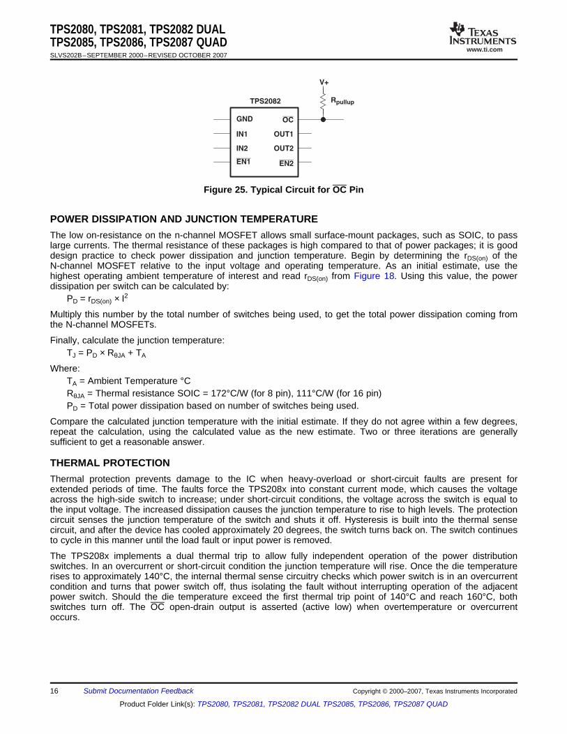
Figure 25. Typical Circuit for OC Pin
The low on-resistance on the n-channel MOSFET allows small surface-mount packages, such as SOIC, to passlarge currents. The thermal resistance of these packages is high compared to that of power packages; it is gooddesign practice to check power dissipation and junction temperature. Begin by determining the rDS(on) of theN-channel MOSFET relative to the input voltage and operating temperature. As an initial estimate, use thehighest operating ambient temperature of interest and read rDS(on) from Figure 18. Using this value, the powerdissipation per switch can be calculated by:
PD = rDS(on) × I2
Multiply this number by the total number of switches being used, to get the total power dissipation coming fromthe N-channel MOSFETs.
Finally, calculate the junction temperature:TJ = PD × RθJA + TA
Where:TA = Ambient Temperature °CRθJA = Thermal resistance SOIC = 172°C/W (for 8 pin), 111°C/W (for 16 pin)PD = Total power dissipation based on number of switches being used.
Compare the calculated junction temperature with the initial estimate. If they do not agree within a few degrees,repeat the calculation, using the calculated value as the new estimate. Two or three iterations are generallysufficient to get a reasonable answer.
Thermal protection prevents damage to the IC when heavy-overload or short-circuit faults are present forextended periods of time. The faults force the TPS208x into constant current mode, which causes the voltageacross the high-side switch to increase; under short-circuit conditions, the voltage across the switch is equal tothe input voltage. The increased dissipation causes the junction temperature to rise to high levels. The protectioncircuit senses the junction temperature of the switch and shuts it off. Hysteresis is built into the thermal sensecircuit, and after the device has cooled approximately 20 degrees, the switch turns back on. The switch continuesto cycle in this manner until the load fault or input power is removed.
The TPS208x implements a dual thermal trip to allow fully independent operation of the power distributionswitches. In an overcurrent or short-circuit condition the junction temperature will rise. Once the die temperaturerises to approximately 140°C, the internal thermal sense circuitry checks which power switch is in an overcurrentcondition and turns that power switch off, thus isolating the fault without interrupting operation of the adjacentpower switch. Should the die temperature exceed the first thermal trip point of 140°C and reach 160°C, bothswitches turn off. The OC open-drain output is asserted (active low) when overtemperature or overcurrentoccurs.
16 Submit Documentation Feedback Copyright © 2000–2007, Texas Instruments Incorporated
Product Folder Link(s): TPS2080, TPS2081, TPS2082 DUAL TPS2085, TPS2086, TPS2087 QUAD

www.ti.com
UNDERVOLTAGE LOCKOUT (UVLO)l
GENERIC HOT-PLUG APPLICATIONS (see Figure 26)
TPS2080, TPS2081, TPS2082 DUALTPS2085, TPS2086, TPS2087 QUADSLVS202B–SEPTEMBER 2000–REVISED OCTOBER 2007
An undervoltage lockout ensures that the power switch is in the off state at power up. Whenever the inputvoltage falls below approximately 2 V, the power switch will be quickly turned off. This facilitates the design ofhot-insertion systems where it is not possible to turn off the power switch before input power is removed. TheUVLO will also keep the switch from being turned on until the power supply has reached at least 2 V, even if theswitch is enabled. Upon reinsertion, the power switch will be turned on with a controlled rise time to reduce EMIand voltage overshoots.
In many applications it may be necessary to remove modules or pc boards while the main unit is still operating.These are considered hot-plug applications. Such implementations require the control of current surges seen bythe main power supply and the card being inserted. The most effective way to control these surges is to limit andslowly ramp the current and voltage being applied to the card, similar to the way in which a power supplynormally turns on. Due to the controlled rise times and fall times of the TPS208x, these devices can be used toprovide a softer start-up to devices being hot-plugged into a powered system. The UVLO feature of the TPS208xalso ensures the switch will be off after the card has been removed, and the switch will be off during the nextinsertion. The UVLO feature insures a soft start with a controlled rise time for every insertion of the card ormodule.
Figure 26. Typical Hot-Plug Implementation
By placing the TPS208x between the VCC input and the rest of the circuitry, the input power will reach thesedevices first after insertion. The typical rise time of the switch is approximately 2.5 ms, providing a slow voltageramp at the output of the device. This implementation controls system surge currents and provides ahot-plugging mechanism for any device.
Copyright © 2000–2007, Texas Instruments Incorporated Submit Documentation Feedback 17
Product Folder Link(s): TPS2080, TPS2081, TPS2082 DUAL TPS2085, TPS2086, TPS2087 QUAD

PACKAGE OPTION ADDENDUM
www.ti.com 13-Aug-2021
Addendum-Page 1
PACKAGING INFORMATION
Orderable Device Status(1)
Package Type PackageDrawing
Pins PackageQty
Eco Plan(2)
Lead finish/Ball material
(6)
MSL Peak Temp(3)
Op Temp (°C) Device Marking(4/5)
Samples
TPS2080D ACTIVE SOIC D 8 75 RoHS & Green NIPDAU Level-1-260C-UNLIM 0 to 85 2080
TPS2080DG4 ACTIVE SOIC D 8 75 RoHS & Green NIPDAU Level-1-260C-UNLIM 0 to 85 2080
TPS2080DR ACTIVE SOIC D 8 2500 RoHS & Green NIPDAU Level-1-260C-UNLIM 0 to 85 2080
TPS2081D ACTIVE SOIC D 8 75 RoHS & Green NIPDAU Level-1-260C-UNLIM 0 to 85 2081
TPS2081DG4 ACTIVE SOIC D 8 75 RoHS & Green NIPDAU Level-1-260C-UNLIM 0 to 85 2081
TPS2082D ACTIVE SOIC D 8 75 RoHS & Green NIPDAU Level-1-260C-UNLIM 0 to 85 2082
TPS2082DR ACTIVE SOIC D 8 2500 RoHS & Green NIPDAU Level-1-260C-UNLIM 0 to 85 2082
TPS2085D ACTIVE SOIC D 16 40 RoHS & Green NIPDAU Level-1-260C-UNLIM 0 to 85 2085
TPS2085DR ACTIVE SOIC D 16 2500 RoHS & Green NIPDAU Level-1-260C-UNLIM 0 to 85 2085
TPS2085DRG4 ACTIVE SOIC D 16 2500 RoHS & Green NIPDAU Level-1-260C-UNLIM 0 to 85 2085
TPS2087D ACTIVE SOIC D 16 40 RoHS & Green NIPDAU Level-1-260C-UNLIM 0 to 85 2087
TPS2087DR ACTIVE SOIC D 16 2500 RoHS & Green NIPDAU Level-1-260C-UNLIM 0 to 85 2087
TPS2087DRG4 ACTIVE SOIC D 16 2500 RoHS & Green NIPDAU Level-1-260C-UNLIM 0 to 85 2087
(1) The marketing status values are defined as follows:ACTIVE: Product device recommended for new designs.LIFEBUY: TI has announced that the device will be discontinued, and a lifetime-buy period is in effect.NRND: Not recommended for new designs. Device is in production to support existing customers, but TI does not recommend using this part in a new design.PREVIEW: Device has been announced but is not in production. Samples may or may not be available.OBSOLETE: TI has discontinued the production of the device.
(2) RoHS: TI defines "RoHS" to mean semiconductor products that are compliant with the current EU RoHS requirements for all 10 RoHS substances, including the requirement that RoHS substancedo not exceed 0.1% by weight in homogeneous materials. Where designed to be soldered at high temperatures, "RoHS" products are suitable for use in specified lead-free processes. TI mayreference these types of products as "Pb-Free".RoHS Exempt: TI defines "RoHS Exempt" to mean products that contain lead but are compliant with EU RoHS pursuant to a specific EU RoHS exemption.Green: TI defines "Green" to mean the content of Chlorine (Cl) and Bromine (Br) based flame retardants meet JS709B low halogen requirements of <=1000ppm threshold. Antimony trioxide basedflame retardants must also meet the <=1000ppm threshold requirement.

PACKAGE OPTION ADDENDUM
www.ti.com 13-Aug-2021
Addendum-Page 2
(3) MSL, Peak Temp. - The Moisture Sensitivity Level rating according to the JEDEC industry standard classifications, and peak solder temperature.
(4) There may be additional marking, which relates to the logo, the lot trace code information, or the environmental category on the device.
(5) Multiple Device Markings will be inside parentheses. Only one Device Marking contained in parentheses and separated by a "~" will appear on a device. If a line is indented then it is a continuationof the previous line and the two combined represent the entire Device Marking for that device.
(6) Lead finish/Ball material - Orderable Devices may have multiple material finish options. Finish options are separated by a vertical ruled line. Lead finish/Ball material values may wrap to twolines if the finish value exceeds the maximum column width.
Important Information and Disclaimer:The information provided on this page represents TI's knowledge and belief as of the date that it is provided. TI bases its knowledge and belief on informationprovided by third parties, and makes no representation or warranty as to the accuracy of such information. Efforts are underway to better integrate information from third parties. TI has taken andcontinues to take reasonable steps to provide representative and accurate information but may not have conducted destructive testing or chemical analysis on incoming materials and chemicals.TI and TI suppliers consider certain information to be proprietary, and thus CAS numbers and other limited information may not be available for release.
In no event shall TI's liability arising out of such information exceed the total purchase price of the TI part(s) at issue in this document sold by TI to Customer on an annual basis.

TAPE AND REEL INFORMATION
*All dimensions are nominal
Device PackageType
PackageDrawing
Pins SPQ ReelDiameter
(mm)
ReelWidth
W1 (mm)
A0(mm)
B0(mm)
K0(mm)
P1(mm)
W(mm)
Pin1Quadrant
TPS2080DR SOIC D 8 2500 330.0 12.4 6.4 5.2 2.1 8.0 12.0 Q1
TPS2082DR SOIC D 8 2500 330.0 12.4 6.4 5.2 2.1 8.0 12.0 Q1
TPS2085DR SOIC D 16 2500 330.0 16.4 6.5 10.3 2.1 8.0 16.0 Q1
TPS2087DR SOIC D 16 2500 330.0 16.4 6.5 10.3 2.1 8.0 16.0 Q1
PACKAGE MATERIALS INFORMATION
www.ti.com 5-Jan-2022
Pack Materials-Page 1

*All dimensions are nominal
Device Package Type Package Drawing Pins SPQ Length (mm) Width (mm) Height (mm)
TPS2080DR SOIC D 8 2500 340.5 336.1 25.0
TPS2082DR SOIC D 8 2500 340.5 336.1 25.0
TPS2085DR SOIC D 16 2500 340.5 336.1 32.0
TPS2087DR SOIC D 16 2500 340.5 336.1 32.0
PACKAGE MATERIALS INFORMATION
www.ti.com 5-Jan-2022
Pack Materials-Page 2

TUBE
*All dimensions are nominal
Device Package Name Package Type Pins SPQ L (mm) W (mm) T (µm) B (mm)
TPS2080D D SOIC 8 75 507 8 3940 4.32
TPS2080DG4 D SOIC 8 75 507 8 3940 4.32
TPS2081D D SOIC 8 75 505.46 6.76 3810 4
TPS2081D D SOIC 8 75 507 8 3940 4.32
TPS2081DG4 D SOIC 8 75 507 8 3940 4.32
TPS2081DG4 D SOIC 8 75 505.46 6.76 3810 4
TPS2082D D SOIC 8 75 507 8 3940 4.32
TPS2085D D SOIC 16 40 507 8 3940 4.32
TPS2087D D SOIC 16 40 507 8 3940 4.32
PACKAGE MATERIALS INFORMATION
www.ti.com 5-Jan-2022
Pack Materials-Page 3

www.ti.com
PACKAGE OUTLINE
C
.228-.244 TYP[5.80-6.19]
.069 MAX[1.75]
6X .050[1.27]
8X .012-.020 [0.31-0.51]
2X.150[3.81]
.005-.010 TYP[0.13-0.25]
0 - 8 .004-.010[0.11-0.25]
.010[0.25]
.016-.050[0.41-1.27]
4X (0 -15 )
A
.189-.197[4.81-5.00]
NOTE 3
B .150-.157[3.81-3.98]
NOTE 4
4X (0 -15 )
(.041)[1.04]
SOIC - 1.75 mm max heightD0008ASMALL OUTLINE INTEGRATED CIRCUIT
4214825/C 02/2019
NOTES: 1. Linear dimensions are in inches [millimeters]. Dimensions in parenthesis are for reference only. Controlling dimensions are in inches. Dimensioning and tolerancing per ASME Y14.5M. 2. This drawing is subject to change without notice. 3. This dimension does not include mold flash, protrusions, or gate burrs. Mold flash, protrusions, or gate burrs shall not exceed .006 [0.15] per side. 4. This dimension does not include interlead flash.5. Reference JEDEC registration MS-012, variation AA.
18
.010 [0.25] C A B
54
PIN 1 ID AREA
SEATING PLANE
.004 [0.1] C
SEE DETAIL A
DETAIL ATYPICAL
SCALE 2.800

www.ti.com
EXAMPLE BOARD LAYOUT
.0028 MAX[0.07]ALL AROUND
.0028 MIN[0.07]ALL AROUND
(.213)[5.4]
6X (.050 )[1.27]
8X (.061 )[1.55]
8X (.024)[0.6]
(R.002 ) TYP[0.05]
SOIC - 1.75 mm max heightD0008ASMALL OUTLINE INTEGRATED CIRCUIT
4214825/C 02/2019
NOTES: (continued) 6. Publication IPC-7351 may have alternate designs. 7. Solder mask tolerances between and around signal pads can vary based on board fabrication site.
METALSOLDER MASKOPENING
NON SOLDER MASKDEFINED
SOLDER MASK DETAILS
EXPOSEDMETAL
OPENINGSOLDER MASK METAL UNDER
SOLDER MASK
SOLDER MASKDEFINED
EXPOSEDMETAL
LAND PATTERN EXAMPLEEXPOSED METAL SHOWN
SCALE:8X
SYMM
1
45
8
SEEDETAILS
SYMM

www.ti.com
EXAMPLE STENCIL DESIGN
8X (.061 )[1.55]
8X (.024)[0.6]
6X (.050 )[1.27]
(.213)[5.4]
(R.002 ) TYP[0.05]
SOIC - 1.75 mm max heightD0008ASMALL OUTLINE INTEGRATED CIRCUIT
4214825/C 02/2019
NOTES: (continued) 8. Laser cutting apertures with trapezoidal walls and rounded corners may offer better paste release. IPC-7525 may have alternate design recommendations. 9. Board assembly site may have different recommendations for stencil design.
SOLDER PASTE EXAMPLEBASED ON .005 INCH [0.125 MM] THICK STENCIL
SCALE:8X
SYMM
SYMM
1
45
8


IMPORTANT NOTICE AND DISCLAIMERTI PROVIDES TECHNICAL AND RELIABILITY DATA (INCLUDING DATA SHEETS), DESIGN RESOURCES (INCLUDING REFERENCE DESIGNS), APPLICATION OR OTHER DESIGN ADVICE, WEB TOOLS, SAFETY INFORMATION, AND OTHER RESOURCES “AS IS” AND WITH ALL FAULTS, AND DISCLAIMS ALL WARRANTIES, EXPRESS AND IMPLIED, INCLUDING WITHOUT LIMITATION ANY IMPLIED WARRANTIES OF MERCHANTABILITY, FITNESS FOR A PARTICULAR PURPOSE OR NON-INFRINGEMENT OF THIRD PARTY INTELLECTUAL PROPERTY RIGHTS.These resources are intended for skilled developers designing with TI products. You are solely responsible for (1) selecting the appropriate TI products for your application, (2) designing, validating and testing your application, and (3) ensuring your application meets applicable standards, and any other safety, security, regulatory or other requirements.These resources are subject to change without notice. TI grants you permission to use these resources only for development of an application that uses the TI products described in the resource. Other reproduction and display of these resources is prohibited. No license is granted to any other TI intellectual property right or to any third party intellectual property right. TI disclaims responsibility for, and you will fully indemnify TI and its representatives against, any claims, damages, costs, losses, and liabilities arising out of your use of these resources.TI’s products are provided subject to TI’s Terms of Sale or other applicable terms available either on ti.com or provided in conjunction with such TI products. TI’s provision of these resources does not expand or otherwise alter TI’s applicable warranties or warranty disclaimers for TI products.TI objects to and rejects any additional or different terms you may have proposed. IMPORTANT NOTICE
Mailing Address: Texas Instruments, Post Office Box 655303, Dallas, Texas 75265Copyright © 2022, Texas Instruments Incorporated