dual-mode multiple-band digital controller for high-frequency dc–dc converter
TRANSCRIPT

8/11/2019 Dual-Mode Multiple-Band Digital Controller for High-Frequency DC–DC Converter
http://slidepdf.com/reader/full/dual-mode-multiple-band-digital-controller-for-high-frequency-dcdc-converter 1/15
752 IEEE TRANSACTIONS ON POWER ELECTRONICS, VOL. 24, NO. 3, MARCH 2009
Dual-Mode Multiple-Band Digital Controllerfor High-Frequency DC–DC Converter
Mukti Barai, Sabyasachi Sengupta, and Jayanta Biswas
Abstract—An integrated digital controller design for dc–dc con-verter is proposed in this paper. The proposal presents a multiple- band dual-stage (MBDS) delay line A/D converter (ADC) for widedynamic range of operation with reduced ripple, chip area, andpower consumption. This proposal also introduces a novel foldinglogic for digital error calculation and dual-mode error control PIDfor improving transient response. A complete closed-loop experi-mental prototype is demonstrated on a field-programmable-gate-array-based setup. The feasibility and functionality of the proposeddigital controller is verified with a closed-loop synchronous buckconverter prototype that switches at 1 MHz and regulates over awide output voltage range of 1.6–3.3 V. The proposed MBDS delayline ADC is fabricated with discrete logic gates and flip-flops. Theintegrated digital controller is also implemented using standardcell-based design methodology in 0.5-µm CMOS technology. Thedesign reduces 33% on-chip area compared to an equivalent of 64tap delay line ADC. The complete digital controller chip takes lessthan 0.7 mm2 of silicon area and consumes an average current of 92 µA at 1-MHz switching frequency. The voltage-mode digitalloop achieves tracking time of less than 10 µs for 1-V step changeof the reference voltage and settling time of 20 µs. Postlayout sim-ulation and experimental results are demonstrated.
Index Terms—Analog-to-digital converter, dc-dc converter,delay line ADC, dynamic voltage scaling, piecewise linear, widedynamic range.
I. INTRODUCTION
DYNAMIC voltage scaling (DVS) [1]–[4] is a well-known
power management technique in digital systems. In DVS,
the processor supply voltage is scaled down until the processor
can just meet the specific performance requirements as power
consumption is proportional to the square of the supply voltage
V dd . DVS-capable digital systems have been used for efficient
energy consumption in new generation mobile computing de-
vices. Popularity of DVS for digital processing ICs in portable
applications, presents a set of technical challenges to the digital
controller design. The technical challenges of a digital controller
design are an A/D Converter (ADC) architecture that provides
high resolution over a wide output voltage range and consumeslow power with a small footprint; fast discrete-time computation
Manuscript received February 29, 2008; revised July 2, 2008 and August 29,2008. First published February 3, 2009; current version published April8, 2009.Recommended for publication by Associate Editor F. L. Luo.
M. Barai is with the Department of Electrical Engineering, Indian Instituteof Technology, Kharagpur 721302, India (e-mail: [email protected]).
S. Sengupta was with the Department of Electrical Engineering, Indian Insti-tute of Technology, Kharagpur 721302, India. He is now with West Bengal Uni-versity of Technology, Kolkata 700 017, India (e-mail: [email protected]).
J. Biswas is with the Research and Development, CEM Solutions, Bengaluru560001, India (e-mail: [email protected]).
Digital Object Identifier 10.1109/TPEL.2008.2008391
of ADC output values for sampled input values and generation
of converter control signal.
Recent publications [6]–[21] in the literature provide effi-
cient, high-frequency digital controllers. These proposals re-
duce power consumption and silicon area and provide compara-
ble transient and efficiency performance to the available analog
solution [5]. A new digital control strategy is reported in [6] that
relies on state-space-based feedback approach, but with a more
complex implementation than the analog controller. Efficient
load-line regulation with estimated load current feedforward
approach is introduced in [7] to improve the bandwidth and en-
sure smooth dc regulation. Voltage-mode hysteretic control [8]
achieves fast transient response and is suitable for low-voltage
applications. However, hysteretic control is not suitable for wide
range of regulation to meet the DVS requirement as the com-
plexity increases. The work reported in [9] and [10] uses a
combination of digital and analog approach for the compen-
sator design. Optimal transient response is achieved in digital
controller designs [11], [12] for a given converter topology and
parameters using output capacitor charge balance technique.
Dynamic response of digitally controlled dc–dc converters is
improved by using a nonuniform A/D quantization in [13]. The
work reported in [16] improves the dynamic performance of the
digitally controlled dc–dc converter by using an analog comput-ing processor. A multimode control strategy that allows efficient
operation of the buck converter over a wide load range is devel-
oped in [14] and [15].
There is a tradeoff between high resolution, computation fre-
quency, and digital controller power consumption. Therefore, it
is beneficial to develop specialized ADC design that can meet
the tight voltage regulation requirement with low power con-
sumption. Window ADC architecture that provides high reso-
lution around voltage regulation window is introduced in [17].
Ring-oscillator window ADC architecture, as reported in [18],
provides invariant resolution under different reference voltage
levels, but consumes more silicon area with higher resolution.Most of these proposals provide regulated voltage over a narrow
range. Delay-line-based window ADC is implemented in [19].
The unique advantage of a delay line ADC is that it does not
require any high-precision analog components, consumes low
power, and the design can be implemented with hardware de-
scription languages (HDLs).
There are three challenging design issuesof a delay line ADC.
The supply voltage to the delay line should not fall in the range
where worst-case nonlinear characteristics between delay and
voltage are observed. This worst case occurs when the supply
voltage decreases or the total delay increases with the length of
the delay line. Determination of theresolution of delay line ADC
0885-8993/$25.00 © 2009 IEEE

8/11/2019 Dual-Mode Multiple-Band Digital Controller for High-Frequency DC–DC Converter
http://slidepdf.com/reader/full/dual-mode-multiple-band-digital-controller-for-high-frequency-dcdc-converter 2/15
BARAI et al.: DUAL-MODE MULTIPLE-BAND DIGITAL CONTROLLER FOR HIGH-FREQUENCY DC–DC CONVERTER 753
Fig. 1. Digital controller in closed-loop with synchronous buck converter.
is another important system design parameter. A fine step size
needs more taps and results in very low settling, while a coarse
step size can cause hysteretic oscillation. Third, to minimize
the hardware burden for delay line ADC, a low-performance
delay cell is needed to construct the delay line. Delay-
line-based window ADC architectures, reported in [19]–[21],
are not suitable for tighter regulation over a wide regulated
output voltage range with high resolution since the delay line
ADC requires increased number of delay taps to achieve high
resolution, thus increasing the silicon area. The encoder design
complexity also increases exponentially with more number of
delay taps.In this paper, a multiple-band dual-stage (MBDS) delay line
ADC architecture is proposed, which provides higher resolu-
tion over a wide regulated output voltage and reduces the on-
chip silicon area. A dual-mode error control digital compen-
sator is introduced to improve the dynamic response of the
switching converter. The proposed digital controller architec-
ture consists of an MBDS delay line ADC, a dual-mode digi-
tal proportional, integral, derivative (PID) compensator, and an
edge-triggered hybrid digital pulsewidth modulator (DPWM)
in closed loop with a synchronous buck converter, as shown
in Fig. 1. The design and implementation of the proposed
digital power controller is considered for an adaptive switch-
ing buck converter that is widely used in DVS-enabled digital
systems.
The proposed MBDS delay line ADC design architecture
and implementation are described in Section II. Section III de-
scribes the dual-modeerror control of a lookup-table-baseddigi-
tal PID. Experimental andsimulation results are demonstratedin
Section IV. Section V concludes this paper.
II. MBDS DELAY LINE ADC DESIGN ARCHITECTURE
The delay line ADC is based on the principle that the propa-
gation delay of a logic gate increases if the gate supply voltage
is reduced. The propagation delay td is given as a function of
the supply voltage V dd
td = KV dd
(V dd − V th )α (1)
where V th is the CMOS device threshold voltage and K is
a constant that depends on the device/process parameters and
the capacitive loading of the gate. The value of α (1.5–2) also
depends on process technology. Propagation delay is approxi-
mately inversely proportional to V dd when supply voltage V ddis higher than the threshold voltage V th . The basic operation
of a delay line ADC is described in [19]. Delay line is a chain
of delay cells. Each delay cell consists of two NOR logic gates.Initially, a test pulse propagates along the delay line. After a
fixed time, delay line taps are sampled to obtain digital output
in thermometer code (sequence of 1s followed by 0s). The sam-
pled values correspond to the supply voltage of the delay line.
The sampled values of the delay line ADC depend on the length
of the delay line and delay versus voltage characteristic of the
delay block. Delay characteristic of a delay line is inherently
nonlinear with respect to supply voltage.
Thenonlinear delay characteristic of a delay line is adequately
approximated by piecewise linear segments on a bounded do-
main of regulation window. The width of these segments is
sufficiently small. Let us consider that the delay T d of a delay
line is approximated in this way, i.e.,
T d = mtd + k (2)
where td is delay of each delay cell, m is the number of delay
cells in each segment of the delay line, and k represents con-
stant delay for zero regulation window. For each possible value
of m, the piecewise linear approximation matchesT d within reg-
ulation window and is continuous. Given this piecewise linear
approximation of T d , the corresponding piecewise difference of
T d simply depends on m, the number of delay cells. The value
of the design parameter m depends implicitly on T d in this
formulation. Evaluation of T d would then require just one mul-
tiplication with the number of delay cells and one addition for

8/11/2019 Dual-Mode Multiple-Band Digital Controller for High-Frequency DC–DC Converter
http://slidepdf.com/reader/full/dual-mode-multiple-band-digital-controller-for-high-frequency-dcdc-converter 3/15
754 IEEE TRANSACTIONS ON POWER ELECTRONICS, VOL. 24, NO. 3, MARCH 2009
Fig. 2. Delay versus supply voltage characteristic of a delay cell.
initial delay. Hence, approximate evaluation of difference in T dvalue does not require any computation. It is natural to consider
the use of the piecewise linear expressions to estimate delay of
a delay line. Delay of the delay line is considered as piecewise
linear within a small range of voltage change in the presence
of process, voltage, and temperature (PVT) variation. Piecewise
linear characteristics of the delay line provide the opportunity to
employ multiple continuous band concept to increase resolution
of a delay line window ADC. This overcomes the worst-case
nonlinear delay effect. Proposed MBDS delay line ADC oper-
ation is performed in two stages to achieve higher resolution
over wider range of output voltage regulation. Each stage usesa separate delay line. The delay characteristics of a delay cell of
the proposed MBDS delay line ADC design are shown in Fig. 2.
The block diagram of the proposed MBDS delay line ADC is
shown in Fig. 3.
In the first stage, the regulated window is equally divided into
eight segments for coarse quantization to determine eight con-
tinuous bands of the analog voltage. The first stage is termed as
Band-ADC . Band-ADC output values (b7–b0) are used to scale
the second-stage delay tap length for another eight continuous
segments for fine quantization. The second stage is termed as
Value-ADC . A multiple-band switching scheme, consisting of
eight continuous bands in two stages, achieves higher resolu-
tion with less number of delay taps. Delay lines used in both
the stages are fed by V re f and V ou t , and digital self-calibration
method described in [19] is followed in this paper.
The proposed MBDS delay line ADC design is implemented
using eight continuous segments from each of the two 8-tap
delay line. This proposal achieves a higher resolution that is
equivalent to the resolution of a 64-tap delay line ADC for the
voltage range of 1.6–3.3 V. Active on-chip area is reduced by
33% in comparison with a 64-tap delay line ADC.
Logically M × N tap resolution is achieved with M num-
ber of continuous segments in the first stage and N number of
continuous segments in the second stage, respectively. Two sep-
arate delay lines are used for the dual stages. Length between
two consecutive delay taps in each stage is considered as one
band based on a linear voltage step. Smooth regulation of output
voltage is achieved with multiple continuous band concept. The
critical path delay of the delay line scales linearly with load in
the presence of PVT variation.
The complete switching period is divided into 16 slots. The
switching period is 1 µs in this design and the width of eachslot is 62.5 ns. Each one half of a slot is used approximately
for generating digital sampled values of V re f or V ou t signal,
respectively. Three slots are used for Band-ADC delay line and
four slots are used for Value-ADC delay line. One slot is used
to stabilize the analog switch output voltage after selecting the
supply voltage,V re f or V ou t .Thetimingsof test 1, sample1 pulses
for first-stage ADC operation and test 2, sample2 for second-
stage ADC are depicted in Fig. 4. The tmi n denotes the time
taken by the test 1 signal to cross the initial constant length of
the Band-ADC delay line at 3.3 V.
In the first stage of ADC, test 1, sample1, pulses are used to
determine the bands of the analog voltage represented by (b7–
b0). The regulated window of 1.6–3.3 V is linearly divided by8 for a coarse step of 0.2125 V.
In the second stage of ADC, test 2, sample2, and the band
output values (b7–b0) from the previous stage are used to adjust
the delay tap length and generate the digital value (m7–m0) in
the corresponding band with 0.2125/8 = 26.5-mV linear step.
Linear characteristic of multiple continuous bands is shown
in Fig. 5. When select is low, MBDS delay line ADC gives
V re f digital value (b7–b0 and m7–m0) in thermometer code,
and when select goes high, MBDS delay line ADC gives V ou t
digital value (b7–b0 andm7–m0) in thermometer code. Sampled
output for V re f and V ou t are stored in a 16-bit register and fed to
a logical subtraction and folding logic module, which providesa 4-bit digital error signal e[n].
1) Design of Band-ADC delay line: The Band-ADC delay
line architecture is based on piecewise linear characteris-
tic of the delay line with respect to small change in the
supply voltage. b7–b0 are the sampled digital output val-
ues of delay line taps that correspond to eight continuous
segments of the Band-ADC delay line ADC. All the eight
segments and their corresponding voltage ranges are de-
picted in Table I for the regulation window of 1.6–3.3 V.
The lowest band is represented byB0 corresponding to the
range of 1.6–1.8124 V, and is defined by the values of (b7–
b0 = 00000000). The next band for the 1.8125–2.0249-V
range is B1. Band-ADC output values are represented in
thermometer code. Thermometer code is a sequence of 1s
followed by sequence of 0s, and hence, B1 is represented
by (b7–b0 = 10000000). Value of b7 is 1 for an input
voltage of 1.8125 V or more. If the input voltage is less
than 1.8125 V, value of b7 is 0. B2 represents voltage
range of 2.025–2.2374 V, and is represented by (b7–b0 =11000000). The same logic is extended upto the last
segment B7. B7 represents the highest band that spans
3.0875–3.3 V.
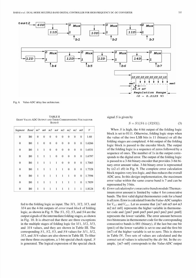
2) Design of Value-ADC delay line: The Value-ADC delay
line architecture based on piecewise linear characteristic
is shown in Fig. 6. Each delay block, D consists of two

8/11/2019 Dual-Mode Multiple-Band Digital Controller for High-Frequency DC–DC Converter
http://slidepdf.com/reader/full/dual-mode-multiple-band-digital-controller-for-high-frequency-dcdc-converter 4/15
BARAI et al.: DUAL-MODE MULTIPLE-BAND DIGITAL CONTROLLER FOR HIGH-FREQUENCY DC–DC CONVERTER 755
Fig. 3. Block diagram of MBDS delay line ADC.
Fig. 4. Timing waveforms for MBDS delay line ADC.
NOR gates. Mux denotes a multiplexer block and b7–b1
are connected to the control inputs of the multiplexer. The
Band-ADC output values (b7–b1) are used to select the
Fig. 5. Multiple overlapped band versus regulation window of MBDS delayline ADC.
multiplexers to scale the effective length for the Value-
ADC delay line. Value-ADC delay line length is adjusted
in such a way that the output of the Value-ADC reaches
8/11/2019 Dual-Mode Multiple-Band Digital Controller for High-Frequency DC–DC Converter
http://slidepdf.com/reader/full/dual-mode-multiple-band-digital-controller-for-high-frequency-dcdc-converter 5/15
756 IEEE TRANSACTIONS ON POWER ELECTRONICS, VOL. 24, NO. 3, MARCH 2009
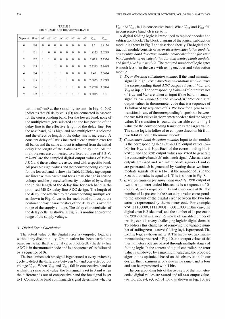
TABLE IEIGHT BANDS AND THE VOLTAGE RANGE
within m7–m0 at the sampling instant. In Fig. 6, 60D
indicates that 60 delay cells (D) are connected in cascadefor the corresponding band. For the lowest band, none of
the multiplexers gets selected and the last portion of the
delay line is the effective length of the delay line. For
the next band, b7 is high, and one multiplexer is selected
and the effective length of the delay line is increased. A
constant delay of 2 ns is incurred at each multiplexer for
all bands and the same amount is adjusted from the initial
delay line length of the Value-ADC delay line. All the
multiplexers are connected to a fixed voltage of 3.3 V.
m7–m0 are the sampled digital output values of Value-
ADC and these values are associated with a specific band.
All possible eight values and their corresponding voltagesfor the lowest band is shown in Table II. Delay tap outputs
are linear within each band for a small change in sensed
voltage, and the piecewise linearity is achieved by scaling
the initial length of the delay line for each band in the
proposed MBDS delay line ADC design. The length of
the delay line attached to the corresponding multiplexer,
as shown in Fig. 6, varies for each band to incorporate
nonlinear delay characteristics of the delay cells over the
range of the supply voltage. The delay characteristics of
the delay cells, as shown in Fig. 2, is nonlinear over the
range of the supply voltage.
A. Digital Error Calculation
The actual value of the digital error is computed logically
without any discontinuity. Optimization has been carried out
based on the fact that the digital value produced by the delay line
ADC is in thermometer code and is a sequence of 1s followed
by a sequence of 0s.
The band mismatch bm signal is generated at every switching
cycle to detect the difference between V re f and converter output
voltage V ou t . When V re f and V ou t fall in consecutive band or
within the same band value, the bm signal is set to 0 and when
the difference is out of consecutive band the bm signal is set
to 1. Consecutive band cb mismatch signal determines whether
V re f and V ou t fall in consecutive band. When V re f and V ou t fall
in consecutive band, cb is set to 1.
A digital folding logic is introduced to replace encoder and
subtraction block. The block diagram of the logical subtraction
module is shown in Fig. 7 and described shortly. The logical sub-
traction module consists of error direction calculation module,
consecutive band detection module, error calculation for sameband module, error calculation for consecutive bands module,
and final glue logic module. The required number of logic gates
is much less than the case with using encoder and subtraction
module.
1) Error direction calculation module: If the band mismatch
signal is high, error direction calculation module takes
the corresponding Band-ADC output values of V ou t and
V re f as input. The corresponding Value-ADC output values
of V ou t and V re f are taken as input if the band mismatch
signal is low. Band-ADC and Value-ADC produce digital
output values in thermometer code that is a sequence of
1s followed by sequence of 0s. We look for a zero to one
transition in any of the corresponding bit position betweenthe two 8-bit values in thermometer code to find the bigger
value. If a transition is found, the variable containing 1
value for the corresponding transition is the larger value.
The same logic is followed to compute direction bit from
two 8-bit values in thermometer code.
2) Consecutive band detection module: Input to this module
is the corresponding 8-bit Band-ADC output values (b7–
b0) for V ou t and V re f . Each of the corresponding bit is
XORed and the XOR output values are ORed to generate
the consecutive band (cb) mismatch signal. Alternate XOR
outputs are ORed and two intermediate signals i1 and i2
are generated. cb is generated by XORing these two inter-mediate signals. cb is set to 1 if the number of 1s in the
XOR output value is equal to 1. This is shown in Fig. 8.
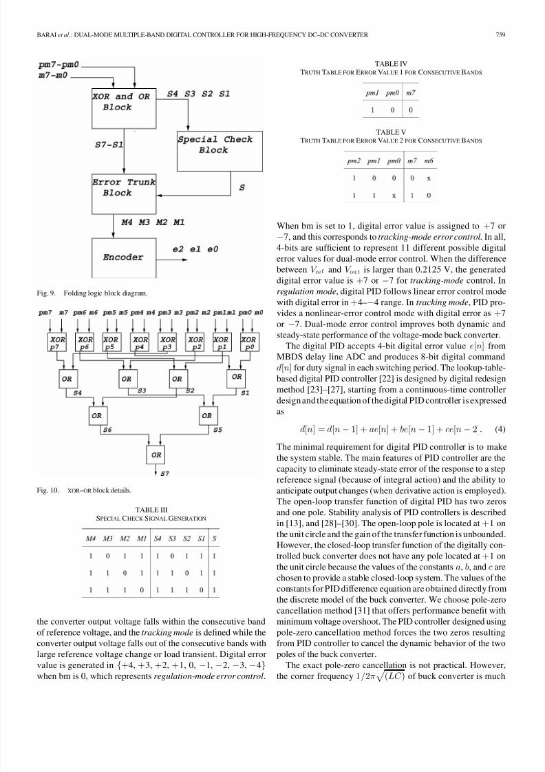
3) Error calculation for same band module: XOR output of
two thermometer-coded bitstreams is a sequence of 0s
(optional) and a sequence of 1s and a sequence of 0s. The
number of 1s present in the XOR output value corresponds
to the amount of the digital error between the two bit-
streams represented by thermometer code. For example,
XOR (11100000, 11111000) = 00011000. In this case, the
digital error is 2 (decimal) and the number of 1s present in
the XOR output is also 2. Removal of variable number of
trailing zeros is a very challenging logic in digital domain.
To address this challenge of removing the variable num-
ber of trailing zeros, a novel folding logic is proposed. The
folding logic is shown in Fig. 9. The hardware logic imple-
mentation is presented in Fig. 10. XOR output values of the
thermometer code are passed through multiple stages of
folding logic. In the context of digital controller, the error
value is windowed by a maximum value and the proposed
algorithm is optimized based on this observation. In our
design, the maximum error value in the same band is four
and can be represented with 4 bits.
The corresponding bits of the two sets of thermometer-
coded digital values are XORed and all XOR output values
( p7, p6, p5, p4, p3, p2, p1, p0), as shown in Fig. 10, are
8/11/2019 Dual-Mode Multiple-Band Digital Controller for High-Frequency DC–DC Converter
http://slidepdf.com/reader/full/dual-mode-multiple-band-digital-controller-for-high-frequency-dcdc-converter 6/15
BARAI et al.: DUAL-MODE MULTIPLE-BAND DIGITAL CONTROLLER FOR HIGH-FREQUENCY DC–DC CONVERTER 757
Fig. 6. Value-ADC delay line architecture.
TABLE IIEIGHT VALUE-ADC OUTPUT AND THEIR CORRESPONDING VOLTAGE FOR
BAND 0
fed to the folding logic as input. The M 1, M 2, M 3, and
M 4 are the 4-bit outputs of error trunk block of folding
logic, as shown in Fig. 9. The S 1, S 2, S 3, and S 4 are the
output signals of the intermediate folding stages, as shown
in Fig. 10. It is observed that there are three exceptions
in the multiple stages of folding logic for M 1, M 2, M 3,
and M 4 values, and they are shown in Table III. The
corresponding S 1, S 2, S 3, and S 4 values for M 1, M 2,
M 3, and M 4 values are also shown in Table III. To filter
out these three exceptions, a 1-bit special check signal, S
is generated. The logical expression of the special check
signal S is given by
S = S 1(S 4 ⊕ (S 2S 3)). (3)
When S is high, the 4-bit output of the folding logic
block is set to 0111. Otherwise, folding logic stops when
the value of the two LSB bits is 11 (binary) or all the
folding stages are completed. 4-bit output of the folding
logic block is passed to the encoder block. The outputof the folding logic is a sequence of zeros followed by a
sequence of ones. The number of 1s in the output corre-
sponds to the digital error. The output of the folding logic
is passed to a 3-bit binary encoder that provides 3-bit bi-
nary error amount value. 3-bit binary error is represented
by (e2 e1 e0) in Fig. 9. The complete error calculation
block requires very less logic, and thus reduces the overall
ADC area. In this design implementation, the maximum
error value within the same coarse band is 7 and can be
represented by 3 bits.
4) Error calculationfor consecutive bands module:Themax-
imum error amount is limited by value 4 for consecutive
bands. The first valid digital thermometer code for a band
is all zero. Error is calculated from the Value-ADC samples
for V re f and V ou t . Let us assume that {m7 m6 m5 m4 m3
m2 m1 m0} represents the higher variable in thermome-
ter code and {pm7 pm6 pm5 pm4 pm3 pm2 pm1 pm0}represents the lower variable. The error amount between
two bitstreams in thermometer code for the corresponding
consecutive bands is 001 (binary), if the last but one bit
(pm1) of the lower variable is set to one and the first bit
(m7) of the higher variable is set to zero. This is shown
in Table IV. Two sets of values are calculated and the
correct set of values is selected by the dir bit. In the ex-
ample, {m7–m0} corresponds to the Value-ADC output

8/11/2019 Dual-Mode Multiple-Band Digital Controller for High-Frequency DC–DC Converter
http://slidepdf.com/reader/full/dual-mode-multiple-band-digital-controller-for-high-frequency-dcdc-converter 7/15
758 IEEE TRANSACTIONS ON POWER ELECTRONICS, VOL. 24, NO. 3, MARCH 2009
Fig. 7. Proposed logical subtraction block diagram.
Fig. 8. Consecutive band detection block diagram.
for V re f and {pm7-pm0} corresponds to the Value-ADC
value for V ou t . The error amount is 010 (binary) for the
two conditions specified as follows.
a) First bit of the higher variable (m7) is set to 0, and
three LSB bits {pm2 pm1 pm0} of the lower variable
are 100.
b) TwoMSB bits (m7 m6) of the higher variable are set to
10, and three LSB {pm2 pm1 pm0} bits of the lower
variable to 110. This is also shown in Table V.
5) Final glue logic module: The MSB of the 4-bit error out-
put is the direction bit. The three LSB bits represent the
amount of error in binary notation. If bm is high and cb
is low, the amount of error is set to 111. This represents
tracking mode. In case of regulation mode, if bm is lowand cbis high, error amount is set to the output of the error
calculation for consecutive bands module. The amount of
error for consecutive bands is in the range (+4)–(−4). If
V ou t and V re f fall in the same band, bm is zero and the
error amount is set to the output of error calculation for
same band module.
III. DUAL-MODE ERROR CONTROL
Two operating modes are introduced for the digital PID
controller to achieve fast stable response for voltage-mode-
controlled buck converter. Regulation mode is defined while
8/11/2019 Dual-Mode Multiple-Band Digital Controller for High-Frequency DC–DC Converter
http://slidepdf.com/reader/full/dual-mode-multiple-band-digital-controller-for-high-frequency-dcdc-converter 8/15
BARAI et al.: DUAL-MODE MULTIPLE-BAND DIGITAL CONTROLLER FOR HIGH-FREQUENCY DC–DC CONVERTER 759
Fig. 9. Folding logic block diagram.
Fig. 10. XOR–OR block details.
TABLE IIISPECIAL CHECK SIGNAL GENERATION
the converter output voltage falls within the consecutive band
of reference voltage, and the tracking mode is defined while the
converter output voltage falls out of the consecutive bands with
large reference voltage change or load transient. Digital error
value is generated in {+4, +3, +2, +1, 0, −1, −2, −3, −4}
when bm is 0, which represents regulation-mode error control.
TABLE IVTRUTH TABLE FOR ERROR VALUE 1 FOR CONSECUTIVE BANDS
TABLE VTRUTH TABLE FOR ERROR VALUE 2 FOR CONSECUTIVE BANDS
When bm is set to 1, digital error value is assigned to +7 or
−7, and this corresponds to tracking-mode error control. In all,
4-bits are sufficient to represent 11 different possible digital
error values for dual-mode error control. When the difference
between V re f and V ou t is larger than 0.2125 V, the generateddigital error value is +7 or −7 for tracking-mode control. In
regulation mode, digital PID follows linear error control mode
with digital error in +4–−4 range. In tracking mode, PID pro-
vides a nonlinear-error control mode with digital error as +7
or −7. Dual-mode error control improves both dynamic and
steady-state performance of the voltage-mode buck converter.
The digital PID accepts 4-bit digital error value e[n] from
MBDS delay line ADC and produces 8-bit digital command
d[n] for duty signal in each switching period. The lookup-table-
based digital PID controller [22] is designed by digital redesign
method [23]–[27], starting from a continuous-time controller
design and the equation of the digital PID controller is expressed
as
d[n] = d[n− 1] + ae[n] + be[n− 1] + ce[n− 2]. (4)
The minimal requirement for digital PID controller is to make
the system stable. The main features of PID controller are the
capacity to eliminate steady-state error of the response to a step
reference signal (because of integral action) and the ability to
anticipate output changes (when derivative action is employed).
The open-loop transfer function of digital PID has two zeros
and one pole. Stability analysis of PID controllers is described
in [13], and [28]–[30]. The open-loop pole is located at +1 on
the unit circle and the gain of the transfer function is unbounded.
However, the closed-loop transfer function of the digitally con-
trolled buck converter does not have any pole located at +1 on
the unit circle because the values of the constants a, b, and c are
chosen to provide a stable closed-loop system. The values of the
constants for PID difference equation are obtained directly from
the discrete model of the buck converter. We choose pole-zero
cancellation method [31] that offers performance benefit with
minimum voltage overshoot. The PID controller designed using
pole-zero cancellation method forces the two zeros resulting
from PID controller to cancel the dynamic behavior of the two
poles of the buck converter.
The exact pole-zero cancellation is not practical. However,
the corner frequency 1/2π
(LC ) of buck converter is much

8/11/2019 Dual-Mode Multiple-Band Digital Controller for High-Frequency DC–DC Converter
http://slidepdf.com/reader/full/dual-mode-multiple-band-digital-controller-for-high-frequency-dcdc-converter 9/15
760 IEEE TRANSACTIONS ON POWER ELECTRONICS, VOL. 24, NO. 3, MARCH 2009
less than the PID controller sampling frequency (which equals
to switching frequency), and the effect of nonexact pole-zero
cancellation is not detrimental as the two frequencies are well
separated.The cancellation method provides an extremelystable
system with a very minimum voltage overshoot.
The values of the constants are a = 25.42; b = −48.62; and
c = 24.2. This set of a, b, and c values provides a stable close-loop system and improves dynamic performance of the system.
Smaller values of a, b, and c reduces external memory storage
requirement.
Digital PID controller is implemented using a lookup table
that stores precomputed products of ae[n], be[n−1], ce[n−2]
for a total of 11 different values of the error signal [+7, −7
and in the range of (+4)–(−4)] for each variable in an external
memory. The product values are rounded to the closest integer.
The highest value of the error signal is 7, and 9 bits are required
to store each signed b-product value. Each a-product and c-
product value takes 8 bits. Hence, 25 bits are required for storing
a-product, b-product, and c-product values in external memory
corresponding to each error value. A total of 275 bits of externalmemory is required to store precomputed product values for 11
possible error values.
PID uses an 8-MHz clock for processing the d[n] value com-
putation whereas the switching frequency of the converter is 1
MHz. A single memory block is used to store precomputed prod-
ucts of ae[n], be[n−1], and ce[n−2] and access these product
values to the external memory during actual computation. The
external memory is accessed three times per switching cycle of
1 µs. An index value 2-bit is used to identify external memory
access for a-product, b-product, and c-product values. In this
design, PID area is optimized and data from external memory
is accessed while computing d[n] values. We consider a uni-form 9-bit storage for all product values in external memory to
simplify the access logic.
IV. DESIGN IMPLEMENTATION AND RESULTS
Proposed digital controller architecture, as shown in Fig. 1, is
implemented on an experimental prototype. A prototype digital
controller experimental setup consists of Altera DE2 cyclone-II
field-programmable gate array (FPGA) platform, MBDS delay
line ADC fabricated with discrete components and flip-flops.
The closed-loop operation is tested with 1-W, 1-MHz, syn-
chronous buck converter with input voltage range 4–6 V and
output LC filter of 4.7 µH and 22 µF, respectively. Novel fold-ing logic, encoder, dual-mode error control, lookup-table-based
PID, and an 8-bit edge-triggered hybrid DPWM designs are
implemented on the Altera DE2 cyclone II FPGA. An 8-bit
edge-triggered hybrid DPWM design is implemented from our
previous work, as reported in [32].
A. Simulation Results
The feasibility of the proposed integrated digital controller
design presented in this paper is also implemented in a standard
0.5-µm CMOS technology [34]. The complete digital controller
design reduces chip area and power consumption while deliv-
ering very good dynamic performance by introducing MBDS
Fig. 11. Timing diagram for dual-stage ADC control signals.
delay line ADC, dual-mode error control PID, and an edge-
triggered hybrid DPWM. Each block of the digital controller is
designed based on HDL verilog code. Synopsis [33] synthesis
(Design Vision), timing verification (Prime Time), chip layout
(Astro), and postlayout chip simulation (Nanosim) tools are
used to implement the complete digital controller chip design in
0.5-µm CMOS technology library of National Semiconductor
[34]. Transistor-level postlayoutsimulationresults are shown for
the proposed digital controller in a closed-loop operation with
synchronous buck converter of 1-MHz switching frequency.
Active chip area of the proposed MBDS delay line ADC is
0.28 mm2
. Lookup-table-based PID takes 0.24 mm2
and edge-triggered hybrid DPWM occupies 0.07 mm2 on-chip area only.
The total silicon area of the complete digital controller is less
than 0.7 mm2 in 0.5-µm CMOS technology. The proposed de-
sign of ADC consumes average current of 66 µA at 3.3 V with
sampling frequency of 1 MHz. It reduces 33% on-chip area
compared to an equivalent 64-tap delay line ADC. The com-
plete digital controller consumes an average current of 92 µA.
The voltage-mode digital loop achieves tracking time of less
than 10 µs for 1-V step change of the reference voltage and
settling time of 20 µs.
Figs. 11–16 illustrate the results obtained from postlayout
simulation. Fig. 11 depicts timingsignals of theproposedMBDS
delay line ADC. Timing signals are generated as described in
Section II. Fig. 12 demonstrates the sampled output obtained
from Band-ADC . It is observed that the sampled output values
(b7–b2) change from low to high linearly with the increase in
converter output voltage. Linear characteristics and continuous
smooth tracking are achieved from multiple continuous band of
the proposed MBDS delay line ADC. In a closed-loop operation,
band value of V ou t tracks the band value of V re f of the proposed
integrated digital controller design.
Fig. 13 shows the closed-loop operation results during a step
change inV re f from 2.0 to 3.0 V. The corresponding digital error
output from MBDS delay line ADC is shown in Fig. 14. The
digital loop takes less than 10µs to track the 1-V step change and

8/11/2019 Dual-Mode Multiple-Band Digital Controller for High-Frequency DC–DC Converter
http://slidepdf.com/reader/full/dual-mode-multiple-band-digital-controller-for-high-frequency-dcdc-converter 10/15
BARAI et al.: DUAL-MODE MULTIPLE-BAND DIGITAL CONTROLLER FOR HIGH-FREQUENCY DC–DC CONVERTER 761
Fig. 12. Linear characteristics output of Band-ADC for V re f 2.7 V.
Fig. 13. Converter output voltage during reference voltage transient from 2 to
3 V.
Fig. 14. Error output from MBDS delay line ADC during reference voltagetransient from 2 to 3 V.
Fig. 15. Converter output voltage during load current transient from 220 to320 mA at V re f = 3.3 V.
settles within 20µs in steady state. This proves that the proposal
provides fast response to the change in reference voltage over a
wide range.
Fig. 15 depicts the load current transient from 220 to 320 mA
at regulated output voltage V ou t = 3.3 V. The corresponding
digital error output and supply voltage transient in MBDS delay
line ADC are shown in Fig. 16, where e3 is the direction bit, e2
is the MSB bit for error value, and e0 is the LSB bit for error

8/11/2019 Dual-Mode Multiple-Band Digital Controller for High-Frequency DC–DC Converter
http://slidepdf.com/reader/full/dual-mode-multiple-band-digital-controller-for-high-frequency-dcdc-converter 11/15
762 IEEE TRANSACTIONS ON POWER ELECTRONICS, VOL. 24, NO. 3, MARCH 2009
Fig. 16. Error output from MBDS delay line ADC during load transient from220 to 320 mA at V re f = 3.3 V.
Fig. 17. Timing signals for the proposed MBDS delay line ADC.
value. Postlayout simulation results verify that the proposed
digital controller provides fast load transient response.
B. Experimental Results
Closed-loop operation of the proposed multiple-band dual-
mode digital controller is also carried out in an experimental
setup. All the demonstrated postlayout simulation results are
validated experimentally over a wide output voltage range (1.6–
3.3 V). Figs. 17–26 demonstrate the experimental results.
Fig. 17 depicts the timing signals for MBDS delay line ADC
operation obtained from experimental setup. These generated
Fig. 18. Linear characteristics output of Band-ADC.
Fig. 19. Closed-loop operation in steady state. Ch1: regulated output voltage;Ch3: analog switch output; Ch2: gate drive signal to main switch.
signals match the timing requirements as described in this
proposal.
Fig. 18 demonstrates the sampled output obtained from Band-
ADC . It is observed that the sampled output values (b7–b2)
change from low to high linearly with the increase in converter
output voltage. Figs. 19 and 20 illustrate the closed-loop opera-
tion of the proposed digital controller in steady state for two dif-
ferent V re f values. These results prove that the proposal achieves
smooth steady-state output voltage regulation. The analog sup-
ply voltages (V re f , V ou t ) fed to the proposed MBDS delay line
are nearly equal to the corresponding phase of the analog switch
output voltage.

8/11/2019 Dual-Mode Multiple-Band Digital Controller for High-Frequency DC–DC Converter
http://slidepdf.com/reader/full/dual-mode-multiple-band-digital-controller-for-high-frequency-dcdc-converter 12/15
BARAI et al.: DUAL-MODE MULTIPLE-BAND DIGITAL CONTROLLER FOR HIGH-FREQUENCY DC–DC CONVERTER 763
Fig. 20. Closed-loop operation in steady state. Ch1: regulated output voltage;Ch3: analog switch output; Ch2: gate drive signal to main switch.
Fig. 21. Closed-loop operation from startup. Ch1: regulated output voltage;Ch3: analog switch output.
Fig. 22. Closed-loop operation during reference step change. Ch1: regulatedoutput voltage; Ch3: analog switch output; Ch2: instant of applied V re f .
Figs. 21 and22 demonstrate theconverter output voltage build
up from initial start and from an arbitrary instant of applied
V re f , respectively. Converter output voltage smoothly tracks the
applied reference voltages of 2.5 and 2.8 V within 20 and 28 µs,
respectively. These output values prove that multiple continuous
band switching is continuous in nature for the proposed MBDS
Fig. 23. Closed-loop operation during reference voltage change from 1.6 Vto 2. 0 V. Ch1: regulated output voltage; Ch2: instant of step change in V re f .
Fig. 24. 4-bit digital error output from the proposed MBDS delay line ADCCh1: e2-MSB of error; Ch2: e1; Ch3: e0-LSB of error; Ch4: e3-direction bit.
Fig. 25. Closed-loop operation during load transient from 315 to 630 mACh1: regulated output voltage; Ch4: instant of load transient.
delay line ADC. The introduction of the multiple-band concept
improves steady-state regulation over a wide regulated voltage
range.
Fig. 23 shows the closed-loop operation during a step change
in V re f from 1.6 to 2.0 V. The proposed digital loop achieves a
fast transition time of 6.4 µs for the voltage step change from

8/11/2019 Dual-Mode Multiple-Band Digital Controller for High-Frequency DC–DC Converter
http://slidepdf.com/reader/full/dual-mode-multiple-band-digital-controller-for-high-frequency-dcdc-converter 13/15
764 IEEE TRANSACTIONS ON POWER ELECTRONICS, VOL. 24, NO. 3, MARCH 2009
Fig. 26. Closed-loop operation during load transient from 660 to 330 mA.Ch2: regulated output voltage; Ch3: analog switch output; Ch4: instant of loadtransient.
Fig. 27. MBDS delay line ADC chip layout.
1.6 to 2.0 V. The corresponding digital error output obtained
from MBDS delay line ADC is shown in Fig. 24.Fig. 25 depicts the closed-loop operation during a load current
transient from 315 to 630 mA at regulated output voltage V ou t
= 3.15 V. Fig. 26 shows the closed-loop operation during a load
current transient from 660 to 330 mA at regulated output voltage
V ou t = 3.3 V. Theconverter regulated output voltage comes back
to steady-state value in less than 28 and 10 µs, respectively,
during load transients. These results prove the stability of the
proposed digital loop as well as fast load transient response.
The proposed controller achieves fast dynamic response and
better steady-state voltage regulation over a wide voltage range.
It is observed that the experimental results closely match the
simulation results for the proposed digital controller architec-
ture. Prototype digital controller experimental setup is shown in
Fig. 28. The on-chip layout for MBDS delay line ADC is shown
in Fig. 27. I/O pads are not included in the ADC chip layout.
Synopsys Astro tool is used for generating the chip layout.
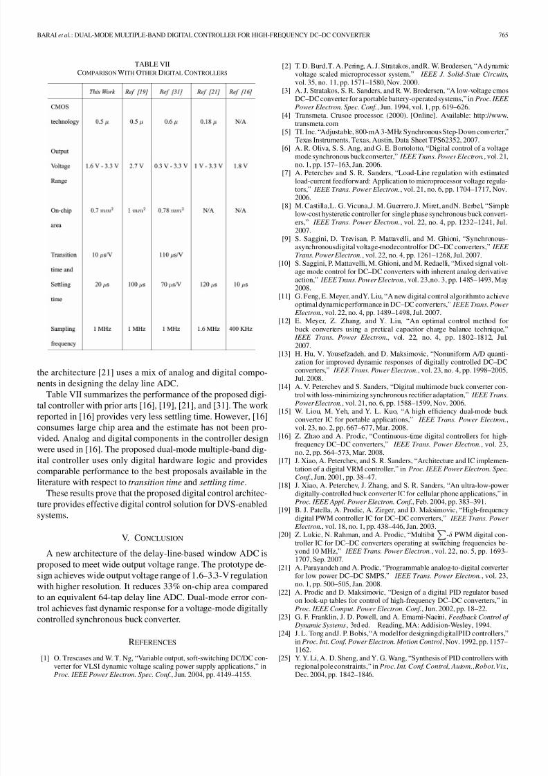
Table VI compares the performance of MBDS delay line
ADC architecture with the basic delay line ADC architecture
reported in [19], an extended delay line ADC that refers to 64-
tap ADC designed using the method described in [19] and [21].
The work [21] demonstrates closed-loop operation at 1.6-MHz
switching frequency. The area requirement of [21] is compa-
rable to the proposed MBDS delay line ADC, assuming linear
relationship between shrinking feature size as [21] implements
16-tap delay line ADC in 0.18-µs CMOS technology. However,
Fig. 28. Experimental setup with the proposed MBDS delay line ADC.
TABLE VIDELAYLINE ADC PERFORMANCE COMPARISON
8/11/2019 Dual-Mode Multiple-Band Digital Controller for High-Frequency DC–DC Converter
http://slidepdf.com/reader/full/dual-mode-multiple-band-digital-controller-for-high-frequency-dcdc-converter 14/15
BARAI et al.: DUAL-MODE MULTIPLE-BAND DIGITAL CONTROLLER FOR HIGH-FREQUENCY DC–DC CONVERTER 765
TABLE VIICOMPARISON WITH OTHER DIGITAL CONTROLLERS
the architecture [21] uses a mix of analog and digital compo-
nents in designing the delay line ADC.
Table VII summarizes the performance of the proposed digi-
tal controller with prior arts [16], [19], [21], and [31]. The work reported in [16] provides very less settling time. However, [16]
consumes large chip area and the estimate has not been pro-
vided. Analog and digital components in the controller design
were used in [16]. The proposed dual-mode multiple-band dig-
ital controller uses only digital hardware logic and provides
comparable performance to the best proposals available in the
literature with respect to transition time and settling time.
These results prove that the proposed digital control architec-
ture provides effective digital control solution for DVS-enabled
systems.
V. CONCLUSION
A new architecture of the delay-line-based window ADC is
proposed to meet wide output voltage range. The prototype de-
sign achieves wide output voltage range of 1.6–3.3-V regulation
with higher resolution. It reduces 33% on-chip area compared
to an equivalent 64-tap delay line ADC. Dual-mode error con-
trol achieves fast dynamic response for a voltage-mode digitally
controlled synchronous buck converter.
REFERENCES
[1] O. Trescases and W. T. Ng, “Variable output, soft-switching DC/DC con-verter for VLSI dynamic voltage scaling power supply applications,” inProc. IEEE Power Electron. Spec. Conf., Jun. 2004, pp. 4149–4155.
[2] T. D. Burd,T. A. Pering, A. J. Stratakos, andR. W. Brodersen, “A dynamicvoltage scaled microprocessor system,” IEEE J. Solid-State Circuits,vol. 35, no. 11, pp. 1571–1580, Nov. 2000.
[3] A. J. Stratakos, S. R. Sanders, and R. W. Brodersen, “A low-voltage cmosDC–DC converter for a portable battery-operated systems,” in Proc. IEEE
Power Electron. Spec. Conf., Jun. 1994, vol. 1, pp. 619–626.[4] Transmeta. Crusoe processor. (2000). [Online]. Available: http://www.
transmeta.com[5] TI. Inc. “Adjustable, 800-mA 3-MHz Synchronous Step-Down converter,”
Texas Instruments, Texas, Austin, Data Sheet TPS62352, 2007.[6] A. R. Oliva, S. S. Ang, and G. E. Bortolotto, “Digital control of a voltage
mode synchronous buck converter,” IEEE Trans. Power Electron., vol. 21,no. 1, pp. 157–163, Jan. 2006.
[7] A. Peterchev and S. R. Sanders, “Load-Line regulation with estimatedload-current feedforward: Application to microprocessor voltage regula-tors,” IEEE Trans. Power Electron., vol. 21, no. 6, pp. 1704–1717, Nov.2006.
[8] M. Castilla,L. G. Vicuna,J. M. Guerrero,J. Miret, andN. Berbel, “Simplelow-cost hysteretic controller for single phase synchronous buck convert-ers,” IEEE Trans. Power Electron., vol. 22, no. 4, pp. 1232–1241, Jul.2007.
[9] S. Saggini, D. Trevisan, P. Mattavelli, and M. Ghioni, “Synchronous–asynchronousdigital voltage-modecontrolfor DC–DC converters,” IEEE
Trans. Power Electron., vol. 22, no. 4, pp. 1261–1268, Jul. 2007.[10] S. Saggini, P. Mattavelli, M. Ghioni, and M. Redaelli, “Mixed signal volt-
age mode control for DC–DC converters with inherent analog derivativeaction,” IEEE Trans. Power Electron., vol. 23,no. 3, pp. 1485–1493, May2008.
[11] G. Feng, E. Meyer, andY. Liu, “A new digital control algorithmto achieveoptimal dynamic performance in DC–DC converters,” IEEE Trans. Power
Electron., vol. 22, no. 4, pp. 1489–1498, Jul. 2007.[12] E. Meyer, Z. Zhang, and Y. Liu, “An optimal control method for
buck converters using a prctical capacitor charge balance technique,” IEEE Trans. Power Electron., vol. 22, no. 4, pp. 1802–1812, Jul.2007.
[13] H. Hu, V. Yousefzadeh, and D. Maksimovic, “Nonuniform A/D quanti-zation for improved dynamic responses of digitally controlled DC–DCconverters,” IEEE Trans. Power Electron., vol. 23, no. 4, pp. 1998–2005,Jul. 2008.
[14] A. V. Peterchev and S. Sanders, “Digital multimode buck converter con-trol with loss-minimizing synchronous rectifier adaptation,” IEEE Trans.
Power Electron., vol. 21, no. 6, pp. 1588–1599, Nov. 2006.[15] W. Liou, M. Yeh, and Y. L. Kuo, “A high efficiency dual-mode buck
converter IC for portable applications,” IEEE Trans. Power Electron.,vol. 23, no. 2, pp. 667–677, Mar. 2008.
[16] Z. Zhao and A. Prodic, “Continuous-time digital controllers for high-frequency DC–DC converters,” IEEE Trans. Power Electron., vol. 23,no. 2, pp. 564–573, Mar. 2008.
[17] J. Xiao, A. Peterchev, and S. R. Sanders, “Architecture and IC implemen-tation of a digital VRM controller,” in Proc. IEEE Power Electron. Spec.
Conf., Jun. 2001, pp. 38–47.[18] J. Xiao, A. Peterchev, J. Zhang, and S. R. Sanders, “An ultra-low-power
digitally-controlled buck converter IC for cellular phone applications,” inProc. IEEE Appl. Power Electron. Conf., Feb. 2004, pp. 383–391.
[19] B. J. Patella, A. Prodic, A. Zirger, and D. Maksimovic, “High-frequencydigital PWM controller IC for DC–DC converters,” IEEE Trans. Power
Electron., vol. 18, no. 1, pp. 438–446, Jan. 2003.[20] Z. Lukic, N. Rahman, and A. Prodic, “Multibit
-δ PWM digital con-
troller IC for DC–DC converters operating at switching frequencies be-yond 10 MHz,” IEEE Trans. Power Electron., vol. 22, no. 5, pp. 1693–1707, Sep. 2007.
[21] A. Parayandeh and A. Prodic, “Programmable analog-to-digital converterfor low power DC–DC SMPS,” IEEE Trans. Power Electron., vol. 23,no. 1, pp. 500–505, Jan. 2008.
[22] A. Prodic and D. Maksimovic, “Design of a digital PID regulator basedon look-up tables for control of high-frequency DC–DC converters,” inProc. IEEE Comput. Power Electron. Conf., Jun. 2002, pp. 18–22.
[23] G. F. Franklin, J. D. Powell, and A. Emami-Naeini, Feedback Control of
Dynamic Systems, 3rd ed. Reading, MA: Addision-Wesley, 1994.[24] J. L. Tong andJ. P. Bobis,“A modelfor designingdigitalPID controllers,”
in Proc. Int. Conf. Power Electron. Motion Control, Nov. 1992, pp. 1157–1162.
[25] Y. Y. Li, A. D. Sheng, and Y. G. Wang, “Synthesis of PID controllers withregional pole constraints,” in Proc. Int. Conf. Control, Autom.,Robot.Vis.,Dec. 2004, pp. 1842–1846.

8/11/2019 Dual-Mode Multiple-Band Digital Controller for High-Frequency DC–DC Converter
http://slidepdf.com/reader/full/dual-mode-multiple-band-digital-controller-for-high-frequency-dcdc-converter 15/15
766 IEEE TRANSACTIONS ON POWER ELECTRONICS, VOL. 24, NO. 3, MARCH 2009
[26] J. C. Basilio and S. R. Matos, “Design of PI and PID controllers withtransient performance specification,” IEEE Trans. Educ., vol. 45, no. 4,pp. 364–370, Nov. 2002.
[27] L. Guo, J. Y. Hung, and R. M. Nelms, “Digital controller design for buck and boost converters using root locus techniques,” in Proc. IEEE Ind.
Electron. Conf., Nov. 2003, pp. 1864–1869.[28] O. Linlin, T. Youchun, G. Danying, and Z. Weidong, “Stability analysis
of PID controllers for integral processes with time delay,” in Proc. Amer.
Control Conf., Jun. 2005, pp. 4247–4252.[29] A. Karimi, D. Garcia, and R. Longchamp, “PID controller tuning using
Bode’s integrals,” IEEE Trans. Control Syst. Technol., vol. 11, no. 6,pp. 812–821, Nov. 2003.
[30] L. H. Keel and S. P. Bhattacharyya, “Stability margins and digital im-plementation of controllers,” in Proc. Amer. Con trol Conf., Jun. 1998,pp. 2852–2856.
[31] M. Y. Chui, W. Ki, and C. Tsui, “A programmable integrated digitalcontroller for switching converters with dual-band switching and complexpole-zero compensation,” IEEE J. Solid-State Circuits, vol. 40, no. 3,pp. 772–780, Mar. 2005.
[32] M. Barai, S. SenGupta, and J. Biswas, “Optimized design of a delay linebased analog to digital converter for digital power management applica-tions,” in Proc. IEEE Power Electron. Spec. Conf., Jun. 2008, pp. 1801–1807.
[33] Synopsys. (2007). Synopsys eda tools [Online]. Available: http://www.synopsys.com
[34] National Semiconductor. (2006). National semiconductor 0.5 µm cmoslibrary [Online]. Available: http://www.national.com
Mukti Barai receivedthe B.E.degree in electricalen-gineeringfrom Bengal Engineering College,CalcuttaUniversity, Kolkata, India, in 1992, and the M.Tech.degree in 1994 from the Indian Institute of Technol-ogy, Kharagpur, India, whereshe is currentlyworkingtoward the Ph.D. degree at the Department of Elec-trical Engineering.
From 1994 to 2000, she was a Senior Engineer(Design and Development) in the Electronics Divi-sion, Bharat Heavy Electricals Limited, Bengaluru,India. From 2002 to 2002, she was a Principal Soft-
ware Development Engineer at Alcatel Internetworking, Inc. From 2003 to2004, she was at ST Microelectronics Research Laboratory, Computer AidedDesign Laboratory (CADL), Indian Institute of Science (IISc), Bengaluru. Hercurrent research interests include power electronics converter and digital con-troller architecture for power management application ICs.
Sabyasachi Sengupta received the B.E. degreein electrical engineering from Calcutta University,Kolkata, India, in 1973, and the M.Tech. and Ph.D.degrees fromthe Indian Instituteof Technology(IIT),Kharagpur, India, in 1976, and 1998, respectively.
He wasa Professorin theDepartment of ElectricalEngineering, IIT, Kharagpur. In June 2008, he joinedWest Bengal University of Technology, Kolkata, asthe Vice Chancellor. He was involved in a numberof consultancy jobs with industrial houses and is apartner in a faculty entrepreneurial organization. His
current research interests include the fields of switch-mode power supplies,modeling, and simulation of electrical drives.
Prof. Sengupta is a Life Member of the System Society of India.
JayantaBiswas receivedthe B.E.degree in computerscience from Bengal Engineering College, Kolkata,India, in 1993, and the M.E. degree in system scienceand automation and the Ph.D. degree from the Indian
Institute of Science, Bengaluru, India, in 1995 and2005, respectively.
From January 1995 to 1998, he was with NCR,Dayton, OH. From January 1999 to November 2002,he was with Alcatel Internetworking, Calabasas, CA,where from May 2000 to November 2002, he wasthe Project Manager at Alcatel Internetworking ATM
(core and edge) switch software development effort, and he was also leading tenGIG software development effort. He is currently leading embeddedproduct de-velopment and research activity at CEM Solutions, Bengaluru, as the TechnicalDirector. His current research interests include digital controller architecture forpower management application ICs, virtual platform development, H.264 codecdevelopment, complex SoC design, edge synthesis, multicasting over mobile adhoc network (MANET), high-speed multicast switches, and secure multicastand application layer multicast for mobile entertainment applications.