dual 2-input positive-and gate (rev. l) - texas instruments
TRANSCRIPT
1
271A
1B1Y
5
6 32A
2B 2Y
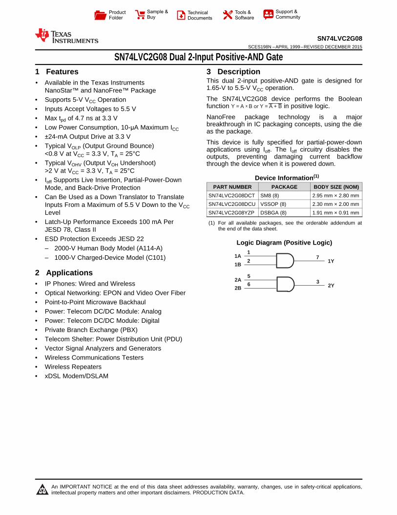
Y = A x B or Y = A + B
Product
Folder
Sample &Buy
Technical
Documents
Tools &
Software
Support &Community
SN74LVC2G08SCES198N –APRIL 1999–REVISED DECEMBER 2015
SN74LVC2G08 Dual 2-Input Positive-AND Gate1 Features 3 Description
This dual 2-input positive-AND gate is designed for1• Available in the Texas Instruments
1.65-V to 5.5-V VCC operation.NanoStar™ and NanoFree™ PackageThe SN74LVC2G08 device performs the Boolean• Supports 5-V VCC Operationfunction in positive logic.• Inputs Accept Voltages to 5.5 VNanoFree package technology is a major• Max tpd of 4.7 ns at 3.3 Vbreakthrough in IC packaging concepts, using the die• Low Power Consumption, 10-μA Maximum ICC as the package.
• ±24-mA Output Drive at 3.3 VThis device is fully specified for partial-power-down• Typical VOLP (Output Ground Bounce) applications using Ioff. The Ioff circuitry disables the<0.8 V at VCC = 3.3 V, TA = 25°C outputs, preventing damaging current backflow
• Typical VOHV (Output VOH Undershoot) through the device when it is powered down.>2 V at VCC = 3.3 V, TA = 25°C
Device Information(1)• Ioff Supports Live Insertion, Partial-Power-Down
PART NUMBER PACKAGE BODY SIZE (NOM)Mode, and Back-Drive ProtectionSN74LVC2G08DCT SM8 (8) 2.95 mm × 2.80 mm• Can Be Used as a Down Translator to TranslateSN74LVC2G08DCU VSSOP (8) 2.30 mm × 2.00 mmInputs From a Maximum of 5.5 V Down to the VCCSN74LVC2G08YZP DSBGA (8) 1.91 mm × 0.91 mmLevel
• Latch-Up Performance Exceeds 100 mA Per (1) For all available packages, see the orderable addendum atthe end of the data sheet.JESD 78, Class II
• ESD Protection Exceeds JESD 22 Logic Diagram (Positive Logic)– 2000-V Human Body Model (A114-A)– 1000-V Charged-Device Model (C101)
2 Applications• IP Phones: Wired and Wireless• Optical Networking: EPON and Video Over Fiber• Point-to-Point Microwave Backhaul• Power: Telecom DC/DC Module: Analog• Power: Telecom DC/DC Module: Digital• Private Branch Exchange (PBX)• Telecom Shelter: Power Distribution Unit (PDU)• Vector Signal Analyzers and Generators• Wireless Communications Testers• Wireless Repeaters• xDSL Modem/DSLAM
1
An IMPORTANT NOTICE at the end of this data sheet addresses availability, warranty, changes, use in safety-critical applications,intellectual property matters and other important disclaimers. PRODUCTION DATA.
SN74LVC2G08SCES198N –APRIL 1999–REVISED DECEMBER 2015 www.ti.com
Table of Contents8.2 Functional Block Diagram ......................................... 91 Features .................................................................. 18.3 Feature Description................................................... 92 Applications ........................................................... 18.4 Device Functional Modes.......................................... 93 Description ............................................................. 1
9 Application and Implementation ........................ 104 Revision History..................................................... 29.1 Application Information............................................ 105 Pin Configuration and Functions ......................... 39.2 Typical Application ................................................. 106 Specifications......................................................... 4
10 Power Supply Recommendations ..................... 116.1 Absolute Maximum Ratings ...................................... 411 Layout................................................................... 116.2 ESD Ratings ............................................................ 4
11.1 Layout Guidelines ................................................. 116.3 Recommended Operating Conditions ...................... 511.2 Layout Example .................................................... 116.4 Thermal Information .................................................. 5
12 Device and Documentation Support ................. 126.5 Electrical Characteristics........................................... 612.1 Community Resources.......................................... 126.6 Switching Characteristics .......................................... 612.2 Trademarks ........................................................... 126.7 Typical Characteristics .............................................. 712.3 Electrostatic Discharge Caution............................ 127 Parameter Measurement Information .................. 812.4 Glossary ................................................................ 128 Detailed Description .............................................. 9
13 Mechanical, Packaging, and Orderable8.1 Overview ................................................................... 9Information ........................................................... 12
4 Revision HistoryNOTE: Page numbers for previous revisions may differ from page numbers in the current version.
Changes from Revision M (April 2014) to Revision N Page
• Added Pin Configuration and Functions section, ESD Ratings and Thermal Information tables, Feature Descriptionsection, Device Functional Modes section, Application and Implementation section, Power SupplyRecommendations section, Layout section, Device and Documentation Support section, and Mechanical,Packaging, and Orderable Information section ..................................................................................................................... 1
2 Submit Documentation Feedback Copyright © 1999–2015, Texas Instruments Incorporated
Product Folder Links: SN74LVC2G08
GND 54 2A
3 6 2B2Y
2 7 1Y1B
8 VCC11A
3 6 2B2Y
81 VCC1A
5GND 4 2A
2 7 1Y1B
1 VCC81A
2 71B 1Y
3 62Y 2B
4 5GND 2A
SN74LVC2G08www.ti.com SCES198N –APRIL 1999–REVISED DECEMBER 2015
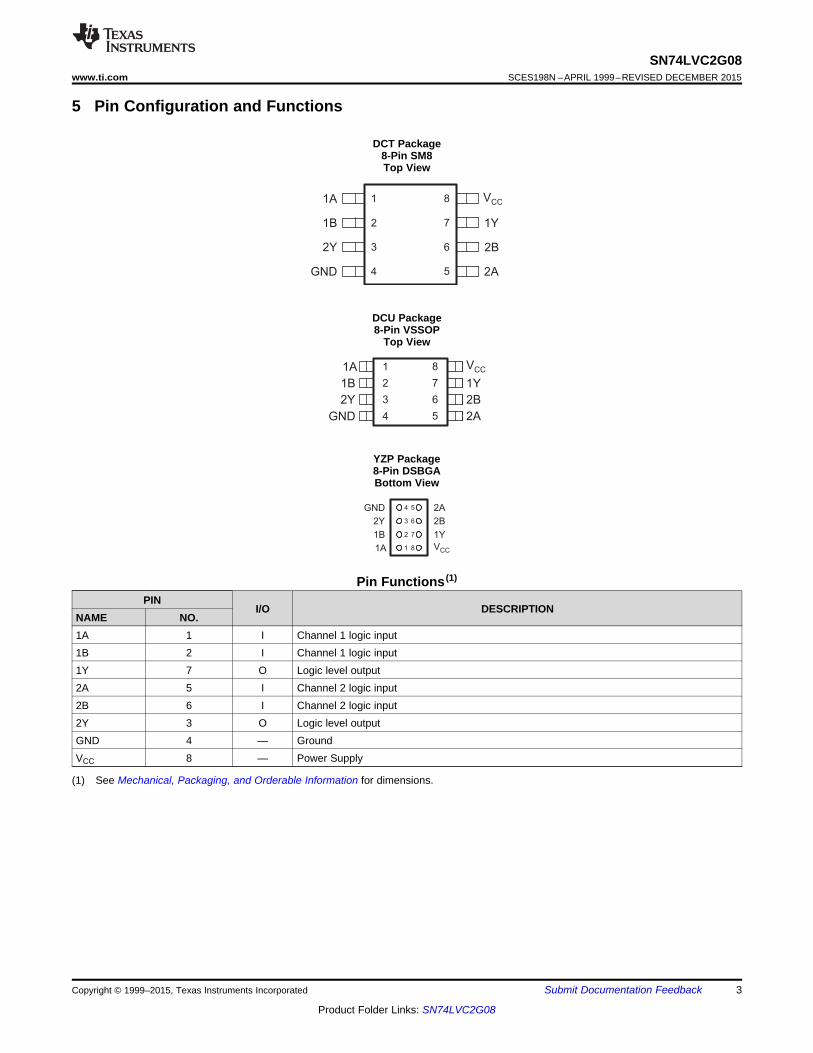
5 Pin Configuration and Functions
DCT Package8-Pin SM8Top View
DCU Package8-Pin VSSOP
Top View
YZP Package8-Pin DSBGABottom View
Pin Functions (1)
PINI/O DESCRIPTION
NAME NO.1A 1 I Channel 1 logic input1B 2 I Channel 1 logic input1Y 7 O Logic level output2A 5 I Channel 2 logic input2B 6 I Channel 2 logic input2Y 3 O Logic level outputGND 4 — GroundVCC 8 — Power Supply
(1) See Mechanical, Packaging, and Orderable Information for dimensions.
Copyright © 1999–2015, Texas Instruments Incorporated Submit Documentation Feedback 3
Product Folder Links: SN74LVC2G08
SN74LVC2G08SCES198N –APRIL 1999–REVISED DECEMBER 2015 www.ti.com
6 Specifications
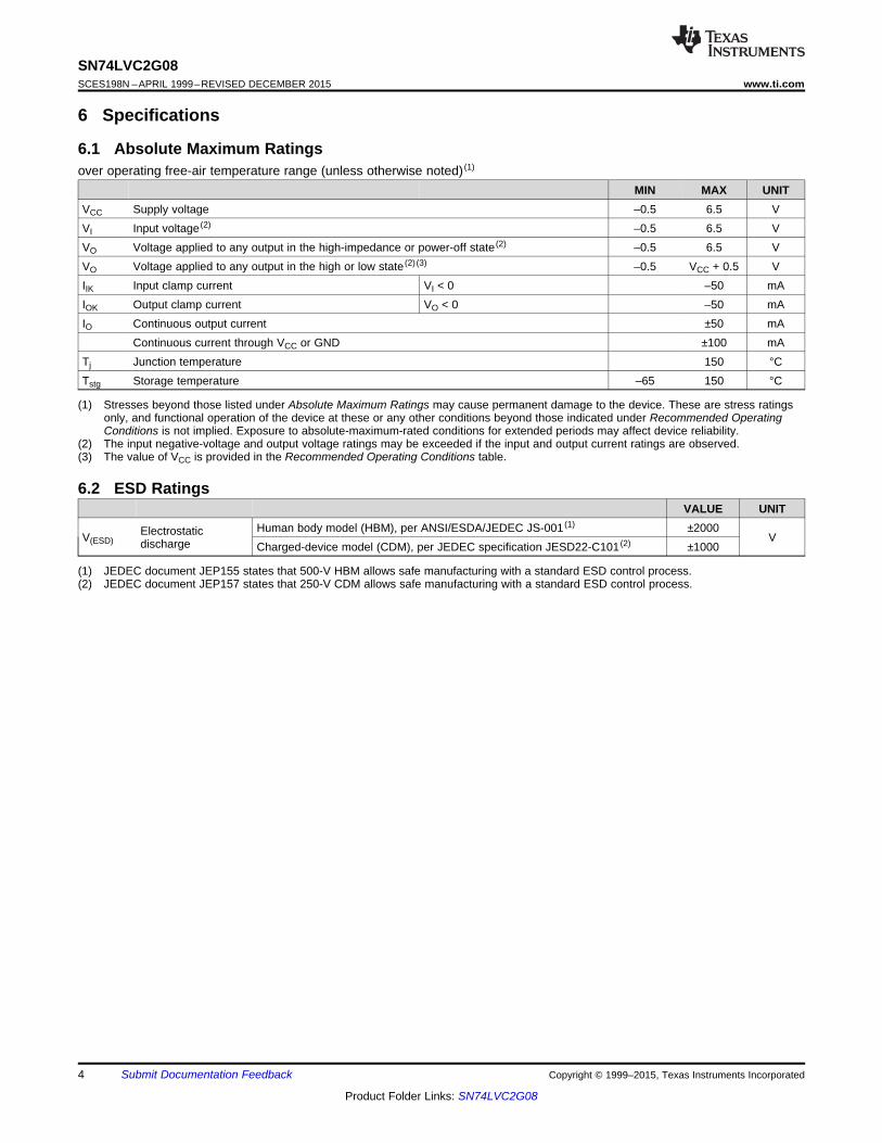
6.1 Absolute Maximum Ratingsover operating free-air temperature range (unless otherwise noted) (1)
MIN MAX UNITVCC Supply voltage –0.5 6.5 VVI Input voltage (2) –0.5 6.5 VVO Voltage applied to any output in the high-impedance or power-off state (2) –0.5 6.5 VVO Voltage applied to any output in the high or low state (2) (3) –0.5 VCC + 0.5 VIIK Input clamp current VI < 0 –50 mAIOK Output clamp current VO < 0 –50 mAIO Continuous output current ±50 mA
Continuous current through VCC or GND ±100 mATj Junction temperature 150 °CTstg Storage temperature –65 150 °C
(1) Stresses beyond those listed under Absolute Maximum Ratings may cause permanent damage to the device. These are stress ratingsonly, and functional operation of the device at these or any other conditions beyond those indicated under Recommended OperatingConditions is not implied. Exposure to absolute-maximum-rated conditions for extended periods may affect device reliability.
(2) The input negative-voltage and output voltage ratings may be exceeded if the input and output current ratings are observed.(3) The value of VCC is provided in the Recommended Operating Conditions table.
6.2 ESD RatingsVALUE UNIT
Human body model (HBM), per ANSI/ESDA/JEDEC JS-001 (1) ±2000ElectrostaticV(ESD) Vdischarge Charged-device model (CDM), per JEDEC specification JESD22-C101 (2) ±1000
(1) JEDEC document JEP155 states that 500-V HBM allows safe manufacturing with a standard ESD control process.(2) JEDEC document JEP157 states that 250-V CDM allows safe manufacturing with a standard ESD control process.
4 Submit Documentation Feedback Copyright © 1999–2015, Texas Instruments Incorporated
Product Folder Links: SN74LVC2G08
SN74LVC2G08www.ti.com SCES198N –APRIL 1999–REVISED DECEMBER 2015
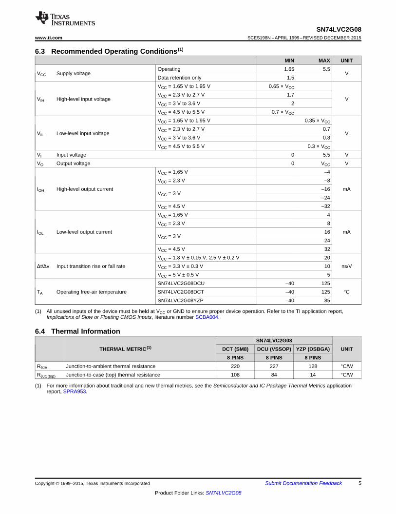
6.3 Recommended Operating Conditions (1)
MIN MAX UNITOperating 1.65 5.5
VCC Supply voltage VData retention only 1.5VCC = 1.65 V to 1.95 V 0.65 × VCC
VCC = 2.3 V to 2.7 V 1.7VIH High-level input voltage V
VCC = 3 V to 3.6 V 2VCC = 4.5 V to 5.5 V 0.7 × VCC
VCC = 1.65 V to 1.95 V 0.35 × VCC
VCC = 2.3 V to 2.7 V 0.7VIL Low-level input voltage V
VCC = 3 V to 3.6 V 0.8VCC = 4.5 V to 5.5 V 0.3 × VCC
VI Input voltage 0 5.5 VVO Output voltage 0 VCC V
VCC = 1.65 V –4VCC = 2.3 V –8
IOH High-level output current –16 mAVCC = 3 V
–24VCC = 4.5 V –32VCC = 1.65 V 4VCC = 2.3 V 8
IOL Low-level output current 16 mAVCC = 3 V
24VCC = 4.5 V 32VCC = 1.8 V ± 0.15 V, 2.5 V ± 0.2 V 20
Δt/Δv Input transition rise or fall rate VCC = 3.3 V ± 0.3 V 10 ns/VVCC = 5 V ± 0.5 V 5SN74LVC2G08DCU –40 125
TA Operating free-air temperature SN74LVC2G08DCT –40 125 °CSN74LVC2G08YZP –40 85
(1) All unused inputs of the device must be held at VCC or GND to ensure proper device operation. Refer to the TI application report,Implications of Slow or Floating CMOS Inputs, literature number SCBA004.
6.4 Thermal InformationSN74LVC2G08
THERMAL METRIC (1) DCT (SM8) DCU (VSSOP) YZP (DSBGA) UNIT8 PINS 8 PINS 8 PINS
RθJA Junction-to-ambient thermal resistance 220 227 128 °C/WRθJC(top) Junction-to-case (top) thermal resistance 108 84 14 °C/W
(1) For more information about traditional and new thermal metrics, see the Semiconductor and IC Package Thermal Metrics applicationreport, SPRA953.
Copyright © 1999–2015, Texas Instruments Incorporated Submit Documentation Feedback 5
Product Folder Links: SN74LVC2G08
SN74LVC2G08SCES198N –APRIL 1999–REVISED DECEMBER 2015 www.ti.com
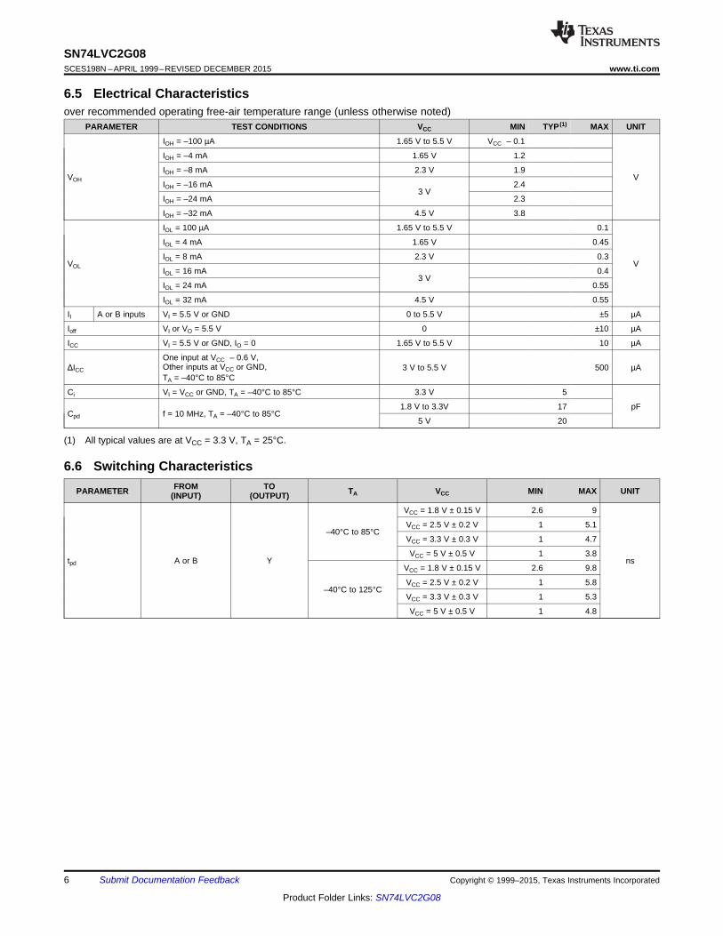
6.5 Electrical Characteristicsover recommended operating free-air temperature range (unless otherwise noted)
PARAMETER TEST CONDITIONS VCC MIN TYP (1) MAX UNIT
IOH = –100 µA 1.65 V to 5.5 V VCC – 0.1
IOH = –4 mA 1.65 V 1.2
IOH = –8 mA 2.3 V 1.9VOH V
IOH = –16 mA 2.43 V
IOH = –24 mA 2.3
IOH = –32 mA 4.5 V 3.8
IOL = 100 µA 1.65 V to 5.5 V 0.1
IOL = 4 mA 1.65 V 0.45
IOL = 8 mA 2.3 V 0.3VOL V
IOL = 16 mA 0.43 V
IOL = 24 mA 0.55
IOL = 32 mA 4.5 V 0.55
II A or B inputs VI = 5.5 V or GND 0 to 5.5 V ±5 µA
Ioff VI or VO = 5.5 V 0 ±10 µA
ICC VI = 5.5 V or GND, IO = 0 1.65 V to 5.5 V 10 µA
One input at VCC – 0.6 V,Other inputs at VCC or GND,ΔICC 3 V to 5.5 V 500 µATA = –40°C to 85°C
Ci VI = VCC or GND, TA = –40°C to 85°C 3.3 V 5
1.8 V to 3.3V 17 pFCpd f = 10 MHz, TA = –40°C to 85°C
5 V 20
(1) All typical values are at VCC = 3.3 V, TA = 25°C.
6.6 Switching CharacteristicsFROM TOPARAMETER TA VCC MIN MAX UNIT(INPUT) (OUTPUT)
VCC = 1.8 V ± 0.15 V 2.6 9
VCC = 2.5 V ± 0.2 V 1 5.1–40°C to 85°C
VCC = 3.3 V ± 0.3 V 1 4.7
VCC = 5 V ± 0.5 V 1 3.8tpd A or B Y ns
VCC = 1.8 V ± 0.15 V 2.6 9.8
VCC = 2.5 V ± 0.2 V 1 5.8–40°C to 125°C
VCC = 3.3 V ± 0.3 V 1 5.3
VCC = 5 V ± 0.5 V 1 4.8
6 Submit Documentation Feedback Copyright © 1999–2015, Texas Instruments Incorporated
Product Folder Links: SN74LVC2G08
Temperature - °C
TPD
- ns
-100 -50 0 50 100 1500
1
2
3
4
5
6
D001
TPD
Vcc - V
TPD
- ns
0 1 2 3 4 5 60
1
2
3
4
5
6
7
8
D002
TPD
SN74LVC2G08www.ti.com SCES198N –APRIL 1999–REVISED DECEMBER 2015
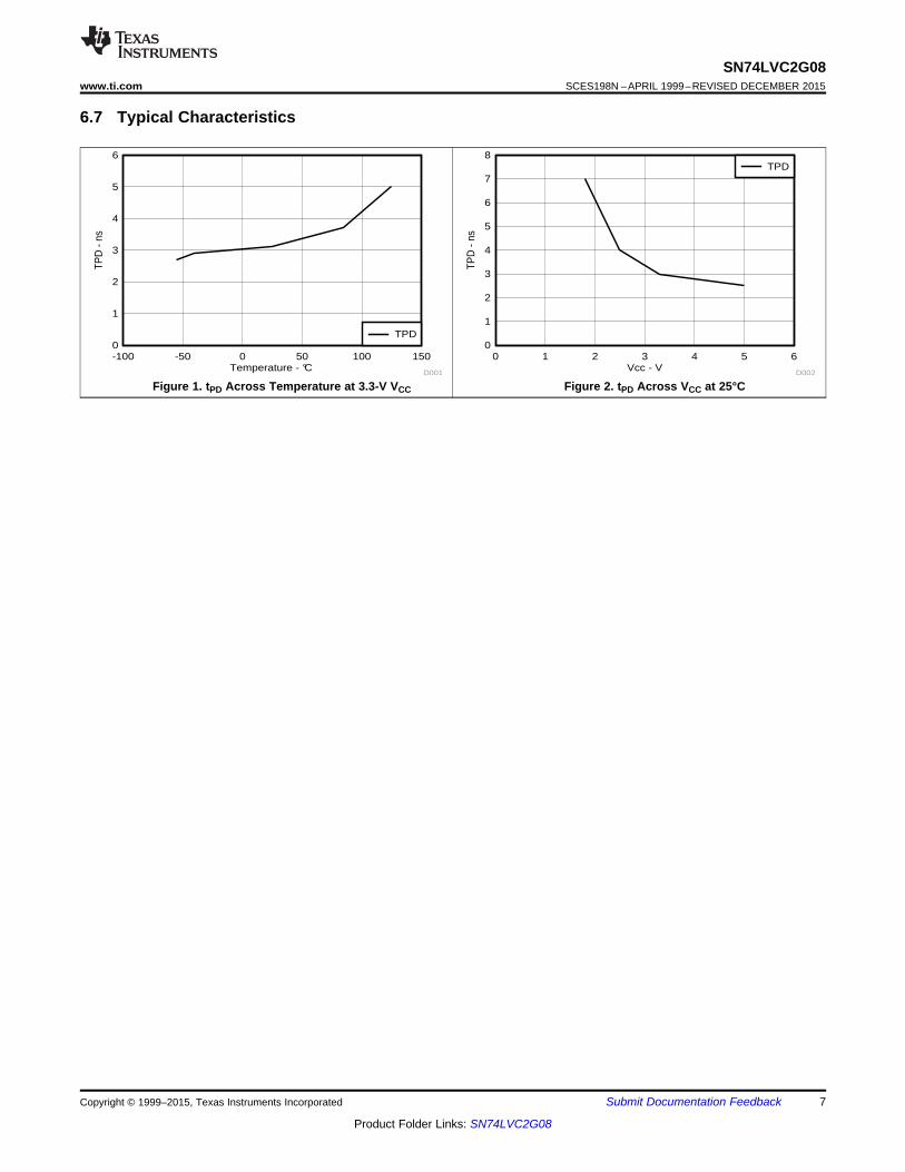
6.7 Typical Characteristics
Figure 1. tPD Across Temperature at 3.3-V VCC Figure 2. tPD Across VCC at 25°C
Copyright © 1999–2015, Texas Instruments Incorporated Submit Documentation Feedback 7
Product Folder Links: SN74LVC2G08
thtsu
From OutputUnder Test
C
(see Note A)L
LOAD CIRCUIT
S1
VLOAD
Open
GND
RL
Data Input
Timing Input
0 V
0 V0 V
tW
Input
0 VInput
OutputWaveform 1
S1 at V
(see Note B)LOAD
OutputWaveform 2
S1 at GND(see Note B)
VOL
VOH
0 V
»0 V
Output
Output
TEST S1
t /tPLH PHL Open
OutputControl
VM
VM VM
VM
VM
1.8 V 0.15 V±
2.5 V 0.2 V±
3.3 V 0.3 V±
5 V 0.5 V±
1 kW
500 W
500 W
500 W
VCC RL
2 × VCC
2 × VCC
6 V
2 × VCC
VLOAD CL
30 pF
30 pF
50 pF
50 pF
0.15 V
0.15 V
0.3 V
0.3 V
VD
3 V
VI
VCC/2
VCC/2
1.5 V
VCC/2
VM
£2 ns
£2 ns
£2.5 ns
£2.5 ns
INPUTS
RL
t /tr f
VCC
VCC
VCC
VLOADt /tPLZ PZL
GNDt /tPHZ PZH
VOLTAGE WAVEFORMSENABLE AND DISABLE TIMES
LOW- AND HIGH-LEVEL ENABLING
VOLTAGE WAVEFORMSPROPAGATION DELAY TIMES
INVERTING AND NONINVERTING OUTPUTS
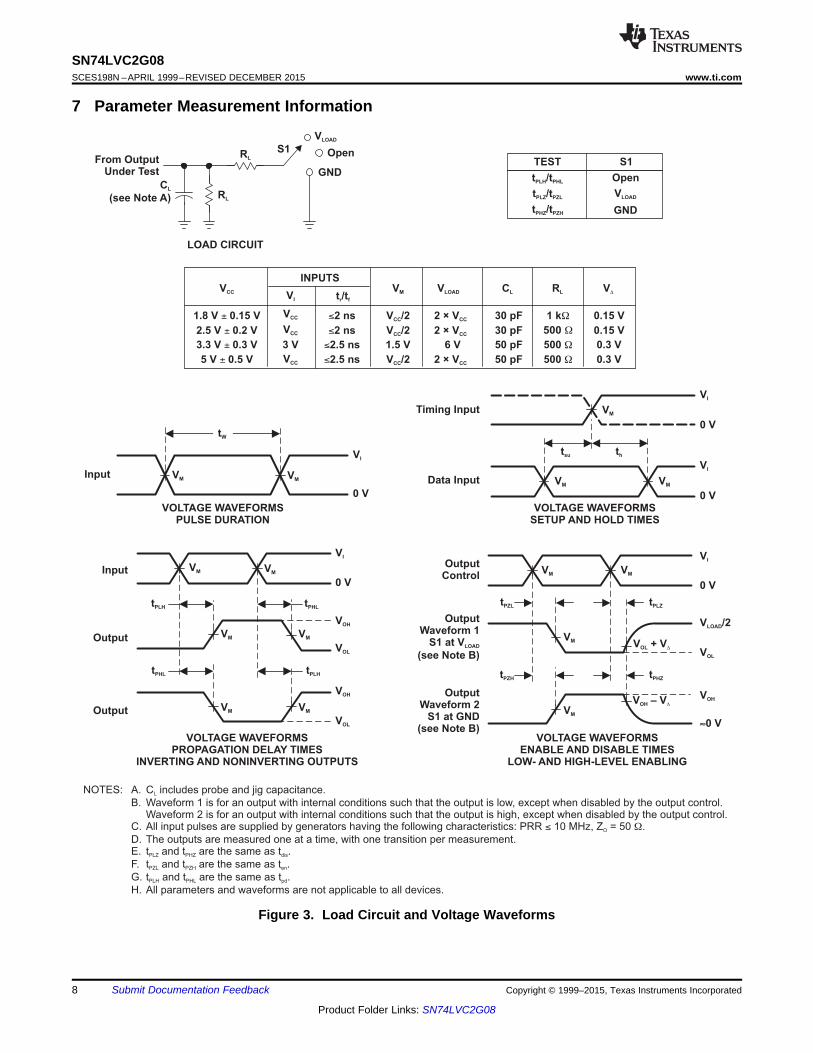
NOTES: A. C includes probe and jig capacitance.
B. Waveform 1 is for an output with internal conditions such that the output is low, except when disabled by the output control.Waveform 2 is for an output with internal conditions such that the output is high, except when disabled by the output control.
C. All input pulses are supplied by generators having the following characteristics: PRR 10 MHz, Z = 50 .
D. The outputs are measured one at a time, with one transition per measurement.E. t and t are the same as t .
F. t and t are the same as t .
G. t and t are the same as t .
H. All parameters and waveforms are not applicable to all devices.
L
O
PLZ PHZ dis
PZL PZH en
PLH PHL pd
£ W
VOLTAGE WAVEFORMSPULSE DURATION
VOLTAGE WAVEFORMSSETUP AND HOLD TIMES
VI
VI
VI
VM
VM
V /2LOAD
tPZL tPLZ
tPHZtPZH
V – VOH D
V + VOL D
VM
VM VM
VM
VOL
VOH
VI
VI
VOH
VOL
VM
VM
VM
VM
tPLH tPHL
tPLHtPHL
SN74LVC2G08SCES198N –APRIL 1999–REVISED DECEMBER 2015 www.ti.com
7 Parameter Measurement Information
Figure 3. Load Circuit and Voltage Waveforms
8 Submit Documentation Feedback Copyright © 1999–2015, Texas Instruments Incorporated
Product Folder Links: SN74LVC2G08
1
271A
1B1Y
5
6 32A
2B 2Y
SN74LVC2G08www.ti.com SCES198N –APRIL 1999–REVISED DECEMBER 2015
8 Detailed Description
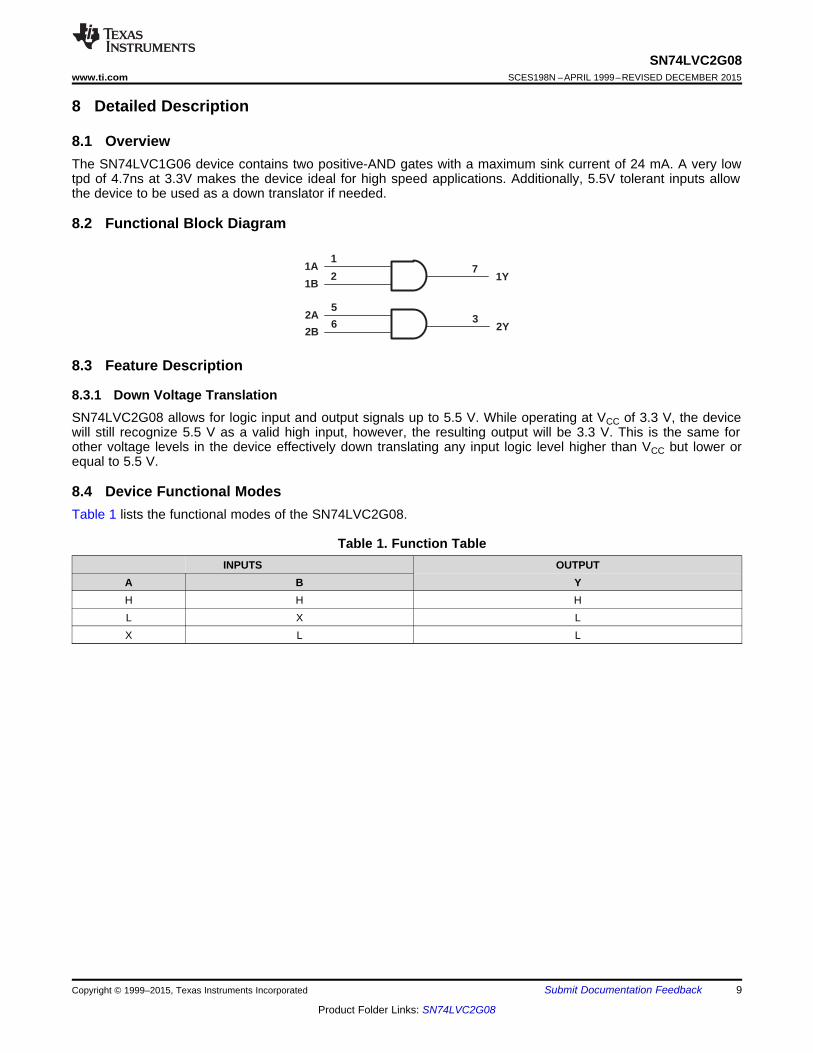
8.1 OverviewThe SN74LVC1G06 device contains two positive-AND gates with a maximum sink current of 24 mA. A very lowtpd of 4.7ns at 3.3V makes the device ideal for high speed applications. Additionally, 5.5V tolerant inputs allowthe device to be used as a down translator if needed.
8.2 Functional Block Diagram
8.3 Feature Description
8.3.1 Down Voltage TranslationSN74LVC2G08 allows for logic input and output signals up to 5.5 V. While operating at VCC of 3.3 V, the devicewill still recognize 5.5 V as a valid high input, however, the resulting output will be 3.3 V. This is the same forother voltage levels in the device effectively down translating any input logic level higher than VCC but lower orequal to 5.5 V.
8.4 Device Functional ModesTable 1 lists the functional modes of the SN74LVC2G08.
Table 1. Function TableINPUTS OUTPUT
A B YH H HL X LX L L
Copyright © 1999–2015, Texas Instruments Incorporated Submit Documentation Feedback 9
Product Folder Links: SN74LVC2G08
SN74LVC2G08SCES198N –APRIL 1999–REVISED DECEMBER 2015 www.ti.com
9 Application and Implementation
NOTEInformation in the following applications sections is not part of the TI componentspecification, and TI does not warrant its accuracy or completeness. TI’s customers areresponsible for determining suitability of components for their purposes. Customers shouldvalidate and test their design implementation to confirm system functionality.
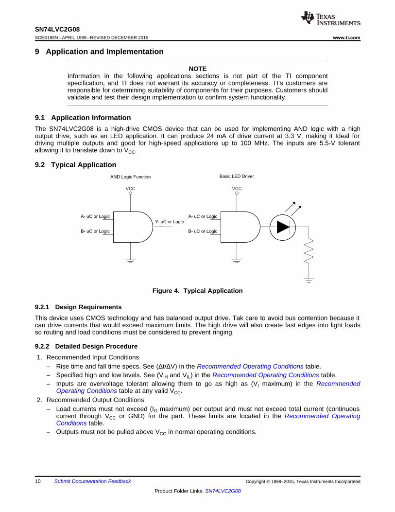
9.1 Application InformationThe SN74LVC2G08 is a high-drive CMOS device that can be used for implementing AND logic with a highoutput drive, such as an LED application. It can produce 24 mA of drive current at 3.3 V, making it Ideal fordriving multiple outputs and good for high-speed applications up to 100 MHz. The inputs are 5.5-V tolerantallowing it to translate down to VCC.
9.2 Typical Application
Figure 4. Typical Application
9.2.1 Design RequirementsThis device uses CMOS technology and has balanced output drive. Tak care to avoid bus contention because itcan drive currents that would exceed maximum limits. The high drive will also create fast edges into light loadsso routing and load conditions must be considered to prevent ringing.
9.2.2 Detailed Design Procedure1. Recommended Input Conditions
– Rise time and fall time specs. See (Δt/ΔV) in the Recommended Operating Conditions table.– Specified high and low levels. See (VIH and VIL) in the Recommended Operating Conditions table.– Inputs are overvoltage tolerant allowing them to go as high as (VI maximum) in the Recommended
Operating Conditions table at any valid VCC.2. Recommended Output Conditions
– Load currents must not exceed (IO maximum) per output and must not exceed total current (continuouscurrent through VCC or GND) for the part. These limits are located in the Recommended OperatingConditions table.
– Outputs must not be pulled above VCC in normal operating conditions.
10 Submit Documentation Feedback Copyright © 1999–2015, Texas Instruments Incorporated
Product Folder Links: SN74LVC2G08
VCC
Unused Input
Input
Output Output
Input
Unused Input
Frequency - MHz
Icc
- mA
-20 0 20 40 60 80-2
0
2
4
6
8
10
D003
Icc 1.8VIcc 2.5VIcc 3.3VIcc 5V
SN74LVC2G08www.ti.com SCES198N –APRIL 1999–REVISED DECEMBER 2015
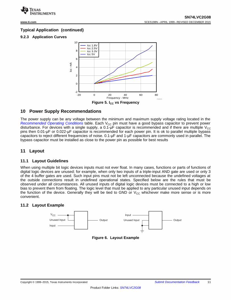
Typical Application (continued)9.2.3 Application Curves
Figure 5. ICC vs Frequency
10 Power Supply RecommendationsThe power supply can be any voltage between the minimum and maximum supply voltage rating located in theRecommended Operating Conditions table. Each VCC pin must have a good bypass capacitor to prevent powerdisturbance. For devices with a single supply, a 0.1-μF capacitor is recommended and if there are multiple VCCpins then 0.01-μF or 0.022-μF capacitor is recommended for each power pin. It is ok to parallel multiple bypasscapacitors to reject different frequencies of noise. 0.1-μF and 1-μF capacitors are commonly used in parallel. Thebypass capacitor must be installed as close to the power pin as possible for best results
11 Layout
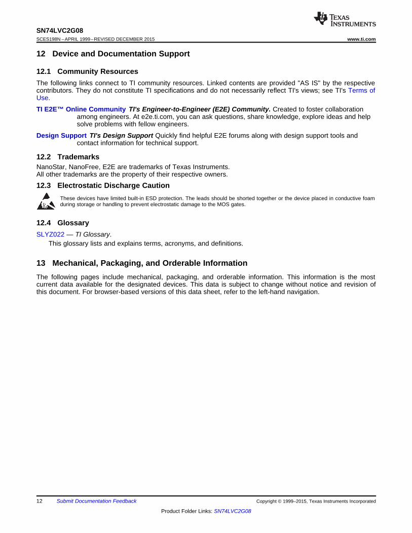
11.1 Layout GuidelinesWhen using multiple bit logic devices inputs must not ever float. In many cases, functions or parts of functions ofdigital logic devices are unused; for example, when only two inputs of a triple-input AND gate are used or only 3of the 4 buffer gates are used. Such input pins must not be left unconnected because the undefined voltages atthe outside connections result in undefined operational states. Specified below are the rules that must beobserved under all circumstances. All unused inputs of digital logic devices must be connected to a high or lowbias to prevent them from floating. The logic level that must be applied to any particular unused input depends onthe function of the device. Generally they will be tied to GND or VCC whichever make more sense or is moreconvenient.
11.2 Layout Example
Figure 6. Layout Example
Copyright © 1999–2015, Texas Instruments Incorporated Submit Documentation Feedback 11
Product Folder Links: SN74LVC2G08
SN74LVC2G08SCES198N –APRIL 1999–REVISED DECEMBER 2015 www.ti.com
12 Device and Documentation Support
12.1 Community ResourcesThe following links connect to TI community resources. Linked contents are provided "AS IS" by the respectivecontributors. They do not constitute TI specifications and do not necessarily reflect TI's views; see TI's Terms ofUse.
TI E2E™ Online Community TI's Engineer-to-Engineer (E2E) Community. Created to foster collaborationamong engineers. At e2e.ti.com, you can ask questions, share knowledge, explore ideas and helpsolve problems with fellow engineers.
Design Support TI's Design Support Quickly find helpful E2E forums along with design support tools andcontact information for technical support.
12.2 TrademarksNanoStar, NanoFree, E2E are trademarks of Texas Instruments.All other trademarks are the property of their respective owners.
12.3 Electrostatic Discharge CautionThese devices have limited built-in ESD protection. The leads should be shorted together or the device placed in conductive foamduring storage or handling to prevent electrostatic damage to the MOS gates.
12.4 GlossarySLYZ022 — TI Glossary.
This glossary lists and explains terms, acronyms, and definitions.
13 Mechanical, Packaging, and Orderable InformationThe following pages include mechanical, packaging, and orderable information. This information is the mostcurrent data available for the designated devices. This data is subject to change without notice and revision ofthis document. For browser-based versions of this data sheet, refer to the left-hand navigation.
12 Submit Documentation Feedback Copyright © 1999–2015, Texas Instruments Incorporated
Product Folder Links: SN74LVC2G08
PACKAGE OPTION ADDENDUM
www.ti.com 17-Aug-2015
Addendum-Page 1
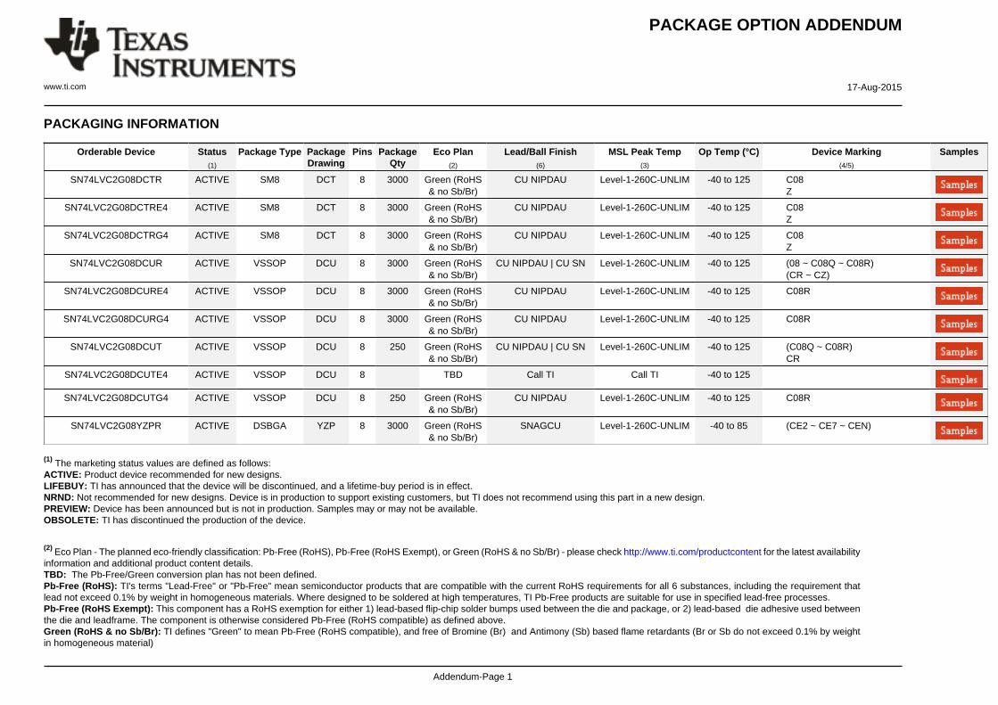
PACKAGING INFORMATION
Orderable Device Status(1)
Package Type PackageDrawing
Pins PackageQty
Eco Plan(2)
Lead/Ball Finish(6)
MSL Peak Temp(3)
Op Temp (°C) Device Marking(4/5)
Samples
SN74LVC2G08DCTR ACTIVE SM8 DCT 8 3000 Green (RoHS& no Sb/Br)
CU NIPDAU Level-1-260C-UNLIM -40 to 125 C08Z
SN74LVC2G08DCTRE4 ACTIVE SM8 DCT 8 3000 Green (RoHS& no Sb/Br)
CU NIPDAU Level-1-260C-UNLIM -40 to 125 C08Z
SN74LVC2G08DCTRG4 ACTIVE SM8 DCT 8 3000 Green (RoHS& no Sb/Br)
CU NIPDAU Level-1-260C-UNLIM -40 to 125 C08Z
SN74LVC2G08DCUR ACTIVE VSSOP DCU 8 3000 Green (RoHS& no Sb/Br)
CU NIPDAU | CU SN Level-1-260C-UNLIM -40 to 125 (08 ~ C08Q ~ C08R)(CR ~ CZ)
SN74LVC2G08DCURE4 ACTIVE VSSOP DCU 8 3000 Green (RoHS& no Sb/Br)
CU NIPDAU Level-1-260C-UNLIM -40 to 125 C08R
SN74LVC2G08DCURG4 ACTIVE VSSOP DCU 8 3000 Green (RoHS& no Sb/Br)
CU NIPDAU Level-1-260C-UNLIM -40 to 125 C08R
SN74LVC2G08DCUT ACTIVE VSSOP DCU 8 250 Green (RoHS& no Sb/Br)
CU NIPDAU | CU SN Level-1-260C-UNLIM -40 to 125 (C08Q ~ C08R)CR
SN74LVC2G08DCUTE4 ACTIVE VSSOP DCU 8 TBD Call TI Call TI -40 to 125
SN74LVC2G08DCUTG4 ACTIVE VSSOP DCU 8 250 Green (RoHS& no Sb/Br)
CU NIPDAU Level-1-260C-UNLIM -40 to 125 C08R
SN74LVC2G08YZPR ACTIVE DSBGA YZP 8 3000 Green (RoHS& no Sb/Br)
SNAGCU Level-1-260C-UNLIM -40 to 85 (CE2 ~ CE7 ~ CEN)
(1) The marketing status values are defined as follows:ACTIVE: Product device recommended for new designs.LIFEBUY: TI has announced that the device will be discontinued, and a lifetime-buy period is in effect.NRND: Not recommended for new designs. Device is in production to support existing customers, but TI does not recommend using this part in a new design.PREVIEW: Device has been announced but is not in production. Samples may or may not be available.OBSOLETE: TI has discontinued the production of the device.
(2) Eco Plan - The planned eco-friendly classification: Pb-Free (RoHS), Pb-Free (RoHS Exempt), or Green (RoHS & no Sb/Br) - please check http://www.ti.com/productcontent for the latest availabilityinformation and additional product content details.TBD: The Pb-Free/Green conversion plan has not been defined.Pb-Free (RoHS): TI's terms "Lead-Free" or "Pb-Free" mean semiconductor products that are compatible with the current RoHS requirements for all 6 substances, including the requirement thatlead not exceed 0.1% by weight in homogeneous materials. Where designed to be soldered at high temperatures, TI Pb-Free products are suitable for use in specified lead-free processes.Pb-Free (RoHS Exempt): This component has a RoHS exemption for either 1) lead-based flip-chip solder bumps used between the die and package, or 2) lead-based die adhesive used betweenthe die and leadframe. The component is otherwise considered Pb-Free (RoHS compatible) as defined above.Green (RoHS & no Sb/Br): TI defines "Green" to mean Pb-Free (RoHS compatible), and free of Bromine (Br) and Antimony (Sb) based flame retardants (Br or Sb do not exceed 0.1% by weightin homogeneous material)
PACKAGE OPTION ADDENDUM
www.ti.com 17-Aug-2015
Addendum-Page 2
(3) MSL, Peak Temp. - The Moisture Sensitivity Level rating according to the JEDEC industry standard classifications, and peak solder temperature.
(4) There may be additional marking, which relates to the logo, the lot trace code information, or the environmental category on the device.
(5) Multiple Device Markings will be inside parentheses. Only one Device Marking contained in parentheses and separated by a "~" will appear on a device. If a line is indented then it is a continuationof the previous line and the two combined represent the entire Device Marking for that device.
(6) Lead/Ball Finish - Orderable Devices may have multiple material finish options. Finish options are separated by a vertical ruled line. Lead/Ball Finish values may wrap to two lines if the finishvalue exceeds the maximum column width.
Important Information and Disclaimer:The information provided on this page represents TI's knowledge and belief as of the date that it is provided. TI bases its knowledge and belief on informationprovided by third parties, and makes no representation or warranty as to the accuracy of such information. Efforts are underway to better integrate information from third parties. TI has taken andcontinues to take reasonable steps to provide representative and accurate information but may not have conducted destructive testing or chemical analysis on incoming materials and chemicals.TI and TI suppliers consider certain information to be proprietary, and thus CAS numbers and other limited information may not be available for release.
In no event shall TI's liability arising out of such information exceed the total purchase price of the TI part(s) at issue in this document sold by TI to Customer on an annual basis.
OTHER QUALIFIED VERSIONS OF SN74LVC2G08 :
• Automotive: SN74LVC2G08-Q1
• Enhanced Product: SN74LVC2G08-EP
NOTE: Qualified Version Definitions:
• Automotive - Q100 devices qualified for high-reliability automotive applications targeting zero defects
• Enhanced Product - Supports Defense, Aerospace and Medical Applications
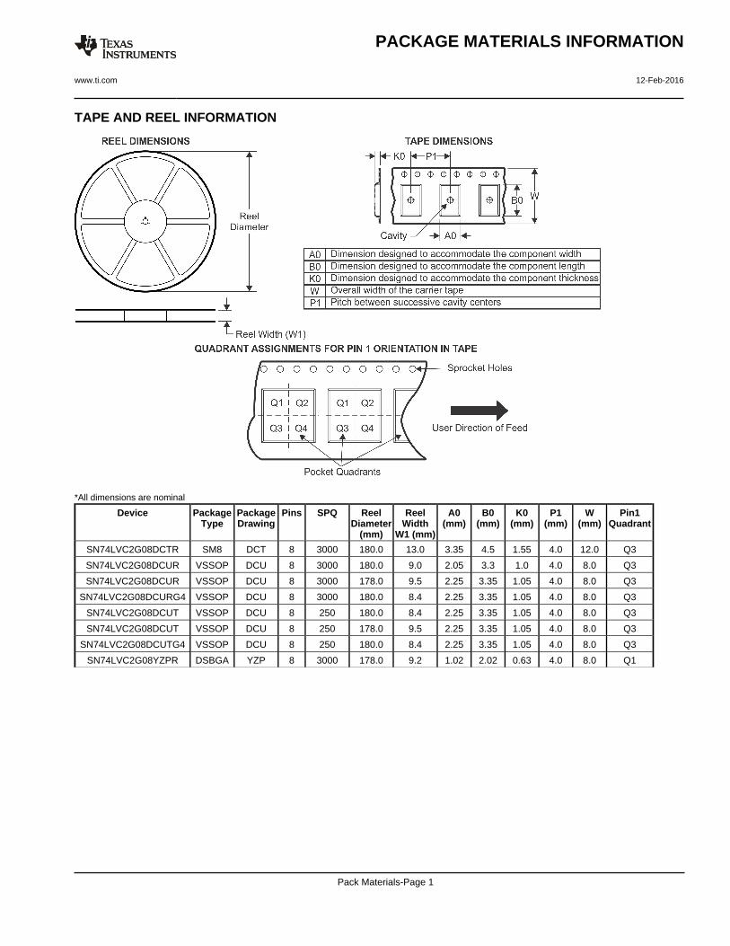
TAPE AND REEL INFORMATION
*All dimensions are nominal
Device PackageType
PackageDrawing
Pins SPQ ReelDiameter
(mm)
ReelWidth
W1 (mm)
A0(mm)
B0(mm)
K0(mm)
P1(mm)
W(mm)
Pin1Quadrant
SN74LVC2G08DCTR SM8 DCT 8 3000 180.0 13.0 3.35 4.5 1.55 4.0 12.0 Q3
SN74LVC2G08DCUR VSSOP DCU 8 3000 180.0 9.0 2.05 3.3 1.0 4.0 8.0 Q3
SN74LVC2G08DCUR VSSOP DCU 8 3000 178.0 9.5 2.25 3.35 1.05 4.0 8.0 Q3
SN74LVC2G08DCURG4 VSSOP DCU 8 3000 180.0 8.4 2.25 3.35 1.05 4.0 8.0 Q3
SN74LVC2G08DCUT VSSOP DCU 8 250 180.0 8.4 2.25 3.35 1.05 4.0 8.0 Q3
SN74LVC2G08DCUT VSSOP DCU 8 250 178.0 9.5 2.25 3.35 1.05 4.0 8.0 Q3
SN74LVC2G08DCUTG4 VSSOP DCU 8 250 180.0 8.4 2.25 3.35 1.05 4.0 8.0 Q3
SN74LVC2G08YZPR DSBGA YZP 8 3000 178.0 9.2 1.02 2.02 0.63 4.0 8.0 Q1
PACKAGE MATERIALS INFORMATION
www.ti.com 12-Feb-2016
Pack Materials-Page 1
*All dimensions are nominal
Device Package Type Package Drawing Pins SPQ Length (mm) Width (mm) Height (mm)
SN74LVC2G08DCTR SM8 DCT 8 3000 182.0 182.0 20.0
SN74LVC2G08DCUR VSSOP DCU 8 3000 182.0 182.0 20.0
SN74LVC2G08DCUR VSSOP DCU 8 3000 202.0 201.0 28.0
SN74LVC2G08DCURG4 VSSOP DCU 8 3000 202.0 201.0 28.0
SN74LVC2G08DCUT VSSOP DCU 8 250 202.0 201.0 28.0
SN74LVC2G08DCUT VSSOP DCU 8 250 202.0 201.0 28.0
SN74LVC2G08DCUTG4 VSSOP DCU 8 250 202.0 201.0 28.0
SN74LVC2G08YZPR DSBGA YZP 8 3000 220.0 220.0 35.0
PACKAGE MATERIALS INFORMATION
www.ti.com 12-Feb-2016
Pack Materials-Page 2
MECHANICAL DATA
MPDS049B – MAY 1999 – REVISED OCTOBER 2002
POST OFFICE BOX 655303 • DALLAS, TEXAS 75265
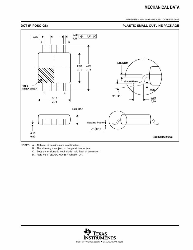
DCT (R-PDSO-G8) PLASTIC SMALL-OUTLINE PACKAGE
ÇÇÇÇÇÇÇÇÇÇÇÇÇÇÇÇÇÇÇÇ
0,600,20
0,25
0° – 8°
0,15 NOM
Gage Plane
4188781/C 09/02
4,25
5
0,300,15
2,903,752,70
8
4
3,152,75
1
0,100,00
1,30 MAX
Seating Plane
0,10
M0,130,65
PIN 1INDEX AREA
NOTES: A. All linear dimensions are in millimeters.B. This drawing is subject to change without notice.C. Body dimensions do not include mold flash or protrusionD. Falls within JEDEC MO-187 variation DA.
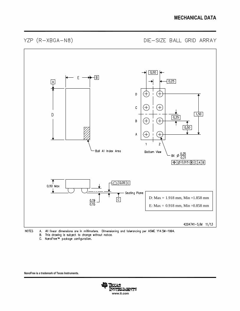
D: Max =
E: Max =
1.918 mm, Min =
0.918 mm, Min =
1.858 mm
0.858 mm
IMPORTANT NOTICE
Texas Instruments Incorporated and its subsidiaries (TI) reserve the right to make corrections, enhancements, improvements and otherchanges to its semiconductor products and services per JESD46, latest issue, and to discontinue any product or service per JESD48, latestissue. Buyers should obtain the latest relevant information before placing orders and should verify that such information is current andcomplete. All semiconductor products (also referred to herein as “components”) are sold subject to TI’s terms and conditions of salesupplied at the time of order acknowledgment.TI warrants performance of its components to the specifications applicable at the time of sale, in accordance with the warranty in TI’s termsand conditions of sale of semiconductor products. Testing and other quality control techniques are used to the extent TI deems necessaryto support this warranty. Except where mandated by applicable law, testing of all parameters of each component is not necessarilyperformed.TI assumes no liability for applications assistance or the design of Buyers’ products. Buyers are responsible for their products andapplications using TI components. To minimize the risks associated with Buyers’ products and applications, Buyers should provideadequate design and operating safeguards.TI does not warrant or represent that any license, either express or implied, is granted under any patent right, copyright, mask work right, orother intellectual property right relating to any combination, machine, or process in which TI components or services are used. Informationpublished by TI regarding third-party products or services does not constitute a license to use such products or services or a warranty orendorsement thereof. Use of such information may require a license from a third party under the patents or other intellectual property of thethird party, or a license from TI under the patents or other intellectual property of TI.Reproduction of significant portions of TI information in TI data books or data sheets is permissible only if reproduction is without alterationand is accompanied by all associated warranties, conditions, limitations, and notices. TI is not responsible or liable for such altereddocumentation. Information of third parties may be subject to additional restrictions.Resale of TI components or services with statements different from or beyond the parameters stated by TI for that component or servicevoids all express and any implied warranties for the associated TI component or service and is an unfair and deceptive business practice.TI is not responsible or liable for any such statements.Buyer acknowledges and agrees that it is solely responsible for compliance with all legal, regulatory and safety-related requirementsconcerning its products, and any use of TI components in its applications, notwithstanding any applications-related information or supportthat may be provided by TI. Buyer represents and agrees that it has all the necessary expertise to create and implement safeguards whichanticipate dangerous consequences of failures, monitor failures and their consequences, lessen the likelihood of failures that might causeharm and take appropriate remedial actions. Buyer will fully indemnify TI and its representatives against any damages arising out of the useof any TI components in safety-critical applications.In some cases, TI components may be promoted specifically to facilitate safety-related applications. With such components, TI’s goal is tohelp enable customers to design and create their own end-product solutions that meet applicable functional safety standards andrequirements. Nonetheless, such components are subject to these terms.No TI components are authorized for use in FDA Class III (or similar life-critical medical equipment) unless authorized officers of the partieshave executed a special agreement specifically governing such use.Only those TI components which TI has specifically designated as military grade or “enhanced plastic” are designed and intended for use inmilitary/aerospace applications or environments. Buyer acknowledges and agrees that any military or aerospace use of TI componentswhich have not been so designated is solely at the Buyer's risk, and that Buyer is solely responsible for compliance with all legal andregulatory requirements in connection with such use.TI has specifically designated certain components as meeting ISO/TS16949 requirements, mainly for automotive use. In any case of use ofnon-designated products, TI will not be responsible for any failure to meet ISO/TS16949.
Products ApplicationsAudio www.ti.com/audio Automotive and Transportation www.ti.com/automotiveAmplifiers amplifier.ti.com Communications and Telecom www.ti.com/communicationsData Converters dataconverter.ti.com Computers and Peripherals www.ti.com/computersDLP® Products www.dlp.com Consumer Electronics www.ti.com/consumer-appsDSP dsp.ti.com Energy and Lighting www.ti.com/energyClocks and Timers www.ti.com/clocks Industrial www.ti.com/industrialInterface interface.ti.com Medical www.ti.com/medicalLogic logic.ti.com Security www.ti.com/securityPower Mgmt power.ti.com Space, Avionics and Defense www.ti.com/space-avionics-defenseMicrocontrollers microcontroller.ti.com Video and Imaging www.ti.com/videoRFID www.ti-rfid.comOMAP Applications Processors www.ti.com/omap TI E2E Community e2e.ti.comWireless Connectivity www.ti.com/wirelessconnectivity
Mailing Address: Texas Instruments, Post Office Box 655303, Dallas, Texas 75265Copyright © 2016, Texas Instruments Incorporated