dspic33fj06gs101/x02 and dspic33fj16gsx02/x04
TRANSCRIPT

dsPIC33FJ06GS101/X02 anddsPIC33FJ16GSX02/X04
dsPIC33FJ06GS101/X02 and dsPIC33FJ16GSX02/X04 Family Silicon Errata and Data Sheet Clarification
The dsPIC33FJ06GS101/X02 and dsPIC33FJ16GSX02/X04 family devices that you have received conformfunctionally to the current Device Data Sheet(DS70000318G), except for the anomalies described inthis document.
The silicon issues discussed in the following pages arefor silicon revisions with the Device and Revision IDslisted in Table 1. The silicon issues are summarized inTable 2.
The errata described in this document will be addressedin future revisions of the dsPIC33FJ06GS101/X02 anddsPIC33FJ16GSX02/X04 silicon.
Data Sheet clarifications and corrections start on page 19,following the discussion of silicon issues.
The silicon revision level can be identified using thecurrent version of MPLAB® IDE and Microchip’sprogrammers, debuggers and emulation tools, whichare available at the Microchip corporate web site(www.microchip.com).
For example, to identify the silicon revision levelusing MPLAB IDE in conjunction with a hardwaredebugger:
1. Using the appropriate interface, connect thedevice to the hardware debugger.
2. Open an MPLAB IDE project.3. Configure the MPLAB IDE project for the
appropriate device and hardware debugger.4. Based on the version of MPLAB IDE you are
using, do one of the following:a) For MPLAB IDE 8, select Programmer >
Reconnect.b) For MPLAB X IDE, select Window >
Dashboard and click the Refresh DebugTool Status icon ( ).
5. Depending on the development tool used, thepart number and Device ID and Revision IDvalues appear in the Output window.
The Device and Revision ID values for the variousdsPIC33FJ06GS101/X02 and dsPIC33FJ16GSX02/X04silicon revisions are shown in Table 1.
Note: This document summarizes all siliconerrata issues from all revisions of silicon,previous as well as current. Only theissues indicated in the last column ofTable 2 apply to the current siliconrevision (A4).
Note: If you are unable to extract the siliconrevision level, please contact your localMicrochip sales office for assistance.
TABLE 1: SILICON DEVREV VALUES
Part Number Device ID(1)Revision ID for Silicon Revision(2)
A2 A3 A4
dsPIC33FJ06GS101 0x0C00
0x3002 0x3003 0x3004
dsPIC33FJ06GS102 0x0C01dsPIC33FJ06GS202 0x0C02dsPIC33FJ16GS402 0x0C04dsPIC33FJ16GS404 0x0C06dsPIC33FJ16GS502 0x0C03dsPIC33FJ16GS504 0x0C05Note 1: The Device and Revision IDs (DEVID and DEVREV) are located at the last two implemented addresses in
program memory.2: Refer to the “dsPIC33F/PIC24H Flash Programming Specification” (DS70152) for detailed information on
Device and Revision IDs for your specific device.
2009-2015 Microchip Technology Inc. DS80000439Q-page 1

dsPIC33FJ06GS101/X02 and dsPIC33FJ16GSX02/X04
TABLE 2: SILICON ISSUE SUMMARY
Module Feature Item Number Issue Summary
Affected Revisions(1)
A2 A3 A4
PWM Leading-Edge Blanking
1. Reading LEBCONx registers, as well as writing individual bits and bytes within these registers, does not work.
X X X
PWM Immediate Updates
2. PWM Immediate Update mode (IEU = 1) for the Master Duty Cycle register (MDC) is not functional.
X X X
PWM Status Bits 3. PWM Fault Status bits do not function if the associated PWM Fault interrupts are disabled.
X X X
PWM Clock 4. PWM output will exhibit jitter with some PWM clock divider settings.
X X X
PWM Faults 5. If the PWM is in Complementary, Redundant and Push-Pull mode and the Independent Time Base bit (ITB) is set, the Independent Fault mode may not work as expected for the PWMxL pin.
X X X
PWM Independent Time Base
6. The Independent Time Base PWM outputs may not be synchronized with the Master time base PWM outputs when both modes are used simultaneously.
X X X
PWM Latched Faults 7. In PWM Latched Fault mode, the PWM outputs may be latched on both the rising as well as the falling edge of the Fault signal regardless of the Fault input polarity selection (set with the FCLCONx<FLTPOL> bit setting).
X X X
PWM Faults 8. A bit write to the CLMOD bit (bit 8) in the FCLCONx register, or consecutive writes to the lower byte and higher byte of the FCLCONx register, causes all other bits of the high byte to be loaded with zeros.
X X X
PWM Sleep Mode 9. The PWM module fails to wake the CPU from Sleep mode on a PWM Fault event.
X X X
Comparator — 10. For slow input signals, the Comparator module may generate erroneous triggers/interrupts.
X X X
ADC Clock 11. Selecting the primary FRC (FVCO) as a clock source for the ADC module by setting the SLOWCLK bit (ADCON<12>) to the default setting of ‘0’, does not work.
X X X
Auxiliary Clock
Module Disable
12. When the PWMMD bit in the PMD1 register is set, the Auxiliary Clock to both the ADC and PWM modules is disabled.
X X X
Comparator Interrupts 13. Comparator interrupts are incorrectly generated when the High-Speed Analog Comparator is configured for an inverted polarity setting (CMPCONx<CMPPOL> = 1).
X X X
UART 4x Mode 14. When the UART is in 4x mode (BRGH = 1) and using two Stop bits (STSEL = 1), it may sample the first Stop bit instead of the second one.
X X X
UART IR Interface Operations
15. The 16x baud clock signal on the BCLK pin is present only when the module is transmitting.
X X X
I2C™ 10-Bit Addressing Mode
16. When the I2C™ module is configured for 10-bit addressing using the same address bits (A10 and A9) as other I2C devices, the A10 and A9 bits may not work as expected.
X X X
PWM ADC Conversion
17. The PWM module may fail to trigger a conversion on certain ADC pairs when the primary or secondary PWMx generator is selected as a trigger source.
X
Note 1: Only those issues indicated in the last column apply to the current silicon revision.
DS80000439Q-page 2 2009-2015 Microchip Technology Inc.

dsPIC33FJ06GS101/X02 and dsPIC33FJ16GSX02/X04
Core PGEC3/PGED3 Programming Pins
18. When using the PGEC3/PGED3 pins for device programming, the programming time may be slower as compared to other available PGECx/PGEDx pin pairs.
X X X
UART Break Character Generation
19. The UART module will not generate back-to-back Break characters.
X X X
PWM Current Limit 20. Cycle-by-cycle current-limit operation does not work when the PWM module is configured for Center-Aligned mode.
X X X
PWM Current Reset Mode
21. Current Reset mode does not work when the current-limit source (CLSRC) occurs during, and persists past, the assertive time interval of the PWM, and leading-edge blanking time is less than the PWM assertive time interval.
X X X
UART IrDA® Encoder/Decoder (8-bit Mode)
22. When the UART module is operating in 8-bit mode (PDSEL = 0x) and using the IrDA encoder/decoder (IREN = 1), the module incorrectly transmits a data payload of 80h as 00h.
X X X
UART UxE Interrupt 23. The UART error interrupt may not occur, or may occur at an incorrect time, if multiple errors occur during a short period of time.
X X X
I2C 10-Bit Addressing Mode
24. When the I2C™ module is configured as a 10-bit slave with an address of 0x102, the I2CxRCV register content for the lower address byte is 0x01 rather than 0x02.
X X X
I2C 10-Bit Addressing Mode
25. The 10-bit slave does not set the RBF flag or load the I2CxRCV register, on address match if the Least Significant bits (LSbs) of the address are the same as the 7-bit reserved addresses.
X X X
PSV Operations
Addressing Modes
26. An address error trap occurs in certain addressing modes when accessing the first four bytes of any PSV page.
X X X
Comparator Sleep Mode 27. The Comparator fails to wake the CPU from Sleep mode when the internal voltage reference is used.
X X X
PWM Independent Time Base
28. When updating the frequency on the fly, push-pull PWM outputs may not be synchronized with other PWM output modes.
X X X
Analog Comparator
Internal Band Gap Reference Voltage
29. The Internal Band Gap Reference Voltage (INTREF) for the analog comparator does not meet the stated accuracy specifications.
X X X
Auxiliary PLL Input Frequency
30. For extended temperature devices, the auxiliary PLL input frequency does not meet the published specification range.
X X X
ADC Current Consumption in Sleep Mode
31. If the ADC module is in an enabled state when the device enters Sleep mode, the power-down current (IPD) of the device may exceed the device data sheet specifications.
X X X
High-Speed PWM
PWM Module Enable
32. A glitch may be observed on the PWM pins when the PWM module is enabled after assignment of pin ownership to the PWM module.
X X X
Reserved — 33. — —
TABLE 2: SILICON ISSUE SUMMARY (CONTINUED)
Module Feature Item Number Issue Summary
Affected Revisions(1)
A2 A3 A4
Note 1: Only those issues indicated in the last column apply to the current silicon revision.
2009-2015 Microchip Technology Inc. DS80000439Q-page 3

dsPIC33FJ06GS101/X02 and dsPIC33FJ16GSX02/X04
PWM Duty Cycle Updates
34. When the PWM duty cycle update coincides with the PWM period rollover, the PWM output may be corrupted for one PWM period.
X X X
JTAG Active Pull-up 35. In JTAG mode, the TMS pin will not have an active pull-up as required by the JTAG specification.
X X X
SPI Framed Master Mode
36. When the SPI module is configured in Framed Master mode and the Frame Sync Pulse Edge Select bit (FRMDLY) is set to ‘1’, transmitting a word and then buffering another word in the SPIxBUF register before the transmission has completed, results in an incomplete transmission of the first data word.
X X X
Comparator Trigger Voltage Level
37. Output signal transitions occurring on the DACOUT pin (with DAC output disabled) can cause the Comparator trigger voltage level to change.
X X X
CPU Interrupt Disable
38. When a previous DISI instruction is active (i.e., the DISICNT register is non-zero), and the value of the DISICNT register is updated manually, the DISICNT register freezes and disables interrupts permanently.
X X X
CPU div.sd 39. When using the div.sd instruction, the overflow bit is not getting set when an overflow occurs.
X X X
UART TX Interrupt 40. A Transmit (TX) interrupt may occur before the data transmission is complete.
X X X
JTAG Flash Programming
41. JTAG Flash programming is not supported. X X X
PWM PWM Module Enable
42. If the PWM Clock Divider Select register, PTCON2, is not equal to zero, the PWM module may or may not initialize from an override state
X X X
PWM PWM SWAP 43. If the PWM is configured for Complimentary mode and the SWAP bit is enabled, the PWM outputs might operate as Redundant mode when the PHASE value is greater than the programmed dead-time (DTRx) value.
X X X
PWM Current-Limit Mode
44. A < 8-ns glitch may be observed on the PWM output pins when the Current-Limit event occurs.
X X X
PWM Immediate Update
45. Dead time is not asserted when PDCx is updated to cause an immediate transition on the PWMxH and PWMxL outputs.
X X X
ADC — 46. ADC measurement of INTREF may be zero under certain start-up conditions.
X X X
PWM Redundant/Push-Pull Output Mode
47. When the Immediate Update is disabled, changing the duty cycle value from a non-zero value to zero will produce a glitch pulse equal to 1 PWM clock.
X X X
PWM Master Time Base Mode
48. When the Immediate Update is disabled, certain changes to the PHASEx register may result in missing dead time.
X X X
PWM Trigger Compare Match
49. First PWM/ADC trigger event on TRIGx/STRIGx match may not occur under certain conditions.
X X X
I2C Slave Mode 50. Clock stretching may not occur when enabled. X X X
TABLE 2: SILICON ISSUE SUMMARY (CONTINUED)
Module Feature Item Number Issue Summary
Affected Revisions(1)
A2 A3 A4
Note 1: Only those issues indicated in the last column apply to the current silicon revision.
DS80000439Q-page 4 2009-2015 Microchip Technology Inc.

dsPIC33FJ06GS101/X02 and dsPIC33FJ16GSX02/X04
Silicon Errata Issues
1. Module: PWM
Reading LEBCONx registers, as well as writingindividual bits and bytes within these registersdoes not work.
Work aroundUse a Word write operation to modify LEBCONxregisters. For example, to set the PHR bit withinthe LEBCON1 register, use the following C code:
LEBCON1 = 0x8000
There is no work around for reading LEBCONxregisters.
Affected Silicon Revisions
2. Module: PWM
If PWM Immediate Update mode is selected(IUE = 1), and the PWM duty cycle is provided viathe Master Duty Cycle (MDC) register (MDCS = 1mode), the updates to the MDC register aresynchronized to the PWM time base instead of animmediate update (duty cycle will be updated onthe next PWM period).
Work aroundsWork around 1: Use the Enable Immediate Period Update mode(EIPU = 1) in conjunction with PWM ImmediateUpdate mode (IUE = 1). This will update the periodand duty cycle on an immediate basis.
Work around 2: Use individual duty cycle registers (PDCx) andPWM Immediate Update mode (IUE = 1) to updateindividual duty cycle registers on an immediatebasis.
Affected Silicon Revisions
3. Module: PWM
If PWM Fault interrupts are disabled (FLTIEN = 0or CLIEN = 0), then associated Status bits(FLTSTAT and CLSTAT) will not function.
Work aroundEnable PWM Fault interrupts (FLTIEN = 1,CLIEN = 1).
Affected Silicon Revisions
4. Module: PWM
The PWM output will exhibit jitter under thefollowing conditions:
When the PWM clock divider has the value of 1, 5or 6 (PTCON2<PCLKDIV> = 0b001, 0b101 or0b110), and the three Least Significant bits of thePWM Period Register (PTPER or PHASEx), DutyCycle Register (MDC or PDCx) or Phase Register(PHASEx) are non-zero.
Work aroundUse PWM clock dividers other than 1, 5 or 6.
Affected Silicon Revisions
Note: This document summarizes all siliconerrata issues from all revisions of silicon,previous as well as current. Only theissues indicated by the shaded column inthe following tables apply to the currentsilicon revision (A4).
A2 A3 A4
X X X
A2 A3 A4
X X X
A2 A3 A4
X X X
A2 A3 A4
X X X
2009-2015 Microchip Technology Inc. DS80000439Q-page 5

dsPIC33FJ06GS101/X02 and dsPIC33FJ16GSX02/X04
5. Module: PWM
When PWM module is operated inComplementary, Redundant and Push-pull outputmodes, with Independent Time Base (ITB = 1) andIndependent Fault mode (IFLTMOD = 1) enabled,the PWMxH and PWMxL outputs should beaffected by the Fault and Current-Limit events asfollows:
• PWMxH is affected by Current-Limit source (FCLCON<CLSRC>) and the Current-Limit should be reset at the end of the primary local time base.
• PWMxL is affected by Fault source (FCLCON<FLTSRC>) and the Fault should be reset at the end of the primary local time base.
On silicon revisions affected by this erratum, theCurrent-Limit event works correctly for the PWMxHpin. However, the Fault event is reset by thesecondary local time base although it is not used togenerate the time base value. As a result, the Faultevent on PWMxL pin may not work as expected.This erratum only applies to the cycle-by-cycle Faultmode (FLTMOD = 0b01).
Work aroundIf PWM is in Complementary, Redundant or Push-Pull mode and (ITB = 1), set SPHASEx to have thesame value as PHASEx. This will ensure that theFault event on the PWMxL pin is reset at the startof the new PWM period for cycle-by-cycleindependent Fault operation.
Affected Silicon Revisions
6. Module: PWM
The independent time base PWM outputs may notbe synchronized with the Master time base PWMoutputs when both modes are usedsimultaneously.
Work aroundTo synchronize the Independent PWM outputswith the Master time base PWM outputs, disablethe Immediate Update Enable bit (IUE = 0), ensurethat the three Least Significant bits of the periodare zero, and that the duty cycle is between 8 nsand the period minus 0x8.
This work around will not work if the frequency ofthe PWM module is being updated on the fly.
Affected Silicon Revisions
7. Module: PWM
In PWM Latched Fault mode, the PWM outputsmay be latched on both the rising as well as thefalling edge of the Fault signal, regardless of theFault input polarity selection (set with theFCLCONx<FLTPOL> bit setting).
Work aroundNone.
Affected Silicon Revisions
8. Module: PWM
A bit write to the CLMOD bit (bit 8) in theFCLCONx register or consecutive writes to thelower byte and higher byte of the FCLCONxregister, causes all other bits of the high byte to beloaded with zeros.
Work aroundUse Word writes for the FCLCONx register insteadof bit or byte writes.
Affected Silicon Revisions
A2 A3 A4
X X X
A2 A3 A4
X X X
A2 A3 A4
X X X
A2 A3 A4
X X X
DS80000439Q-page 6 2009-2015 Microchip Technology Inc.

dsPIC33FJ06GS101/X02 and dsPIC33FJ16GSX02/X04
9. Module: PWM
The PWM module fails to wake the CPU fromSleep mode on a PWM Fault event.
Work aroundUse the external interrupt pins to wake the CPUfrom Sleep mode.
Affected Silicon Revisions
10. Module: Comparator
If the slew rate of the Comparator input signal islower than 198 mV/µs, the Comparator modulegenerates erroneous triggers/interrupts.
Work aroundThe Slew rate of Comparator input signal must behigher than 198 mV/µs to avoid multiple triggers/interrupts.
Affected Silicon Revisions
11. Module: ADC
Selecting the primary FRC (FVCO) as a clocksource for the ADC module by setting theSLOWCLK bit (ADCON<12>) to the default settingof ‘0’, does not work.
Work aroundAlways set the SLOWCLK bit (ADCON<12>) to ‘1’,which selects the Auxiliary Clock (ACLK) as aclock source for the ADC. Use the Auxiliary ClockConfiguration registers to select the primary FRC(FVCO) as a source (if desired) or other clocksources as inputs. See Section 8.0 “OscillatorConfiguration” of the device data sheet(DS70000318G) for more information.
Affected Silicon Revisions
12. Module: Auxiliary Clock
When the PWMMD bit in the PMD1 register is set,the Auxiliary Clock to both the ADC and PWMmodules is disabled.
Work aroundTo disable the Auxiliary clock for the PWM modulebut not for the ADC module, set the individualPWM generator PMD bits in the PMD6 register.
Affected Silicon Revisions
13. Module: Comparator
The comparator interrupt should be generated ona rising edge of the comparator output. Whenusing the inverted polarity setting for the analogcomparator (CMPCONx<CMPPOL> = 1), theinterrupt should be generated when the analogvoltage at the comparator input falls below theprogrammable threshold determined by theCMPDAC register setting. However, with thissetting the interrupts may be generated regardlessof the state of the comparator.
Work aroundWhen using comparator interrupts, configure theexternal circuit to use the non-inverted polaritycomparator setting (CMPCONx<CMPPOL> = 0).
Affected Silicon Revisions
14. Module: UART
When the UART is in 4x mode (BRGH = 1) andusing two Stop bits (STSEL = 1), it may sample thefirst Stop bit instead of the second one.
This issue does not affect the other UARTconfigurations.
Work aroundUse the 16x baud rate option (BRGH = 0) andadjust the baud rate accordingly.
Affected Silicon Revisions
A2 A3 A4
X X X
A2 A3 A4
X X X
A2 A3 A4
X X X
A2 A3 A4
X X X
A2 A3 A4
X X X
A2 A3 A4
X X X
2009-2015 Microchip Technology Inc. DS80000439Q-page 7

dsPIC33FJ06GS101/X02 and dsPIC33FJ16GSX02/X04
15. Module: UART
When the UART is configured for IR interfaceoperations (UxMODE<9:8> = 11), the 16x baudclock signal on the BCLK pin is present only whenthe module is transmitting. The pin is idle at allother times.
Work aroundConfigure one of the output compare modules togenerate the required baud clock signal when theUART is receiving data or in an Idle state.
Affected Silicon Revisions
16. Module: I2C™
If there are two I2C devices on the bus, one ofthem is acting as the Master receiver and the otheras the Slave transmitter. If both devices areconfigured for 10-bit addressing mode, and havethe same value in the A10 and A9 bits of theiraddresses, then when the Slave select address issent from the Master, both the Master and SlaveAcknowledge it. When the Master sends out theread operation, both the Master and the Slaveenter into Read mode and both of them transmitthe data. The resultant data will be the ANDing ofthe two transmissions.
Work aroundIn all I2C devices, the addresses, as well as bits A10and A9, should be different.
Affected Silicon Revisions
17. Module: PWM
When the primary or secondary PWMx generatoris selected as a trigger source for ADC convertpairs 3, 4, 5 or 6 and the PWM module is runningat the maximum speed, the PWM module may failto trigger a conversion on these ADC pairs.
Work aroundsWork around 1: Configure the PWM module to trigger the ADCmodule per the following steps (see Example 1 forthe code used in this work around):
1. Enable the dual trigger mode bit (DTM) in theTRGCONx register.
2. Configure the TRIGx register to the desiredtrigger point.
3. Configure the STRIGx register to TRIGx + 0x8.4. Select the PWMx primary trigger as the ADC
trigger source for conversion.
If the PWM channel is configured for independentoutput mode and both channels are operating onthe same time base, the phase difference betweenthe two channels must be considered when settingthe STRIGx register. This work around will notwork for True Independent Time Base mode.
With this work around, the PWMx secondarytrigger should not be selected as the trigger sourcefor the ADC convert pair.
Work around 2: Configure the PWM Input Clock Prescaler bits(PCLKDIV) for divide by 2 or higher.
Work around 3: Utilize other available trigger sources, such assoftware or timer triggers, to initiate conversion onthe affected ADC convert pairs.
Affected Silicon Revisions
EXAMPLE 1: USING DUAL TRIGGER MODE
A2 A3 A4
X X X
A2 A3 A4
X X XA2 A3 A4
X
TRGCON1bits.DTM = 1; /* Dual trigger mode (DTM) and STRIG used in combination to generate */
/* ADCPx triggers */
TRIG1 = 1224; /* Configure desired trigger */
STRIG1 = 1232; /* STRIG1 should be configured for TRIG1 + 8 */
ADCPC2bits.TRGSRC5 = 0x4; /* PWM1 primary trigger selected as ADC trigger source for ADCP5*/
DS80000439Q-page 8 2009-2015 Microchip Technology Inc.

dsPIC33FJ06GS101/X02 and dsPIC33FJ16GSX02/X04
18. Module: Core
When using the PGEC3/PGED3 pins for deviceprogramming, the programming time may beslower as compared to other available PGECx/PGEDx pin pairs, because the Enhanced ICSP™programming algorithm cannot be executed onthis pin pair.
Refer to the “dsPIC33F/PIC24H Flash ProgrammingSpecification” (DS70152) for additional informationon this limitation.
Work aroundUse alternate PGECx/PGEDx programming pinpairs.
Affected Silicon Revisions
19. Module: UART
The UART module will not generate consecutiveBreak characters. Trying to perform a back-to-back Break character transmission will cause theUART module to transmit the dummy characterused to generate the first Break character insteadof transmitting the second Break character. Breakcharacters are generated correctly if they arefollowed by non-Break character transmission.
Work aroundNone.
Affected Silicon Revisions
20. Module: PWM
Cycle-by-cycle current-limit operation does notwork when the PWM module is configured forCenter-Aligned mode.
Work aroundNone.
Affected Silicon Revisions
21. Module: PWM
During normal operation, if Leading-EdgeBlanking (LEB) is triggered to start counting at arising edge of PWM and the PWM module has ablanking time period less than the PWM assertivetime (TON time), and the current-limit event occursduring the TON period and is still pending after theTON period is over, the current-limit event shouldbe ignored during TON time, but should berecognized after the TON time is over.
However, the device fails to recognize the current-limit event after TON time is over, when previouslydescribed conditions exist.
Work aroundInitialize the LEBCONx register as shown below,which specifies the LEB function for the (CLSRC)input to be triggered on the falling (trailing) edge ofPWM, and set the LEB delay to a minimum valueof 8 ns:
• PHF bit is set• CLLEBEN bit is set• LEB<9:3> bits are set to a minimum value of ‘1’
If the user application needs LEB to be triggered ata falling edge, make sure that the LEB delay is setfor more than the TON time.
Affected Silicon Revisions
22. Module: UART
When the UART is operating in 8-bit mode(PDSEL<1:0> = 0x) and using the IrDA® encoder/decoder (IREN = 1), the module incorrectlytransmits a data payload of 80h as 00h.
Work aroundNone.
Affected Silicon Revisions
A2 A3 A4
X X X
A2 A3 A4
X X X
A2 A3 A4
X X X
A2 A3 A4
X X X
A2 A3 A4
X X X
2009-2015 Microchip Technology Inc. DS80000439Q-page 9

dsPIC33FJ06GS101/X02 and dsPIC33FJ16GSX02/X04
23. Module: UART
The UART error interrupt may not occur, or mayoccur at an incorrect time, if multiple errors occurduring a short period of time.
Work aroundRead the error flags in the UxSTA registerwhenever a byte is received to verify the errorstatus. In most cases, these bits will be correct,even if the UART error interrupt fails to occur.
Affected Silicon Revisions
24. Module: I2C
When the I2C module is configured as a 10-bitslave with an address of 0x102, the I2CxRCVregister content for the lower address byte is 0x01,rather than 0x02; however, the moduleAcknowledges both address bytes.
Work aroundNone.
Affected Silicon Revisions
25. Module: I2C
In 10-Bit Addressing mode, some addressmatches do not set the RBF flag or load the I2CxReceive register, I2CxRCV, if the lower addressbyte matches the reserved addresses. Inparticular, these include all addresses with theform, ‘xx0000xx’ and ‘xx1111xxxx’, with thefollowing exceptions:
• ‘001111000x’• ‘011111001x’• ‘101111010x’• ‘111111011x’
Work aroundEnsure that the lower address byte in 10-BitAddressing mode does not match any 7-bitreserved addresses.
Affected Silicon Revisions
26. Module: PSV Operations
An address error trap occurs in certain addressingmodes when accessing the first four bytes of anPSV page. This occurs only when using thefollowing addressing modes:
• MOV.D
• Register Indirect Addressing (Word or Byte mode) with pre/post-decrement
Work aroundDo not perform PSV accesses to any of the firstfour bytes using the above addressing modes. Forapplications using the C language, MPLAB® C30Version 3.11 or higher, provides the followingcommand-line switch that implements a workaround for the erratum.-merrata=psv_trap
Refer to the readme.txt file in the MPLAB C30v3.11 toolsuite for further details.
Affected Silicon Revisions
27. Module: Comparator
The comparator fails to wake the CPU from Sleepmode when the internal voltage reference is used(i.e., the EXTREF bit is set to ‘0’).
Work aroundUse the external reference source by setting theEXTREF bit to ‘1’.
Affected Silicon Revisions
28. Module: PWM
When multiple PWM channels are operating inIndependent Time Base mode (ITB = 1) and thefrequency is being updated on the fly, PWM channelsconfigured for Push-Pull mode may not remainsynchronized with other PWM output modes.
Work aroundWhen multiple PWM channels are operating inIndependent Time Base mode, immediate updatesto the PWM module (IUE = 1) must be enabled forPWM channels to remain synchronized.
Affected Silicon Revisions
A2 A3 A4
X X X
A2 A3 A4
X X X
A2 A3 A4
X X X
A2 A3 A4
X X X
A2 A3 A4
X X X
A2 A3 A4
X X X
DS80000439Q-page 10 2009-2015 Microchip Technology Inc.

dsPIC33FJ06GS101/X02 and dsPIC33FJ16GSX02/X04
29. Module: Analog Comparator
The Internal Band Gap Reference Voltage(INTREF) for the analog comparator provides thereference to the analog comparator if the EXTREFbit (CMPCONx<5>) = 0 and the RANGE bit(CMPCONx<0>) = 0.The data sheet states thatthe INTREF voltage should be 1.2V nominal andwithin ±1%.
However, the internal band gap reference voltagedoes not meet the specification stated above. Forthe actual range of the INTREF voltage, refer tothe IVREF specification in the “ElectricalCharacteristics” chapter of the device datasheet.
Work aroundsTo avoid this issue, implement one of the followingtwo work arounds, depending on the applicationrequirements.
Work around 1:Use an external voltage reference for the AnalogComparator by setting the EXTREF bit(CMPCONx<5>) = 1 and providing an externalreference to the EXTREF pin.
Work around 2:Use the high-range setting for the internal referenceby setting the EXTREF bit (CMPCONx<5>) = 0 andthe RANGE bit (CMPCONx<0>) = 1. This settinguses AVDD/2 as the comparator reference voltage.
Affected Silicon Revisions
30. Module: Auxiliary PLL
For extended temperature devices (designatedwith the -E suffix in the device part number) withthe date code of 09XX, the auxiliary PLL inputfrequency does not meet the publishedspecification range at operating temperaturesabove +85ºC.
Work aroundUse the internal FRC oscillator as the input to theauxiliary PLL, or use the external oscillator with afrequency of 7.37 MHz.
Affected Silicon Revisions
A2 A3 A4
X X X
A2 A3 A4
X X X
2009-2015 Microchip Technology Inc. DS80000439Q-page 11

dsPIC33FJ06GS101/X02 and dsPIC33FJ16GSX02/X04
31. Module: ADC
If the ADC module is in an enabled state when thedevice enters Sleep mode as a result of executinga PWRSAV #0 instruction, the device power-downcurrent (IPD) may exceed the specifications listedin the device data sheet. This may happen even ifthe ADC module is disabled by clearing the ADONbit prior to entering Sleep mode.
Work aroundsWork around 1:In order to remain within the IPD specificationslisted in the device data sheet, the user softwaremust completely disable the ADC module bysetting the ADC Module Disable bit in thecorresponding Peripheral Module Disable x regis-ter (PMDx), prior to executing a PWRSAV #0instruction.
Work around 2:If the ADC module was previously initialized andenabled, before entering Sleep, execute the linesof code provided in Example 2.
EXAMPLE 2:
Affected Silicon Revisions
Note: The ADC module must be reinitialized bythe user application before resuming ADCoperation.
Note: Unlike Work around 1, the userapplication does not need to reinitializethe ADC module; however, it is necessaryto re-enable the ADC module by settingthe ADON bit after waking from Sleep.
AD1CON1bits.ADON = 0; //Disable the ADC module
__asm__ volatile ("REPEAT #50"); //Wait 50 TCY
__asm__ volatile ("NOP"); //Repeat NOP 51 times
Sleep(); // Execute PWRSAV #0 and go to Sleep
A2 A3 A4
X X X
DS80000439Q-page 12 2009-2015 Microchip Technology Inc.

dsPIC33FJ06GS101/X02 and dsPIC33FJ16GSX02/X04
32. Module: High-Speed PWM
The PENH and PENL bits in the IOCONx registerare used to assign ownership of the pins to eitherthe PWM module or the GPIO module. The correctprocedure to configure the PWM module is toassign pin ownership to the PWM module and thenenabling it using the PTEN bit in the PTCONregister.
If the PWM module is enabled using the abovesequence, then a glitch may be observed on thePWM pins before actual switching of the PWMoutputs begins. This glitch may cause momentaryturn-on of power MOSFETs that are driven by thePWM pins and may cause damage to theapplication hardware.
Work aroundFollow the given sequence to avoid any glitchesfrom appearing on the PWM outputs at the time ofenabling.
1. Configure the respective PWM pins to digitalinputs using the TRISx registers. This step willput the PWM pins in a high-impedance state.The PWM outputs must be maintained in a safestate by using pull-up or pull-down resistors.
2. Assign pin ownership to the GPIO module byconfiguring IOCONx<PENH> = 0 andIOCONx<PENL> = 0.
3. Specify the PWM override state to the desiredsafe state for the PWM pins using theOVRDAT<1:0> bit field in the IOCONx register.
4. Override the PWM outputs bysetting IOCONx<OVRENH> = 1 andIOCONx<OVRENL> = 1.
5. Enable the PWM module by settingPTCON<PTEN> = 1.
6. Remove the PWM overrides bymaking IOCONx<OVRENH> = 0 andIOCONx<OVRENL> = 0.
7. Ensure a delay of at least one full PWM cycle.8. Assign pin ownership to the PWM module
by setting IOCONx<PENH> = 1 andIOCONx<PENL> = 1.
The code in Example 3 illustrates the use of thiswork around.
Affected Silicon Revisions
EXAMPLE 3: CONFIGURE PWM MODULE TO PREVENT GLITCHES ON PWM1H AND PWM1L PINS AT THE TIME OF ENABLING
A2 A3 A4
X X X
TRISAbits.TRISA4 = 1; // Configure PWM1H/RA4 as digital input
// Ensure output is in safe state using pull-up or
// pull-down resistors
TRISAbits.TRISA3 = 1; // Configure PWM1L/RA3 as digital input
// Ensure output is in safe state using pull-up or
// pull-down resistors
IOCON1bits.PENH = 0; // Assign pin ownership of PWM1H/RA4 to GPIO module
IOCON1bits.PENL = 0; // Assign pin ownership of PWM1L/RA3 to GPIO module
IOCON1bits.OVRDAT = 0; // Configure override state of the PWM outputs to
// desired safe state.
IOCON1bits.OVRENH = 1; // Override PWM1H output
IOCON1bits.OVRENL = 1; // Override PWM1L output
PTCONbits.PTEN = 1; // Enable PWM module
IOCON1bits.OVRENH = 0; // Remove override for PWM1H output
IOCON1bits.OVRENL = 0; // Remove override for PWM1L output
Delay(x); // Introduce a delay greater than one full PWM cycle
IOCON1bits.PENH = 1; // Assign pin ownership of PWM1H/RA4 to PWM module
IOCON1bits.PENL = 1; // Assign pin ownership of PWM1L/RA3 to PWM module
2009-2015 Microchip Technology Inc. DS80000439Q-page 13

dsPIC33FJ06GS101/X02 and dsPIC33FJ16GSX02/X04
33. Module: Reserved
The issue in a previous version of the documentwas removed.
34. Module: PWM
The High-Speed PWM provides a feature toupdate the PWM duty cycle at any time during thePWM period. The new duty cycle should takeeffect:
• On the next PWM period when immediate duty cycle updates are disabled (PWMCONx<IUE> = 0).
• On the same PWM period when immediate duty cycle updates are enabled (PWMCONx<IUE> = 1).
However, when the immediate duty cycle updatesare disabled and the duty cycle update coincideswith a PWM period roll-over, the PWM output maybe corrupted and exhibit a 100% duty cycle for onePWM period. The new duty cycle value will takeeffect on the next PWM period.
Work aroundEnable immediate duty cycle updates byconfiguring PWMCONx<IUE> = 1.
Affected Silicon Revisions
35. Module: JTAG
In JTAG mode, the TMS pin will not have an activepull-up as required by the JTAG specification.Instead, the pull-up function will be enabled on theTCK pin.
Work aroundAn external pull-up resistor can be connected tothe TMS pin to ensure that the signal does notenter a tri-state condition when in JTAG mode.
There is no work around for the wrongly enabledpull-up function on the TCK pin.
Affected Silicon Revisions
36. Module: SPI
When the SPI module is configured in FramedMaster mode and the Frame Sync Pulse EdgeSelect bit (FRMDLY) is set to ‘1’, transmitting aword and then buffering another word in theSPIxBUF register before the transmission hascompleted, results in an incomplete transmissionof the first data word. Only the first 15 bits from thefirst data word are transmitted, followed by thesync pulse and the complete second word.
Work aroundBetween the two back-to-back SPI operations,add a delay to ensure that the first word is fullytransmitted before the second word is written tothe SPIxBUF register, as shown in Example 4.
EXAMPLE 4:
Affected Silicon Revisions
37. Module: Comparator
With the DAC output is disabled by clearing theDACOEN bit (CMPCONx<8>), output signaltransitions occurring on the DACOUT pin cancause the comparator trigger voltage level tochange. For example, if the UART1 Transmit(U1TX) signal is mapped to the same pin asDACOUT, UART data transmissions can causethe comparator to get triggered at different triggerlevels than what is programmed through theCMPDACx register.
Work aroundWhen the comparator is enabled, do not use theDACOUT pin, either as a general purpose I/O pinor a peripheral output signal.
Affected Silicon Revisions
A2 A3 A4
X X X
Note: This issue is only present in thedsPIC33FJ06GS101 device.
A2 A3 A4
X X X
A2 A3 A4
X X X
A2 A3 A4
X X X
SPI1BUF = 0x0001;
while (SPI1STATbits.SPITBF);
asm ("REPEAT #50");.
asm ("NOP");
// The number of NOPs depends on the SPI
// clock prescalers
SPI1BUF = 0x0002;
DS80000439Q-page 14 2009-2015 Microchip Technology Inc.

dsPIC33FJ06GS101/X02 and dsPIC33FJ16GSX02/X04
38. Module: CPU
When a previous DISI instruction is active (i.e.,the DISICNT register is non-zero), and the value ofthe DISICNT register is updated manually, theDISICNT register freezes and disables interruptspermanently.
Work aroundAvoid updating the DISICNT register manually.Instead, use the DISI #n instruction with therequired value for ‘n’.
Affected Silicon Revisions
39. Module: CPU
When using the Signed 32-by-16-bit Divisioninstruction, div.sd, the overflow bit does notalways get set when an overflow occurs.
Work aroundTest for and handle overflow conditions outside ofthe div.sd instruction.
Affected Silicon Revisions
40. Module: UART
When using UTXISEL = 01 (interrupt when lastcharacter is shifted out of the Transmit ShiftRegister) and the final character is being shiftedout through the Transmit Shift Register, theTransmit (TX) interrupt may occur before the finalbit is shifted out.
Work aroundIf it is critical that the interrupt processing occuronly when all transmit operations are complete.Hold off the interrupt routine processing by addinga loop at the beginning of the routine that polls theTransmit Shift Register Empty bit (TRMT) beforeprocessing the rest of the interrupt.
Affected Silicon Revisions
41. Module: JTAG
JTAG Flash programming is not supported.
Work aroundNone.
Affected Silicon Revisions
42. Module: PWM
If the PWM Clock Divider Select register,PTCON2, is not equal to zero, the PWMmodule may or may not initialize from anoverride state (IOCONxbits.OVRENH = 1 orIOCONxbits.OVRENL = 1).
Work around
When configuring the Override Enable bits(OVRENL/OVRENH) in the PWMx I/O Controlregister, IOCONx, set these bits implicitly via wordformat and not explicitly via bit format.
For example:IOCONx = IOCONx & 0xFCFF;
Affected Silicon Revisions
A2 A3 A4X X X
A2 A3 A4
X X X
A2 A3 A4
X X X
A2 A3 A4
X X X
A2 A3 A4
X X X
2009-2015 Microchip Technology Inc. DS80000439Q-page 15

dsPIC33FJ06GS101/X02 and dsPIC33FJ16GSX02/X04
43. Module: PWM
If the PWM is configured for Complimentary modeand the SWAP bit is enabled, the PWM outputsmight operate as Redundant mode when thePHASE value is greater than the programmeddead-time (DTRx) value.
Work aroundUsing true independent output mode with theindependent Time Base mode bit (ITB) set to ‘0’,the PWMx module can be configured to replicatethe original complementary signal by properlysetting up the phase (PHASEx, SPASEx) and theindependent duty cycle (PDCx, SDCx).
Affected Silicon Revisions
44. Module: PWM
The PWMx current-limit operation allows thePWMx module to set/reset the output signals whena specific current limit is detected with a minimumlatency delay. When operating the PWMx modulein Complementary mode (PMOD = 0), positivedead time, and with Current-Limit Interrupt Enable(CLIEN = 1), a less than 8-ns pulse glitch on thecomplementary output may be present right afterthe current limit is detected. This glitch, if present,will occur prior to the implementation of the deadtime.
Work aroundIn order to avoid the <8 ns glitch to be propagatedinto the MOSFET gate driver, a low-pass filter(e.g., resistor-capacitor network) should beimplemented between the dsPIC® DSC PWMxoutput pin and the gate driver IC input pin.
Affected Silicon Revisions
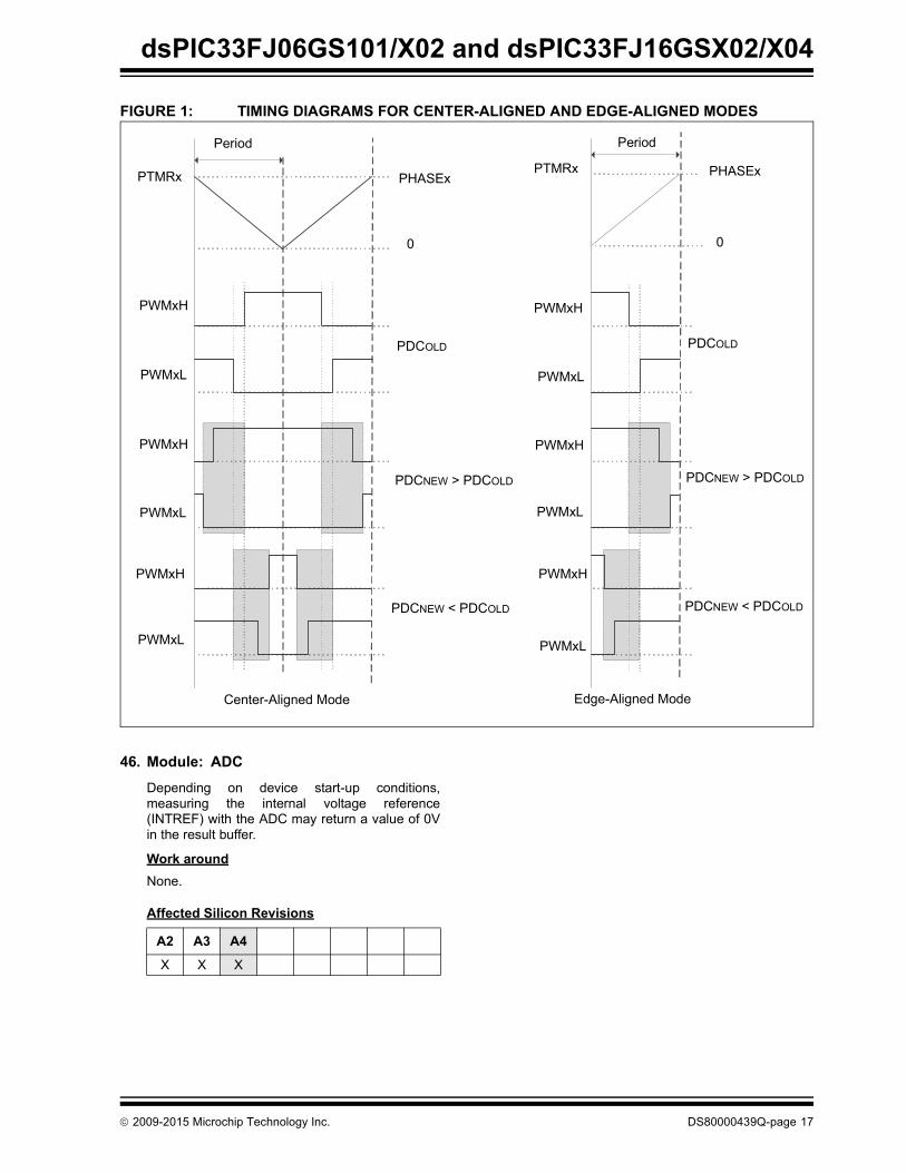
45. Module: PWM
The PWMx generator may not assert dead time onthe edges of transitions. This has been observedwhen all of the following conditions are present:
• The PWMx generator is configured to operate in Complementary mode with the independent time base or master time base;
• Immediate update is enabled; and • The value in the PDCx register is updated in
such a manner that the PWMxH and PWMxL outputs make an immediate transition.
The current duty cycle, PDCOLD, newly calculatedduty cycle, PDCNEW, and the point at which thewrite to the Duty Cycle register occurs within thePWMx time base, will determine if the PWMxH andPWMxL outputs make an immediate transition.PWMxH and PWMxL outputs make an immediatetransition if the Duty Cycle register is written with anew value, PDCNEW, at a point of time when thePWMx time base is counting a value that is inbetween PDCNEW and PDCOLD. Additionally,writing to the Duty Cycle register close to theinstant of time where dead time is being appliedmay result in reduced dead time, effective on thePWMxH and PWMxL transition edges.
In Figure 1 (following page), if the duty cycle writeoccurred in the shaded box, then PWMxH andPWMxL will make an immediate transition withoutdead time.
Work aroundNone. However, in most applications the dutycycle update timing can be controlled using theTRIGx trigger or Special Event Trigger such thatthe above mentioned conditions are avoidedaltogether.
Affected Silicon Revisions
A2 A3 A4
X X X
A2 A3 A4
X X X
A2 A3 A4
X X X
DS80000439Q-page 16 2009-2015 Microchip Technology Inc.
dsPIC33FJ06GS101/X02 and dsPIC33FJ16GSX02/X04
FIGURE 1: TIMING DIAGRAMS FOR CENTER-ALIGNED AND EDGE-ALIGNED MODES
46. Module: ADC
Depending on device start-up conditions,measuring the internal voltage reference(INTREF) with the ADC may return a value of 0Vin the result buffer.
Work aroundNone.
Affected Silicon Revisions
Center-Aligned Mode Edge-Aligned Mode
PWMxL
PWMxH
PWMxL
PWMxH
PWMxL
PWMxH
PTMRx
Period Period
PTMRx
0
PHASEx
PWMxH
PWMxH
PWMxH
PDCOLD
PDCNEW > PDCOLD
PDCNEW < PDCOLD
PWMxL
PDCNEW < PDCOLD
PDCNEW > PDCOLD
PDCOLD
0
PHASEx
PWMxL
PWMxL
A2 A3 A4
X X X
2009-2015 Microchip Technology Inc. DS80000439Q-page 17
dsPIC33FJ06GS101/X02 and dsPIC33FJ16GSX02/X04
47. Module: PWM
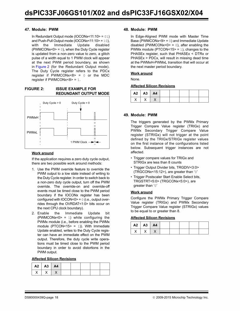
In Redundant Output mode (IOCONx<11:10> = 01)and Push-Pull Output mode (IOCONx<11:10> = 10),with the Immediate Update disabled(PWMCONx<0> = 0), when the Duty Cycle registeris updated from a non-zero value to zero, a glitchpulse of a width equal to 1 PWM clock will appearat the next PWM period boundary, as shownin Figure 2 (for the Redundant Output mode).The Duty Cycle register refers to the PDCxregister if PWMCONx<8> = 0 or the MDCregister if PWMCONx<8> = 1.
FIGURE 2: ISSUE EXAMPLE FOR REDUNDANT OUTPUT MODE
Work aroundIf the application requires a zero duty cycle output,there are two possible work around methods:
1. Use the PWM override feature to override thePWM output to a low state instead of writing tothe Duty Cycle register. In order to switch back toa non-zero duty cycle output, turn off the PWMoverride. The override-on and override-offevents must be timed close to the PWM periodboundary if the IOCONx register has beenconfigured with IOCON<0> = 0 (i.e., output over-rides through the OVRDAT<1:0> bits occur onthe next CPU clock boundary).
2. Enable the Immediate Update bit(PWMCONx<0> = 1) while configuring thePWMx module (i.e., before enabling the PWMxmodule (PTCON<15> = 1)). With ImmediateUpdate enabled, writes to the Duty Cycle regis-ter can have an immediate effect on the PWMoutput. Therefore, the duty cycle write opera-tions must be timed close to the PWM periodboundary in order to avoid distortions in thePWM output.
Affected Silicon Revisions
48. Module: PWM
In Edge-Aligned PWM mode with Master TimeBase (PWMCONx<9> = 0) and Immediate Updatedisabled (PWMCONx<0> = 0), after enabling thePWMx module (PTCON<15> = 1), changes to thePHASEx register, such that PHASEx < DTRx orPHASEx > PDCx, will result in missing dead timeat the PWMxH-PWMxL transition that will occur atthe next master period boundary.
Work aroundNone.
Affected Silicon Revisions
49. Module: PWM
The triggers generated by the PWMx PrimaryTrigger Compare Value register (TRIGx) andPWMx Secondary Trigger Compare Valueregister (STRIGx) will not trigger at the pointdefined by the TRIGx/STRIGx register valueson the first instance of the configurations listedbelow. Subsequent trigger instances are notaffected.
• Trigger compare values for TRIGx and STRIGx are less than 8 counts
• Trigger Output Divider bits, TRGDIV<3:0> (TRGCONx<15:12>), are greater than ‘0’
• Trigger Postscaler Start Enable Select bits, TRGSTRT<5:0> (TRGCONx<5:0>), are greater than ‘0’
Work aroundConfigure the PWMx Primary Trigger CompareValue register (TRIGx) and PWMx SecondaryTrigger Compare Value register (STRIGx) valuesto be equal to or greater than 8.
Affected Silicon Revisions
A2 A3 A4
X X X
1 PWM Clock
Duty Cycle > 0 Duty Cycle = 0
PWMxH
PWMxL
A2 A3 A4
X X X
A2 A3 A4
X X X
DS80000439Q-page 18 2009-2015 Microchip Technology Inc.

dsPIC33FJ06GS101/X02 and dsPIC33FJ16GSX02/X04
50. Module: I2C
In Slave mode, clock stretching may not occur,even when it has been enabled (STREN = 1). Asa result, the SCLREL bit may not be cleared uponaddress reception when the R/W bit is ‘0’. This isseen in both 7-Bit and 10-Bit Address modes.
Work aroundNone.
Affected Silicon Revisions
Data Sheet ClarificationsThe following typographic corrections and clarificationsare to be noted for the latest version of the device datasheet (DS70000318G):
None.
A2 A3 A4
X X X
Note: Corrections are shown in bold. Wherepossible, the original bold text formattinghas been removed for clarity.
2009-2015 Microchip Technology Inc. DS80000439Q-page 19
dsPIC33FJ06GS101/X02 and dsPIC33FJ16GSX02/X04
APPENDIX A: REVISION HISTORYRev A Document (3/2009)
Initial release of this document; issued for revision A2silicon.
Includes silicon issues 1-9 (PWM), 10 (Comparator), 11(ADC), 12 (Auxiliary Clock), 13 (Comparator), 14-15(UART) and 16 (I2C™).
Rev B Document (4/2009)
Added silicon issue 17 (PWM).
Rev C Document (5/2009)
Updated silicon issue 17 (PWM) to clarify which ADCpairs are involved.
Rev D Document (5/2009)
Revised to include revision A3 silicon information.Added silicon issues 18 (Core), 19 (UART) and 20-21(PWM).
Added data sheet clarification 1 (The followingtypographic corrections and clarifications are to be notedfor the latest version of the device data sheet(DS70000318G):).
Rev E Document (8/2009)
Added silicon issues 22-23 (UART), 24-25 (I2C), 26(PSV Operations), 27 (Comparator) and 28 (PWM).
Rev F Document (1/2010)
Added silicon issues 29 (Analog Comparator) and30 (Auxiliary PLL).
Added data sheet clarification 2 (Auxiliary PLL).
Rev G Document (6/2010)
Added silicon issues 31 (ADC) and 32 (High-SpeedPWM) and data sheet clarification 3 (DC Characteristics:I/O Pin Input Specifications).
Rev H Document (10/2010)
Added revision A4 silicon information to all tables.
Updated the work arounds for silicon issue 31 (ADC).
Removed silicon issue 33 (PWM) and marked itslocation as reserved.
Added silicon issues 34 (PWM) and 35 (JTAG).
Rev J Document (3/2011)
Updated silicon issue 29 (Analog Comparator).
Added silicon issues 36 (SPI) and 37 (Comparator).
Added data sheet clarification 4.
Rev K Document (11/2011)
Added silicon issues 38 (CPU), 39 (CPU), 40 (UART),41 (JTAG), and 42 (PWM).
Rev L Document (5/2012)
Removed data sheet clarifications 2, 3 and 4.
Updated silicon issues 29 (Analog Comparator) and32 (High-Speed PWM).
Added silicon issues 43 (PWM) and 44 (PWM).
Rev M Document (1/2013)
Amended silicon issue 43 with correct PWM ClockDivider Select register bit name (changed from PTCONto PTCON2).
Included silicon issue 45 (PWM).
Rev N Document (9/2013)
Removed existing silicon issue 42 (PWM); subsequentissues are renumbered accordingly.
Added new silicon issues 45 (PWM) and 46 (ADC).
Added new data sheet clarification 2 (Packaging).
Corrected the module for issue 18 from “PGEC3/PGED3Programming Pins” to “Core”, to conform with standardnomenclature practice (the issue itself is unchanged).
Rev P Document (10/2014)
Added new silicon issues 47, 48 and 49 (PWM).
Removed data sheet clarifications 1 and 2.
Rev Q Document (1/2015)
Added new silicon issue 50 (I2C).
DS80000439Q-page 20 2009-2015 Microchip Technology Inc.

Note the following details of the code protection feature on Microchip devices:• Microchip products meet the specification contained in their particular Microchip Data Sheet.
• Microchip believes that its family of products is one of the most secure families of its kind on the market today, when used in the intended manner and under normal conditions.
• There are dishonest and possibly illegal methods used to breach the code protection feature. All of these methods, to our knowledge, require using the Microchip products in a manner outside the operating specifications contained in Microchip’s Data Sheets. Most likely, the person doing so is engaged in theft of intellectual property.
• Microchip is willing to work with the customer who is concerned about the integrity of their code.
• Neither Microchip nor any other semiconductor manufacturer can guarantee the security of their code. Code protection does not mean that we are guaranteeing the product as “unbreakable.”
Code protection is constantly evolving. We at Microchip are committed to continuously improving the code protection features of ourproducts. Attempts to break Microchip’s code protection feature may be a violation of the Digital Millennium Copyright Act. If such actsallow unauthorized access to your software or other copyrighted work, you may have a right to sue for relief under that Act.
Information contained in this publication regarding deviceapplications and the like is provided only for your convenienceand may be superseded by updates. It is your responsibility toensure that your application meets with your specifications.MICROCHIP MAKES NO REPRESENTATIONS ORWARRANTIES OF ANY KIND WHETHER EXPRESS ORIMPLIED, WRITTEN OR ORAL, STATUTORY OROTHERWISE, RELATED TO THE INFORMATION,INCLUDING BUT NOT LIMITED TO ITS CONDITION,QUALITY, PERFORMANCE, MERCHANTABILITY ORFITNESS FOR PURPOSE. Microchip disclaims all liabilityarising from this information and its use. Use of Microchipdevices in life support and/or safety applications is entirely atthe buyer’s risk, and the buyer agrees to defend, indemnify andhold harmless Microchip from any and all damages, claims,suits, or expenses resulting from such use. No licenses areconveyed, implicitly or otherwise, under any Microchipintellectual property rights.
2009-2015 Microchip Technology Inc.
QUALITY MANAGEMENT SYSTEM CERTIFIED BY DNV
== ISO/TS 16949 ==
Trademarks
The Microchip name and logo, the Microchip logo, dsPIC, FlashFlex, flexPWR, JukeBlox, KEELOQ, KEELOQ logo, Kleer, LANCheck, MediaLB, MOST, MOST logo, MPLAB, OptoLyzer, PIC, PICSTART, PIC32 logo, RightTouch, SpyNIC, SST, SST Logo, SuperFlash and UNI/O are registered trademarks of Microchip Technology Incorporated in the U.S.A. and other countries.
The Embedded Control Solutions Company and mTouch are registered trademarks of Microchip Technology Incorporated in the U.S.A.
Analog-for-the-Digital Age, BodyCom, chipKIT, chipKIT logo, CodeGuard, dsPICDEM, dsPICDEM.net, ECAN, In-Circuit Serial Programming, ICSP, Inter-Chip Connectivity, KleerNet, KleerNet logo, MiWi, MPASM, MPF, MPLAB Certified logo, MPLIB, MPLINK, MultiTRAK, NetDetach, Omniscient Code Generation, PICDEM, PICDEM.net, PICkit, PICtail, RightTouch logo, REAL ICE, SQI, Serial Quad I/O, Total Endurance, TSHARC, USBCheck, VariSense, ViewSpan, WiperLock, Wireless DNA, and ZENA are trademarks of Microchip Technology Incorporated in the U.S.A. and other countries.
SQTP is a service mark of Microchip Technology Incorporated in the U.S.A.
Silicon Storage Technology is a registered trademark of Microchip Technology Inc. in other countries.
GestIC is a registered trademarks of Microchip Technology Germany II GmbH & Co. KG, a subsidiary of Microchip Technology Inc., in other countries.
All other trademarks mentioned herein are property of their respective companies.
© 2009-2015, Microchip Technology Incorporated, Printed in the U.S.A., All Rights Reserved.
ISBN: 978-1-63276-992-3
Microchip received ISO/TS-16949:2009 certification for its worldwide
DS80000439Q-page 21
headquarters, design and wafer fabrication facilities in Chandler and Tempe, Arizona; Gresham, Oregon and design centers in California and India. The Company’s quality system processes and procedures are for its PIC® MCUs and dsPIC® DSCs, KEELOQ® code hopping devices, Serial EEPROMs, microperipherals, nonvolatile memory and analog products. In addition, Microchip’s quality system for the design and manufacture of development systems is ISO 9001:2000 certified.

DS80000439Q-page 22 2009-2015 Microchip Technology Inc.
AMERICASCorporate Office2355 West Chandler Blvd.Chandler, AZ 85224-6199Tel: 480-792-7200 Fax: 480-792-7277Technical Support: http://www.microchip.com/supportWeb Address: www.microchip.comAtlantaDuluth, GA Tel: 678-957-9614 Fax: 678-957-1455Austin, TXTel: 512-257-3370 BostonWestborough, MA Tel: 774-760-0087 Fax: 774-760-0088ChicagoItasca, IL Tel: 630-285-0071 Fax: 630-285-0075ClevelandIndependence, OH Tel: 216-447-0464 Fax: 216-447-0643DallasAddison, TX Tel: 972-818-7423 Fax: 972-818-2924DetroitNovi, MI Tel: 248-848-4000Houston, TX Tel: 281-894-5983IndianapolisNoblesville, IN Tel: 317-773-8323Fax: 317-773-5453Los AngelesMission Viejo, CA Tel: 949-462-9523 Fax: 949-462-9608New York, NY Tel: 631-435-6000San Jose, CA Tel: 408-735-9110Canada - TorontoTel: 905-673-0699 Fax: 905-673-6509
ASIA/PACIFICAsia Pacific OfficeSuites 3707-14, 37th FloorTower 6, The GatewayHarbour City, KowloonHong KongTel: 852-2943-5100Fax: 852-2401-3431Australia - SydneyTel: 61-2-9868-6733Fax: 61-2-9868-6755China - BeijingTel: 86-10-8569-7000 Fax: 86-10-8528-2104China - ChengduTel: 86-28-8665-5511Fax: 86-28-8665-7889China - ChongqingTel: 86-23-8980-9588Fax: 86-23-8980-9500China - HangzhouTel: 86-571-8792-8115 Fax: 86-571-8792-8116China - Hong Kong SARTel: 852-2943-5100 Fax: 852-2401-3431China - NanjingTel: 86-25-8473-2460Fax: 86-25-8473-2470China - QingdaoTel: 86-532-8502-7355Fax: 86-532-8502-7205China - ShanghaiTel: 86-21-5407-5533 Fax: 86-21-5407-5066China - ShenyangTel: 86-24-2334-2829Fax: 86-24-2334-2393China - ShenzhenTel: 86-755-8864-2200 Fax: 86-755-8203-1760China - WuhanTel: 86-27-5980-5300Fax: 86-27-5980-5118China - XianTel: 86-29-8833-7252Fax: 86-29-8833-7256China - XiamenTel: 86-592-2388138 Fax: 86-592-2388130China - ZhuhaiTel: 86-756-3210040 Fax: 86-756-3210049
ASIA/PACIFICIndia - BangaloreTel: 91-80-3090-4444 Fax: 91-80-3090-4123India - New DelhiTel: 91-11-4160-8631Fax: 91-11-4160-8632India - PuneTel: 91-20-3019-1500Japan - OsakaTel: 81-6-6152-7160 Fax: 81-6-6152-9310Japan - TokyoTel: 81-3-6880- 3770 Fax: 81-3-6880-3771Korea - DaeguTel: 82-53-744-4301Fax: 82-53-744-4302Korea - SeoulTel: 82-2-554-7200Fax: 82-2-558-5932 or 82-2-558-5934Malaysia - Kuala LumpurTel: 60-3-6201-9857Fax: 60-3-6201-9859Malaysia - PenangTel: 60-4-227-8870Fax: 60-4-227-4068Philippines - ManilaTel: 63-2-634-9065Fax: 63-2-634-9069SingaporeTel: 65-6334-8870Fax: 65-6334-8850Taiwan - Hsin ChuTel: 886-3-5778-366Fax: 886-3-5770-955Taiwan - KaohsiungTel: 886-7-213-7830Taiwan - TaipeiTel: 886-2-2508-8600 Fax: 886-2-2508-0102Thailand - BangkokTel: 66-2-694-1351Fax: 66-2-694-1350
EUROPEAustria - WelsTel: 43-7242-2244-39Fax: 43-7242-2244-393Denmark - CopenhagenTel: 45-4450-2828 Fax: 45-4485-2829France - ParisTel: 33-1-69-53-63-20 Fax: 33-1-69-30-90-79Germany - DusseldorfTel: 49-2129-3766400Germany - MunichTel: 49-89-627-144-0 Fax: 49-89-627-144-44Germany - PforzheimTel: 49-7231-424750Italy - Milan Tel: 39-0331-742611 Fax: 39-0331-466781Italy - VeniceTel: 39-049-7625286 Netherlands - DrunenTel: 31-416-690399 Fax: 31-416-690340Poland - WarsawTel: 48-22-3325737 Spain - MadridTel: 34-91-708-08-90Fax: 34-91-708-08-91Sweden - StockholmTel: 46-8-5090-4654UK - WokinghamTel: 44-118-921-5800Fax: 44-118-921-5820
Worldwide Sales and Service
03/25/14