dspic33c dsc design guidelines - microchip.com
TRANSCRIPT

A Leading Provider of Smart, Connected and Secure Embedded Control Solutions
dsPIC33C Digital Signal ControllerDesign Guidelines
dsPIC33C Digital Signal Controllers

Generic Robust Guideline
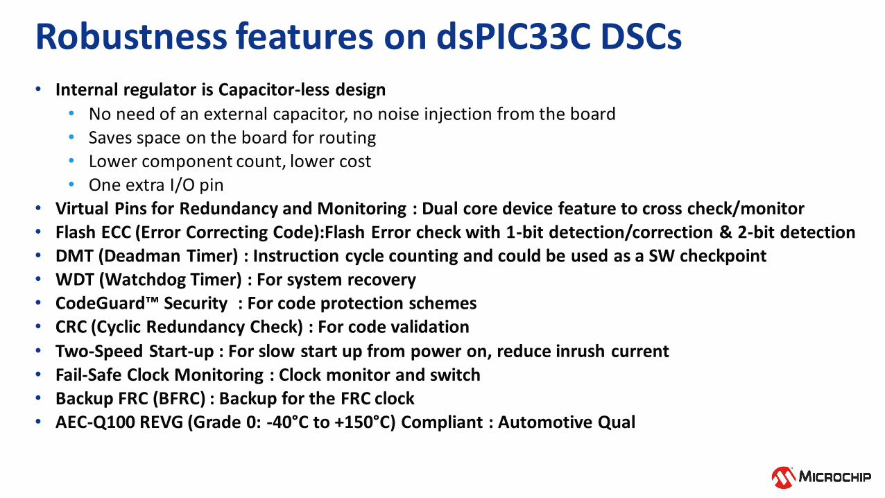
Robustness features on dsPIC33C DSCs• Internal regulator is Capacitor-less design
• No need of an external capacitor, no noise injection from the board• Saves space on the board for routing• Lower component count, lower cost• One extra I/O pin
• Virtual Pins for Redundancy and Monitoring : Dual core device feature to cross check/monitor • Flash ECC (Error Correcting Code):Flash Error check with 1-bit detection/correction & 2-bit detection• DMT (Deadman Timer) : Instruction cycle counting and could be used as a SW checkpoint• WDT (Watchdog Timer) : For system recovery • CodeGuard™ Security : For code protection schemes• CRC (Cyclic Redundancy Check) : For code validation
• Two-Speed Start-up : For slow start up from power on, reduce inrush current• Fail-Safe Clock Monitoring : Clock monitor and switch• Backup FRC (BFRC) : Backup for the FRC clock• AEC-Q100 REVG (Grade 0: -40°C to +150°C) Compliant : Automotive Qual

Decoupling Capacitor
• For wide frequency noise filtering, provide multiple decoupling capacitors (e.g.0.01uF,0.1uF) across supply pins of dsPIC33C DSC
• When multiple capacitors are provided, place them in ascending order of their value with lowest value capacitor closest to the dsPIC33C pin
• Provide decoupling capacitors between each VDD/GND pair of the dsPIC33C DSC
• Place decoupling capacitors close to VDD and GND pin pairs of the dsPIC33C DSC
• Connect dsPIC33C DSC pin and capacitor pads using shorter direct traces without any vias between them
• Also connect decoupling capacitor between AVDD and AGND using shorter traces
Decoupling Caps :AVDD -AGND
Decoupling Caps : DVDD - DGND

Oscillator and MCLR
• Place crystal oscillator close to OSCI/OSCO pins of the dsPIC33C DSC and connect it using short direct traces avoiding vias
• Provide isolated ground plane under the crystal, connect this ground Isle to Board Ground
• Avoid any high-speed signals running near the oscillator circuit
• Add series resistor between reset pushbutton and MCLR pin of the dsPIC33C DSCs
5

Current feedbacksFrom shunt to amplifier inputs
• Use Kelvin sensing – take separate traces from pads of the shunt resistor for connecting to amplifier input resistors
• Take the current feedbacks traces from shunt resistor as differential pair running parallel across the board until it is connected to amplifier input resistors (which are placed closer to amplifier positive and negative input pins)
6

Ground ConnectionAnalog and Digital Ground
• Separate the ground of digital circuits, analog circuits ,high speed circuit, high current circuit etc.
• The separated ground must be connected only at supply start point which is closer to the 3.3V LDO (dsPIC33C DSC Supply)
• In case of multilayer board, dedicate at least one internal layer for grounds. Try to provide solid ground plane avoiding any cuts
• To do this , it is necessary to identify the components that connect to specific ground and place them close to each other in specific area of the board
7
Example :Solid internal Analog Ground(AGND) plane joining at LDO ground.
Digital Ground (DGND) trace Analog Ground (AGND) trace
AGND and DGND are joined at one point near the source using net tie.

Low Noise Guideline

Weak Spot ADCAnalog-To-Digital Converter Circuit• Increasing CPU speed with shrinking structure sizes result in an increased sensitivity to noise
• CPU load transient frequencies stimulate passive/reactive circuits formed by parasitic RLC resonators (PCB)
• Digital high-speed peripherals add to noise level
• In control applications, the ADC is the most sensitive element and provides the guiding value for noise budget estimations
• Power Electronics Control Applications are most sensitive to ADC accuracy• Limited Resolution limits dynamic range of control loop
• Noise on feedback signal reproduces on ADC results
• Noise on supply lines influences internal references
• Faster ADCs generate more noise within the internal, analog circuit
DIGITIZEDBLOCK ADC
Power
Stage
(Plant)
Error
Amplifier+ –
PWM
(Modulator)
Voltage
Divider
REFV
ERROR REF OUTV V K V= −
EAV D
K
OUTV
INV

Noise BudgetHow much noise is acceptable?• Determine maximum acceptable voltage deviation
• The most system element influencing the most sensitive parameter of the product determines the acceptance level
• In power conversion, this is output voltage / output current accuracy and response characteristic
• Both highly depend on reliable ADC results
10
Power Converter
Circuit
VINVOUT
ADC
REF
VFB
error+
-𝐻𝐶 𝑧
(Compensator)output
input
Anti-
Windup
PWM
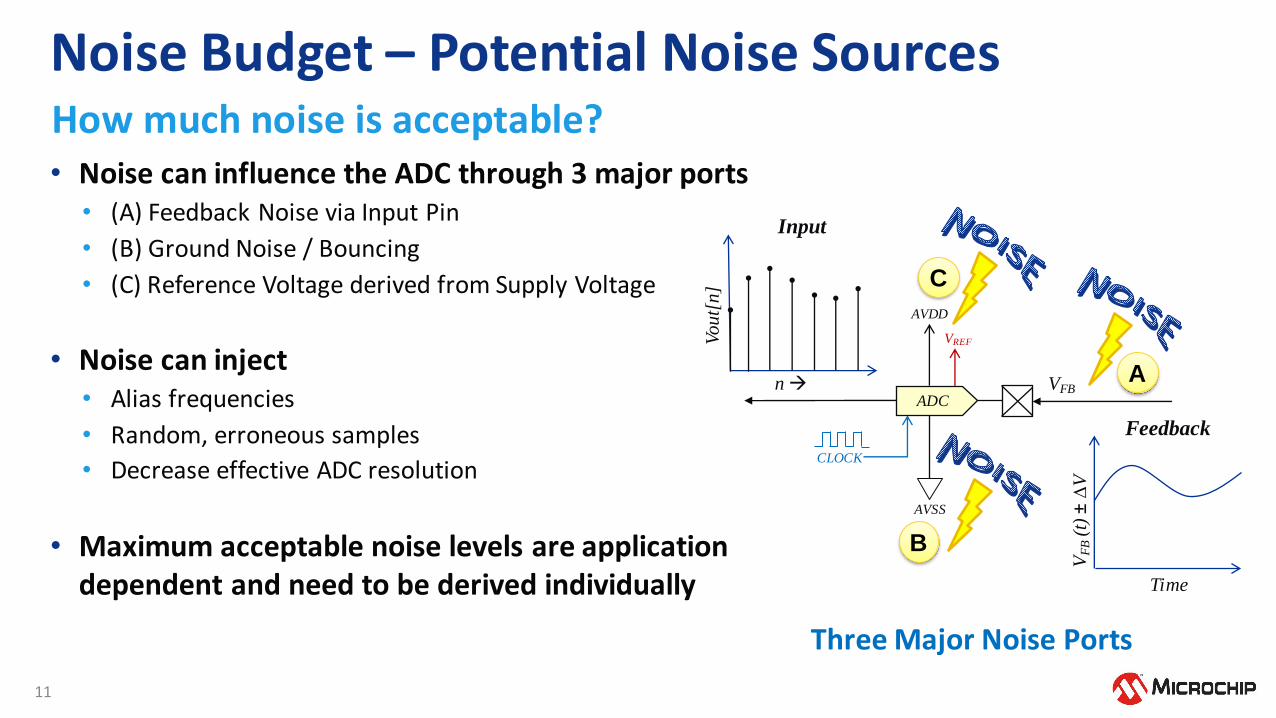
Noise Budget – Potential Noise SourcesHow much noise is acceptable?• Noise can influence the ADC through 3 major ports
• (A) Feedback Noise via Input Pin
• (B) Ground Noise / Bouncing
• (C) Reference Voltage derived from Supply Voltage
• Noise can inject• Alias frequencies
• Random, erroneous samples
• Decrease effective ADC resolution
• Maximum acceptable noise levels are application dependent and need to be derived individually
11
VFB
VF
B(t
) ±
V
Time
Feedback
Vo
ut[
n]
n →
Input
CLOCK
AVSS
AVDD
VREF
A
B
C
Three Major Noise Ports
ADC

Noise Port (A): Alias-Free DesignAlias Frequencies• Random noise on feedback signals are relatively uncritical
• Periodic noise components exceeding the minimum ADC granularity may influence ADC results
• If these are at around or higher than fSAM/2, alias-frequencies may be injected
• High-speed ADCs with very small Sample & Hold (S&H)• Capacitance and short sampling times are getting increasingly sensitive to periodic noise on feedback signals
• Once alias frequencies have been injected in the data stream, they may influence the control system.
• Recommended to add anti-alias filters to input pins, tuned for the effective sampling frequency of the application while still allowing relevant transients to pass.
12
-1.5
-1
-0.5
0
0.5
1
1.5
0 45 90 135 180 225 270 315 360
Waveform Sampled at fN
Feedback Sampled Input
Frequency
Ma
gn
itu
de
10050
𝒇𝑺𝑨𝑴𝟐 𝒇𝑺𝑨𝑴𝟕
𝟎𝒌𝑯𝒛
𝟒𝟎𝒌𝑯𝒛
𝟑𝟎𝒌𝑯𝒛
𝟐𝟓𝒌𝑯𝒛
𝟏𝟎𝒌𝑯𝒛 𝟏𝟔𝟎𝒌𝑯𝒛
𝟓𝟏𝟎𝒌𝑯𝒛
Inp
ut
Fre
qu
en
cy
Inp
ut
Fre
qu
en
cy
Inp
ut
Fre
qu
en
cy

Noise Port (A): Alias-Free DesignAnti-Alias Filter DesignAdjustment of anti-alias cut-off frequencies need to consider the internal ADC architecture to prevent excessive ADC result deviations
• Shared ADC CoresADC cores with multiple analog input pins (ANx) connect the single S&H capacitor to the pin via multiplexers. To prevent cross-talk between input channels, the S&H capacitor needs to be discharged before connection. When connected, the S&H capacitor needs enough time to charge up to the feedback voltage level to achieve an accurate result.
• Dedicated ADC CoresDedicated cores continuously keep their S&H connected to the pin, tracking the feedback voltage. The connection is only opened during conversion and closed when conversion has completed
13
ADCVFB*
VFB
C

Noise Port (A): Alias-Free DesignAnti-Alias Filter Design / Shared ADC Core• Step 1: Decoupling Capacity
• During sampling using the shared ADC core, the discharged S&H capacitor CHOLD is connected to the feedback circuit. CHOLD is charged through RSS and RIC (~350 W). The high charging current right after SWSS is closed injects a fast transient into the feedback line. Depending on the distance between the voltage divider and the device input pin, the parasitic trace inductance might prevent to bias this inrush current. Hence, this current is exclusively biased by decoupling capacitor C, eventually forming a capacitive voltage divider with CHOLD. As a result, the final sampling voltage will always settle below the real feedback voltage VFB introducing a measurement error of
Error = 1 −𝐶𝐻𝑂𝐿𝐷
𝐶(first assessment of the static offset)
• Software adjustable sampling times allow accounting for and thus minimizing these effects which, however, increases the data acquisition latency. For high-speed designs it is therefore recommended to minimize the static error by placing enough capacitance as close as possible at the ADC input pin (recommended value = 30…50 x CHOLD).
14
VFB*VFB
C
R
VOUT
CPINCHOLD
VDD
RICRSS
Sampling Switch
ILEAKAGES
LTRACE
Parasitic Trace
Inductance
CDRB
SWSS

Noise Port (A): Alias-Free DesignAnti-Alias Filter Design / Shared ADC Core• Step 2: Filter Resistor
• Peak-to-Peak voltage levels of periodic noise should be limited to the voltage equivalent of approx. 3 LSB. At VREF = 3.3V and 12-bit resolution the ADC has a total granularity of 806 µV/tick. 3 LSB therefore have a voltage equivalent of 6.44 mV. The total acceptable level,however, depends on the total feedback signal range and needs to be calculated for every application individually.
Example:
• A signal is sampled at fSAM = 500 kHz (Nyquist-Shannon limit at fN = 250 kHz). A dominant, periodic noise component fNoise = 1000 kHz with a max. deviation of VNoise pk-pk = 60mV is observed. To prevent alias frequencies being injected into the ADC data stream, this noise needs to be damped to less than 6.44 V @ fN. (-20dB @ fN = 6 mV). The pole introduced by the RC filter therefore needs to be placed one magnitude below fN (=25 kHz) to effectively damp the noise magnitude at fN by factor 10.
15
VFB*VFB
C
R
VOUT
CPINCHOLD
VDD
Distance X
RICRSS
Sampling Switch
ILEAKAGES
LTRACE
Parasitic Trace
Inductance
CD
RA
RB
SWSS

Noise Port (A): Alias-Free DesignAnti-Alias Filter Design / Shared ADC Core• Step 3: Recharging Decoupling Capacitor C
• After the sampling transient has passed, decoupling capacitor C needs to be recharged up to the feedback level for the next sample. With high resistive voltage divider networks, it is recommended to place an additional decoupling capacitor in parallel to the lower voltage divider resistor. This capacitor also helps to compensate the parasitic trace inductance LTRACE. At high sampling frequencies hand high resistive voltage dividers an operational amplifier might be required to recharge C in time for the next sample.
16
VFB*VFB
C
R
VOUT
CPINCHOLD
VDD
Distance X
RICRSS
Sampling Switch
ILEAKAGES
LTRACE
Parasitic Trace
Inductance
CD
RA
RB
SWSS

Noise Port (A): Alias-Free DesignAnti-Alias Filter Design / Shared ADC Core• Design Tip:
• Power electronics designs are commonly noisy as the circuit itself produces noise over a very wide frequency range up to manyGHz. Dominant noise bands in the range of 8-15 MHz caused by Diode ringing as well as harmonics of the switching frequency are sometimes difficult to contain and might be induced in feedback lines. The magnitude of the induced noise is independent from the voltage level present.
• Hence, it is recommended to place the voltage divider close to the device, minimizing Distance X as well as the parasitic trace inductance LTRACE. Especially, however, preventing noise from being induced in low voltage signals. Noise induced on high voltage signals will get divided with the feedback signal and will therefore have lower amplitudes requiring less damping and thus expanding the maximum bandwidth of the feedback signal.
17
VFB*VFB
C
R
VOUT
CPINCHOLD
VDD
Distance X
RICRSS
Sampling Switch
ILEAKAGES
LTRACE
Parasitic Trace
Inductance
CD
RA
RB
SWSS

Noise Budget – Potential Noise SourcesHow much noise is acceptable?• In addition to adjust noise filtering on feedback signals, it is required to analyze the noise floor on
supply and ground lines• The ADC uses a reference voltage, which is derived from the supply voltage
• Noise on this supply rail can influence the reference level during a conversion process, equally perturbing ADC results as sampling noisy signals.
• Supply rain noise can enter the system through VDD as well as through VSS
18
VFB
VF
B(t
) ±
V
Time
Feedback
Vout[
n]
n →
Input
CLOCK
AVSS
AVDD
VREF
A
B
C
ADC

Noise Budget – Flat Impedance DesignSymmetrical Layout
• The CPU itself is a potential noise hub in the system. Each instruction executed by the CPU will create a load step with low amplitude but high edge speed. These high frequency current pulses are exclusively biased by the decoupling capacitors. The generated AC noise inevitably migrates into supply and ground traces, forward into the device as well as backwards to the voltage regulator (VRM).
• Insufficient decoupling can stimulate passive/reactive elements along the way, which, if stimulated in the right frequency, may start to resonate, increasing the noise level.
19
FB
VDD/VSS
ANALOG INPUTS
C
D
LOAD
Voltage Regulator Module(VRM)
Passive/Reactive NetworkActive Network
VREF
C DA B
dsPIC33C DSC
C
C
C
Digital Ground
Analog Ground
LDO
AB
ESR
C
ESL
LO
AD
IL
IESL
VDD
VSS
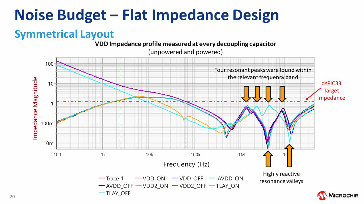
Noise Budget – Flat Impedance DesignSymmetrical Layout
20
Four resonant peaks were found within the relevant frequency band
VDD Impedance profile measured at every decoupling capacitor(unpowered and powered)
dsPIC33 Target
Impedance
Highly reactive resonance valleys
Imp
edan
ce M
agn
itu
de

Noise Budget – Flat Impedance DesignSymmetrical Layout
21
dsPIC33 Target
Impedance
window of interest
Stimulus window
Total VDD Impedance profile measured at PDN Port BCPU Clock Frequencies
fCY
2
fCY fOSC

Noise Budget - Flat Impedance DesignKey Takeaways• Key Takeaways
• Sharp valleys in an impedance profile indicate the presence of resonance/anti-resonance frequencies of passive/reactive network elements
• The CPU load profile is determined by instruction execution and peripheral activity, which are both software dependent to a high degree
• The faster the CPU, the wider the frequency range across potential stimuli can be injected into the passive/reactive network segment
• If one or more resonators are stimulated simultaneously, the noise level may inflationary increase (Rouge Wave)
• Remedy: Flat Impedance Design• Output impedance of voltage regulator must match target impedance• Decoupling capacitors must be selected to match/cancel excess inductance (traces)• Symmetrical design (equal trace length and width of VDD lines reduce number of resonant peaks)• Using ground planes instead of traces reduce VSS trace impedance, shifting potential resonant peaks
into high frequency range beyond the Window Of Interest
Please note: Although passive/reactive network components may still be stimulated by higher frequencies within the Stimulus Window, the CPU won’t be able to pick them up.
22

Noise Budget – Target ImpedanceFlat Impedance Design
• Determining Target Impedance ZTARGET
• Determine max. acceptable voltage deviation for the application• ADC being the most sensitive element (ADC sample tolerance, e.g. 10mV)
• Determine minimum and maximum load current, depending on CPU speed and peripheral usage (e.g. Imin = 40mA, Imax = 80mA)
Example:
23
minmax
argII
ToleranceVZ DD
etT−
=
𝑍𝑇 arg 𝑒𝑡 =3.3𝑉 × 0.010 𝑉
0.080𝐴 − 0.040 𝐴= 0.825W

Symmetrical Layout and DecouplingExcess Impedance Cancellation
• Positive supply traces (VDD) between PDN port (B) and decoupling ports (C) should be as symmetrical as possible to prevent potential resonant frequencies spreading into multiple peaks concentrated in a narrow frequency range.
• Decoupling capacitance need to be selected to cancel the excess inductance of the supply traces. Too much or less capacitance will inevitably result in resonant tank becoming reactive to stimuli. A symmetrical design will allow to use the same capacitance at every decoupling point (C)
• Analog supply voltage is best taken from the nearest decoupling point (C) being filtered through a ferrite bead (E)
FB
VDD/VSS
ANALOG INPUTS
C
D
C
C
C
LDO
AB
E

Symmetrical Layout and DecouplingExcess Impedance Cancellation
• Using ground planes instead of traces lowers the excess inductance, effectively moving potential resonant frequencies to higher ranges and eventually out of the Window Of Interest
• Digital and analog ground should always be separated preventing noise produced by the CPU entering sensitive analog circuits
• Prevent ground planes from overlapping and accidentally coupling noise between planes
• Ground decoupling can be done by• Plane gaps, introducing a slightly increased resistance and
inductance between both planes limiting noise from migrating
• Putting 0 W resistors in between planes introducing the package inductance as a filter barrier
• Replacing 0 W resistors by ferrite beads for a more specific filter characteristicFB
VDD/VSS
ANALOG INPUTS
C
D
C
C
C
Digital Ground
Analog Ground
E
ShieldVSS AVSS
0R0R

Analog Rail DecouplingVDD-2-AVDD Filtering
• Digital noise generated by the CPU on VDD gets contained within the network segment by putting up a barrier between VDD and AVDD:
• Ferrite Beads allow selective filtering of frequency bands while ensuring proper balancing of decoupling capacitors on VDD and AVDD (recommended)
• Low Resistance Resistors also introduce some small package inductance as well provide resistance adding to lowering the Q resp. increase damping (e.g. 4.7 W)
• Gapping of layout traces will have similar effects like the options above, but their effectiveness is questionable (not recommended in general)
FB
VDD/VSS
ANALOG INPUTS
C
D
C
C
C
Digital Ground
Analog Ground
E
VSS AVSS
FBVDD AVDD
0R

Additional Design GuidanceDesign Example & Documents
dsPIC33C DSC Design Reference:
dsPIC33CH512MP506 Digital Power Plug-In Module (DP-PIM), Part-No. MA330049
Anti-Alias Filter Design Guidance:
dsPIC33CH512MP506 DP-PIM User Guide / Appendix C. Characterization Data
27