dsp56367 data sheet -...
TRANSCRIPT

© Freescale Semiconductor, Inc., 2001, 2002, 2003, 2004, 2005, 2006, 2007. All rights reserved.
Freescale SemiconductorData Sheet: Technical Data
This document contains information on a new product. Specifications and information herein are subject to change without notice.
Document Number: DSP56367Rev. 2.1, 1/2007
1 OverviewThis document briefly describes the DSP56367 24-bit digital signal processor (DSP). The DSP56367 is a member of the DSP56300 family of programmable CMOS DSPs. The DSP56367 is targeted to applications that require digital audio compression/decompression, sound field processing, acoustic equalization and other digital audio algorithms. The DSP56367 offers 150 million instructions per second (MIPS) using an internal 150 MHz clock at 1.8 V and 100 million instructions per second (MIPS) using an internal 100 MHz clock at 1.5 V.
DSP5636724-Bit Audio Digital Signal Processor
Contents1 Overview . . . . . . . . . . . . . . . . . . . . . . . . . . . . 1-12 Signal/Connection Descriptions . . . . . . . . . . . 2-13 Specifications . . . . . . . . . . . . . . . . . . . . . . . . . 3-14 Packaging. . . . . . . . . . . . . . . . . . . . . . . . . . . . 4-15 Design Considerations . . . . . . . . . . . . . . . . . . 5-1A Power Consumption Benchmark . . . . . . . . . . A-1

Overview
DSP56367 Technical Data, Rev. 2.1
1-2 Freescale Semiconductor
Figure 1-1 DSP56367 Block Diagram
Data Sheet ConventionsThis data sheet uses the following conventions:
OVERBAR Used to indicate a signal that is active when pulled low (For example, the RESET pin is active when low.)
“asserted” Means that a high true (active high) signal is high or that a low true (active low) signal is low
“deasserted” Means that a high true (active high) signal is low or that a low true (active low) signal is high
Examples: Signal/Symbol Logic State Signal State Voltage*
PIN True Asserted VIL / VOL
PIN False Deasserted VIH / VOH
PIN True Asserted VIH / VOH
PIN False Deasserted VIL / VOL
Note:*Values for VIL, VOL, VIH, and VOH are defined by individual product specifications.
CLOCKGENERATOR
INTERNAL DATABUS
SWITCH
EXTAL
PROGRAM RAM
/INSTR. CACHE3K x 24
PROGRAM ROM
40K x 24Bootstrap ROM
192 x 24
PROGRAMINTERRUPT
CONTROLLER
PROGRAMDECODE
CONTROLLE
PROGRAMADDRESS
GENERATOR
YABXABPAB
YDBXDBPDBGDB
MODA/IRQAMODB/IRQB
DATA ALU24X24+56->56-BIT MAC
TWO 56-BIT ACCUMULATORSBARREL SHIFTER
MODC/IRQC
PLL
OnCE™
HOSTINTER-FACE
DAX(SPDIF Tx.)INTERFACE
416
X MEMORY
RAM13K X 24
ROM32K x 24
Y MEMORY
RAM7K X 24
ROM8K x 24
DDB
DABSIX CHANNELSDMA UNIT
MEMORY EXPANSION AREA
PERIPHERAL
YM
_EB
XM
_EB
PM
_EB
PIO
_EB
24 BITS BUS
EXPANSION AREA
JTAG 4
5
RESET
POWERMNGMNT
PINIT/NMI
2
TRIPLETIMER
1
MODD/IRQD
DRAM & SRAM BUS INTERFACE
& I - CACHE
EXTERNALADDRESS
BUSSWITCH
EXTERNALDATA BUSSWITCH
ADDRESS
10
DATA
CONTROL
24
18
ESAI INTER-FACE
86
ESAI_1
ADDRESSGENERATION
UNIT
24-BITDSP56300
Core
SHIINTER-FACE

Overview
DSP56367 Technical Data, Rev. 2.1
1-4 Freescale Semiconductor
• Serial Audio Interface I(ESAI_1): up to 4 receivers and up to 6 transmitters, master or slave. I2S, Sony, AC97, network and other programmable protocolsThe ESAI_1 shares four of the data pins with ESAI, and ESAI_1 does NOT support HCKR and HCKT (high frequency clocks)
• Serial Host Interface (SHI): SPI and I2C protocols, multi master capability, 10-word receive FIFO, support for 8, 16 and 24-bit words.
• Byte-wide parallel Host Interface (HDI08) with DMA support.• Triple Timer module (TEC).• Digital Audio Transmitter (DAX): 1 serial transmitter capable of supporting the SPDIF, IEC958,
CP-340 and AES/EBU digital audio formats.• Pins of unused peripherals (except SHI) may be programmed as GPIO lines.
1.6 144-pin plastic LQFP package
1.7 DocumentationTable 1-1 lists the documents that provide a complete description of the DSP56367 and are required to design properly with the part. Documentation is available from a local Freescale distributor, a Freescale semiconductor sales office, a Freescale Literature Distribution Center, or through the Freescale DSP home page on the Internet (the source for the latest information).
Table 1-1 DSP56367 Documentation
Document Name Description Order Number
DSP56300 Family Manual Detailed description of the 56000-family architecture and the 24-bit core processor and instruction set
DSP56300FM
DSP56367 Product Brief Brief description of the chip DSP56367P
DSP56367 User’s Manual DSP56367 User’s Manual DSP56367UM
DSP56367 Technical Data Sheet(this document)
Electrical and timing specifications; pin and package descriptions
DSP56367
IBIS Model Input Output Buffer Information Specification For software or simulation models, contact sales or
go to www.freescale.com.
DSP56367 Technical Data, Rev. 2.1
Freescale Semiconductor 2-1
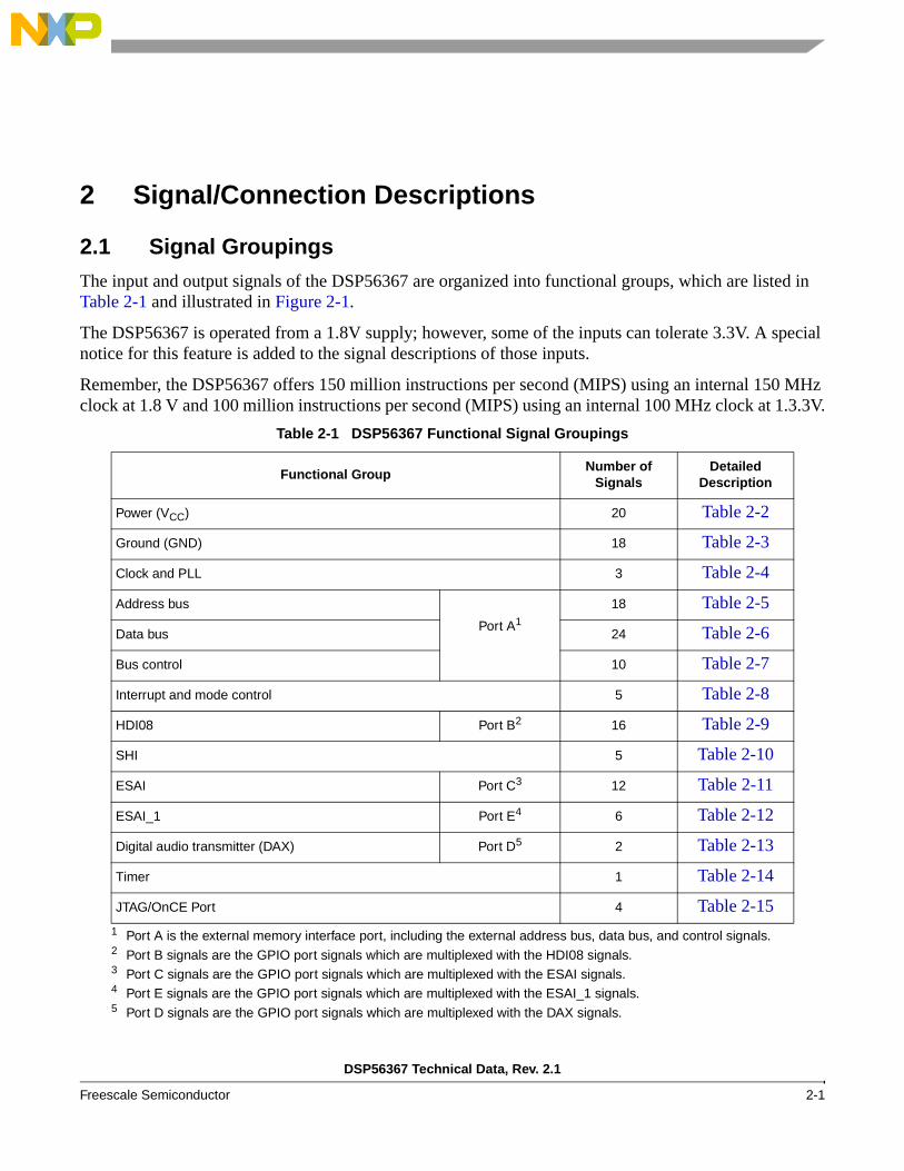
2 Signal/Connection Descriptions
2.1 Signal GroupingsThe input and output signals of the DSP56367 are organized into functional groups, which are listed in Table 2-1 and illustrated in Figure 2-1.
The DSP56367 is operated from a 1.8V supply; however, some of the inputs can tolerate 3.3V. A special notice for this feature is added to the signal descriptions of those inputs.
Remember, the DSP56367 offers 150 million instructions per second (MIPS) using an internal 150 MHz clock at 1.8 V and 100 million instructions per second (MIPS) using an internal 100 MHz clock at 1.3.3V.
Table 2-1 DSP56367 Functional Signal Groupings
Functional Group Number of Signals
Detailed Description
Power (VCC) 20 Table 2-2
Ground (GND) 18 Table 2-3
Clock and PLL 3 Table 2-4
Address bus
Port A1
1 Port A is the external memory interface port, including the external address bus, data bus, and control signals.
18 Table 2-5
Data bus 24 Table 2-6
Bus control 10 Table 2-7
Interrupt and mode control 5 Table 2-8
HDI08 Port B2
2 Port B signals are the GPIO port signals which are multiplexed with the HDI08 signals.
16 Table 2-9
SHI 5 Table 2-10
ESAI Port C3
3 Port C signals are the GPIO port signals which are multiplexed with the ESAI signals.
12 Table 2-11
ESAI_1 Port E4
4 Port E signals are the GPIO port signals which are multiplexed with the ESAI_1 signals.
6 Table 2-12
Digital audio transmitter (DAX) Port D5
5 Port D signals are the GPIO port signals which are multiplexed with the DAX signals.
2 Table 2-13
Timer 1 Table 2-14
JTAG/OnCE Port 4 Table 2-15

Signal Groupings
DSP56367 Technical Data, Rev. 2.1
2-2 Freescale Semiconductor
Figure 2-1 Signals Identified by Functional Group
PORT A ADDRESS BUS
A0-A17VCCA (3)
GNDA (4)
D0-D23VCCD (4)GNDD (4)
AA0-AA2/RAS0-RAS2
PORT A BUS CONTROL
PORT A DATA BUS
OnCE‰ ON-CHIP EMULATION/
TCKTDO
VCCH GNDH
VCCQL (4)
Port B
Port C
JTAG PORT
PINIT/NMI
VCCQH (3)
VCCC (2)GNDC (2)
INTERRUPT AND MODE CONTROL
MODA/IRQAMODB/IRQBMODC/IRQCMODD/IRQD
RESET
PLL AND CLOCK
EXTAL
PCAP
GNDPVCCP
Port D
QUIET POWER
GNDQ (4)
SPDIF TRANSMITTER (DAX)ADO [PD1]ACI [PD0]
TIMER 0 TIO0 [TIO0]
HREQSCK/SCL
MISO/SDASS/HA2MOSI/HA0
TMSPARALLEL HOST PORT (HDI08)
DSP56367
HAD(7:0) [PB0-PB7]HAS/HA0 [PB8]HA8/HA1 [PB9]HA9/HA2 [PB10]HRW/HRD [PB11]HDS/HWR [PB12]HCS/HA10 [PB13]HOREQ/HTRQ [PB14]HACK/HRRQ [PB15]
SERIAL AUDIO INTERFACE (ESAI)
TDI
SERIAL HOST INTERFACE (SHI)GNDS (2)VCCS (2)
FST [PC4]HCKT [PC5]SCKR [PC0]FSR [PC1]HCKR [PC2]SDO0[PC11] / SDO0_1[PE11]SDO1[PC10] / SDO1_1[PE10]SDO2/SDI3[PC9] / SDO2_1/SDI3_1[PE9]SDO3/SDI2[PC8] / SDO3_1/SDI2_1[PE8]SDO4/SDI1 [PC7]SDO5/SDI0 [PC6]
FSSCKT_1[PE3]
SCKT[PC3]
T_1[PE4]SCKR_1[PE0]FSR_1[PE1]SDO4_1/SDI1_1[PE7]SDO5_1/SDI0_1[PE6]
BBBGBRTAWRRD
CAS
Port E
SERIAL AUDIO INTERFACE(ESAI_1)

Power
DSP56367 Technical Data, Rev. 2.1
Freescale Semiconductor 2-3
2.2 Power
2.3 Ground
Table 2-2 Power Inputs
Power Name Description
VCCP PLL Power—VCCP is VCC dedicated for PLL use. The voltage should be well-regulated and the input should be provided with an extremely low impedance path to the VCC power rail. There is one VCCP input.
VCCQL (4) Quiet Core (Low) Power—VCCQL is an isolated power for the internal processing logic. This input must be tied externally to all other VCCQL power pins and the VCCP power pin only. Do not tie with other power pins. The user must provide adequate external decoupling capacitors. There are four VCCQL inputs.
VCCQH (3) Quiet External (High) Power—VCCQH is a quiet power source for I/O lines. This input must be tied externally to all other chip power inputs.The user must provide adequate decoupling capacitors. There are three VCCQH inputs.
VCCA (3) Address Bus Power—VCCA is an isolated power for sections of the address bus I/O drivers. This input must be tied externally to all other chip power inputs. The user must provide adequate external decoupling capacitors. There are three VCCA inputs.
VCCD (4) Data Bus Power—VCCD is an isolated power for sections of the data bus I/O drivers. This input must be tied externally to all other chip power inputs. The user must provide adequate external decoupling capacitors. There are four VCCD inputs.
VCCC (2) Bus Control Power—VCCC is an isolated power for the bus control I/O drivers. This input must be tied externally to all other chip power inputs. The user must provide adequate external decoupling capacitors. There are two VCCC inputs.
VCCH Host Power—VCCH is an isolated power for the HDI08 I/O drivers. This input must be tied externally to all other chip power inputs. The user must provide adequate external decoupling capacitors. There is one VCCH input.
VCCS (2) SHI, ESAI, ESAI_1, DAX and Timer Power —VCCS is an isolated power for the SHI, ESAI, ESAI_1, DAX and Timer. This input must be tied externally to all other chip power inputs. The user must provide adequate external decoupling capacitors. There are two VCCS inputs.
Table 2-3 Grounds
Ground Name Description
GNDP PLL Ground—GNDP is a ground dedicated for PLL use. The connection should be provided with an extremely low-impedance path to ground. VCCP should be bypassed to GNDP by a 0.47 µF capacitor located as close as possible to the chip package. There is one GNDP connection.
GNDQ (4) Quiet Ground—GNDQ is an isolated ground for the internal processing logic. This connection must be tied externally to all other chip ground connections. The user must provide adequate external decoupling capacitors. There are four GNDQ connections.
GNDA (4) Address Bus Ground—GNDA is an isolated ground for sections of the address bus I/O drivers. This connection must be tied externally to all other chip ground connections. The user must provide adequate external decoupling capacitors. There are four GNDA connections.
GNDD (4) Data Bus Ground—GNDD is an isolated ground for sections of the data bus I/O drivers. This connection must be tied externally to all other chip ground connections. The user must provide adequate external decoupling capacitors. There are four GNDD connections.

Clock and PLL
DSP56367 Technical Data, Rev. 2.1
2-4 Freescale Semiconductor
2.4 Clock and PLL
2.5 External Memory Expansion Port (Port A) When the DSP56367 enters a low-power standby mode (stop or wait), it releases bus mastership and tri-states the relevant port A signals: A0–A17, D0–D23, AA0/RAS0–AA2/RAS2, RD, WR, BB, CAS.
2.6 External Address Bus
GNDC (2) Bus Control Ground—GNDC is an isolated ground for the bus control I/O drivers. This connection must be tied externally to all other chip ground connections. The user must provide adequate external decoupling capacitors. There are two GNDC connections.
GNDH Host Ground—GNDh is an isolated ground for the HD08 I/O drivers. This connection must be tied externally to all other chip ground connections. The user must provide adequate external decoupling capacitors. There is one GNDH connection.
GNDS (2) SHI, ESAI, ESAI_1, DAX and Timer Ground—GNDS is an isolated ground for the SHI, ESAI, ESAI_1, DAX and Timer. This connection must be tied externally to all other chip ground connections. The user must provide adequate external decoupling capacitors. There are two GNDS connections.
Table 2-4 Clock and PLL Signals
Signal Name Type State During Reset Signal Description
EXTAL Input Input External Clock Input—An external clock source must be connected to EXTAL in order to supply the clock to the internal clock generator and PLL.
PCAP Input Input PLL Capacitor—PCAP is an input connecting an off-chip capacitor to the PLL filter. Connect one capacitor terminal to PCAP and the other terminal to VCCP.
If the PLL is not used, PCAP may be tied to VCC, GND, or left floating.
PINIT/NMI Input Input PLL Initial/Nonmaskable Interrupt—During assertion of RESET, the value of PINIT/NMI is written into the PLL Enable (PEN) bit of the PLL control register, determining whether the PLL is enabled or disabled. After RESET de assertion and during normal instruction processing, the PINIT/NMI Schmitt-trigger input is a negative-edge-triggered nonmaskable interrupt (NMI) request internally synchronized to internal system clock.
Table 2-5 External Address Bus Signals
Signal Name Type State During Reset Signal Description
A0–A17 Output Tri-Stated Address Bus—When the DSP is the bus master, A0–A17 are active-high outputs that specify the address for external program and data memory accesses. Otherwise, the signals are tri-stated. To minimize power dissipation, A0–A17 do not change state when external memory spaces are not being accessed.
Table 2-3 Grounds (continued)
Ground Name Description

External Data Bus
DSP56367 Technical Data, Rev. 2.1
Freescale Semiconductor 2-5
2.7 External Data Bus
2.8 External Bus Control
Table 2-6 External Data Bus Signals
Signal Name Type State during Reset Signal Description
D0–D23 Input/Output Tri-Stated Data Bus—When the DSP is the bus master, D0–D23 are active-high, bidirectional input/outputs that provide the bidirectional data bus for external program and data memory accesses. Otherwise, D0–D23 are tri-stated.
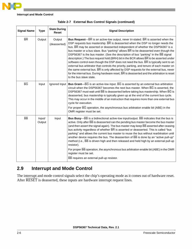
Table 2-7 External Bus Control Signals
Signal Name Type State During Reset Signal Description
AA0–AA2/RAS0–RAS2
Output Tri-Stated Address Attribute or Row Address Strobe—When defined as AA, these signals can be used as chip selects or additional address lines. When defined as RAS, these signals can be used as RAS for DRAM interface. These signals are tri-statable outputs with programmable polarity.
CAS Output Tri-Stated Column Address Strobe— When the DSP is the bus master, CAS is an active-low output used by DRAM to strobe the column address. Otherwise, if the bus mastership enable (BME) bit in the DRAM control register is cleared, the signal is tri-stated.
RD Output Tri-Stated Read Enable—When the DSP is the bus master, RD is an active-low output that is asserted to read external memory on the data bus (D0-D23). Otherwise, RD is tri-stated.
WR Output Tri-Stated Write Enable—When the DSP is the bus master, WR is an active-low output that is asserted to write external memory on the data bus (D0-D23). Otherwise, WR is tri-stated.
TA Input Ignored Input Transfer Acknowledge—If the DSP is the bus master and there is no external bus activity, or the DSP is not the bus master, the TA input is ignored. The TA input is a data transfer acknowledge (DTACK) function that can extend an external bus cycle indefinitely. Any number of wait states (1, 2. . .infinity) may be added to the wait states inserted by the BCR by keeping TA deasserted. In typical operation, TA is deasserted at the start of a bus cycle, is asserted to enable completion of the bus cycle, and is deasserted before the next bus cycle. The current bus cycle completes one clock period after TA is asserted synchronous to the internal system clock. The number of wait states is determined by the TA input or by the bus control register (BCR), whichever is longer. The BCR can be used to set the minimum number of wait states in external bus cycles.
In order to use the TA functionality, the BCR must be programmed to at least one wait state. A zero wait state access cannot be extended by TA deassertion, otherwise improper operation may result. TA can operate synchronously or asynchronously, depending on the setting of the TAS bit in the operating mode register (OMR).
TA functionality may not be used while performing DRAM type accesses, otherwise improper operation may result.
Interrupt and Mode Control
DSP56367 Technical Data, Rev. 2.1
2-6 Freescale Semiconductor
2.9 Interrupt and Mode ControlThe interrupt and mode control signals select the chip’s operating mode as it comes out of hardware reset. After RESET is deasserted, these inputs are hardware interrupt request lines.
BR Output Output
(deasserted)
Bus Request—BR is an active-low output, never tri-stated. BR is asserted when the DSP requests bus mastership. BR is deasserted when the DSP no longer needs the bus. BR may be asserted or deasserted independent of whether the DSP56367 is a bus master or a bus slave. Bus “parking” allows BR to be deasserted even though the DSP56367 is the bus master. (See the description of bus “parking” in the BB signal description.) The bus request hold (BRH) bit in the BCR allows BR to be asserted under software control even though the DSP does not need the bus. BR is typically sent to an external bus arbitrator that controls the priority, parking, and tenure of each master on the same external bus. BR is only affected by DSP requests for the external bus, never for the internal bus. During hardware reset, BR is deasserted and the arbitration is reset to the bus slave state.
BG Input Ignored Input Bus Grant—BG is an active-low input. BG is asserted by an external bus arbitration circuit when the DSP56367 becomes the next bus master. When BG is asserted, the DSP56367 must wait until BB is deasserted before taking bus mastership. When BG is deasserted, bus mastership is typically given up at the end of the current bus cycle. This may occur in the middle of an instruction that requires more than one external bus cycle for execution.
For proper BG operation, the asynchronous bus arbitration enable bit (ABE) in the OMR register must be set.
BB Input/Output
Input Bus Busy—BB is a bidirectional active-low input/output. BB indicates that the bus is active. Only after BB is deasserted can the pending bus master become the bus master (and then assert the signal again). The bus master may keep BB asserted after ceasing bus activity regardless of whether BR is asserted or deasserted. This is called “bus parking” and allows the current bus master to reuse the bus without rearbitration until another device requires the bus. The deassertion of BB is done by an “active pull-up” method (i.e., BB is driven high and then released and held high by an external pull-up resistor).
For proper BB operation, the asynchronous bus arbitration enable bit (ABE) in the OMR register must be set.
BB requires an external pull-up resistor.
Table 2-7 External Bus Control Signals (continued)
Signal Name Type State During Reset Signal Description
Interrupt and Mode Control
DSP56367 Technical Data, Rev. 2.1
Freescale Semiconductor 2-7
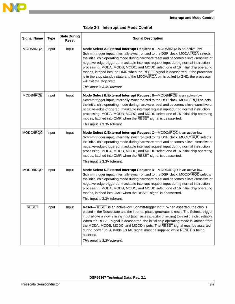
Table 2-8 Interrupt and Mode Control
Signal Name Type State During Reset Signal Description
MODA/IRQA Input Input Mode Select A/External Interrupt Request A—MODA/IRQA is an active-low Schmitt-trigger input, internally synchronized to the DSP clock. MODA/IRQA selects the initial chip operating mode during hardware reset and becomes a level-sensitive or negative-edge-triggered, maskable interrupt request input during normal instruction processing. MODA, MODB, MODC, and MODD select one of 16 initial chip operating modes, latched into the OMR when the RESET signal is deasserted. If the processor is in the stop standby state and the MODA/IRQA pin is pulled to GND, the processor will exit the stop state.
This input is 3.3V tolerant.
MODB/IRQB Input Input Mode Select B/External Interrupt Request B—MODB/IRQB is an active-low Schmitt-trigger input, internally synchronized to the DSP clock. MODB/IRQB selects the initial chip operating mode during hardware reset and becomes a level-sensitive or negative-edge-triggered, maskable interrupt request input during normal instruction processing. MODA, MODB, MODC, and MODD select one of 16 initial chip operating modes, latched into OMR when the RESET signal is deasserted.
This input is 3.3V tolerant.
MODC/IRQC Input Input Mode Select C/External Interrupt Request C—MODC/IRQC is an active-low Schmitt-trigger input, internally synchronized to the DSP clock. MODC/IRQC selects the initial chip operating mode during hardware reset and becomes a level-sensitive or negative-edge-triggered, maskable interrupt request input during normal instruction processing. MODA, MODB, MODC, and MODD select one of 16 initial chip operating modes, latched into OMR when the RESET signal is deasserted.
This input is 3.3V tolerant.
MODD/IRQD Input Input Mode Select D/External Interrupt Request D—MODD/IRQD is an active-low Schmitt-trigger input, internally synchronized to the DSP clock. MODD/IRQD selects the initial chip operating mode during hardware reset and becomes a level-sensitive or negative-edge-triggered, maskable interrupt request input during normal instruction processing. MODA, MODB, MODC, and MODD select one of 16 initial chip operating modes, latched into OMR when the RESET signal is deasserted.
This input is 3.3V tolerant.
RESET Input Input Reset—RESET is an active-low, Schmitt-trigger input. When asserted, the chip is placed in the Reset state and the internal phase generator is reset. The Schmitt-trigger input allows a slowly rising input (such as a capacitor charging) to reset the chip reliably. When the RESET signal is deasserted, the initial chip operating mode is latched from the MODA, MODB, MODC, and MODD inputs. The RESET signal must be asserted during power up. A stable EXTAL signal must be supplied while RESET is being asserted.
This input is 3.3V tolerant.

Parallel Host Interface (HDI08)
DSP56367 Technical Data, Rev. 2.1
2-8 Freescale Semiconductor
2.10 Parallel Host Interface (HDI08) The HDI08 provides a fast, 8-bit, parallel data port that may be connected directly to the host bus. The HDI08 supports a variety of standard buses and can be directly connected to a number of industry standard microcomputers, microprocessors, DSPs, and DMA hardware.
Table 2-9 Host Interface
Signal Name Type State During Reset Signal Description
H0–H7
HAD0–HAD7
PB0–PB7
Input/Output
Input/Output
Input, Output, or Disconnected
GPIO Disconnected
Host Data—When HDI08 is programmed to interface a nonmultiplexed host bus and the HI function is selected, these signals are lines 0–7 of the bidirectional, tri-state data bus.
Host Address/Data—When HDI08 is programmed to interface a multiplexed host bus and the HI function is selected, these signals are lines 0–7 of the address/data bidirectional, multiplexed, tri-state bus.
Port B 0–7—When the HDI08 is configured as GPIO, these signals are individually programmable as input, output, or internally disconnected.
The default state after reset for these signals is GPIO disconnected.
These inputs are 3.3V tolerant.
HA0
HAS/HAS
PB8
Input
Input
Input, Output, or Disconnected
GPIO Disconnected
Host Address Input 0—When the HDI08 is programmed to interface a nonmultiplexed host bus and the HI function is selected, this signal is line 0 of the host address input bus.
Host Address Strobe—When HDI08 is programmed to interface a multiplexed host bus and the HI function is selected, this signal is the host address strobe (HAS) Schmitt-trigger input. The polarity of the address strobe is programmable, but is configured active-low (HAS) following reset.
Port B 8—When the HDI08 is configured as GPIO, this signal is individually programmed as input, output, or internally disconnected.
The default state after reset for this signal is GPIO disconnected.
This input is 3.3V tolerant.
HA1
HA8
PB9
Input
Input
Input, Output, or Disconnected
GPIO Disconnected
Host Address Input 1—When the HDI08 is programmed to interface a nonmultiplexed host bus and the HI function is selected, this signal is line 1 of the host address (HA1) input bus.
Host Address 8—When HDI08 is programmed to interface a multiplexed host bus and the HI function is selected, this signal is line 8 of the host address (HA8) input bus.
Port B 9—When the HDI08 is configured as GPIO, this signal is individually programmed as input, output, or internally disconnected.
The default state after reset for this signal is GPIO disconnected.
This input is 3.3V tolerant.

Parallel Host Interface (HDI08)
DSP56367 Technical Data, Rev. 2.1
Freescale Semiconductor 2-9
HA2
HA9
PB10
Input
Input
Input, Output, or Disconnected
GPIO Disconnected
Host Address Input 2—When the HDI08 is programmed to interface a non-multiplexed host bus and the HI function is selected, this signal is line 2 of the host address (HA2) input bus.
Host Address 9—When HDI08 is programmed to interface a multiplexed host bus and the HI function is selected, this signal is line 9 of the host address (HA9) input bus.
Port B 10—When the HDI08 is configured as GPIO, this signal is individually programmed as input, output, or internally disconnected.
The default state after reset for this signal is GPIO disconnected.
This input is 3.3V tolerant.
HRW
HRD/HRD
PB11
Input
Input
Input, Output, or Disconnected
GPIO Disconnected
Host Read/Write—When HDI08 is programmed to interface a single-data-strobe host bus and the HI function is selected, this signal is the Host Read/Write (HRW) input.
Host Read Data—When HDI08 is programmed to interface a double-data-strobe host bus and the HI function is selected, this signal is the host read data strobe (HRD) Schmitt-trigger input. The polarity of the data strobe is programmable, but is configured as active-low (HRD) after reset.
Port B 11—When the HDI08 is configured as GPIO, this signal is individually programmed as input, output, or internally disconnected.
The default state after reset for this signal is GPIO disconnected.
This input is 3.3V tolerant.
HDS/HDS
HWR/HWR
PB12
Input
Input
Input, Output, or Disconnected
GPIO Disconnected
Host Data Strobe—When HDI08 is programmed to interface a single-data-strobe host bus and the HI function is selected, this signal is the host data strobe (HDS) Schmitt-trigger input. The polarity of the data strobe is programmable, but is configured as active-low (HDS) following reset.
Host Write Data—When HDI08 is programmed to interface a double-data-strobe host bus and the HI function is selected, this signal is the host write data strobe (HWR) Schmitt-trigger input. The polarity of the data strobe is programmable, but is configured as active-low (HWR) following reset.
Port B 12—When the HDI08 is configured as GPIO, this signal is individually programmed as input, output, or internally disconnected.
The default state after reset for this signal is GPIO disconnected.
This input is 3.3V tolerant.
Table 2-9 Host Interface (continued)
Signal Name Type State During Reset Signal Description

Parallel Host Interface (HDI08)
DSP56367 Technical Data, Rev. 2.1
2-10 Freescale Semiconductor
HCS
HA10
PB13
Input
Input
Input, Output, or Disconnected
GPIO Disconnected
Host Chip Select—When HDI08 is programmed to interface a nonmultiplexed host bus and the HI function is selected, this signal is the host chip select (HCS) input. The polarity of the chip select is programmable, but is configured active-low (HCS) after reset.
Host Address 10—When HDI08 is programmed to interface a multiplexed host bus and the HI function is selected, this signal is line 10 of the host address (HA10) input bus.
Port B 13—When the HDI08 is configured as GPIO, this signal is individually programmed as input, output, or internally disconnected.
The default state after reset for this signal is GPIO disconnected.
This input is 3.3V tolerant.
HOREQ/HOREQ
HTRQ/HTRQ
PB14
Output
Output
Input, Output, or Disconnected
GPIO Disconnected
Host Request—When HDI08 is programmed to interface a single host request host bus and the HI function is selected, this signal is the host request (HOREQ) output. The polarity of the host request is programmable, but is configured as active-low (HOREQ) following reset. The host request may be programmed as a driven or open-drain output.
Transmit Host Request—When HDI08 is programmed to interface a double host request host bus and the HI function is selected, this signal is the transmit host request (HTRQ) output. The polarity of the host request is programmable, but is configured as active-low (HTRQ) following reset. The host request may be programmed as a driven or open-drain output.
Port B 14—When the HDI08 is configured as GPIO, this signal is individually programmed as input, output, or internally disconnected.
The default state after reset for this signal is GPIO disconnected.
This input is 3.3V tolerant.
HACK/HACK
HRRQ/HRRQ
PB15
Input
Output
Input, Output, or Disconnected
GPIO Disconnected
Host Acknowledge—When HDI08 is programmed to interface a single host request host bus and the HI function is selected, this signal is the host acknowledge (HACK) Schmitt-trigger input. The polarity of the host acknowledge is programmable, but is configured as active-low (HACK) after reset.
Receive Host Request—When HDI08 is programmed to interface a double host request host bus and the HI function is selected, this signal is the receive host request (HRRQ) output. The polarity of the host request is programmable, but is configured as active-low (HRRQ) after reset. The host request may be programmed as a driven or open-drain output.
Port B 15—When the HDI08 is configured as GPIO, this signal is individually programmed as input, output, or internally disconnected.
The default state after reset for this signal is GPIO disconnected.
This input is 3.3V tolerant.
Table 2-9 Host Interface (continued)
Signal Name Type State During Reset Signal Description

Serial Host Interface
DSP56367 Technical Data, Rev. 2.1
Freescale Semiconductor 2-11
2.11 Serial Host Interface The SHI has five I/O signals that can be configured to allow the SHI to operate in either SPI or I2C mode.
Table 2-10 Serial Host Interface Signals
Signal Name
Signal Type
State During Reset Signal Description
SCK
SCL
Input or Output
Input or Output
Tri-Stated SPI Serial Clock—The SCK signal is an output when the SPI is configured as a master and a Schmitt-trigger input when the SPI is configured as a slave. When the SPI is configured as a master, the SCK signal is derived from the internal SHI clock generator. When the SPI is configured as a slave, the SCK signal is an input, and the clock signal from the external master synchronizes the data transfer. The SCK signal is ignored by the SPI if it is defined as a slave and the slave select (SS) signal is not asserted. In both the master and slave SPI devices, data is shifted on one edge of the SCK signal and is sampled on the opposite edge where data is stable. Edge polarity is determined by the SPI transfer protocol.
I2C Serial Clock—SCL carries the clock for I2C bus transactions in the I2C mode. SCL is a Schmitt-trigger input when configured as a slave and an open-drain output when configured as a master. SCL should be connected to VCC through a pull-up resistor.
This signal is tri-stated during hardware, software, and individual reset. Thus, there is no need for an external pull-up in this state.
This input is 3.3V tolerant.
MISO
SDA
Input or Output
Input or Open-Drain
Output
Tri-Stated SPI Master-In-Slave-Out—When the SPI is configured as a master, MISO is the master data input line. The MISO signal is used in conjunction with the MOSI signal for transmitting and receiving serial data. This signal is a Schmitt-trigger input when configured for the SPI Master mode, an output when configured for the SPI Slave mode, and tri-stated if configured for the SPI Slave mode when SS is deasserted. An external pull-up resistor is not required for SPI operation.
I2C Data and Acknowledge—In I2C mode, SDA is a Schmitt-trigger input when receiving and an open-drain output when transmitting. SDA should be connected to VCC through a pull-up resistor. SDA carries the data for I2C transactions. The data in SDA must be stable during the high period of SCL. The data in SDA is only allowed to change when SCL is low. When the bus is free, SDA is high. The SDA line is only allowed to change during the time SCL is high in the case of start and stop events. A high-to-low transition of the SDA line while SCL is high is a unique situation, and is defined as the start event. A low-to-high transition of SDA while SCL is high is a unique situation defined as the stop event.
This signal is tri-stated during hardware, software, and individual reset. Thus, there is no need for an external pull-up in this state.
This input is 3.3V tolerant.

Serial Host Interface
DSP56367 Technical Data, Rev. 2.1
2-12 Freescale Semiconductor
MOSI
HA0
Input or Output
Input
Tri-Stated SPI Master-Out-Slave-In—When the SPI is configured as a master, MOSI is the master data output line. The MOSI signal is used in conjunction with the MISO signal for transmitting and receiving serial data. MOSI is the slave data input line when the SPI is configured as a slave. This signal is a Schmitt-trigger input when configured for the SPI Slave mode.
I2C Slave Address 0—This signal uses a Schmitt-trigger input when configured for the I2C mode. When configured for I2C slave mode, the HA0 signal is used to form the slave device address. HA0 is ignored when configured for the I2C master mode.
This signal is tri-stated during hardware, software, and individual reset. Thus, there is no need for an external pull-up in this state.
This input is 3.3V tolerant.
SS
HA2
Input
Input
Tri-Stated SPI Slave Select—This signal is an active low Schmitt-trigger input when configured for the SPI mode. When configured for the SPI Slave mode, this signal is used to enable the SPI slave for transfer. When configured for the SPI master mode, this signal should be kept deasserted (pulled high). If it is asserted while configured as SPI master, a bus error condition is flagged. If SS is deasserted, the SHI ignores SCK clocks and keeps the MISO output signal in the high-impedance state.
I2C Slave Address 2—This signal uses a Schmitt-trigger input when configured for the I2C mode. When configured for the I2C Slave mode, the HA2 signal is used to form the slave device address. HA2 is ignored in the I2C master mode.
This signal is tri-stated during hardware, software, and individual reset. Thus, there is no need for an external pull-up in this state.
This input is 3.3V tolerant.
HREQ Input or Output
Tri-Stated Host Request—This signal is an active low Schmitt-trigger input when configured for the master mode but an active low output when configured for the slave mode.
When configured for the slave mode, HREQ is asserted to indicate that the SHI is ready for the next data word transfer and deasserted at the first clock pulse of the new data word transfer. When configured for the master mode, HREQ is an input. When asserted by the external slave device, it will trigger the start of the data word transfer by the master. After finishing the data word transfer, the master will await the next assertion of HREQ to proceed to the next transfer.
This signal is tri-stated during hardware, software, personal reset, or when the HREQ1–HREQ0 bits in the HCSR are cleared. There is no need for external pull-up in this state.
This input is 3.3V tolerant.
Table 2-10 Serial Host Interface Signals (continued)
Signal Name
Signal Type
State During Reset Signal Description
Enhanced Serial Audio Interface
DSP56367 Technical Data, Rev. 2.1
Freescale Semiconductor 2-13
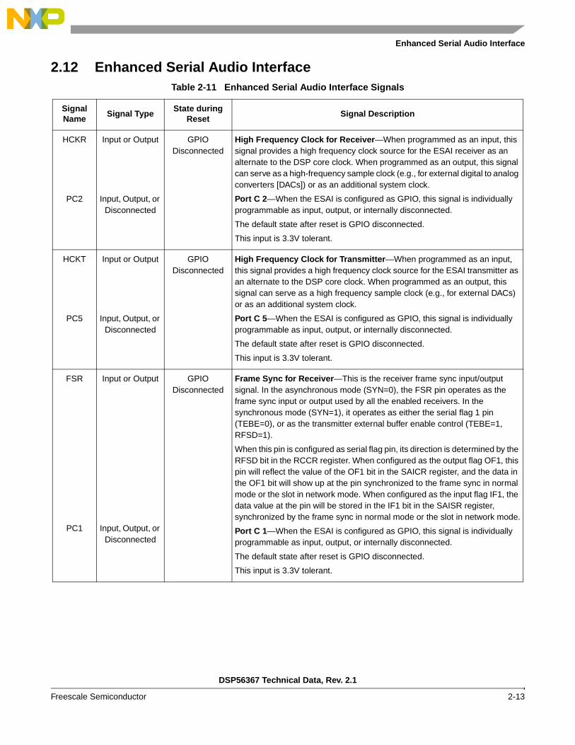
2.12 Enhanced Serial Audio Interface Table 2-11 Enhanced Serial Audio Interface Signals
Signal Name Signal Type State during
Reset Signal Description
HCKR
PC2
Input or Output
Input, Output, or Disconnected
GPIO Disconnected
High Frequency Clock for Receiver—When programmed as an input, this signal provides a high frequency clock source for the ESAI receiver as an alternate to the DSP core clock. When programmed as an output, this signal can serve as a high-frequency sample clock (e.g., for external digital to analog converters [DACs]) or as an additional system clock.
Port C 2—When the ESAI is configured as GPIO, this signal is individually programmable as input, output, or internally disconnected.
The default state after reset is GPIO disconnected.
This input is 3.3V tolerant.
HCKT
PC5
Input or Output
Input, Output, or Disconnected
GPIO Disconnected
High Frequency Clock for Transmitter—When programmed as an input, this signal provides a high frequency clock source for the ESAI transmitter as an alternate to the DSP core clock. When programmed as an output, this signal can serve as a high frequency sample clock (e.g., for external DACs) or as an additional system clock.
Port C 5—When the ESAI is configured as GPIO, this signal is individually programmable as input, output, or internally disconnected.
The default state after reset is GPIO disconnected.
This input is 3.3V tolerant.
FSR
PC1
Input or Output
Input, Output, or Disconnected
GPIO Disconnected
Frame Sync for Receiver—This is the receiver frame sync input/output signal. In the asynchronous mode (SYN=0), the FSR pin operates as the frame sync input or output used by all the enabled receivers. In the synchronous mode (SYN=1), it operates as either the serial flag 1 pin (TEBE=0), or as the transmitter external buffer enable control (TEBE=1, RFSD=1).
When this pin is configured as serial flag pin, its direction is determined by the RFSD bit in the RCCR register. When configured as the output flag OF1, this pin will reflect the value of the OF1 bit in the SAICR register, and the data in the OF1 bit will show up at the pin synchronized to the frame sync in normal mode or the slot in network mode. When configured as the input flag IF1, the data value at the pin will be stored in the IF1 bit in the SAISR register, synchronized by the frame sync in normal mode or the slot in network mode.
Port C 1—When the ESAI is configured as GPIO, this signal is individually programmable as input, output, or internally disconnected.
The default state after reset is GPIO disconnected.
This input is 3.3V tolerant.

Enhanced Serial Audio Interface
DSP56367 Technical Data, Rev. 2.1
2-14 Freescale Semiconductor
FST
PC4
Input or Output
Input, Output, or Disconnected
GPIO Disconnected
Frame Sync for Transmitter—This is the transmitter frame sync input/output signal. For synchronous mode, this signal is the frame sync for both transmitters and receivers. For asynchronous mode, FST is the frame sync for the transmitters only. The direction is determined by the transmitter frame sync direction (TFSD) bit in the ESAI transmit clock control register (TCCR).
Port C 4—When the ESAI is configured as GPIO, this signal is individually programmable as input, output, or internally disconnected.
The default state after reset is GPIO disconnected.
This input is 3.3V tolerant.
SCKR
PC0
Input or Output
Input, Output, or Disconnected
GPIO Disconnected
Receiver Serial Clock—SCKR provides the receiver serial bit clock for the ESAI. The SCKR operates as a clock input or output used by all the enabled receivers in the asynchronous mode (SYN=0), or as serial flag 0 pin in the synchronous mode (SYN=1).
When this pin is configured as serial flag pin, its direction is determined by the RCKD bit in the RCCR register. When configured as the output flag OF0, this pin will reflect the value of the OF0 bit in the SAICR register, and the data in the OF0 bit will show up at the pin synchronized to the frame sync in normal mode or the slot in network mode. When configured as the input flag IF0, the data value at the pin will be stored in the IF0 bit in the SAISR register, synchronized by the frame sync in normal mode or the slot in network mode.
Port C 0—When the ESAI is configured as GPIO, this signal is individually programmable as input, output, or internally disconnected.
The default state after reset is GPIO disconnected.
This input is 3.3V tolerant.
SCKT
PC3
Input or output
Input, Output, or Disconnected
GPIO Disconnected
Transmitter Serial Clock—This signal provides the serial bit rate clock for the ESAI. SCKT is a clock input or output used by all enabled transmitters and receivers in synchronous mode, or by all enabled transmitters in asynchronous mode.
Port C 3—When the ESAI is configured as GPIO, this signal is individually programmable as input, output, or internally disconnected.
The default state after reset is GPIO disconnected.
This input is 3.3V tolerant.
SDO5
SDI0
PC6
Output
Input
Input, Output, or Disconnected
GPIO Disconnected
Serial Data Output 5—When programmed as a transmitter, SDO5 is used to transmit data from the TX5 serial transmit shift register.
Serial Data Input 0—When programmed as a receiver, SDI0 is used to receive serial data into the RX0 serial receive shift register.
Port C 6—When the ESAI is configured as GPIO, this signal is individually programmable as input, output, or internally disconnected.
The default state after reset is GPIO disconnected.
This input is 3.3V tolerant.
Table 2-11 Enhanced Serial Audio Interface Signals (continued)
Signal Name Signal Type State during
Reset Signal Description

Enhanced Serial Audio Interface
DSP56367 Technical Data, Rev. 2.1
Freescale Semiconductor 2-15
SDO4
SDI1
PC7
Output
Input
Input, Output, or Disconnected
GPIO Disconnected
Serial Data Output 4—When programmed as a transmitter, SDO4 is used to transmit data from the TX4 serial transmit shift register.
Serial Data Input 1—When programmed as a receiver, SDI1 is used to receive serial data into the RX1 serial receive shift register.
Port C 7—When the ESAI is configured as GPIO, this signal is individually programmable as input, output, or internally disconnected.
The default state after reset is GPIO disconnected.
This input is 3.3V tolerant.
SDO3/SDO3_1
SDI2/SDI2_1
PC8/PE8
Output
Input
Input, Output, or Disconnected
GPIO Disconnected
Serial Data Output 3—When programmed as a transmitter, SDO3 is used to transmit data from the TX3 serial transmit shift register.
When enabled for ESAI_1 operation, this is the ESAI_1 Serial Data Output 3.
Serial Data Input 2—When programmed as a receiver, SDI2 is used to receive serial data into the RX2 serial receive shift register.
When enabled for ESAI_1 operation, this is the ESAI_1 Serial Data Input 2.
Port C 8—When the ESAI is configured as GPIO, this signal is individually programmable as input, output, or internally disconnected.
When enabled for ESAI_1 GPIO, this is the Port E 8 signal.
The default state after reset is GPIO disconnected.
This input is 3.3V tolerant.
SDO2/SDO2_1
SDI3/SDI3_1
PC9/PE9
Output
Input
Input, Output, or Disconnected
GPIO Disconnected
Serial Data Output 2—When programmed as a transmitter, SDO2 is used to transmit data from the TX2 serial transmit shift register.
When enabled for ESAI_1 operation, this is the ESAI_1 Serial Data Output 2.
Serial Data Input 3—When programmed as a receiver, SDI3 is used to receive serial data into the RX3 serial receive shift register.
When enabled for ESAI_1 operation, this is the ESAI_1 Serial Data Input 3.
Port C 9—When the ESAI is configured as GPIO, this signal is individually programmable as input, output, or internally disconnected.
When enabled for ESAI_1 GPIO, this is the Port E 9 signal.
The default state after reset is GPIO disconnected.
This input is 3.3V tolerant.
SDO1/SDO1_1
PC10/PE10
Output
Input, Output, or disconnected
GPIO Disconnected
Serial Data Output 1—SDO1 is used to transmit data from the TX1 serial transmit shift register.
When enabled for ESAI_1 operation, this is the ESAI_1 Serial Data Output 1.
Port C 10—When the ESAI is configured as GPIO, this signal is individually programmable as input, output, or internally disconnected.
When enabled for ESAI_1 GPIO, this is the Port E 10 signal.
The default state after reset is GPIO disconnected.
This input is 3.3V tolerant.
Table 2-11 Enhanced Serial Audio Interface Signals (continued)
Signal Name Signal Type State during
Reset Signal Description

Enhanced Serial Audio Interface_1
DSP56367 Technical Data, Rev. 2.1
2-16 Freescale Semiconductor
2.13 Enhanced Serial Audio Interface_1
SDO0/SDO0_1
PC11/PE11
Output
Input, Output, or Disconnected
GPIO Disconnected
Serial Data Output 0—SDO0 is used to transmit data from the TX0 serial transmit shift register.
When enabled for ESAI_1 operation, this is the ESAI_1 Serial Data Output 0.
Port C 11—When the ESAI is configured as GPIO, this signal is individually programmable as input, output, or internally disconnected.
When enabled for ESAI_1 GPIO, this is the Port E 11 signal.
The default state after reset is GPIO disconnected.
This input is 3.3V tolerant.
Table 2-12 Enhanced Serial Audio Interface_1 Signals
Signal Name Signal Type State during
Reset Signal Description
FSR_1
PE1
Input or Output
Input, Output, or Disconnected
GPIO Disconnected
Frame Sync for Receiver_1—This is the receiver frame sync input/output signal. In the asynchronous mode (SYN=0), the FSR pin operates as the frame sync input or output used by all the enabled receivers. In the synchronous mode (SYN=1), it operates as either the serial flag 1 pin (TEBE=0), or as the transmitter external buffer enable control (TEBE=1, RFSD=1).
When this pin is configured as serial flag pin, its direction is determined by the RFSD bit in the RCCR register. When configured as the output flag OF1, this pin will reflect the value of the OF1 bit in the SAICR register, and the data in the OF1 bit will show up at the pin synchronized to the frame sync in normal mode or the slot in network mode. When configured as the input flag IF1, the data value at the pin will be stored in the IF1 bit in the SAISR register, synchronized by the frame sync in normal mode or the slot in network mode.
Port E 1—When the ESAI is configured as GPIO, this signal is individually programmable as input, output, or internally disconnected.
The default state after reset is GPIO disconnected.
This input cannot tolerate 3.3V.
FST_1
PE4
Input or Output
Input, Output, or Disconnected
GPIO Disconnected
Frame Sync for Transmitter_1—This is the transmitter frame sync input/output signal. For synchronous mode, this signal is the frame sync for both transmitters and receivers. For asynchronous mode, FST is the frame sync for the transmitters only. The direction is determined by the transmitter frame sync direction (TFSD) bit in the ESAI transmit clock control register (TCCR).
Port E 4—When the ESAI is configured as GPIO, this signal is individually programmable as input, output, or internally disconnected.
The default state after reset is GPIO disconnected.
This input cannot tolerate 3.3V.
Table 2-11 Enhanced Serial Audio Interface Signals (continued)
Signal Name Signal Type State during
Reset Signal Description

Enhanced Serial Audio Interface_1
DSP56367 Technical Data, Rev. 2.1
Freescale Semiconductor 2-17
SCKR_1
PE0
Input or Output
Input, Output, or Disconnected
GPIO Disconnected
Receiver Serial Clock_1—SCKR provides the receiver serial bit clock for the ESAI. The SCKR operates as a clock input or output used by all the enabled receivers in the asynchronous mode (SYN=0), or as serial flag 0 pin in the synchronous mode (SYN=1).
When this pin is configured as serial flag pin, its direction is determined by the RCKD bit in the RCCR register. When configured as the output flag OF0, this pin will reflect the value of the OF0 bit in the SAICR register, and the data in the OF0 bit will show up at the pin synchronized to the frame sync in normal mode or the slot in network mode. When configured as the input flag IF0, the data value at the pin will be stored in the IF0 bit in the SAISR register, synchronized by the frame sync in normal mode or the slot in network mode.
Port E 0—When the ESAI is configured as GPIO, this signal is individually programmable as input, output, or internally disconnected.
The default state after reset is GPIO disconnected.
This input cannot tolerate 3.3V.
SCKT_1
PE3
Input or Output
Input, Output, or Disconnected
GPIO Disconnected
Transmitter Serial Clock_1—This signal provides the serial bit rate clock for the ESAI. SCKT is a clock input or output used by all enabled transmitters and receivers in synchronous mode, or by all enabled transmitters in asynchronous mode.
Port E 3—When the ESAI is configured as GPIO, this signal is individually programmable as input, output, or internally disconnected.
The default state after reset is GPIO disconnected.
This input cannot tolerate 3.3V.
SDO5_1
SDI0_1
PE6
Output
Input
Input, Output, or Disconnected
GPIO Disconnected
Serial Data Output 5_1—When programmed as a transmitter, SDO5 is used to transmit data from the TX5 serial transmit shift register.
Serial Data Input 0_1—When programmed as a receiver, SDI0 is used to receive serial data into the RX0 serial receive shift register.
Port E 6—When the ESAI is configured as GPIO, this signal is individually programmable as input, output, or internally disconnected.
The default state after reset is GPIO disconnected.
This input cannot tolerate 3.3V.
SDO4_1
SDI1_1
PE7
Output
Input
Input, Output, or Disconnected
GPIO Disconnected
Serial Data Output 4_1—When programmed as a transmitter, SDO4 is used to transmit data from the TX4 serial transmit shift register.
Serial Data Input 1_1—When programmed as a receiver, SDI1 is used to receive serial data into the RX1 serial receive shift register.
Port E 7—When the ESAI is configured as GPIO, this signal is individually programmable as input, output, or internally disconnected.
The default state after reset is GPIO disconnected.
This input is 3.3V tolerant.
Table 2-12 Enhanced Serial Audio Interface_1 Signals (continued)
Signal Name Signal Type State during
Reset Signal Description

SPDIF Transmitter Digital Audio Interface
DSP56367 Technical Data, Rev. 2.1
2-18 Freescale Semiconductor
2.14 SPDIF Transmitter Digital Audio Interface
2.15 Timer
Table 2-13 Digital Audio Interface (DAX) Signals
Signal Name Type State During
Reset Signal Description
ACI
PD0
Input
Input, Output, or Disconnected
GPIO Disconnected
Audio Clock Input—This is the DAX clock input. When programmed to use an external clock, this input supplies the DAX clock. The external clock frequency must be 256, 384, or 512 times the audio sampling frequency (256 × Fs, 384 × Fs or 512 × Fs, respectively).
Port D 0—When the DAX is configured as GPIO, this signal is individually programmable as input, output, or internally disconnected.
The default state after reset is GPIO disconnected.
This input is 3.3V tolerant.
ADO
PD1
Output
Input, Output, or Disconnected
GPIO Disconnected
Digital Audio Data Output—This signal is an audio and non-audio output in the form of AES/EBU, CP340 and IEC958 data in a biphase mark format.
Port D 1—When the DAX is configured as GPIO, this signal is individually programmable as input, output, or internally disconnected.
The default state after reset is GPIO disconnected.
This input is 3.3V tolerant.
Table 2-14 Timer Signal
Signal Name Type State during
Reset Signal Description
TIO0 Input or Output Input Timer 0 Schmitt-Trigger Input/Output—When timer 0 functions as an external event counter or in measurement mode, TIO0 is used as input. When timer 0 functions in watchdog, timer, or pulse modulation mode, TIO0 is used as output.
The default mode after reset is GPIO input. This can be changed to output or configured as a timer input/output through the timer 0 control/status register (TCSR0). If TIO0 is not being used, it is recommended to either define it as GPIO output immediately at the beginning of operation or leave it defined as GPIO input but connected to Vcc through a pull-up resistor in order to ensure a stable logic level at this input.
This input is 3.3 V tolerant.

JTAG/OnCE Interface
DSP56367 Technical Data, Rev. 2.1
Freescale Semiconductor 2-19
2.16 JTAG/OnCE InterfaceTable 2-15 JTAG/OnCE Interface
Signal Name Signal Type State during
Reset Signal Description
TCK Input Input Test Clock—TCK is a test clock input signal used to synchronize the JTAG test logic. It has an internal pull-up resistor.
This input is 3.3V tolerant.
TDI Input Input Test Data Input—TDI is a test data serial input signal used for test instructions and data. TDI is sampled on the rising edge of TCK and has an internal pull-up resistor.
This input is 3.3V tolerant.
TDO Output Tri-Stated Test Data Output—TDO is a test data serial output signal used for test instructions and data. TDO is tri-statable and is actively driven in the shift-IR and shift-DR controller states. TDO changes on the falling edge of TCK.
TMS Input Input Test Mode Select—TMS is an input signal used to sequence the test controller’s state machine. TMS is sampled on the rising edge of TCK and has an internal pull-up resistor.
This input is 3.3V tolerant.
JTAG/OnCE Interface
DSP56367 Technical Data, Rev. 2.1
2-20 Freescale Semiconductor
NOTES
DSP56367 Technical Data, Rev. 2.1
Freescale Semiconductor 3-1
3 Specifications
3.1 IntroductionThe DSP56367 is a high density CMOS device with Transistor-Transistor Logic (TTL) compatible inputs and outputs.
NOTEThis document contains information on a new product. Specifications and information herein are subject to change without notice.
Finalized specifications may be published after further characterization and device qualifications are completed.
3.2 Maximum RatingsCAUTION
This device contains circuitry protecting against damage due to high static voltage or electrical fields. However, normal precautions should be taken to avoid exceeding maximum voltage ratings. Reliability of operation is enhanced if unused inputs are pulled to an appropriate logic voltage level (for example, either GND or VCC). The suggested value for a pull-up or pull-down resistor is 10 k�.
NOTEIn the calculation of timing requirements, adding a maximum value of one specification to a minimum value of another specification does not yield a reasonable sum. A maximum specification is calculated using a worst case variation of process parameter values in one direction. The minimum specification is calculated using the worst case for the same parameters in the opposite direction. Therefore, a “maximum” value for a specification will never occur in the same device that has a “minimum” value for another specification; adding a maximum to a minimum represents a condition that can never exist.

Thermal Characteristics
DSP56367 Technical Data, Rev. 2.1
3-2 Freescale Semiconductor
3.3 Thermal Characteristics
Table 3-1 Maximum Ratings
Rating1 Symbol Value1, 2
1 GND = 0 V, VCCP, VCCQL = 1.8 V ±5%, TJ = –40×C to +95×C, CL = 50 pFAll other VCC = 3.3 V ± 5%, TJ = –40×C to +95×C, CL = 50 pF
2 Absolute maximum ratings are stress ratings only, and functional operation at the maximum is not guaranteed. Stress beyond the maximum rating may affect device reliability or cause permanent damage to the device.
Unit
Supply Voltage VCCQL, VCCP �0.3 to + 2.0 V
VCCQH, VCCA, VCCD, VCCC, VCCH, VCCS, �0.3 to + 4.0 V
All “3.3V tolerant” input voltages VIN GND � 0.3 to VCC + 0.7 V
Current drain per pin excluding VCC and GND I 10 mA
Operating temperature range3
3 Temperatures below -0°C are qualified for consumer applications.
TJ �40 to + 95 °C
Storage temperature TSTG �55 to +125 °C
Table 3-2 Thermal Characteristics
Characteristic Symbol TQFP Value Unit
Natural Convection, Junction-to-ambient thermal resistance1,2
1 Junction temperature is a function of die size, on-chip power dissipation, package thermal resistance, mounting site (board) temperature, ambient temperature, air flow, power dissipation of other components on the board, and board thermal resistance.
2 Per SEMI G38-87 and JEDEC JESD51-2 with the single layer board horizontal.
R�JA or �JA 45.0 °C/W
Junction-to-case thermal resistance3
3 Thermal resistance between the die and the case top surface as measured by the cold plate method (MIL SPEC-883 Method 1012.1).
R�JC or �JC 10.0 °C/W
Natural Convection, Thermal characterization parameter4
4 Thermal characterization parameter indicating the temperature difference between package top and the junction temperature per JEDEC JESD51-2. When Greek letters are not available, the thermal characterization parameter is written as Psi-JT.
�JT 3.0 °C/W

DC Electrical Characteristics
DSP56367 Technical Data, Rev. 2.1
Freescale Semiconductor 3-3
3.4 DC Electrical CharacteristicsTable 3-3 DC Electrical Characteristics1
1 VCCQL = 1.8 V ± 5%, TJ = –40°C to +95°C, CL = 50 pFAll other VCC = 3.3 V ± 5%, TJ = –40°C to +95°C, CL = 50 pF
Characteristics Symbol Min Typ Max Unit
Supply voltages
• Core (VCCQL)
• PLL(VCCP)
VCC 1.71 1.8 1.89 V
Supply voltages
• VCCQH
• VCCA
• VCCD
• VCCC
• VCCH
• VCCS
VCC 3.14 3.3 3.46 V
Input high voltage
• D(0:23), BG, BB, TA, ESAI_1 (except SDO4_1)
• MOD2/IRQ2, RESET, PINIT/NMI and all JTAG/ESAI_1/Timer/HDI08/DAX/(only SDO4_1)/SHI(SPI mode)
• SHI(I2C mode)
• EXTAL
2 Refers to MODA/IRQA, MODB/IRQB, MODC/IRQC, and MODD/IRQD pins.
VIH
VIHP
VIHP
VIHX
2.0
2.0
1.5
0.8 × VCCQH
—
—
—
—
VCCQH
VCCQH + 03 max for both VIHP
VCCQH + 03 max for both VIHP
0.8 × VCCQH
V
Input low voltage
• D(0:23), BG, BB, TA, ESAI_1(except SDO4_1)
• MOD2/IRQ2, RESET, PINIT/NMI and all JTAG/ESAI/Timer/HDI08/DAX/ESAI_1(only SDO4_1)/SHI(SPI mode)
• SHI(I2C mode)
• EXTAL
VIL
VILP
VILP
VILX
–0.3
–0.3
–0.3
–0.3
—
—
—
—
0.8
0.8
0.3 x VCC
0.2 x VCCQH
V
Input leakage current IIN –10 — 10 µA
High impedance (off-state) input current (@ 2.4 V / 0.4 V) ITSI –10 — 10 µA
Output high voltage3 VOH 2.4 — — V
Output low voltage3 VOL — — 0.4 V
Internal supply current4 at internal clock of 150MHz
• In Normal mode
• In Wait mode
• In Stop mode5
ICCI
ICCW
ICCS
——
—
58.0
7.3
2.0
115
20
4
mA
PLL supply current — 1 2.5 mA
Input capacitance6 CIN — — 10 pF

AC Electrical Characteristics
DSP56367 Technical Data, Rev. 2.1
3-4 Freescale Semiconductor
3.5 AC Electrical CharacteristicsThe timing waveforms shown in the AC electrical characteristics section are tested with a VIL maximum of 0.4 V and a VIH minimum of 2.4 V for all pins except EXTAL. AC timing specifications, which are referenced to a device input signal, are measured in production with respect to the 50% point of the respective input signal’s transition. DSP56367 output levels are measured with the production test machine VOL and VOH reference levels set at 0.4 V and 2.4 V, respectively.
NOTEAlthough the minimum value for the frequency of EXTAL is 0 MHz, the device AC test conditions are 15 MHz and rated speed.
3.6 Internal Clocks
3 This characteristic does not apply to PCAP.4 The Appendix A, "Power Consumption Benchmark" section provides a formula to compute the estimated current
requirements in Normal mode. In order to obtain these results, all inputs must be terminated (i.e., not allowed to float). Measurements are based on synthetic intensive DSP benchmarks. The power consumption numbers in this specification are 90% of the measured results of this benchmark. This reflects typical DSP applications. Typical internal supply current is measured with VCCQL = 1.8V, VCC(other) = 3.3V at TJ = 25°C. Maximum internal supply current is measured with VCCQL = 1.89V, VCC(other) = 3.46V at TJ = 95°C.
5 In order to obtain these results, all inputs, which are not disconnected at Stop mode, must be terminated (i.e., not allowed to float).
6 Periodically sampled and not 100% tested
Table 3-4 Internal Clocks
Characteristics SymbolExpression1, 2
Min Typ Max
Internal operation frequency with PLL enabled f — (Ef × MF)/(PDF × DF) —
Internal operation frequency with PLL disabled f — Ef/2 —
Internal clock high period
• With PLL disabled
• With PLL enabled and MF � 4
• With PLL enabled and MF > 4
TH
—
0.49 × ETC × PDF × DF/MF
0.47 × ETC × PDF × DF/MF
ETC
—
—
—
0.51 × ETC × PDF × DF/MF
0.53 × ETC × PDF × DF/MF
Internal clock low period
• With PLL disabled
• With PLL enabled and MF � 4
• With PLL enabled and MF > 4
TL
—
0.49 × ETC × PDF × DF/MF
0.47 × ETC × PDF × DF/MF
ETC
—
—
—
0.51 × ETC × PDF × DF/MF
0.53 × ETC × PDF × DF/MF
Internal clock cycle time with PLL enabled TC — ETC × PDF × DF/MF —

External Clock Operation
DSP56367 Technical Data, Rev. 2.1
Freescale Semiconductor 3-5
3.7 External Clock OperationThe DSP56367 system clock is an externally supplied square wave voltage source connected to EXTAL(Figure 3-1).
Figure 3-1 External Clock Timing
Internal clock cycle time with PLL disabled TC — 2 × ETC —
Instruction cycle time ICYC — TC —
1 DF = Division FactorEf = External frequencyETC = External clock cycleMF = Multiplication FactorPDF = Predivision FactorTC = internal clock cycle
2 Refer to the DSP56300 Family Manual for a detailed discussion of the PLL.
Table 3-5 Clock Operation
No. Characteristics Symbol Min Max
1 Frequency of EXTAL (EXTAL Pin Frequency)
The rise and fall time of this external clock should be 2 ns maximum.
Ef 2.0 ns 150.0
2 EXTAL input high1, 2
• With PLL disabled (46.7%–53.3% duty cycle3)
• With PLL enabled (42.5%–57.5% duty cycle3)
ETH
3.11 ns
2.83 ns
�
157.0 µs
3 EXTAL input low1, 2
• With PLL disabled (46.7%–53.3% duty cycle3)
• With PLL enabled (42.5%–57.5% duty cycle3)
ETL
3.11 ns
2.83 ns
�
157.0 µs
Table 3-4 Internal Clocks (continued)
Characteristics SymbolExpression1, 2
Min Typ Max
EXTAL
VILC
VIHC
Midpoint
Note: The midpoint is 0.5 (VIHC + VILC).
ETH ETL
ETC
3
4
2

Phase Lock Loop (PLL) Characteristics
DSP56367 Technical Data, Rev. 2.1
3-6 Freescale Semiconductor
3.8 Phase Lock Loop (PLL) Characteristics
4 EXTAL cycle time2
• With PLL disabled
• With PLL enabled
ETC
6.7 ns
6.7 ns
�
273.1 µs
7 Instruction cycle time = ICYC = TC4
• With PLL disabled
• With PLL enabled
ICYC
13.33 ns
6.67 ns
�
8.53 µs
1 Measured at 50% of the input transition.2 The maximum value for PLL enabled is given for minimum VCO and maximum MF.3 The indicated duty cycle is for the specified maximum frequency for which a part is rated. The minimum clock high or low time
required for correct operation, however, remains the same at lower operating frequencies; therefore, when a lower clock frequency is used, the signal symmetry may vary from the specified duty cycle as long as the minimum high time and low time requirements are met.
4 The maximum value for PLL enabled is given for minimum VCO and maximum DF.
Table 3-6 PLL Characteristics
Characteristics Min Max Unit
VCO frequency when PLL enabled (MF × Ef × 2/PDF) 30 300 MHz
PLL external capacitor (PCAP pin to VCCP) (CPCAP1)
• @ MF � 4
• @ MF > 4
1 CPCAP is the value of the PLL capacitor (connected between the PCAP pin and VCCP). The recommended value in pF for CPCAP can be computed from one of the following equations:
(MF x 680)-120, for MF � 4, orMF x 1100, for MF > 4.
(MF × 580) � 100
MF × 830
(MF × 780) � 140
MF × 1470
pF
Table 3-5 Clock Operation (continued)
No. Characteristics Symbol Min Max

Reset, Stop, Mode Select, and Interrupt Timing
DSP56367 Technical Data, Rev. 2.1
Freescale Semiconductor 3-7
3.9 Reset, Stop, Mode Select, and Interrupt TimingTable 3-7 Reset, Stop, Mode Select, and Interrupt Timing1
No. Characteristics Expression Min Max Unit
8 Delay from RESET assertion to all pins at reset value2 — — 26.0 ns
9 Required RESET duration3
• Power on, external clock generator, PLL disabled
• Power on, external clock generator, PLL enabled
• Power on, Internal oscillator
• During STOP, XTAL disabled
• During STOP, XTAL enabled
• During normal operation
50 × ETC
1000 × ETC
75000 × ETC
75000 × ETC
2.5 × TC
2.5 × TC
333.4
6.7
500
500
16.7
16.7
—
—
—
—
—
—
ns
µs
µs
µs
ns
ns
10 Delay from asynchronous RESET deassertion to first external address output (internal reset deassertion)4
• Minimum
• Maximum
3.25 × TC + 2.0
20.25 × TC + 10
23.7
—
—
145.0
ns
11 Syn reset setup time from RESET
• Maximum TC — 6.7
ns
12 Syn reset deassert delay time
• Minimum
• Maximum
3.25 × TC + 1.0
20.25 × TC + 5.0
22.7
—
—
140.0
ns
13 Mode select setup time 30.0 — ns
14 Mode select hold time 0.0 — ns
15 Minimum edge-triggered interrupt request assertion width 4.4 — ns
16 Minimum edge-triggered interrupt request deassertion width 4.4 — ns
17 Delay from IRQA, IRQB, IRQC, IRQD, NMI assertion to external memory access address out valid
• Caused by first interrupt instruction fetch
• Caused by first interrupt instruction execution
4.25 × TC + 2.0
7.25 × TC + 2.0
30.3
50.3
—
—
ns
18 Delay from IRQA, IRQB, IRQC, IRQD, NMI assertion to general-purpose transfer output valid caused by first interrupt instruction execution
10 × TC + 5.0 71.7 — ns
19 Delay from address output valid caused by first interrupt instruction execute to interrupt request deassertion for level sensitive fast interrupts5, 6, 7
(WS + 3.75) × TC – 10.94 — Note 8 ns
20 Delay from RD assertion to interrupt request deassertion for level sensitive fast interrupts5, 6, 7
(WS + 3.25) × TC – 10.94 — Note 8 ns

Reset, Stop, Mode Select, and Interrupt Timing
DSP56367 Technical Data, Rev. 2.1
3-8 Freescale Semiconductor
21 Delay from WR assertion to interrupt request deassertion for level sensitive fast interrupts5, 6, 7
• DRAM for all WS
• SRAM WS = 1
• SRAM WS = 2, 3
• SRAM WS � 4
(WS + 3.5) × TC – 10.94
N/A
1.75 × TC – 4.0
2.75 × TC – 4.0
—
—
—
—
Note 8
Note 8
Note 8
Note 8
ns
22 Synchronous int setup time from IRQs NMI assertion to the CLKOUT trans.
0.6 × TC – 0.1 3.9 — ns
23 Synch. int delay time from the CLKOUT trans2 to the first external address out valid caused by first inst fetch
• Minimum
• Maximum
9.25 × TC + 1.0
24.75 × TC + 5.0
62.7
—
—
170.0
ns
24 Duration for IRQA assertion to recover from Stop state 0.6 × TC � 0.1 3.9 — ns
25 Delay from IRQA assertion to fetch of first instruction (when exiting Stop)2, 8
• PLL is not active during Stop (PCTL Bit 17 = 0) and Stop delay is enabled (OMR Bit 6 = 0)
• PLL is not active during Stop (PCTL Bit 17 = 0) and Stop delay is not enabled (OMR Bit 6 = 1)
• PLL is active during Stop (PCTL Bit 17 = 1) (Implies No Stop Delay)
PLC × ETC × PDF + (128 K� PLC/2) × TC
PLC × ETC × PDF + (23.75 +/- 0.5) × TC
(8.25 – 0.5) × TC
—
—
51.7
—
—
58.3
ms
ms
ns
26 Duration of level sensitive IRQA assertion to ensure interrupt service (when exiting Stop)2, 8
• PLL is not active during Stop (PCTL Bit 17 = 0) and Stop delay is enabled (OMR Bit 6 = 0)
• PLL is not active during Stop (PCTL Bit 17 = 0) and Stop delay is not enabled (OMR Bit 6 = 1)
• PLL is active during Stop (PCTL Bit 17 = 1) (implies no Stop delay)
PLC × ETC × PDF + (128 K � PLC/2) × TC
PLC × ETC × PDF + (20.5 +/- 0.5) × TC
5.5 × TC
—
—
36.7
—
—
—
ms
ms
ns
27 Interrupt Requests Rate
• HDI08, ESAI, ESAI_1, SHI, DAX, Timer
• DMA
• IRQ, NMI (edge trigger)
• IRQ (level trigger)
12TC
8TC
8TC
12TC
—
—
—
—
80.0
53.0
53.0
80.0
ns
Table 3-7 Reset, Stop, Mode Select, and Interrupt Timing1 (continued)
No. Characteristics Expression Min Max Unit
Reset, Stop, Mode Select, and Interrupt Timing
DSP56367 Technical Data, Rev. 2.1
Freescale Semiconductor 3-9
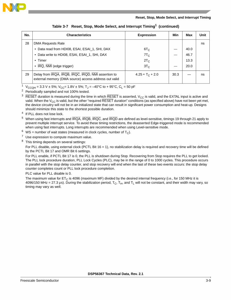
28 DMA Requests Rate
• Data read from HDI08, ESAI, ESAI_1, SHI, DAX
• Data write to HDI08, ESAI, ESAI_1, SHI, DAX
• Timer
• IRQ, NMI (edge trigger)
6TC
7TC
2TC
3TC
—
—
—
40.0
46.7
13.3
20.0
ns
29 Delay from IRQA, IRQB, IRQC, IRQD, NMI assertion to external memory (DMA source) access address out valid
4.25 × TC + 2.0 30.3 — ns
1 VCCQH = 3.3 V ± 5%; VCC= 1.8V ± 5%; TJ = –40°C to + 95°C, CL = 50 pF2 Periodically sampled and not 100% tested.3 RESET duration is measured during the time in which RESET is asserted, VCC is valid, and the EXTAL input is active and
valid. When the VCC is valid, but the other “required RESET duration” conditions (as specified above) have not been yet met, the device circuitry will not be in an initialized state that can result in significant power consumption and heat-up. Designs should minimize this state to the shortest possible duration.
4 If PLL does not lose lock.5 When using fast interrupts and IRQA, IRQB, IRQC, and IRQD are defined as level-sensitive, timings 19 through 21 apply to
prevent multiple interrupt service. To avoid these timing restrictions, the deasserted Edge-triggered mode is recommended when using fast interrupts. Long interrupts are recommended when using Level-sensitive mode.
6 WS = number of wait states (measured in clock cycles, number of TC). 7 Use expression to compute maximum value.8 This timing depends on several settings:
For PLL disable, using external clock (PCTL Bit 16 = 1), no stabilization delay is required and recovery time will be defined by the PCTL Bit 17 and OMR Bit 6 settings.For PLL enable, if PCTL Bit 17 is 0, the PLL is shutdown during Stop. Recovering from Stop requires the PLL to get locked. The PLL lock procedure duration, PLL Lock Cycles (PLC), may be in the range of 0 to 1000 cycles. This procedure occurs in parallel with the stop delay counter, and stop recovery will end when the last of these two events occurs: the stop delay counter completes count or PLL lock procedure completion.PLC value for PLL disable is 0.The maximum value for ETC is 4096 (maximum MF) divided by the desired internal frequency (i.e., for 150 MHz it is 4096/150 MHz = 27.3 µs). During the stabilization period, TC, TH, and TL will not be constant, and their width may vary, so timing may vary as well.
Table 3-7 Reset, Stop, Mode Select, and Interrupt Timing1 (continued)
No. Characteristics Expression Min Max Unit

Reset, Stop, Mode Select, and Interrupt Timing
DSP56367 Technical Data, Rev. 2.1
3-10 Freescale Semiconductor
Figure 3-2 Reset Timing
Figure 3-3 External Fast Interrupt Timing
VIH
RESET
Reset Value
First Fetch
All Pins
A0–A17
8
9 10
AA0460
A0–A17
RD
a) First Interrupt Instruction Execution
GeneralPurpose
I/O
IRQA, IRQB,IRQC, IRQD,
NMI
b) General Purpose I/O
IRQA, IRQB,IRQC, IRQD,
NMI
WR
20
21
1917
18
First Interrupt InstructionExecution/Fetch

Reset, Stop, Mode Select, and Interrupt Timing
DSP56367 Technical Data, Rev. 2.1
Freescale Semiconductor 3-11
Figure 3-4 External Interrupt Timing (Negative Edge-Triggered)
Figure 3-5 Operating Mode Select Timing
Figure 3-6 Recovery from Stop State Using IRQA Interrupt Service
IRQA, IRQB,IRQC, IRQD,
NMI
IRQA, IRQB,IRQC, IRQD,
NMI
15
16AA0463
RESET
MODA, MODB,MODC, MODD,
PINIT
VIH
IRQA, IRQB, IRQD, NMI
VIH
VIL
VIH
VIL
13
14
AA0465
First Instruction Fetch
IRQA
A0–A17
24
25
AA0466

External Memory Expansion Port (Port A)
DSP56367 Technical Data, Rev. 2.1
3-12 Freescale Semiconductor
Figure 3-7 Recovery from Stop State Using IRQA Interrupt Service
Figure 3-8 External Memory Access (DMA Source) Timing
3.10 External Memory Expansion Port (Port A)
3.10.1 SRAM TimingTable 3-8 SRAM Read and Write Accesses
No. Characteristics Symbol Expression1150 MHz
Unit Min Max
100 Address valid and AA assertion pulse width tRC, tWC (WS + 2) × TC � 4.0 [2 � WS � 7]
(WS + 3) × TC � 4.0 [WS � 8]
22.7
69.3
—
—
ns
ns
101 Address and AA valid to WR assertion tAS 0.75 × TC � 2.0[2 � WS � 3]
1.25 × TC � 2.0[WS � 4]
3.0
6.3
—
—
ns
ns
102 WR assertion pulse width tWP WS × TC � 4.0 [2 � WS � 3]
(WS � 0.5) × TC � 4.0[WS � 4]
9.3
19.3
—
—
ns
ns
103 WR deassertion to address not valid tWR 1.25 × TC � 4.0[2 � WS � 7]
2.25 × TC � 4.0[WS � 8]
4.3
11.0
—
—
ns
ns
IRQA
A0–A17 First IRQA Interrupt Instruction Fetch
26
25
AA0467
29
DMA Source Address
First Interrupt Instruction Execution
A0–A17
RD
WR
IRQA, IRQB, IRQC, IRQD,
NMI AA1104

External Memory Expansion Port (Port A)
DSP56367 Technical Data, Rev. 2.1
Freescale Semiconductor 3-13
104 Address and AA valid to input data valid tAA, tAC (WS + 0.75) × TC � 5.0 [WS � 2] — 13.3 ns
105 RD assertion to input data valid tOE (WS + 0.25) × TC � 5.0 [WS � 2] — 10.0 ns
106 RD deassertion to data not valid (data hold time) tOHZ 0.0 — ns
107 Address valid to WR deassertion2 tAW (WS + 0.75) × TC � 4.0 [WS � 2] 14.3 — ns
108 Data valid to WR deassertion (data setup time) tDS (tDW) (WS � 0.25) × TC � 3.0 [WS � 2] 8.7 — ns
109 Data hold time from WR deassertion tDH 1.25 × TC � 2.0[2 � WS � 7]
2.25 × TC � 2.0 [WS � 8]
6.3
13.0
—
—
ns
ns
110 WR assertion to data active — 0.25 × TC � 3.7 [2 � WS � 3]
�0.25 × TC � 3.7 [WS � 4]
-2.0
-5.4
—
—
ns
ns
111 WR deassertion to data high impedance — 0.25 × TC + 0.2 [2 � WS � 3]
1.25 × TC + 0.2 [4 � WS � 7]
2.25 × TC + 0.2 [WS � 8]
—
—
—
1.9
8.5
15.2
ns
ns
ns
112 Previous RD deassertion to data active (write) — 1.25 × TC � 4.0 [2 � WS � 3]
2.25 × TC � 4.0 [4 � WS � 7]
3.25 × TC � 4.0 [WS � 8]
4.3
11.0
17.7
—
—
—
ns
ns
ns
113 RD deassertion time 1.75 × TC � 4.0 [2 � WS � 7]
2.75 × TC � 4.0 [WS � 8]
7.7
14.3
—
—
ns
ns
114 WR deassertion time 2.0 × TC � 4.0 [2 � WS � 3]
2.5 × TC � 4.0 [4 � WS � 7]
3.5 × TC � 4.0 [WS � 8]
9.3
12.7
19.3
—
—
—
ns
ns
ns
115 Address valid to RD assertion 0.5 × TC � 2.0 1.3 — ns
116 RD assertion pulse width (WS + 0.25) × TC �4.0 11.0 — ns
117 RD deassertion to address not valid 1.25 × TC � 2.0 [2 � WS � 7]
2.25 × TC � 2.0 [WS � 8]
6.3
13.0
—
—
ns
ns
118 TA setup before RD or WR deassertion3 0.25 × TC + 2.0 3.7 — ns
119 TA hold after RD or WR deassertion 0.0 — ns
1 WS is the number of wait states specified in the BCR. The value is given for the minimum for a given category. (For example, for a category of [2 � WS � 7] timing is specified for 2 wait states.) Two wait states is the minimum otherwise.
2 Timings 100, 107 are guaranteed by design, not tested.3 In the case of TA negation: timing 118 is relative to the deassertion edge of RD or WR were TA to remain active.
Table 3-8 SRAM Read and Write Accesses (continued)
No. Characteristics Symbol Expression1150 MHz
Unit Min Max

External Memory Expansion Port (Port A)
DSP56367 Technical Data, Rev. 2.1
3-14 Freescale Semiconductor
Figure 3-9 SRAM Read Access
Figure 3-10 SRAM Write Access
A0–A17
RD
WR
D0–D23
AA0–AA2
115 105 106
113
104
116 117
100
AA0468
TA
119
DataIn
118
A0–A17
WR
RD
DataOutD0–D23
AA0–AA2
100
102101
107
114
108
109
103
TA
119 118

External Memory Expansion Port (Port A)
DSP56367 Technical Data, Rev. 2.1
Freescale Semiconductor 3-15
3.10.2 DRAM TimingThe selection guides provided in Figure 3-11 and Figure 3-14 should be used for primary selection only. Final selection should be based on the timing provided in the following tables. As an example, the selection guide suggests that 4 wait states must be used for 100 MHz operation when using Page Mode DRAM. However, by using the information in the appropriate table, a designer may choose to evaluate whether fewer wait states might be used by determining which timing prevents operation at 100 MHz, running the chip at a slightly lower frequency (e.g., 95 MHz), using faster DRAM (if it becomes available), and control factors such as capacitive and resistive load to improve overall system performance.
Figure 3-11 DRAM Page Mode Wait States Selection Guide
Chip Frequency(MHz)
DRAM Type(tRAC ns)
100
80
70
60
40 66 80 100
1 Wait States
2 Wait States
3 Wait States
4 Wait States
Note: This figure should be use for primary selection. For exact and detailed timings see the following tables.
AA0472
50120

External Memory Expansion Port (Port A)
DSP56367 Technical Data, Rev. 2.1
3-16 Freescale Semiconductor
Table 3-9 DRAM Page Mode Timings, Three Wait States1, 2, 3
No. Characteristics Symbol Expression4100 MHz
Unit Min Max
131 Page mode cycle time for two consecutive accesses of the same direction
Page mode cycle time for mixed (read and write) accesses
tPC 2 × TC
1.25 × TC
20.0
12.5
—
—
ns
132 CAS assertion to data valid (read) tCAC 2 × TC � 7.0 — 13.0 ns
133 Column address valid to data valid (read) tAA 3 × TC � 7.0 — 23.0 ns
134 CAS deassertion to data not valid (read hold time) tOFF 0.0 — ns
135 Last CAS assertion to RAS deassertion tRSH 2.5 × TC � 4.0 21.0 — ns
136 Previous CAS deassertion to RAS deassertion tRHCP 4.5 × TC � 4.0 41.0 — ns
137 CAS assertion pulse width tCAS 2 × TC � 4.0 16.0 — ns
138 Last CAS deassertion to RAS assertion5
• BRW[1:0] = 00, 01— not applicable
• BRW[1:0] = 10
• BRW[1:0] = 11
tCRP
4.75 × TC � 6.0
6.75 × TC � 6.0
41.5
61.5
—
—
ns
139 CAS deassertion pulse width tCP 1.5 × TC � 4.0 11.0 — ns
140 Column address valid to CAS assertion tASC TC � 4.0 6.0 — ns
141 CAS assertion to column address not valid tCAH 2.5 × TC � 4.0 21.0 — ns
142 Last column address valid to RAS deassertion tRAL 4 × TC � 4.0 36.0 — ns
143 WR deassertion to CAS assertion tRCS 1.25 × TC � 4.0 8.5 — ns
144 CAS deassertion to WR assertion tRCH 0.75 × TC � 4.0 3.5 — ns
145 CAS assertion to WR deassertion tWCH 2.25 × TC � 4.2 18.3 — ns
146 WR assertion pulse width tWP 3.5 × TC � 4.5 30.5 — ns
147 Last WR assertion to RAS deassertion tRWL 3.75 × TC � 4.3 33.2 — ns
148 WR assertion to CAS deassertion tCWL 3.25 × TC � 4.3 28.2 — ns
149 Data valid to CAS assertion (write) tDS 0.5 × TC � 4.0 1.0 — ns
150 CAS assertion to data not valid (write) tDH 2.5 × TC � 4.0 21.0 — ns
151 WR assertion to CAS assertion tWCS 1.25 × TC � 4.3 8.2 — ns
152 Last RD assertion to RAS deassertion tROH 3.5 × TC � 4.0 31.0 — ns
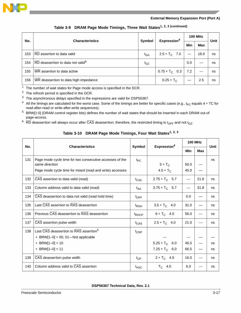
External Memory Expansion Port (Port A)
DSP56367 Technical Data, Rev. 2.1
Freescale Semiconductor 3-17
153 RD assertion to data valid tGA 2.5 × TC � 7.0 — 18.0 ns
154 RD deassertion to data not valid6 tGZ 0.0 — ns
155 WR assertion to data active 0.75 × TC � 0.3 7.2 — ns
156 WR deassertion to data high impedance 0.25 × TC — 2.5 ns
1 The number of wait states for Page mode access is specified in the DCR.2 The refresh period is specified in the DCR.3 The asynchronous delays specified in the expressions are valid for DSP56367.4 All the timings are calculated for the worst case. Some of the timings are better for specific cases (e.g., tPC equals 4 × TC for
read-after-read or write-after-write sequences).5 BRW[1:0] (DRAM control register bits) defines the number of wait states that should be inserted in each DRAM out-of
page-access.6 RD deassertion will always occur after CAS deassertion; therefore, the restricted timing is tOFF and not tGZ.
Table 3-10 DRAM Page Mode Timings, Four Wait States1, 2, 3
No. Characteristics Symbol Expression4100 MHz
Unit Min Max
131 Page mode cycle time for two consecutive accesses of the same direction
Page mode cycle time for mixed (read and write) accesses
tPC 5 × TC
4.5 × TC
50.0
45.0
—
—
ns
132 CAS assertion to data valid (read) tCAC 2.75 × TC � 5.7 — 21.8 ns
133 Column address valid to data valid (read) tAA 3.75 × TC � 5.7 — 31.8 ns
134 CAS deassertion to data not valid (read hold time) tOFF 0.0 — ns
135 Last CAS assertion to RAS deassertion tRSH 3.5 × TC � 4.0 31.0 — ns
136 Previous CAS deassertion to RAS deassertion tRHCP 6 × TC � 4.0 56.0 — ns
137 CAS assertion pulse width tCAS 2.5 × TC � 4.0 21.0 — ns
138 Last CAS deassertion to RAS assertion5
• BRW[1–0] = 00, 01—Not applicable
• BRW[1–0] = 10
• BRW[1–0] = 11
tCRP
—
5.25 × TC � 6.0
7.25 × TC � 6.0
—
46.5
66.5
—
—
—
—
ns
ns
139 CAS deassertion pulse width tCP 2 × TC � 4.0 16.0 — ns
140 Column address valid to CAS assertion tASC TC � 4.0 6.0 — ns
Table 3-9 DRAM Page Mode Timings, Three Wait States1, 2, 3 (continued)
No. Characteristics Symbol Expression4100 MHz
Unit Min Max

External Memory Expansion Port (Port A)
DSP56367 Technical Data, Rev. 2.1
3-18 Freescale Semiconductor
141 CAS assertion to column address not valid tCAH 3.5 × TC � 4.0 31.0 — ns
142 Last column address valid to RAS deassertion tRAL 5 × TC � 4.0 46.0 — ns
143 WR deassertion to CAS assertion tRCS 1.25 × TC � 4.0 8.5 — ns
144 CAS deassertion to WR assertion tRCH 1.25 × TC – 3.7 8.8 — ns
145 CAS assertion to WR deassertion tWCH 3.25 × TC � 4.2 28.3 — ns
146 WR assertion pulse width tWP 4.5 × TC � 4.5 40.5 — ns
147 Last WR assertion to RAS deassertion tRWL 4.75 × TC � 4.3 43.2 — ns
148 WR assertion to CAS deassertion tCWL 3.75 × TC � 4.3 33.2 — ns
149 Data valid to CAS assertion (write) tDS 0.5 × TC – 4.5 0.5 — ns
150 CAS assertion to data not valid (write) tDH 3.5 × TC � 4.0 31.0 — ns
151 WR assertion to CAS assertion tWCS 1.25 × TC � 4.3 8.2 — ns
152 Last RD assertion to RAS deassertion tROH 4.5 × TC � 4.0 41.0 — ns
153 RD assertion to data valid tGA 3.25 × TC � 5.7 — 26.8 ns
154 RD deassertion to data not valid6 tGZ 0.0 — ns
155 WR assertion to data active 0.75 × TC – 1.5 6.0 — ns
156 WR deassertion to data high impedance 0.25 × TC — 2.5 ns
1 The number of wait states for Page mode access is specified in the DCR.2 The refresh period is specified in the DCR.3 The asynchronous delays specified in the expressions are valid for DSP56367.4 All the timings are calculated for the worst case. Some of the timings are better for specific cases (for example, tPC equals
3 × TC for read-after-read or write-after-write sequences). An expressions is used to calculate the maximum or minimum value listed, as appropriate.
5 BRW[1–0] (DRAM control register bits) defines the number of wait states that should be inserted in each DRAM out-of-page access.
6 RD deassertion always occurs after CAS deassertion; therefore, the restricted timing is tOFF and not tGZ.
Table 3-10 DRAM Page Mode Timings, Four Wait States1, 2, 3 (continued)
No. Characteristics Symbol Expression4100 MHz
Unit Min Max

External Memory Expansion Port (Port A)
DSP56367 Technical Data, Rev. 2.1
Freescale Semiconductor 3-19
Figure 3-12 DRAM Page Mode Write Accesses
RAS
CAS
A0–A17
WR
RD
D0–D23
ColumnRow
Data Out Data Out Data Out
Last ColumnColumnAdd Address Address Address
136
135131
139
141
137140
142
147
144151
148146
155 156
150
138
145143
149
AA0473

External Memory Expansion Port (Port A)
DSP56367 Technical Data, Rev. 2.1
3-20 Freescale Semiconductor
Figure 3-13 DRAM Page Mode Read Accesses
RAS
CAS
A0–A17
WR
RD
D0–D23
Column Last ColumnColumnRow
Data In Data InData In
Add Address Address Address
136
135131
137
140141 142
143
152133
153
132
138139
134
154
AA0474

External Memory Expansion Port (Port A)
DSP56367 Technical Data, Rev. 2.1
Freescale Semiconductor 3-21
Figure 3-14 DRAM Out-of-Page Wait States Selection Guide
Table 3-11 DRAM Out-of-Page and Refresh Timings, Four Wait States1, 2
No. Characteristics Symbol Expression20 MHz3 30 MHz3
UnitMin Max Min Max
157 Random read or write cycle time tRC 5 × TC 250.0 — 166.7 — ns
158 RAS assertion to data valid (read) tRAC 2.75 × TC � 7.5 — 130.0 — 84.2 ns
159 CAS assertion to data valid (read) tCAC 1.25 × TC � 7.5 — 55.0 — 34.2 ns
160 Column address valid to data valid (read) tAA 1.5 × TC � 7.5 — 67.5 — 42.5 ns
161 CAS deassertion to data not valid (read hold time)
tOFF 0.0 — 0.0 — ns
162 RAS deassertion to RAS assertion tRP 1.75 × TC � 4.0 83.5 — 54.3 — ns
163 RAS assertion pulse width tRAS 3.25 × TC � 4.0 158.5 — 104.3 — ns
164 CAS assertion to RAS deassertion tRSH 1.75 × TC � 4.0 83.5 — 54.3 — ns
Chip Frequency(MHz)
DRAM Type(tRAC ns)
100
80
70
5066 80 100
4 Wait States
8 Wait States
11 Wait States
15 Wait States
Note: This figure should be use for primary selection. For exact and detailed timings see the following tables.
60
40
AA0475
120

External Memory Expansion Port (Port A)
DSP56367 Technical Data, Rev. 2.1
3-22 Freescale Semiconductor
165 RAS assertion to CAS deassertion tCSH 2.75 × TC � 4.0 133.5 — 87.7 — ns
166 CAS assertion pulse width tCAS 1.25 × TC � 4.0 58.5 — 37.7 — ns
167 RAS assertion to CAS assertion tRCD 1.5 × TC – 2 73.0 77.0 48.0 52.0 ns
168 RAS assertion to column address valid tRAD 1.25 × TC – 2 60.5 64.5 39.7 43.7 ns
169 CAS deassertion to RAS assertion tCRP 2.25 × TC � 4.0 108.5 — 71.0 — ns
170 CAS deassertion pulse width tCP 1.75 × TC � 4.0 83.5 — 54.3 — ns
171 Row address valid to RAS assertion tASR 1.75 × TC � 4.0 83.5 — 54.3 — ns
172 RAS assertion to row address not valid tRAH 1.25 × TC � 4.0 58.5 — 37.7 — ns
173 Column address valid to CAS assertion tASC 0.25 × TC � 4.0 8.5 — 4.3 — ns
174 CAS assertion to column address not valid tCAH 1.75 × TC � 4.0 83.5 — 54.3 — ns
175 RAS assertion to column address not valid tAR 3.25 × TC � 4.0 158.5 — 104.3 — ns
176 Column address valid to RAS deassertion tRAL 2 × TC � 4.0 96.0 — 62.7 — ns
177 WR deassertion to CAS assertion tRCS 1.5 × TC � 3.8 71.2 — 46.2 — ns
178 CAS deassertion to WR assertion tRCH 0.75 × TC � 3.7 33.8 — 21.3 — ns
179 RAS deassertion to WR assertion tRRH 0.25 × TC � 3.7 8.8 — 4.6 — ns
180 CAS assertion to WR deassertion tWCH 1.5 × TC � 4.2 70.8 — 45.8 — ns
181 RAS assertion to WR deassertion tWCR 3 × TC � 4.2 145.8 — 95.8 — ns
182 WR assertion pulse width tWP 4.5 × TC � 4.5 220.5 — 145.5 — ns
183 WR assertion to RAS deassertion tRWL 4.75 × TC � 4.3 233.2 — 154.0 — ns
184 WR assertion to CAS deassertion tCWL 4.25 × TC � 4.3 208.2 — 137.4 — ns
185 Data valid to CAS assertion (write) tDS 2.25 × TC � 4.0 108.5 — 71.0 — ns
186 CAS assertion to data not valid (write) tDH 1.75 × TC � 4.0 83.5 — 54.3 — ns
187 RAS assertion to data not valid (write) tDHR 3.25 × TC � 4.0 158.5 — 104.3 — ns
188 WR assertion to CAS assertion tWCS 3 × TC � 4.3 145.7 — 95.7 — ns
189 CAS assertion to RAS assertion (refresh) tCSR 0.5 × TC � 4.0 21.0 — 12.7 — ns
190 RAS deassertion to CAS assertion (refresh) tRPC 1.25 × TC � 4.0 58.5 — 37.7 — ns
Table 3-11 DRAM Out-of-Page and Refresh Timings, Four Wait States1, 2 (continued)
No. Characteristics Symbol Expression20 MHz3 30 MHz3
UnitMin Max Min Max

External Memory Expansion Port (Port A)
DSP56367 Technical Data, Rev. 2.1
Freescale Semiconductor 3-23
191 RD assertion to RAS deassertion tROH 4.5 × TC � 4.0 221.0 — 146.0 — ns
192 RD assertion to data valid tGA 4 × TC � 7.5 — 192.5 — 125.8 ns
193 RD deassertion to data not valid4 tGZ 0.0 — 0.0 — ns
194 WR assertion to data active 0.75 × TC � 0.3 37.2 — 24.7 — ns
195 WR deassertion to data high impedance 0.25 × TC — 12.5 — 8.3 ns
1 The number of wait states for out of page access is specified in the DCR.2 The refresh period is specified in the DCR.3 Reduced DSP clock speed allows use of DRAM out-of-page access with four Wait states (Figure 3-14).4 RD deassertion will always occur after CAS deassertion; therefore, the restricted timing is tOFF and not tGZ.
Table 3-12 DRAM Out-of-Page and Refresh Timings, Eleven Wait States1, 2, 3
No. Characteristics Symbol Expression100 MHz
Unit Min Max
157 Random read or write cycle time tRC 12 × TC 120.0 — ns
158 RAS assertion to data valid (read) tRAC 6.25 × TC � 7.0 — 55.5 ns
159 CAS assertion to data valid (read) tCAC 3.75 × TC � 7.0 — 30.5 ns
160 Column address valid to data valid (read) tAA 4.5 × TC � 7.0 — 38.0 ns
161 CAS deassertion to data not valid (read hold time) tOFF 0.0 — ns
162 RAS deassertion to RAS assertion tRP 4.25 × TC � 4.0 38.5 — ns
163 RAS assertion pulse width tRAS 7.75 × TC � 4.0 73.5 — ns
164 CAS assertion to RAS deassertion tRSH 5.25 × TC � 4.0 48.5 — ns
165 RAS assertion to CAS deassertion tCSH 6.25 × TC � 4.0 58.5 — ns
166 CAS assertion pulse width tCAS 3.75 × TC � 4.0 33.5 — ns
167 RAS assertion to CAS assertion tRCD 2.5 × TC – 4.0 21.0 29.0 ns
168 RAS assertion to column address valid tRAD 1.75 × TC – 4.0 13.5 21.5 ns
169 CAS deassertion to RAS assertion tCRP 5.75 × TC � 4.0 53.5 — ns
170 CAS deassertion pulse width tCP 4.25 × TC � 4.0 38.5 — ns
171 Row address valid to RAS assertion tASR 4.25 × TC � 4.0 38.5 — ns
172 RAS assertion to row address not valid tRAH 1.75 × TC � 4.0 13.5 — ns
Table 3-11 DRAM Out-of-Page and Refresh Timings, Four Wait States1, 2 (continued)
No. Characteristics Symbol Expression20 MHz3 30 MHz3
UnitMin Max Min Max

External Memory Expansion Port (Port A)
DSP56367 Technical Data, Rev. 2.1
3-24 Freescale Semiconductor
173 Column address valid to CAS assertion tASC 0.75 × TC � 4.0 3.5 — ns
174 CAS assertion to column address not valid tCAH 5.25 × TC � 4.0 48.5 — ns
175 RAS assertion to column address not valid tAR 7.75 × TC � 4.0 73.5 — ns
176 Column address valid to RAS deassertion tRAL 6 × TC � 4.0 56.0 — ns
177 WR deassertion to CAS assertion tRCS 3.0 × TC � 4.0 26.0 — ns
178 CAS deassertion to WR4 assertion tRCH 1.75 × TC � 4.0 13.5 — ns
179 RAS deassertion to WR4 assertion tRRH 0.25 × TC � 2.0 0.5 — ns
180 CAS assertion to WR deassertion tWCH 5 × TC � 4.2 45.8 — ns
181 RAS assertion to WR deassertion tWCR 7.5 × TC � 4.2 70.8 — ns
182 WR assertion pulse width tWP 11.5 × TC � 4.5 110.5 — ns
183 WR assertion to RAS deassertion tRWL 11.75 × TC � 4.3 113.2 — ns
184 WR assertion to CAS deassertion tCWL 10.25 × TC � 4.3 103.2 — ns
185 Data valid to CAS assertion (write) tDS 5.75 × TC � 4.0 53.5 — ns
186 CAS assertion to data not valid (write) tDH 5.25 × TC � 4.0 48.5 — ns
187 RAS assertion to data not valid (write) tDHR 7.75 × TC � 4.0 73.5 — ns
188 WR assertion to CAS assertion tWCS 6.5 × TC � 4.3 60.7 — ns
189 CAS assertion to RAS assertion (refresh) tCSR 1.5 × TC � 4.0 11.0 — ns
190 RAS deassertion to CAS assertion (refresh) tRPC 2.75 × TC � 4.0 23.5 — ns
191 RD assertion to RAS deassertion tROH 11.5 × TC � 4.0 111.0 — ns
192 RD assertion to data valid tGA 10 × TC � 7.0 — 93.0 ns
193 RD deassertion to data not valid5 tGZ 0.0 — ns
194 WR assertion to data active 0.75 × TC � 0.3 7.2 — ns
195 WR deassertion to data high impedance 0.25 × TC — 2.5 ns
1 The number of wait states for out-of-page access is specified in the DCR.2 The refresh period is specified in the DCR.3 The asynchronous delays specified in the expressions are valid for DSP56367.4 Either tRCH or tRRH must be satisfied for read cycles.5 RD deassertion will always occur after CAS deassertion; therefore, the restricted timing is tOFF and not tGZ.
Table 3-12 DRAM Out-of-Page and Refresh Timings, Eleven Wait States1, 2, 3 (continued)
No. Characteristics Symbol Expression100 MHz
Unit Min Max

External Memory Expansion Port (Port A)
DSP56367 Technical Data, Rev. 2.1
Freescale Semiconductor 3-25
Table 3-13 DRAM Out-of-Page and Refresh Timings, Fifteen Wait States1, 2
No. Characteristics Symbol Expression3100 MHz
Unit Min Max
157 Random read or write cycle time tRC 16 × TC 160.0 — ns
158 RAS assertion to data valid (read) tRAC 8.25 × TC � 5.7 — 76.8 ns
159 CAS assertion to data valid (read) tCAC 4.75 × TC � 5.7 — 41.8 ns
160 Column address valid to data valid (read) tAA 5.5 × TC � 5.7 — 49.3 ns
161 CAS deassertion to data not valid (read hold time) tOFF 0.0 0.0 — ns
162 RAS deassertion to RAS assertion tRP 6.25 × TC � 4.0 58.5 — ns
163 RAS assertion pulse width tRAS 9.75 × TC � 4.0 93.5 — ns
164 CAS assertion to RAS deassertion tRSH 6.25 × TC � 4.0 58.5 — ns
165 RAS assertion to CAS deassertion tCSH 8.25 × TC � 4.0 78.5 — ns
166 CAS assertion pulse width tCAS 4.75 × TC � 4.0 43.5 — ns
167 RAS assertion to CAS assertion tRCD 3.5 × TC – 2 33.0 37.0 ns
168 RAS assertion to column address valid tRAD 2.75 × TC – 2 25.5 29.5 ns
169 CAS deassertion to RAS assertion tCRP 7.75 × TC � 4.0 73.5 — ns
170 CAS deassertion pulse width tCP 6.25 × TC – 6.0 56.5 — ns
171 Row address valid to RAS assertion tASR 6.25 × TC � 4.0 58.5 — ns
172 RAS assertion to row address not valid tRAH 2.75 × TC � 4.0 23.5 — ns
173 Column address valid to CAS assertion tASC 0.75 × TC � 4.0 3.5 — ns
174 CAS assertion to column address not valid tCAH 6.25 × TC � 4.0 58.5 — ns
175 RAS assertion to column address not valid tAR 9.75 × TC � 4.0 93.5 — ns
176 Column address valid to RAS deassertion tRAL 7 × TC � 4.0 66.0 — ns
177 WR deassertion to CAS assertion tRCS 5 × TC � 3.8 46.2 — ns
178 CAS deassertion to WR4 assertion tRCH 1.75 × TC – 3.7 13.8 — ns
179 RAS deassertion to WR4 assertion tRRH 0.25 × TC � 2.0 0.5 — ns
180 CAS assertion to WR deassertion tWCH 6 × TC � 4.2 55.8 — ns
181 RAS assertion to WR deassertion tWCR 9.5 × TC � 4.2 90.8 — ns
182 WR assertion pulse width tWP 15.5 × TC � 4.5 150.5 — ns

External Memory Expansion Port (Port A)
DSP56367 Technical Data, Rev. 2.1
3-26 Freescale Semiconductor
183 WR assertion to RAS deassertion tRWL 15.75 × TC � 4.3 153.2 — ns
184 WR assertion to CAS deassertion tCWL 14.25 × TC � 4.3 138.2 — ns
185 Data valid to CAS assertion (write) tDS 8.75 × TC � 4.0 83.5 — ns
186 CAS assertion to data not valid (write) tDH 6.25 × TC � 4.0 58.5 — ns
187 RAS assertion to data not valid (write) tDHR 9.75 × TC � 4.0 93.5 — ns
188 WR assertion to CAS assertion tWCS 9.5 × TC � 4.3 90.7 — ns
189 CAS assertion to RAS assertion (refresh) tCSR 1.5 × TC � 4.0 11.0 — ns
190 RAS deassertion to CAS assertion (refresh) tRPC 4.75 × TC � 4.0 43.5 — ns
191 RD assertion to RAS deassertion tROH 15.5 × TC � 4.0 151.0 — ns
192 RD assertion to data valid tGA 14 × TC � 5.7 — 134.3 ns
193 RD deassertion to data not valid5 tGZ 0.0 — ns
194 WR assertion to data active 0.75 × TC – 1.5 6.0 — ns
195 WR deassertion to data high impedance 0.25 × TC — 2.5 ns
1 The number of wait states for an out-of-page access is specified in the DCR.2 The refresh period is specified in the DCR.3 An expression is used to compute the maximum or minimum value listed (or both if the expression includes ±). 4 Either tRCH or tRRH must be satisfied for read cycles.5 RD deassertion always occurs after CAS deassertion; therefore, the restricted timing is tOFF and not tGZ.
Table 3-13 DRAM Out-of-Page and Refresh Timings, Fifteen Wait States1, 2 (continued)
No. Characteristics Symbol Expression3100 MHz
Unit Min Max

External Memory Expansion Port (Port A)
DSP56367 Technical Data, Rev. 2.1
Freescale Semiconductor 3-27
Figure 3-15 DRAM Out-of-Page Read Access
RAS
CAS
A0–A17
WR
RD
D0–D23Data
Row Address Column Address
In
157
163
165
162162
169
170
171
168
167164
166
173174
175
172177
176
191
160 168
159
193
161192
158
179
AA0476

External Memory Expansion Port (Port A)
DSP56367 Technical Data, Rev. 2.1
3-28 Freescale Semiconductor
Figure 3-16 DRAM Out-of-Page Write Access
RAS
CAS
A0–A17
WR
RD
D0–D23 Data Out
Column AddressRow Address
162 163
165
162
157
169
170
167
168
164
166
171 173
174
176
172
181
175
180188
182
184
183
187
185
194
186
195
AA0477

External Memory Expansion Port (Port A)
DSP56367 Technical Data, Rev. 2.1
Freescale Semiconductor 3-29
Figure 3-17 DRAM Refresh Access
3.10.3 Arbitration TimingsTable 3-14 Asynchronous Bus Arbitration Timing1, 2, 3
1 Bit 13 in the OMR register must be set to enter Asynchronous Arbitration mode.2 If Asynchronous Arbitration mode is active, none of the timings in Table 3-14 is required.3 In order to guarantee timings 250, and 251, it is recommended to assert BG inputs to different 56300 devices (on the same
bus) in a non overlap manner as shown in Figure 3-18.
No. Characteristics Expression150 MHz
Unit Min Max
250 BB assertion window from BG input negation. 2 .5* Tc + 5 — 21.7 ns
251 Delay from BB assertion to BG assertion 2 * Tc + 5 18.3 — ns
RAS
CAS
WR
157
163 162162
190
170 165
189
177
AA0478

External Memory Expansion Port (Port A)
DSP56367 Technical Data, Rev. 2.1
3-30 Freescale Semiconductor
Figure 3-18 Asynchronous Bus Arbitration Timing
Figure 3-19 Asynchronous Bus Arbitration Timing
3.10.4 Background explanation for Asynchronous Bus Arbitration:The asynchronous bus arbitration is enabled by internal synchronization circuits on BG and BB inputs. These synchronization circuits add delay from the external signal until it is exposed to internal logic. As a result of this delay, a 56300 part may assume mastership and assert BB for some time after BG is negated. This is the reason for timing 250.
Once BB is asserted, there is a synchronization delay from BB assertion to the time this assertion is exposed to other 56300 components which are potential masters on the same bus. If BG input is asserted before that time, a situation of BG asserted, and BB negated, may cause another 56300 component to assume mastership at the same time. Therefore some non-overlap period between one BG input active to another BG input active is required. Timing 251 ensures that such a situation is avoided.
BG1
BB
250
251BG2
BG1
BG2
250+251

Parallel Host Interface (HDI08) Timing
DSP56367 Technical Data, Rev. 2.1
Freescale Semiconductor 3-31
3.11 Parallel Host Interface (HDI08) TimingTable 3-15 Host Interface (HDI08) Timing1, 2, 3
No. Characteristics Expression150 MHz
UnitMin Max
317 Read data strobe assertion width4
HACK read assertion width
TC + 9.9 16.7 — ns
318 Read data strobe deassertion width4
HACK read deassertion width
— 9.9 — ns
319 Read data strobe deassertion width4 after “Last Data Register” reads5, 6, or between two consecutive CVR, ICR, or ISR reads7
HACK deassertion width after “Last Data Register” reads5, 6
2.5 × TC + 6.6 23.3 — ns
320 Write data strobe assertion width8
HACK write assertion width
— 13.2 — ns
321 Write data strobe deassertion width8
HACK write deassertion width
• after ICR, CVR and “Last Data Register” writes5
• after IVR writes, or
• after TXH:TXM writes (with HBE=0), or
• after TXL:TXM writes (with HBE=1)
2.5 × TC + 6.6 23.3
16.5
—
—
ns
322 HAS assertion width — 9.9 — ns
323 HAS deassertion to data strobe assertion9 — 0.0 — ns
324 Host data input setup time before write data strobe deassertion8
Host data input setup time before HACK write deassertion
— 9.9 — ns
325 Host data input hold time after write data strobe deassertion8
Host data input hold time after HACK write deassertion
— 3.3 — ns
326 Read data strobe assertion to output data active from high impedance4
HACK read assertion to output data active from high impedance
— 3.3 — ns
327 Read data strobe assertion to output data valid4
HACK read assertion to output data valid
— — 24.2 ns
328 Read data strobe deassertion to output data high impedance4
HACK read deassertion to output data high impedance
— — 9.9 ns
329 Output data hold time after read data strobe deassertion4
Output data hold time after HACK read deassertion
— 3.3 — ns
330 HCS assertion to read data strobe deassertion4 TC +9.9 16.7 — ns
331 HCS assertion to write data strobe deassertion8 — 9.9 — ns

Parallel Host Interface (HDI08) Timing
DSP56367 Technical Data, Rev. 2.1
3-32 Freescale Semiconductor
332 HCS assertion to output data valid — — 19.1 ns
333 HCS hold time after data strobe deassertion9 — 0.0 — ns
334 Address (AD7–AD0) setup time before HAS deassertion (HMUX=1) — 4.7 — ns
335 Address (AD7–AD0) hold time after HAS deassertion (HMUX=1) — 3.3 — ns
336 A10–A8 (HMUX=1), A2–A0 (HMUX=0), HR/W setup time before data strobe assertion9
• Read
• Write
— 0
4.7
—
—
ns
337 A10–A8 (HMUX=1), A2–A0 (HMUX=0), HR/W hold time after data strobe deassertion9
— 3.3 — ns
338 Delay from read data strobe deassertion to host request assertion for “Last Data Register” read4, 5, 10
TC 6.7 — ns
339 Delay from write data strobe deassertion to host request assertion for “Last Data Register” write5, 8, 10
2 × TC 13.4 — ns
340 Delay from data strobe assertion to host request deassertion for “Last Data Register” read or write (HROD = 0)5, 9, 10
— — 19.1 ns
341 Delay from data strobe assertion to host request deassertion for “Last Data Register” read or write (HROD = 1, open drain Host Request)5, 9, 10, 11
— — 300.0 ns
342 Delay from DMA HACK deassertion to HOREQ assertion
• For “Last Data Register” read5
• For “Last Data Register” write5
• For other cases
2 × TC + 19.1
1.5 × TC + 19.1
32.5
29.2
0.0
—
—
—
ns
343 Delay from DMA HACK assertion to HOREQ deassertion
• HROD = 05— — 20.2 ns
344 Delay from DMA HACK assertion to HOREQ deassertion for “Last Data Register” read or write
• HROD = 1, open drain Host Request5, 11
— — 300.0 ns
1 See Host Port Usage Considerations in the DSP56367 User’s Manual.2 In the timing diagrams below, the controls pins are drawn as active low. The pin polarity is programmable.3 VCC = 1.8 V ± 5%; TJ = –40°C to +95°C, CL = 50 pF4 The read data strobe is HRD in the dual data strobe mode and HDS in the single data strobe mode.5 The “last data register” is the register at address $7, which is the last location to be read or written in data transfers.6 This timing is applicable only if a read from the “last data register” is followed by a read from the RXL, RXM, or RXH registers
without first polling RXDF or HREQ bits, or waiting for the assertion of the HOREQ signal.7 This timing is applicable only if two consecutive reads from one of these registers are executed.8 The write data strobe is HWR in the dual data strobe mode and HDS in the single data strobe mode.
Table 3-15 Host Interface (HDI08) Timing1, 2, 3 (continued)
No. Characteristics Expression150 MHz
UnitMin Max

Parallel Host Interface (HDI08) Timing
DSP56367 Technical Data, Rev. 2.1
Freescale Semiconductor 3-33
Figure 3-20 Host Interrupt Vector Register (IVR) Read Timing Diagram
Figure 3-21 Read Timing Diagram, Non-Multiplexed Bus
9 The data strobe is host read (HRD) or host write (HWR) in the dual data strobe mode and host data strobe (HDS) in the single data strobe mode.
10 The host request is HOREQ in the single host request mode and HRRQ and HTRQ in the double host request mode.11 In this calculation, the host request signal is pulled up by a 4.7 k� resistor in the open-drain mode.
HACK
HD7–HD0
HOREQ
329
317 318
328
326
327
AA1105
HRD, HDS
HA0–HA2
HCS
HD0–HD7
HOREQ,
327
332 319
318
317
330
329
337336
328
326
338
341
340
333
AA0484
HRRQ, HTRQ

Parallel Host Interface (HDI08) Timing
DSP56367 Technical Data, Rev. 2.1
3-34 Freescale Semiconductor
Figure 3-22 Write Timing Diagram, Non-Multiplexed Bus
HWR, HDS
HA0–HA2
HCS
HD0–HD7
HOREQ, HRRQ, HTRQ
336331
337
321
320
324325
339340
341
333
AA0485

Parallel Host Interface (HDI08) Timing
DSP56367 Technical Data, Rev. 2.1
Freescale Semiconductor 3-35
Figure 3-23 Read Timing Diagram, Multiplexed Bus
HRD, HDS
HA8–HA10
HAS
HAD0–HAD7
HOREQ, HRRQ, HTRQ
Address Data
317
318
319328
329
327
326
335
336 337
334
341
340 338
323
AA0486
322

Parallel Host Interface (HDI08) Timing
DSP56367 Technical Data, Rev. 2.1
3-36 Freescale Semiconductor
Figure 3-24 Write Timing Diagram, Multiplexed Bus
Figure 3-25 Host DMA Write Timing Diagram
HWR, HDS
HA8–HA10
HOREQ, HRRQ, HTRQ
HAS
HAD0–HAD7 Address Data
320
321
325
324
335
341
339
336
334
340
322
323
AA0487
HOREQ(Output)
HACK(Input)
H0–H7(Input)
DataValid
TXH/M/L Write
320 321
343 342
324
344
325

Serial Host Interface SPI Protocol Timing
DSP56367 Technical Data, Rev. 2.1
Freescale Semiconductor 3-37
Figure 3-26 Host DMA Read Timing Diagram
3.12 Serial Host Interface SPI Protocol TimingTable 3-16 Serial Host Interface SPI Protocol Timing
No. Characteristics1 Mode FilterMode Expression2 Min Max Unit
140 Tolerable spike width on clock or data in — Bypassed
Narrow
Wide
—
—
—
—
—
—
0
50
100
ns
141 Minimum serial clock cycle = tSPICC(min) Master Bypassed
Narrow
Wide
6 × TC+46
6 × TC+152
6 × TC+223
86.2
192.2
263.2
—
—
—
ns
142 Serial clock high period Master Bypassed
Narrow
Wide
0.5 × tSPICC –10
0.5 × tSPICC –10
0.5 × tSPICC –10
38
91
126.5
—
—
—
ns
Slave Bypassed
Narrow
Wide
2.5 × TC + 12
2.5 × TC + 102
2.5 × TC + 189
28.8
118.8
205.8
—
—
—
ns
143 Serial clock low period Master Bypassed
Narrow
Wide
0.5 × tSPICC –10
0.5 × tSPICC –10
0.5 × tSPICC –10
38 — ns
Slave Bypassed
Narrow
Wide
2.5 × TC + 12
2.5 × TC + 102
2.5 × TC + 189
28.8
118.8
205.8
—
—
—
ns
326
317 318
327 328
329
DataValid
HOREQ(Output)
HACK(Input)
H0-H7(Output)
RXH Read
343 342342

Serial Host Interface SPI Protocol Timing
DSP56367 Technical Data, Rev. 2.1
3-38 Freescale Semiconductor
144 Serial clock rise/fall time Master
Slave
—
—
—
—
—
—
10
2000
ns
146 SS assertion to first SCK edge
CPHA = 0
Slave Bypassed
Narrow
Wide
3.5 × TC + 15
0
0
38.5
0
0
—
—
—
ns
CPHA = 1 Slave Bypassed
Narrow
Wide
10
0
0
10
0
0
—
—
—
ns
147 Last SCK edge to SS not asserted Slave Bypassed
Narrow
Wide
12
102
189
12
102
189
—
—
—
ns
148 Data input valid to SCK edge (data input set-up time)
Master/Slave
Bypassed
Narrow
Wide
0
MAX{(20-TC), 0}
MAX{(40-TC), 0}
0
13.3
33.3
—
—
—
ns
149 SCK last sampling edge to data input not valid
Master/Slave
Bypassed
Narrow
Wide
2.5 × TC + 10
2.5 × TC + 30
2.5 × TC + 50
26.8
46.8
66.8
—
—
—
ns
150 SS assertion to data out active Slave — 2 2 — ns
151 SS deassertion to data high impedance3 Slave — 9 — 9 ns
152 SCK edge to data out valid (data out delay time)
Master/Slave
Bypassed
Narrow
Wide
2 × TC + 33
2 × TC + 123
2 × TC + 210
—
—
—
46.4
136.4
223.4
ns
153 SCK edge to data out not valid (data out hold time)
Master/Slave
Bypassed
Narrow
Wide
TC + 5
TC + 55
TC + 106
11.7
61.7
112.7
—
—
—
ns
154 SS assertion to data out valid (CPHA = 0) Slave — TC + 33 — 39.7 ns
157 First SCK sampling edge to HREQ output deassertion
Slave Bypassed
Narrow
Wide
2.5 × TC + 30
2.5 × TC + 120
2.5 × TC + 217
—
—
—
46.8
136.8
233.8
ns
158 Last SCK sampling edge to HREQ output not deasserted (CPHA = 1)
Slave Bypassed
Narrow
Wide
2.5 × TC + 30
2.5 × TC + 80
2.5 × TC + 136
46.8
96.8
152.8
—
—
—
ns
159 SS deassertion to HREQ output not deasserted (CPHA = 0)
Slave — 2.5 × TC + 30 46.8 — ns
Table 3-16 Serial Host Interface SPI Protocol Timing (continued)
No. Characteristics1 Mode FilterMode Expression2 Min Max Unit

Serial Host Interface SPI Protocol Timing
DSP56367 Technical Data, Rev. 2.1
Freescale Semiconductor 3-39
Figure 3-27 SPI Master Timing (CPHA = 0)
160 SS deassertion pulse width (CPHA = 0) Slave — TC + 6 12.7 — ns
161 HREQ in assertion to first SCK edge Master Bypassed
Narrow
Wide
0.5 × tSPICC + 2.5 × TC + 43
0.5 × tSPICC + 2.5 × TC + 43
0.5 × tSPICC + 2.5 × TC + 43
97.8
160.8
196.8
—
—
—
ns
162 HREQ in deassertion to last SCK sampling edge (HREQ in set-up time) (CPHA = 1)
Master — 0 0 — ns
163 First SCK edge to HREQ in not asserted
(HREQ in hold time)
Master — 0 0 — ns
1 VCC = 1.8 V ± 5%; TJ = –40°C to +95°C, CL = 50 pF2 The timing values calculated are based on simulation data at 150MHz. Tester restrictions limit SHI testing to lower clock
frequencies.3 Periodically sampled, not 100% tested
Table 3-16 Serial Host Interface SPI Protocol Timing (continued)
No. Characteristics1 Mode FilterMode Expression2 Min Max Unit
SS(Input)
SCK (CPOL = 0)(Output)
SCK (CPOL = 1)(Output)
MISO(Input) Valid
MOSI(Output)
MSBValidLSB
MSB LSB
HREQ(Input)
141142
143144 144
141
144144143
142
148149
149148
152 153
163161
AA0271

Serial Host Interface SPI Protocol Timing
DSP56367 Technical Data, Rev. 2.1
3-40 Freescale Semiconductor
Figure 3-28 SPI Master Timing (CPHA = 1)
SS(Input)
SCK (CPOL = 0)(Output)
SCK (CPOL = 1)(Output)
MISO(Input) Valid
MOSI(Output)
MSBValidLSB
MSB LSB
HREQ(Input)
141
142
143
144 144
141
144144143
142
148 148149
152 153
163161 162
149
AA0272

Serial Host Interface SPI Protocol Timing
DSP56367 Technical Data, Rev. 2.1
Freescale Semiconductor 3-41
Figure 3-29 SPI Slave Timing (CPHA = 0)
SS(Input)
SCK (CPOL = 0)(Input)
SCK (CPOL = 1)(Input)
MISO(Output)
MOSI(Input)
MSB LSB
MSB LSB
HREQ(Output)
141142
143144 144
141
144144143
142
154
150152
153
148149
159157
153 151
Valid Valid
148149
147
160
146
AA0273

Serial Host Interface (SHI) I2C Protocol Timing
DSP56367 Technical Data, Rev. 2.1
3-42 Freescale Semiconductor
Figure 3-30 SPI Slave Timing (CPHA = 1)
3.13 Serial Host Interface (SHI) I2C Protocol TimingTable 3-17 SHI I2C Protocol Timing
Standard I2C
No. Characteristics1, 2, 3 Symbol/Expression
Standard4, 5 Fast-Mode5, 6 Unit
Min Max Min Max
Tolerable spike width on SCL or SDA
• Filters bypassed
• Narrow filters enabled
• Wide filters enabled
—
—
—
—
0
50
100
—
—
—
0
50
100
ns
171 SCL clock frequency FSCL — 100 — 400 kHz
171 SCL clock cycle TSCL 10 — 2.5 — µs
172 Bus free time TBUF 4.7 — 1.3 — µs
173 Start condition set-up time TSU;STA 4.7 — 0.6 — µs
174 Start condition hold time THD;STA 4.0 — 0.6 — µs
SS(Input)
SCK (CPOL = 0)(Input)
SCK (CPOL = 1)(Input)
MISO(Output)
MOSI(Input)
MSB LSB
MSB LSB
HREQ(Output)
141
142
143
144 144
144144143
142