dsp builder advanced blockset reference manualapplication-notes.digchip.com/038/38-21454.pdf ·...
TRANSCRIPT
101 Innovation DriveSan Jose, CA 95134www.altera.com
DSP Builder Advanced BlocksetReference Manual
Software Version: 8.1Document Date: November 2008

Copyright © 2008 Altera Corporation. All rights reserved. Altera, The Programmable Solutions Company, the stylized Altera logo, specific device designations, and all otherwords and logos that are identified as trademarks and/or service marks are, unless noted otherwise, the trademarks and service marks of Altera Corporation in the U.S. and othercountries. All other product or service names are the property of their respective holders. Altera products are protected under numerous U.S. and foreign patents and pending ap-plications, maskwork rights, and copyrights. Altera warrants performance of its semiconductor products to current specifications in accordance with Altera's standard warranty,but reserves the right to make changes to any products and services at any time without notice. Altera assumes no responsibility or liability arising out of the application or use ofany information, product, or service described herein except as expressly agreed to in writing by Altera Corporation. Altera customers are advised to obtain the latest version ofdevice specifications before relying on any published information and before placing orders for products or services.
MNL-01031-2.0
© November 2008 Altera Corporation
Contents
Chapter 1. IntroductionDesign Flow . . . . . . . . . . . . . . . . . . . . . . . . . . . . . . . . . . . . . . . . . . . . . . . . . . . . . . . . . . . . . . . . . . . . . . . . . . . . 1–1Libraries . . . . . . . . . . . . . . . . . . . . . . . . . . . . . . . . . . . . . . . . . . . . . . . . . . . . . . . . . . . . . . . . . . . . . . . . . . . . . . . 1–1
Chapter 2. Base LibraryChannel Viewer (ChanView) . . . . . . . . . . . . . . . . . . . . . . . . . . . . . . . . . . . . . . . . . . . . . . . . . . . . . . . . . . . . . . 2–1Control . . . . . . . . . . . . . . . . . . . . . . . . . . . . . . . . . . . . . . . . . . . . . . . . . . . . . . . . . . . . . . . . . . . . . . . . . . . . . . . . 2–3Device . . . . . . . . . . . . . . . . . . . . . . . . . . . . . . . . . . . . . . . . . . . . . . . . . . . . . . . . . . . . . . . . . . . . . . . . . . . . . . . . . 2–4Edit Params . . . . . . . . . . . . . . . . . . . . . . . . . . . . . . . . . . . . . . . . . . . . . . . . . . . . . . . . . . . . . . . . . . . . . . . . . . . . 2–5Run ModelSim . . . . . . . . . . . . . . . . . . . . . . . . . . . . . . . . . . . . . . . . . . . . . . . . . . . . . . . . . . . . . . . . . . . . . . . . . . 2–8Run Quartus II . . . . . . . . . . . . . . . . . . . . . . . . . . . . . . . . . . . . . . . . . . . . . . . . . . . . . . . . . . . . . . . . . . . . . . . . . . 2–9Scale . . . . . . . . . . . . . . . . . . . . . . . . . . . . . . . . . . . . . . . . . . . . . . . . . . . . . . . . . . . . . . . . . . . . . . . . . . . . . . . . . . 2–10Signals . . . . . . . . . . . . . . . . . . . . . . . . . . . . . . . . . . . . . . . . . . . . . . . . . . . . . . . . . . . . . . . . . . . . . . . . . . . . . . . . 2–12
Chapter 3. Filter LibraryFIR and CIC Filters . . . . . . . . . . . . . . . . . . . . . . . . . . . . . . . . . . . . . . . . . . . . . . . . . . . . . . . . . . . . . . . . . . . . . . 3–1Single Rate FIR . . . . . . . . . . . . . . . . . . . . . . . . . . . . . . . . . . . . . . . . . . . . . . . . . . . . . . . . . . . . . . . . . . . . . . . . . . 3–4Interpolating FIR . . . . . . . . . . . . . . . . . . . . . . . . . . . . . . . . . . . . . . . . . . . . . . . . . . . . . . . . . . . . . . . . . . . . . . . . 3–7Decimating FIR . . . . . . . . . . . . . . . . . . . . . . . . . . . . . . . . . . . . . . . . . . . . . . . . . . . . . . . . . . . . . . . . . . . . . . . . 3–11Fractional Rate FIR . . . . . . . . . . . . . . . . . . . . . . . . . . . . . . . . . . . . . . . . . . . . . . . . . . . . . . . . . . . . . . . . . . . . . 3–15Interpolating CIC . . . . . . . . . . . . . . . . . . . . . . . . . . . . . . . . . . . . . . . . . . . . . . . . . . . . . . . . . . . . . . . . . . . . . . . 3–19Decimating CIC . . . . . . . . . . . . . . . . . . . . . . . . . . . . . . . . . . . . . . . . . . . . . . . . . . . . . . . . . . . . . . . . . . . . . . . . 3–23
Chapter 4. FFT LibraryComplex Multiplier (ComplexMult) . . . . . . . . . . . . . . . . . . . . . . . . . . . . . . . . . . . . . . . . . . . . . . . . . . . . . . . 4–2Complex Sample Delay . . . . . . . . . . . . . . . . . . . . . . . . . . . . . . . . . . . . . . . . . . . . . . . . . . . . . . . . . . . . . . . . . . 4–3Dual Twiddle Memory . . . . . . . . . . . . . . . . . . . . . . . . . . . . . . . . . . . . . . . . . . . . . . . . . . . . . . . . . . . . . . . . . . . 4–5Negate . . . . . . . . . . . . . . . . . . . . . . . . . . . . . . . . . . . . . . . . . . . . . . . . . . . . . . . . . . . . . . . . . . . . . . . . . . . . . . . . . 4–6Negate Parameterizable . . . . . . . . . . . . . . . . . . . . . . . . . . . . . . . . . . . . . . . . . . . . . . . . . . . . . . . . . . . . . . . . . . 4–6Butterfly I (BFI) . . . . . . . . . . . . . . . . . . . . . . . . . . . . . . . . . . . . . . . . . . . . . . . . . . . . . . . . . . . . . . . . . . . . . . . . . 4–7Butterfly II (BFII) . . . . . . . . . . . . . . . . . . . . . . . . . . . . . . . . . . . . . . . . . . . . . . . . . . . . . . . . . . . . . . . . . . . . . . . . 4–8Bit Reverse Core . . . . . . . . . . . . . . . . . . . . . . . . . . . . . . . . . . . . . . . . . . . . . . . . . . . . . . . . . . . . . . . . . . . . . . . 4–10Twiddle Generator . . . . . . . . . . . . . . . . . . . . . . . . . . . . . . . . . . . . . . . . . . . . . . . . . . . . . . . . . . . . . . . . . . . . . 4–11
Chapter 5. Waveform Synthesis LibraryComplex Mixer . . . . . . . . . . . . . . . . . . . . . . . . . . . . . . . . . . . . . . . . . . . . . . . . . . . . . . . . . . . . . . . . . . . . . . . . . 5–1Real Mixer . . . . . . . . . . . . . . . . . . . . . . . . . . . . . . . . . . . . . . . . . . . . . . . . . . . . . . . . . . . . . . . . . . . . . . . . . . . . . . 5–3NCO . . . . . . . . . . . . . . . . . . . . . . . . . . . . . . . . . . . . . . . . . . . . . . . . . . . . . . . . . . . . . . . . . . . . . . . . . . . . . . . . . . . 5–5
Chapter 6. ModelBus LibraryBus Slave . . . . . . . . . . . . . . . . . . . . . . . . . . . . . . . . . . . . . . . . . . . . . . . . . . . . . . . . . . . . . . . . . . . . . . . . . . . . . . . 6–1Bus Stimulus . . . . . . . . . . . . . . . . . . . . . . . . . . . . . . . . . . . . . . . . . . . . . . . . . . . . . . . . . . . . . . . . . . . . . . . . . . . . 6–2Bus Stimulus File Reader . . . . . . . . . . . . . . . . . . . . . . . . . . . . . . . . . . . . . . . . . . . . . . . . . . . . . . . . . . . . . . . . . 6–3Register Bit (RegBit) . . . . . . . . . . . . . . . . . . . . . . . . . . . . . . . . . . . . . . . . . . . . . . . . . . . . . . . . . . . . . . . . . . . . . 6–4Register Field (RegField) . . . . . . . . . . . . . . . . . . . . . . . . . . . . . . . . . . . . . . . . . . . . . . . . . . . . . . . . . . . . . . . . . 6–5Register Out (RegOut) . . . . . . . . . . . . . . . . . . . . . . . . . . . . . . . . . . . . . . . . . . . . . . . . . . . . . . . . . . . . . . . . . . . 6–7Shared Memory (SharedMem) . . . . . . . . . . . . . . . . . . . . . . . . . . . . . . . . . . . . . . . . . . . . . . . . . . . . . . . . . . . . 6–8
DSP Builder Advanced Blockset Reference Manual

iv Contents
Chapter 7. ModelPrim LibraryAbsolute Value (Abs) . . . . . . . . . . . . . . . . . . . . . . . . . . . . . . . . . . . . . . . . . . . . . . . . . . . . . . . . . . . . . . . . . . . . 7–2Add . . . . . . . . . . . . . . . . . . . . . . . . . . . . . . . . . . . . . . . . . . . . . . . . . . . . . . . . . . . . . . . . . . . . . . . . . . . . . . . . . . . 7–3Add SLoad . . . . . . . . . . . . . . . . . . . . . . . . . . . . . . . . . . . . . . . . . . . . . . . . . . . . . . . . . . . . . . . . . . . . . . . . . . . . . 7–4AND Gate (And) . . . . . . . . . . . . . . . . . . . . . . . . . . . . . . . . . . . . . . . . . . . . . . . . . . . . . . . . . . . . . . . . . . . . . . . . 7–5Bit Combine . . . . . . . . . . . . . . . . . . . . . . . . . . . . . . . . . . . . . . . . . . . . . . . . . . . . . . . . . . . . . . . . . . . . . . . . . . . . 7–6Bit Extract . . . . . . . . . . . . . . . . . . . . . . . . . . . . . . . . . . . . . . . . . . . . . . . . . . . . . . . . . . . . . . . . . . . . . . . . . . . . . . 7–7Bit Reverse . . . . . . . . . . . . . . . . . . . . . . . . . . . . . . . . . . . . . . . . . . . . . . . . . . . . . . . . . . . . . . . . . . . . . . . . . . . . . 7–8Channel In . . . . . . . . . . . . . . . . . . . . . . . . . . . . . . . . . . . . . . . . . . . . . . . . . . . . . . . . . . . . . . . . . . . . . . . . . . . . . 7–9Channel Out . . . . . . . . . . . . . . . . . . . . . . . . . . . . . . . . . . . . . . . . . . . . . . . . . . . . . . . . . . . . . . . . . . . . . . . . . . . 7–10Count Leading Zeros (CLZ) . . . . . . . . . . . . . . . . . . . . . . . . . . . . . . . . . . . . . . . . . . . . . . . . . . . . . . . . . . . . . . 7–11Compare Equality (CmpEQ) . . . . . . . . . . . . . . . . . . . . . . . . . . . . . . . . . . . . . . . . . . . . . . . . . . . . . . . . . . . . . 7–12Compare Greater Than (CmpGE) . . . . . . . . . . . . . . . . . . . . . . . . . . . . . . . . . . . . . . . . . . . . . . . . . . . . . . . . . 7–13Compare Less Than (CmpLT) . . . . . . . . . . . . . . . . . . . . . . . . . . . . . . . . . . . . . . . . . . . . . . . . . . . . . . . . . . . . 7–14Compare Not Equal (CmpNE) . . . . . . . . . . . . . . . . . . . . . . . . . . . . . . . . . . . . . . . . . . . . . . . . . . . . . . . . . . . 7–14Constant (Const) . . . . . . . . . . . . . . . . . . . . . . . . . . . . . . . . . . . . . . . . . . . . . . . . . . . . . . . . . . . . . . . . . . . . . . . 7–15Convert . . . . . . . . . . . . . . . . . . . . . . . . . . . . . . . . . . . . . . . . . . . . . . . . . . . . . . . . . . . . . . . . . . . . . . . . . . . . . . . 7–16CORDIC . . . . . . . . . . . . . . . . . . . . . . . . . . . . . . . . . . . . . . . . . . . . . . . . . . . . . . . . . . . . . . . . . . . . . . . . . . . . . . 7–17Counter . . . . . . . . . . . . . . . . . . . . . . . . . . . . . . . . . . . . . . . . . . . . . . . . . . . . . . . . . . . . . . . . . . . . . . . . . . . . . . . 7–19Delay . . . . . . . . . . . . . . . . . . . . . . . . . . . . . . . . . . . . . . . . . . . . . . . . . . . . . . . . . . . . . . . . . . . . . . . . . . . . . . . . . 7–20Dual Memory (DualMem) . . . . . . . . . . . . . . . . . . . . . . . . . . . . . . . . . . . . . . . . . . . . . . . . . . . . . . . . . . . . . . . 7–21General Purpose Input (GPIn) . . . . . . . . . . . . . . . . . . . . . . . . . . . . . . . . . . . . . . . . . . . . . . . . . . . . . . . . . . . . 7–22General Purpose Output (GPOut) . . . . . . . . . . . . . . . . . . . . . . . . . . . . . . . . . . . . . . . . . . . . . . . . . . . . . . . . 7–23Left Shift (LShift) . . . . . . . . . . . . . . . . . . . . . . . . . . . . . . . . . . . . . . . . . . . . . . . . . . . . . . . . . . . . . . . . . . . . . . . 7–24Look-Up Table (Lut) . . . . . . . . . . . . . . . . . . . . . . . . . . . . . . . . . . . . . . . . . . . . . . . . . . . . . . . . . . . . . . . . . . . . 7–25Maximum Value (Max) . . . . . . . . . . . . . . . . . . . . . . . . . . . . . . . . . . . . . . . . . . . . . . . . . . . . . . . . . . . . . . . . . . 7–26Minimum Value (Min) . . . . . . . . . . . . . . . . . . . . . . . . . . . . . . . . . . . . . . . . . . . . . . . . . . . . . . . . . . . . . . . . . . 7–27Multiply (Mult) . . . . . . . . . . . . . . . . . . . . . . . . . . . . . . . . . . . . . . . . . . . . . . . . . . . . . . . . . . . . . . . . . . . . . . . . 7–28Multiplexer (Mux2) . . . . . . . . . . . . . . . . . . . . . . . . . . . . . . . . . . . . . . . . . . . . . . . . . . . . . . . . . . . . . . . . . . . . . 7–29NAND Gate (Nand) . . . . . . . . . . . . . . . . . . . . . . . . . . . . . . . . . . . . . . . . . . . . . . . . . . . . . . . . . . . . . . . . . . . . 7–30NOR Gate (Nor) . . . . . . . . . . . . . . . . . . . . . . . . . . . . . . . . . . . . . . . . . . . . . . . . . . . . . . . . . . . . . . . . . . . . . . . . 7–31NOT Gate (Not) . . . . . . . . . . . . . . . . . . . . . . . . . . . . . . . . . . . . . . . . . . . . . . . . . . . . . . . . . . . . . . . . . . . . . . . . 7–32OR Gate (Or) . . . . . . . . . . . . . . . . . . . . . . . . . . . . . . . . . . . . . . . . . . . . . . . . . . . . . . . . . . . . . . . . . . . . . . . . . . 7–33Sample Delay . . . . . . . . . . . . . . . . . . . . . . . . . . . . . . . . . . . . . . . . . . . . . . . . . . . . . . . . . . . . . . . . . . . . . . . . . . 7–34Select . . . . . . . . . . . . . . . . . . . . . . . . . . . . . . . . . . . . . . . . . . . . . . . . . . . . . . . . . . . . . . . . . . . . . . . . . . . . . . . . . 7–35Sequence . . . . . . . . . . . . . . . . . . . . . . . . . . . . . . . . . . . . . . . . . . . . . . . . . . . . . . . . . . . . . . . . . . . . . . . . . . . . . . 7–36Shift . . . . . . . . . . . . . . . . . . . . . . . . . . . . . . . . . . . . . . . . . . . . . . . . . . . . . . . . . . . . . . . . . . . . . . . . . . . . . . . . . . 7–37Subtract (Sub) . . . . . . . . . . . . . . . . . . . . . . . . . . . . . . . . . . . . . . . . . . . . . . . . . . . . . . . . . . . . . . . . . . . . . . . . . . 7–38Synthesis Information (SynthesisInfo) . . . . . . . . . . . . . . . . . . . . . . . . . . . . . . . . . . . . . . . . . . . . . . . . . . . . . 7–39XNOR Gate (Xnor) . . . . . . . . . . . . . . . . . . . . . . . . . . . . . . . . . . . . . . . . . . . . . . . . . . . . . . . . . . . . . . . . . . . . . 7–40XOR Gate (Xor) . . . . . . . . . . . . . . . . . . . . . . . . . . . . . . . . . . . . . . . . . . . . . . . . . . . . . . . . . . . . . . . . . . . . . . . . 7–41
Appendix A. Categorized Block ListBase . . . . . . . . . . . . . . . . . . . . . . . . . . . . . . . . . . . . . . . . . . . . . . . . . . . . . . . . . . . . . . . . . . . . . . . . . . . . . . . . . . A–1Filter . . . . . . . . . . . . . . . . . . . . . . . . . . . . . . . . . . . . . . . . . . . . . . . . . . . . . . . . . . . . . . . . . . . . . . . . . . . . . . . . . . A–1FFT . . . . . . . . . . . . . . . . . . . . . . . . . . . . . . . . . . . . . . . . . . . . . . . . . . . . . . . . . . . . . . . . . . . . . . . . . . . . . . . . . . . A–1Waveform Synthesis . . . . . . . . . . . . . . . . . . . . . . . . . . . . . . . . . . . . . . . . . . . . . . . . . . . . . . . . . . . . . . . . . . . . A–2ModelBus . . . . . . . . . . . . . . . . . . . . . . . . . . . . . . . . . . . . . . . . . . . . . . . . . . . . . . . . . . . . . . . . . . . . . . . . . . . . . A–2ModelPrim . . . . . . . . . . . . . . . . . . . . . . . . . . . . . . . . . . . . . . . . . . . . . . . . . . . . . . . . . . . . . . . . . . . . . . . . . . . . A–2
Additional Information . . . . . . . . . . . . . . . . . . . . . . . . . . . . . . . . . . . . . . . . . . . . . . . . . . . . . . . . . . . . . . . . . . . Info–1Revision History . . . . . . . . . . . . . . . . . . . . . . . . . . . . . . . . . . . . . . . . . . . . . . . . . . . . . . . . . . . . . . . . . . . . . Info–1
DSP Builder Advanced Blockset Reference Manual © November 2008 Altera Corporation

Contents v
How to Contact Altera . . . . . . . . . . . . . . . . . . . . . . . . . . . . . . . . . . . . . . . . . . . . . . . . . . . . . . . . . . . . . . . . Info–1Typographic Conventions . . . . . . . . . . . . . . . . . . . . . . . . . . . . . . . . . . . . . . . . . . . . . . . . . . . . . . . . . . . . . Info–1
Alphabetical Index
© November 2008 Altera Corporation DSP Builder Advanced Blockset Reference Manual

vi Contents
DSP Builder Advanced Blockset Reference Manual © November 2008 Altera Corporation
© November 2008 Altera Corporation
1. Introduction
The Altera® DSP Builder Advanced Blockset can be used to develop production ready digital signal processing (DSP) solutions for Altera FPGAs using the MathWorks MATLAB and Simulink design tools. Memory-mapped interfaces are automatically built to control datapaths built from the highly efficient intellectual property (IP) blocks and custom logic used in the Simulink models.
You can use the blocksets to build your own ASSP replacement, reducing the cost per channel, and adding custom features to differentiate your product. The blocks can be plugged together to implement multi-channel, multi-rate DSP systems.
The blocks are parameterized using system level parameters, so that the tools have freedom to optimize the implementation based on the desired system throughput. This approach hides much of the hardware complexity from the user, allowing designers with system level design skills to easily bridge the gap to implementation and focus on the design goals, not the implementation details.
Automated pipelining enables you to meet your desired clock rate, enabling timing closure at high clock rates.
Design FlowThe model based Design flow supports in-place configuration of the IP blocks, so that development is accelerated. Bitwidth changes propagate through the design and re-simulating lets you see the bit and cycle-accurate impact in seconds.
VHDL for the design and testbench, plus scripts are created to let you easily simulate and synthesize your design, or include it as a system component.
A memory-mapped interface, is automatically created for the ModelIP blocks to easily enable interface microprocessors, and enclosing systems.
Design documentation is generated for the ModelIP blocks when you run a Simulink simulation and can be accessed in the MATLAB help for each block.
LibrariesThe DSP Builder Advanced Blockset comprises six libraries:
■ Base Library. This library contains basic blocks that allow you to control the design flow and run external synthesis and simulation tools.
■ FFT Library. The fast Fourier transform library contains a number of common blocks that support FFT design. It also includes support for a Radix-22 algorithm.
f For more information about the Radix-22 algorithm, refer to A New Approach to Pipeline FFT Processor – Shousheng He & Mats Torkleson, Department of Applied Electronics, Lund University, Sweden.
DSP Builder Advanced Blockset Reference Manual
1–2 Chapter 1: IntroductionLibraries
■ Filter Library. This ModelIP library contains a number of decimating and interpolating cascaded integrator comb (CIC), and finite impulse response (FIR) filters including single rate multi-rate and fractional rate FIR filters.
Multi-rate filters are essential to the up and down conversion tasks required in modern radio systems. Cost effective solutions to many other DSP applications also use multi-rate filters to reduce the multiplier count.
An optional memory-mapped interface is built that allows coefficients to be read and written to directly, easing system integration.
■ Waveform Synthesis Library. This ModelIP library contains a numerically controlled oscillator (NCO), complex mixer, and real mixer blocks.
Direct digital Synthesis of accurate sin and cosine signals using a NCO is an essential part of radio receivers and transmitters converting to and from intermediate frequencies (IF). The NCO block can generate any number of sine and cosine signals at any fraction of the system clock frequency. Memory mapped phase increment and offset allow the NCO to be used flexibly in a system configuration. The NCO can be parameterized to arbitrary precision, to give over 150dB Spurious-Free Dynamic Range (SFDR) with 26 bit outputs.
The mixer blocks perform multiplications with real and complex inputs.
■ ModelBus Library. This library provides memories and registers that can be accessed within your DSP datapath and via an external interface to allow easy configuration of coefficients and run-time parameters as well as read-back of calculated values.
Blocks are also provided to allow simulation of the bus interface within the Simulink environment.
■ ModelPrim (Primitive) Library. This library contains primitive operators such as add, multiply, and delay, as well as signal type manipulation functions to provide support for building hardware functions using the MathWorks fixed point types. You do not need to understand the details of the underlying FPGA architecture, as the primitive blocks are automatically mapped into efficient FPGA constructs.
You can design and debug your model quickly using zero-latency blocks, without having to track block latencies around your circuit, decreasing design time and reducing bugs.
You can let the synthesis tool pipeline your logic to give you the system clock frequency you need and take care of pipeline balancing. Arithmetic operators, such as adders, are pipelined to increase operating frequency. Register blocks and shared memories permit synthesis of the processor-datapath interface.
Your design remains portable between supported FPGA families, allowing you to future-proof your design investment.
DSP Builder Advanced Blockset Reference Manual © November 2008 Altera Corporation
© November 2008 Altera Corporation
2. Base Library
The Base Library contains the following blocks:
Channel Viewer (ChanView) . . . . . . . . . . . . . . . . . . . . . . . . . . . . . . . . . . . . . . . . . . . . 2–1Control. . . . . . . . . . . . . . . . . . . . . . . . . . . . . . . . . . . . . . . . . . . . . . . . . . . . . . . . . . . . . . . 2–3Device . . . . . . . . . . . . . . . . . . . . . . . . . . . . . . . . . . . . . . . . . . . . . . . . . . . . . . . . . . . . . . . 2–4Edit Params. . . . . . . . . . . . . . . . . . . . . . . . . . . . . . . . . . . . . . . . . . . . . . . . . . . . . . . . . . . 2–5Run ModelSim . . . . . . . . . . . . . . . . . . . . . . . . . . . . . . . . . . . . . . . . . . . . . . . . . . . . . . . . 2–8Run Quartus II . . . . . . . . . . . . . . . . . . . . . . . . . . . . . . . . . . . . . . . . . . . . . . . . . . . . . . . . 2–9Scale . . . . . . . . . . . . . . . . . . . . . . . . . . . . . . . . . . . . . . . . . . . . . . . . . . . . . . . . . . . . . . . . 2–10Signals . . . . . . . . . . . . . . . . . . . . . . . . . . . . . . . . . . . . . . . . . . . . . . . . . . . . . . . . . . . . . . 2–12
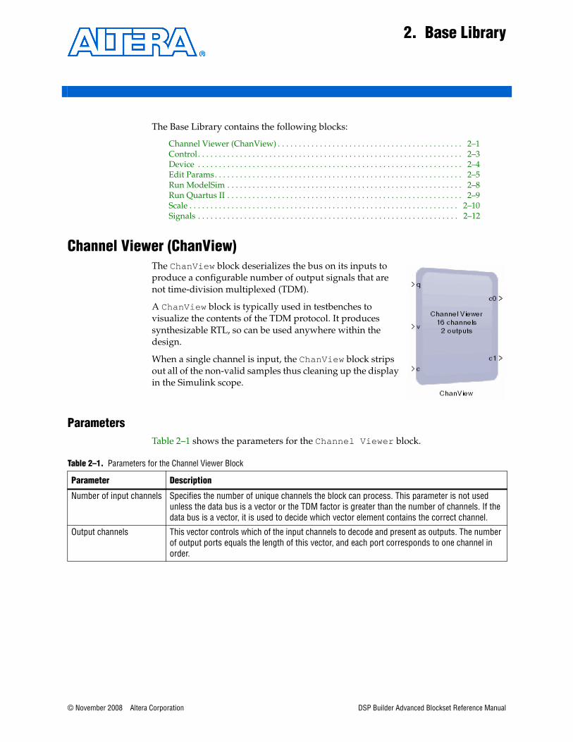
Channel Viewer (ChanView)The ChanView block deserializes the bus on its inputs to produce a configurable number of output signals that are not time-division multiplexed (TDM).
A ChanView block is typically used in testbenches to visualize the contents of the TDM protocol. It produces synthesizable RTL, so can be used anywhere within the design.
When a single channel is input, the ChanView block strips out all of the non-valid samples thus cleaning up the display in the Simulink scope.
ParametersTable 2–1 shows the parameters for the Channel Viewer block.
Table 2–1. Parameters for the Channel Viewer Block
Parameter Description
Number of input channels Specifies the number of unique channels the block can process. This parameter is not used unless the data bus is a vector or the TDM factor is greater than the number of channels. If the data bus is a vector, it is used to decide which vector element contains the correct channel.
Output channels This vector controls which of the input channels to decode and present as outputs. The number of output ports equals the length of this vector, and each port corresponds to one channel in order.
DSP Builder Advanced Blockset Reference Manual
2–2 Chapter 2: Base LibraryChannel Viewer (ChanView)
Port InterfaceTable 2–2 shows the port interface for the Channel Viewer block.
Information MessagesTable 2–3 shows typical Help messages that can be issued for the Channel Viewer block.
Example DesignThe Channel Viewer block is used in many of the demonstration design examples including: demo_ddc, demo_duc, demo_AD9856, demo_wimax_duc, demo_dcic, demo_icic, demo_filters_flow_control, demo_firs, demo_fird, demo_firi, demo_firf, demo_firih, demo_fir_rrc, demo_fir_fractional, demo_nco, demo_mix, demo_complex_mixer, demo_iir, and demo_scale.
f For more information about the demonstration designs, refer to the DSP Builder Advanced Blockset User Guide.
Table 2–2. Port Interface for the Channel Viewer Block
Signal Direction Description
q input The data input to the block. This signal may be a vector.
v input Indicates validity of data input signals. If v is high then the data on the a wire is valid.
c input Indicates channel of data input signals. If v is high, then c indicates which channel the data corresponds to.
cn output Each output is a deserialized version of the channel contained within the time division multiplexed bus. The output value is updated on each clock cycle that has valid data and when the channel matches the required channel.
Table 2–3. Messages for the Channel Viewer Block
Message Example Description
Written on Tue Feb 19 11:25:27 2008 Date and time when this file was run.
Latency is 2 The latency introduced by this block.
Port interface table Lists the port interfaces to the Channel Viewer block.
Resource utilization table Lists the resource utilization for the Channel Viewer block.
DSP Builder Advanced Blockset Reference Manual © November 2008 Altera Corporation
Chapter 2: Base Library 2–3Control
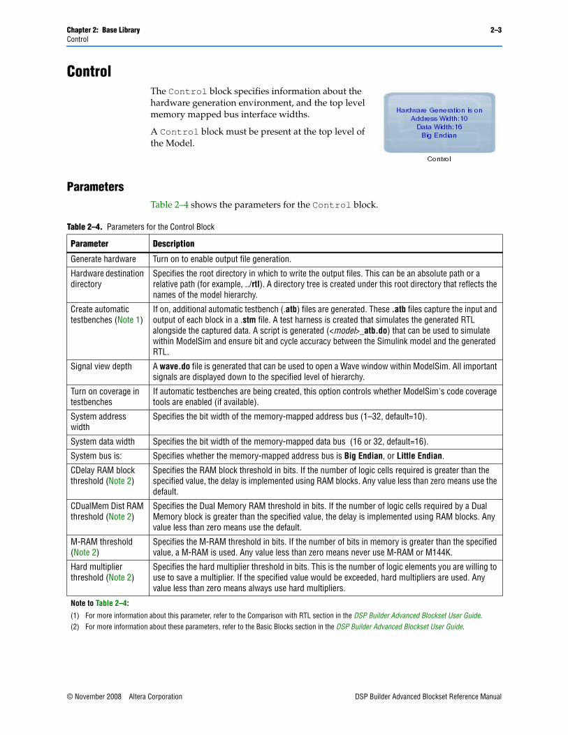
ControlThe Control block specifies information about the hardware generation environment, and the top level memory mapped bus interface widths.
A Control block must be present at the top level of the Model.
ParametersTable 2–4 shows the parameters for the Control block.
Table 2–4. Parameters for the Control Block
Parameter Description
Generate hardware Turn on to enable output file generation.
Hardware destination directory
Specifies the root directory in which to write the output files. This can be an absolute path or a relative path (for example, ../rtl). A directory tree is created under this root directory that reflects the names of the model hierarchy.
Create automatic testbenches (Note 1)
If on, additional automatic testbench (.atb) files are generated. These .atb files capture the input and output of each block in a .stm file. A test harness is created that simulates the generated RTL alongside the captured data. A script is generated (<model>_atb.do) that can be used to simulate within ModelSim and ensure bit and cycle accuracy between the Simulink model and the generated RTL.
Signal view depth A wave.do file is generated that can be used to open a Wave window within ModelSim. All important signals are displayed down to the specified level of hierarchy.
Turn on coverage in testbenches
If automatic testbenches are being created, this option controls whether ModelSim's code coverage tools are enabled (if available).
System address width
Specifies the bit width of the memory-mapped address bus (1–32, default=10).
System data width Specifies the bit width of the memory-mapped data bus (16 or 32, default=16).
System bus is: Specifies whether the memory-mapped address bus is Big Endian, or Little Endian.
CDelay RAM block threshold (Note 2)
Specifies the RAM block threshold in bits. If the number of logic cells required is greater than the specified value, the delay is implemented using RAM blocks. Any value less than zero means use the default.
CDualMem Dist RAM threshold (Note 2)
Specifies the Dual Memory RAM threshold in bits. If the number of logic cells required by a Dual Memory block is greater than the specified value, the delay is implemented using RAM blocks. Any value less than zero means use the default.
M-RAM threshold (Note 2)
Specifies the M-RAM threshold in bits. If the number of bits in memory is greater than the specified value, a M-RAM is used. Any value less than zero means never use M-RAM or M144K.
Hard multiplier threshold (Note 2)
Specifies the hard multiplier threshold in bits. This is the number of logic elements you are willing to use to save a multiplier. If the specified value would be exceeded, hard multipliers are used. Any value less than zero means always use hard multipliers.
Note to Table 2–4:
(1) For more information about this parameter, refer to the Comparison with RTL section in the DSP Builder Advanced Blockset User Guide.(2) For more information about these parameters, refer to the Basic Blocks section in the DSP Builder Advanced Blockset User Guide.
© November 2008 Altera Corporation DSP Builder Advanced Blockset Reference Manual
2–4 Chapter 2: Base LibraryDevice
Information MessagesTable 2–5 shows typical Help messages that can be issued for the Control block.
Example DesignThe Control block is used in all of the demonstration design examples.
f For more information about the demonstration designs, refer to the DSP Builder Advanced Blockset User Guide.
DeviceThe Device block marks a particular Simulink subsystem as the top level of an FPGA device.
This causes the tool to generate project files and scripts that relate to this level of hierarchy. All blocks in subsystems below this level become part of the RTL design. All blocks above this level of hierarchy become part of the testbench.
Multiple Device blocks in non-overlapping subsystems may be used to signify multiple FPGAs will be used for the current design. Device families may be mixed freely.
Table 2–6 shows the parameters for the Device block.
Example DesignThe Device block is used in all of the demonstration design examples.
f For more information about the demonstration designs, refer to the DSP Builder Advanced Blockset User Guide.
Table 2–5. Messages for the Control Block
Message Example Description
Resource utilization table Lists the resource utilization for each subsystem in the current model.
Table 2–6. Parameters for the Device Block
Parameter Description
Device family You can select the required target device family (Stratix, Stratix GX, Stratix II, Stratix II GX, Stratix III, Stratix IV, Cyclone II, or Cyclone III).
Family member Specifies the device member as free-form text or enter AUTO to allow automatic selection. If you enter free-form text, the name must start with EPxxx. For example: EP2C35F484C6.
Speed grade You can select the speed grade for the FPGA target. This helps the tool to balance the hardware size against the resources required to meet the clock frequency set in the Signals Block.
DSP Builder Advanced Blockset Reference Manual © November 2008 Altera Corporation
Chapter 2: Base Library 2–5Edit Params
Edit ParamsThe Edit Params block is used in many of the demonstration design examples although it is not available in the Simulink library browser.
This block is a graphical shortcut to a MATLAB m-script that can be used to setup and initialize your design.
You cannot drag and drop an Edit Params block into your design as it is not a functional block. However, you can create your own Edit Params block if you have created a MATLAB script defining workspace variables that you want to call when the model is loaded and/or initialized. This script should be specified in the PreLoadFcn and InitFcn callbacks which can be accessed by choosing Model Properties from the File menu:
■ To call your script automatically when the model is opened, add a PreloadFcn reference to your script in the Callbacks tab of the Model Properties in Simulink.
■ To call your script automatically at the start of a simulation run, add a InitFcn reference to your script in the Callbacks tab of the Model Properties in Simulink.
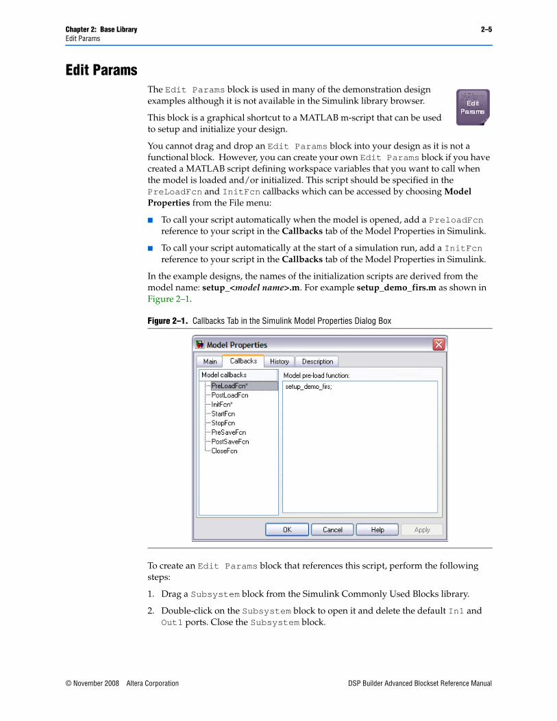
In the example designs, the names of the initialization scripts are derived from the model name: setup_<model name>.m. For example setup_demo_firs.m as shown in Figure 2–1.
To create an Edit Params block that references this script, perform the following steps:
1. Drag a Subsystem block from the Simulink Commonly Used Blocks library.
2. Double-click on the Subsystem block to open it and delete the default In1 and Out1 ports. Close the Subsystem block.
Figure 2–1. Callbacks Tab in the Simulink Model Properties Dialog Box
© November 2008 Altera Corporation DSP Builder Advanced Blockset Reference Manual

2–6 Chapter 2: Base LibraryEdit Params
3. Right-click on the Subsystem block, choose Block Properties and click the Callbacks tab.
4. Choose OpenFcn in the Callback functions list (Figure 2–2).
5. If you have named your script using the format setup_<model name>.m, enter the following functions:
s = sprintf('edit setup_%s', eval('gcs'));
eval(s);
Alternatively, you can explicitly reference a script such as my_script.m by entering a function of the form:
eval(‘edit my_script.m’);
6. Click OK to close the Block Properties dialog box.
7. Rename the Subsystem block EditParams (or any name of your choice).
1 You can optionally hide the block name by right-clicking and choosing Hide Name from the menu.
Figure 2–2. Callbacks in the Subsystem Block Properties Dialog Box
DSP Builder Advanced Blockset Reference Manual © November 2008 Altera Corporation
Chapter 2: Base Library 2–7Edit Params
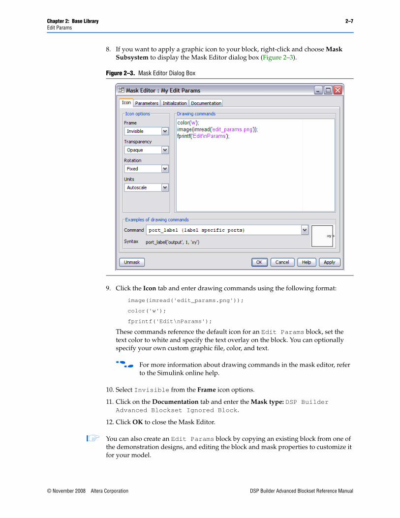
8. If you want to apply a graphic icon to your block, right-click and choose Mask Subsystem to display the Mask Editor dialog box (Figure 2–3).
9. Click the Icon tab and enter drawing commands using the following format:
image(imread('edit_params.png'));
color('w');
fprintf('Edit\nParams');
These commands reference the default icon for an Edit Params block, set the text color to white and specify the text overlay on the block. You can optionally specify your own custom graphic file, color, and text.
f For more information about drawing commands in the mask editor, refer to the Simulink online help.
10. Select Invisible from the Frame icon options.
11. Click on the Documentation tab and enter the Mask type: DSP Builder Advanced Blockset Ignored Block.
12. Click OK to close the Mask Editor.
1 You can also create an Edit Params block by copying an existing block from one of the demonstration designs, and editing the block and mask properties to customize it for your model.
Figure 2–3. Mask Editor Dialog Box
© November 2008 Altera Corporation DSP Builder Advanced Blockset Reference Manual
2–8 Chapter 2: Base LibraryRun ModelSim
UsageDouble-click on the Edit Params block to open the script in the MATLAB text editor.
Example DesignThe Edit Params block is used in many of the demonstration design examples including: demo_ddc, demo_duc, demo_AD9856, demo_dcic, demo_icic, demo_filters_flow_control, demo_firs, demo_fird, demo_firi, demo_firf, demo_firih, demo_fir_rrc, demo_fir_fractional, demo_nco, demo_mix, demo_complex_mixer, demo_fft16_radix2, demo_fft256_radix4, demo_fft_4096_br, demo_fft_8192_br, demo_ifft_4096_natural, and demo_ifft_8192_natural.
f For more information about the demonstration designs, refer to the DSP Builder Advanced Blockset User Guide.
Run ModelSimThe Run ModelSim block loads the design into the ModelSim simulator (if it is available). Simulink components in the testbench are converted to VHDL. If a Simulink component is used that does not have a VHDL description, the simulation may fail.
The following Simulink blocks are translated into VHDL that can be used for simulation:
■ Simulink, Model Verification: Assertion
■ Simulink, Signal Attributes: Data Type Conversion
■ Simulink, Signal Routing: Manual Switch, Mux, Demux, and Selector
■ Simulink, Sources: Constant, Counter Limited, Counter Free-Running, Sine Wave, Ramp, Random Number, Repeating Sequence Stair, and Step
■ Simulink, Math Operations: Complex to Real-Imag, Real-Imag to Complex, and Reshape
■ Signal Processing Blockset, Signal Operations: Zero Pad
f Some options on these blocks may not be supported. For example, not all rounding methods are supported when synthesizing Simulink Data Type Conversion blocks
Other blocks can be used but complete VHDL is not generated. Instead, empty entities are created in the generated VHDL testbench which you can use as templates to complete the VHDL testbench manually. If there are unsupported testbench blocks in your design, there are likely to be many unknowns ('X') in the simulation when you run the generated testbench.
DSP Builder Advanced Blockset Reference Manual © November 2008 Altera Corporation
Chapter 2: Base Library 2–9Run Quartus II
UsageDrop the Run ModelSim block into the top-level of any design. Double-click the Run ModelSim block to launch the ModelSim tool with the user system as the top-level entity. ModelSim automatically starts compiling the design and runs a simulation for the same number of clock cycles as the Simulink simulation.
The simulation is compiled and loaded using the .do scripts that are generated when you run a Simulink simulation. The .do scripts are created in the hardware destination directory specified in the Control block. The generated files and scripts are created in a hierarchy of directories that match the hierarchy of the design and lower level scripts are called from the scripts in the top level directory.
Example DesignThe Run ModelSim block is used in all of the demonstration design examples.
f For more information about the demonstration designs, refer to the DSP Builder Advanced Blockset User Guide.
Run Quartus IIThe Run Quartus II block allows the automatic launching of the user system within the Quartus II software, where the design can be verified for performance and logic utilization.
UsageDrop the Run Quartus II block into the top-level of any design containing an Altera Device block. Double-click the Run Quartus II block to launch the Quartus II software with the user system as the top-level entity.
The .qpf, .qsf, and .qip files for the Quartus II project are created in the design directory that contains the .mdl file. These files contain all required references to the files in the hardware destination directory specified by the Control block that are generated when you run a Simulink simulation.
Once the project has been loaded in the Quartus II software, you should check that the required device settings are selected. You can then compile the design by choosing Start Compilation from the Processing menu.
The project is compiled using the .tcl scripts in the hardware destination directory. The generated files and scripts are created in a hierarchy of directories that match the hierarchy of the design and lower level scripts are called from the scripts in the top level directory.
Example DesignThe Run Quartus II block is used in all of the demonstration design examples.
f For more information about the demonstration designs, refer to the DSP Builder Advanced Blockset User Guide.
© November 2008 Altera Corporation DSP Builder Advanced Blockset Reference Manual
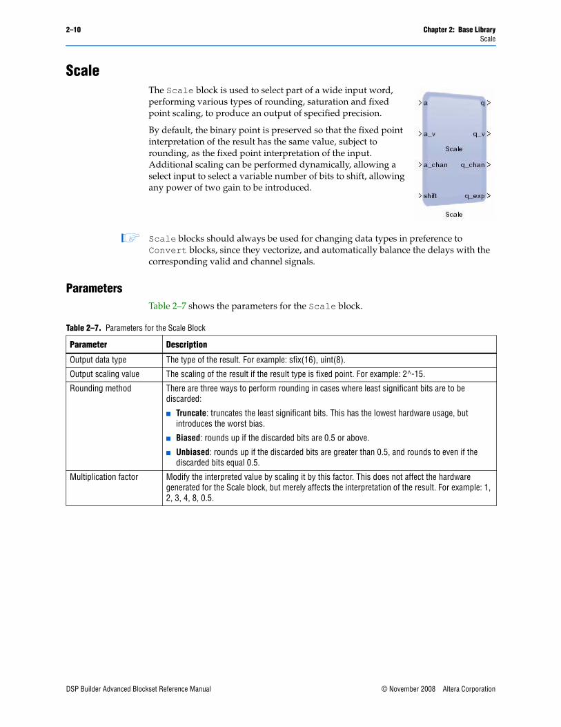
2–10 Chapter 2: Base LibraryScale
ScaleThe Scale block is used to select part of a wide input word, performing various types of rounding, saturation and fixed point scaling, to produce an output of specified precision.
By default, the binary point is preserved so that the fixed point interpretation of the result has the same value, subject to rounding, as the fixed point interpretation of the input. Additional scaling can be performed dynamically, allowing a select input to select a variable number of bits to shift, allowing any power of two gain to be introduced.
1 Scale blocks should always be used for changing data types in preference to Convert blocks, since they vectorize, and automatically balance the delays with the corresponding valid and channel signals.
ParametersTable 2–7 shows the parameters for the Scale block.
Table 2–7. Parameters for the Scale Block
Parameter Description
Output data type The type of the result. For example: sfix(16), uint(8).
Output scaling value The scaling of the result if the result type is fixed point. For example: 2^-15.
Rounding method There are three ways to perform rounding in cases where least significant bits are to be discarded:
■ Truncate: truncates the least significant bits. This has the lowest hardware usage, but introduces the worst bias.
■ Biased: rounds up if the discarded bits are 0.5 or above.
■ Unbiased: rounds up if the discarded bits are greater than 0.5, and rounds to even if the discarded bits equal 0.5.
Multiplication factor Modify the interpreted value by scaling it by this factor. This does not affect the hardware generated for the Scale block, but merely affects the interpretation of the result. For example: 1, 2, 3, 4, 8, 0.5.
DSP Builder Advanced Blockset Reference Manual © November 2008 Altera Corporation
Chapter 2: Base Library 2–11Scale
Port InterfaceTable 2–8 shows the port interface for the Scale block.
Information MessagesTable 2–9 shows typical Help messages that can be issued for the Scale block.
Saturation method There are three ways to perform saturation in the cases where most significant bits are to be discarded:
■ None: No saturation is performed.
■ Asymmetric: The range of the number produced occupies the whole of the two's complement range (for example -1.0 to 0.999). There is one more negative number available, so this will introduce a slight bias.
■ Symmetric: The range of the result is clipped to between symmetrical boundaries (for example -0.999 and 0.999). This ensures no bias enters the dataflow.
Number of bits to shift left
A scalar or a vector that determines the gain of the result. A positive number indicates that the scale block introduces a gain to the input. A negative number means that the output signal is attenuated. A vector of gains allows the shift input signal to select which gain to use on a cycle per cycle basis. The value of the shift integer is used to perform zero-based indexing of the vector. For example: 2, -4, [0 1 2 3]
Table 2–7. Parameters for the Scale Block
Parameter Description
Table 2–8. Port Interface for the Scale Block
Signal Direction Description
a input The data input to the block. If more channels are requested than can fit onto a single bus, then this signal is a vector. The bit width is inherited from the input wire.
a_v input Indicates validity of data input signals. If a_v is high then the data on the a wire is valid.
a_chan input Indicates channel of data input signals. If a_v is high, then a_chan indicates which channel the data corresponds to.
shift input Indicates which element of the zero-based shift vector to use.
q output The data output from the block. If more channels are requested than can fit onto a single bus, then this signal is a vector. The bit width is calculated as a function of the input bit width and the parameterization.
q_v output Indicates validity of data output signals.
q_chan output Indicates channel of data output signals.
q_exp output Indicates whether the output sample has saturated or overflowed.
Table 2–9. Messages for the Scale Block
Message Example Description
Written on Tue Feb 19 11:25:27 2008 Date and time when this file was run.
Number of physical buses: 4 Depending on the input data rate, the number of data wires needed to carry the input data may be more than 1.
Calculated bit width of output stage: 16 The bit width of the (vectorized) data output.
Latency is 2 The latency introduced by this block.
Parameters table Lists the current rounding and saturation modes.
© November 2008 Altera Corporation DSP Builder Advanced Blockset Reference Manual
2–12 Chapter 2: Base LibrarySignals
Example DesignAn example of using the Scale block is shown in the demo_scale demonstration design. It is also used in several of the other demonstration designs including: demo_ddc, demo_duc, demo_AD9856, demo_filters_flow_control, demo_wimax_duc, and demo_fir_fractional.
f For more information about the demonstration designs, refer to the DSP Builder Advanced Blockset User Guide.
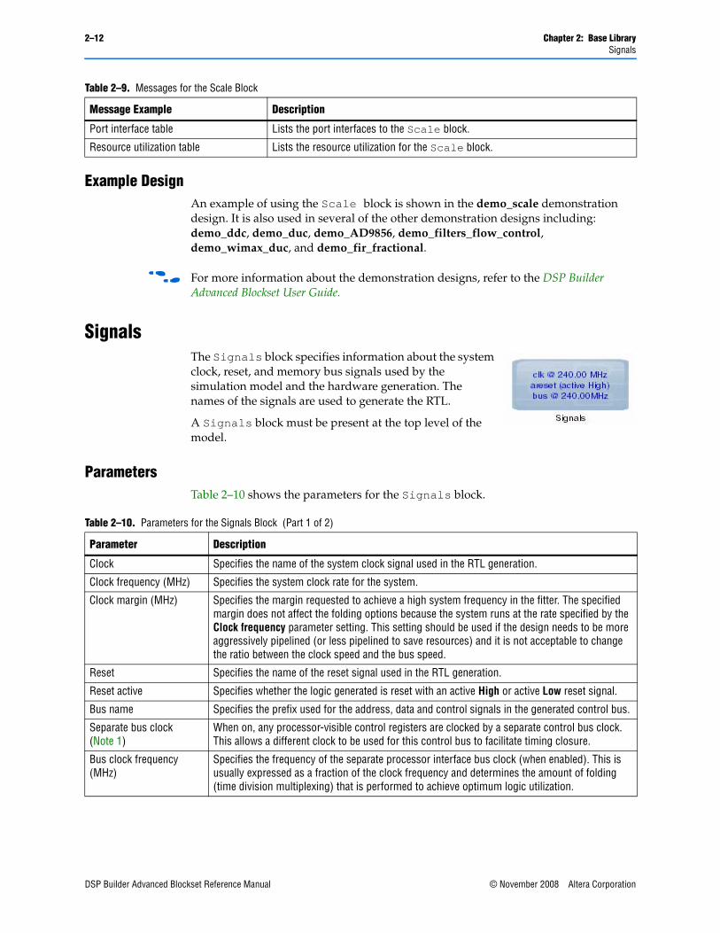
SignalsThe Signals block specifies information about the system clock, reset, and memory bus signals used by the simulation model and the hardware generation. The names of the signals are used to generate the RTL.
A Signals block must be present at the top level of the model.
ParametersTable 2–10 shows the parameters for the Signals block.
Port interface table Lists the port interfaces to the Scale block.
Resource utilization table Lists the resource utilization for the Scale block.
Table 2–9. Messages for the Scale Block
Message Example Description
Table 2–10. Parameters for the Signals Block (Part 1 of 2)
Parameter Description
Clock Specifies the name of the system clock signal used in the RTL generation.
Clock frequency (MHz) Specifies the system clock rate for the system.
Clock margin (MHz) Specifies the margin requested to achieve a high system frequency in the fitter. The specified margin does not affect the folding options because the system runs at the rate specified by the Clock frequency parameter setting. This setting should be used if the design needs to be more aggressively pipelined (or less pipelined to save resources) and it is not acceptable to change the ratio between the clock speed and the bus speed.
Reset Specifies the name of the reset signal used in the RTL generation.
Reset active Specifies whether the logic generated is reset with an active High or active Low reset signal.
Bus name Specifies the prefix used for the address, data and control signals in the generated control bus.
Separate bus clock (Note 1)
When on, any processor-visible control registers are clocked by a separate control bus clock. This allows a different clock to be used for this control bus to facilitate timing closure.
Bus clock frequency (MHz)
Specifies the frequency of the separate processor interface bus clock (when enabled). This is usually expressed as a fraction of the clock frequency and determines the amount of folding (time division multiplexing) that is performed to achieve optimum logic utilization.
DSP Builder Advanced Blockset Reference Manual © November 2008 Altera Corporation
Chapter 2: Base Library 2–13Signals
Information MessagesTable 2–11 shows typical Help messages that can be issued for the Signals block.
Example DesignThe Signals block is used in all of the demonstration design examples.
f For more information about the demonstration designs, refer to the DSP Builder Advanced Blockset User Guide.
Bus clock synchronous with system clock
When on, the bus clock is synchronous with the system clock.
Note to Table 2–10:
(1) This option should be off when using Cyclone families because these devices have limited multiple clock support in block RAMs and do not support a separate bus clock.
Table 2–10. Parameters for the Signals Block (Part 2 of 2)
Parameter Description
Table 2–11. Messages for the Signals Block
Message Example Description
Parameters table Lists the system clock name, system clock rate, fitter target frequency, reset name and reset active parameters for the current model.
© November 2008 Altera Corporation DSP Builder Advanced Blockset Reference Manual

2–14 Chapter 2: Base LibrarySignals
DSP Builder Advanced Blockset Reference Manual © November 2008 Altera Corporation
© November 2008 Altera Corporation
3. Filter Library
The Filter Library contains the following blocks:
Single Rate FIR . . . . . . . . . . . . . . . . . . . . . . . . . . . . . . . . . . . . . . . . . . . . . . . . . . . . . . . . 3–4Interpolating FIR . . . . . . . . . . . . . . . . . . . . . . . . . . . . . . . . . . . . . . . . . . . . . . . . . . . . . . 3–7Decimating FIR. . . . . . . . . . . . . . . . . . . . . . . . . . . . . . . . . . . . . . . . . . . . . . . . . . . . . . . 3–11Fractional Rate FIR. . . . . . . . . . . . . . . . . . . . . . . . . . . . . . . . . . . . . . . . . . . . . . . . . . . . 3–15Interpolating CIC . . . . . . . . . . . . . . . . . . . . . . . . . . . . . . . . . . . . . . . . . . . . . . . . . . . . . 3–19Decimating CIC . . . . . . . . . . . . . . . . . . . . . . . . . . . . . . . . . . . . . . . . . . . . . . . . . . . . . . 3–23
FIR and CIC FiltersThis chapter describes blocks that implement several finite impulse response (FIR) and cascaded integrator comb (CIC) filters. The filters share many common features and use advanced high level synthesis techniques to generate filters with higher clock speeds, lower logic, multiplier and memory counts. Using these high clock rates allows you to reduce your costs by choosing smaller FPGAs.
Common Features■ Filter length 1–256 taps
■ Data input bit width 2–32 bits
■ Data output bit width 4–64 bits
■ Multi-channel (up to 1024 channels)
■ Powerful MATLAB integration
■ Simulink fixed point integration
■ Automatic pipelining
■ Plug and play connectivity
■ Simplified timing closure
1 Each channel is an independent data source. In an IF Modem design, two channels are required for the complex pair from each antenna.
Basic FIR Filter OperationThe basic convolution operation performed by a single rate FIR filter is shown in Equation 3–1.
Equation 3–1.
where k = 0, 1,2, ..., n-1yk an
n 0=
n 1=
∑ Xk n–×=
DSP Builder Advanced Blockset Reference Manual
3–2 Chapter 3: Filter LibraryFIR and CIC Filters
At each sample time k, the new output y, is calculated by multiplying coefficients a, by the recent past values of the input x.
Half-Band and L-Band Nyquist FIR FiltersSome filtering functions can use a half-band filter where nearly half of the coefficients are zero. The half-band support uses these extra zeros to further reduce the number of multipliers, and reduce the filter cost.
The generalized form of these filters are L-band Nyquist filters, where every Lth coefficient is zero counting out from the center tap. These structures are also supported and can often reduce the number of multipliers required in a filter.
Automatic PipeliningThe required system clock frequency, and the device family and speed grade are used to determine the maximum logic depth permitted in the output RTL. Functions such as adders are pipelined by splitting them into multiple sections with a registered carry between them. This decreases the logic depth allowing higher frequency operation.
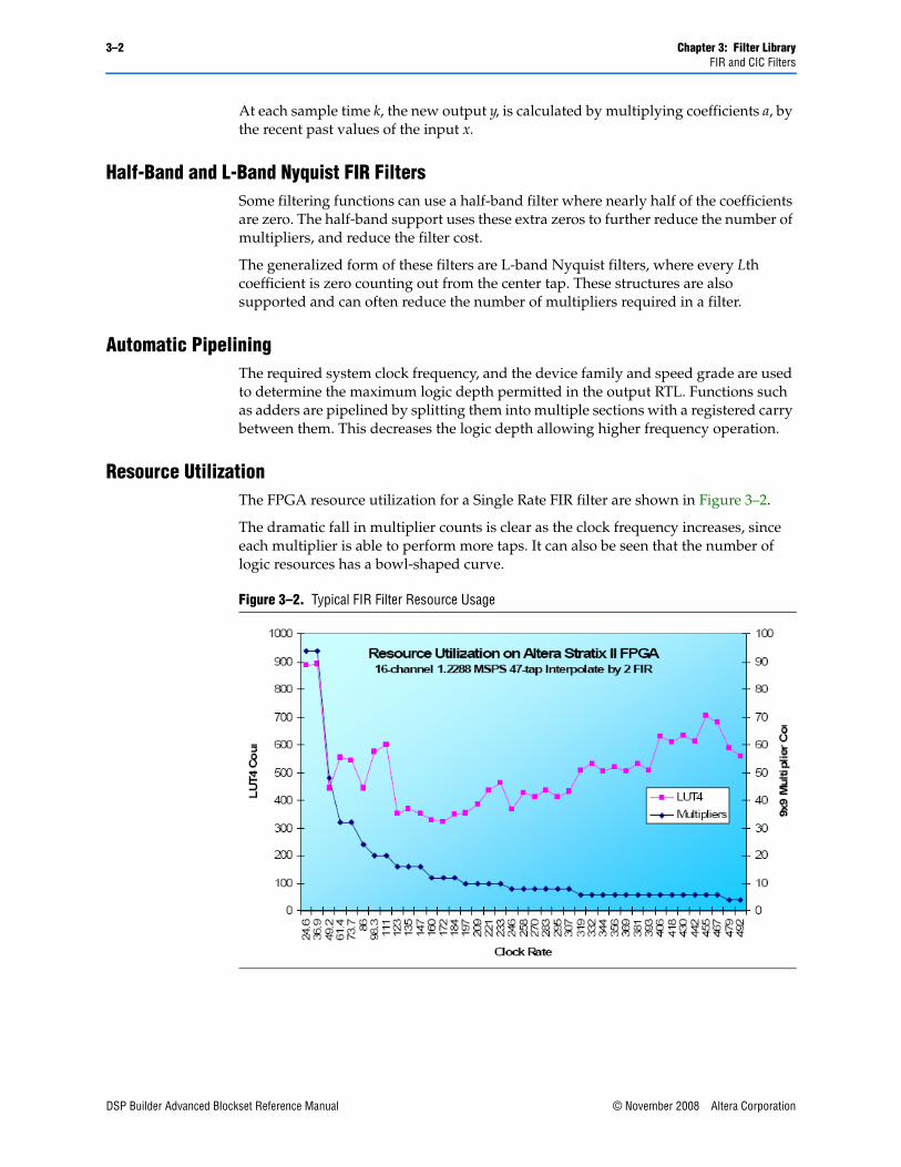
Resource UtilizationThe FPGA resource utilization for a Single Rate FIR filter are shown in Figure 3–2.
The dramatic fall in multiplier counts is clear as the clock frequency increases, since each multiplier is able to perform more taps. It can also be seen that the number of logic resources has a bowl-shaped curve.
Figure 3–2. Typical FIR Filter Resource Usage
DSP Builder Advanced Blockset Reference Manual © November 2008 Altera Corporation
Chapter 3: Filter Library 3–3FIR and CIC Filters
This reflects the fact that at low frequencies there are more adders to cope with the extra multipliers used, while at the high frequencies long adders have been pipelined into shorter sections, to meet the system clock frequency requirement. Some typical results are shown in the block descriptions for each type of filter.
High Speed OperationBecause the filter generator is responsive to the system clock frequency, timing closure is much easier to achieve. The heuristics used by the generator ensure that the logic generated is capable of running at the desired system clock frequency on the FPGA. Timing closure can be aided simply by dialing in a little more clock margin, resulting in additional pipelining to shorten critical paths.
The maximum clock frequencies are governed by the FPGA structures such as internal multiplier and memory delays.
ScalabilityIn some cases, the aggregate sample rate for all channels may be higher than the system clock rate. In these cases, the filter has multiple input and/or output buses to carry the additional data. This is modelled in the Simulink block by increasing the vector width of the data signals.
ParameterizationThe main parameters for a filter are determined by the system specification, such as the channel count, and sample rates. The remaining parameters such as data widths and system clock rates are inferred from the enclosing Simulink model. This has the advantage that parameter changes ripple through a design, changing the system performance without having to update numerous different cores. Additionally, since all parameters can be expressed as MATLAB expressions, whole systems can be readily parameterized.
The sophisticated hardware generation techniques used allow the creation of efficient filters with combinations of parameters, such as a symmetric 3-band FIR filter with 7 channels and 100 cycles to execute a sample from each channel. Hardware generation is fast enough to be run on-the-fly with every Simulink simulation, so that the edit simulation loop time is much reduced, improving productivity.
Filter coefficients can be generated using a MATLAB function and reloaded at run-time using the memory mapped interface.
Coefficient GenerationFilter coefficients can be generated using a MATLAB function. For example, the Simulink fixed-point object fi(fir1(49, 0.3),1,18,19). Coefficients can be reloaded at run-time using the memory-mapped interface registers.
ChannelizationThe input channel data format and output data channel format used by a FIR or CIC filter are shown in the generated help page for the block after you have run a Simulink simulation.
© November 2008 Altera Corporation DSP Builder Advanced Blockset Reference Manual
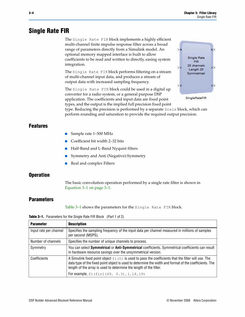
3–4 Chapter 3: Filter LibrarySingle Rate FIR
Single Rate FIRThe Single Rate FIR block implements a highly efficient multi-channel finite impulse response filter across a broad range of parameters directly from a Simulink model. An optional memory mapped interface is built to allow coefficients to be read and written to directly, easing system integration.
The Single Rate FIR block performs filtering on a stream of multi-channel input data, and produces a stream of output data with increased sampling frequency.
The Single Rate FIR block could be used in a digital up converter for a radio system, or a general purpose DSP application. The coefficients and input data are fixed point types, and the output is the implied full precision fixed point type. Reducing the precision is performed by a separate Scale block, which can perform rounding and saturation to provide the required output precision.
Features■ Sample rate 1–500 MHz
■ Coefficient bit width 2–32 bits
■ Half-Band and L-Band Nyquist filters
■ Symmetry and Anti (Negative)-Symmetry
■ Real and complex Filters
OperationThe basic convolution operation performed by a single rate filter is shown in Equation 3–1 on page 3–1.
ParametersTable 3–1 shows the parameters for the Single Rate FIR block.
Table 3–1. Parameters for the Single Rate FIR Block (Part 1 of 2)
Parameter Description
Input rate per channel Specifies the sampling frequency of the input data per channel measured in millions of samples per second (MSPS).
Number of channels Specifies the number of unique channels to process.
Symmetry You can select Symmetrical or Anti-Symmetrical coefficients. Symmetrical coefficients can result in hardware resource savings over the unsymmetrical version.
Coefficients A Simulink fixed point object fi(0) is used to pass the coefficients that the filter will use. The data type of the fixed point object is used to determine the width and format of the coefficients. The length of the array is used to determine the length of the filter.
For example, fi(fir1(49, 0.3),1,18,19)
DSP Builder Advanced Blockset Reference Manual © November 2008 Altera Corporation
Chapter 3: Filter Library 3–5Single Rate FIR
Filter CoefficientsYou can change coefficients in the filter on the fly, by writing to the memory mapped coefficients. There is no need to create custom logic to deal with awkward update schemes.
The base address of the memory-mapped coefficients can be set using the Base address parameter and the filter coefficients set by entering a Simulink fixed point array into the Coefficients parameter. A vector of coefficients can be generated either by entering an array of numbers, or using one of the many MATLAB functions to build the required coefficients.
f For more information about Simulink fixed point objects and MATLAB functions, refer to the MATLAB help.
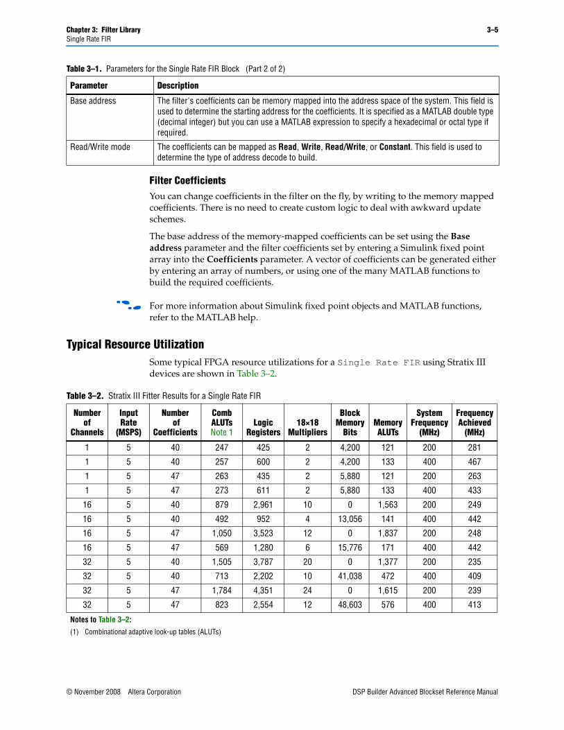
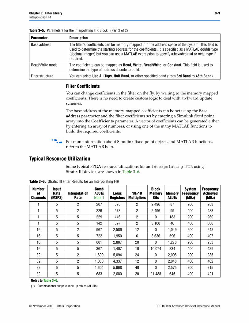
Typical Resource UtilizationSome typical FPGA resource utilizations for a Single Rate FIR using Stratix III devices are shown in Table 3–2.
Base address The filter's coefficients can be memory mapped into the address space of the system. This field is used to determine the starting address for the coefficients. It is specified as a MATLAB double type (decimal integer) but you can use a MATLAB expression to specify a hexadecimal or octal type if required.
Read/Write mode The coefficients can be mapped as Read, Write, Read/Write, or Constant. This field is used to determine the type of address decode to build.
Table 3–1. Parameters for the Single Rate FIR Block (Part 2 of 2)
Parameter Description
Table 3–2. Stratix III Fitter Results for a Single Rate FIR
Number of
Channels
Input Rate
(MSPS)
Number of
Coefficients
Comb ALUTs Note 1
Logic Registers
18×18 Multipliers
Block Memory
BitsMemory ALUTs
System Frequency
(MHz)
Frequency Achieved
(MHz)
1 5 40 247 425 2 4,200 121 200 281
1 5 40 257 600 2 4,200 133 400 467
1 5 47 263 435 2 5,880 121 200 263
1 5 47 273 611 2 5,880 133 400 433
16 5 40 879 2,961 10 0 1,563 200 249
16 5 40 492 952 4 13,056 141 400 442
16 5 47 1,050 3,523 12 0 1,837 200 248
16 5 47 569 1,280 6 15,776 171 400 442
32 5 40 1,505 3,787 20 0 1,377 200 235
32 5 40 713 2,202 10 41,038 472 400 409
32 5 47 1,784 4,351 24 0 1,615 200 239
32 5 47 823 2,554 12 48,603 576 400 413
Notes to Table 3–2:
(1) Combinational adaptive look-up tables (ALUTs)
© November 2008 Altera Corporation DSP Builder Advanced Blockset Reference Manual
3–6 Chapter 3: Filter LibrarySingle Rate FIR
Port InterfaceTable 3–3 shows the port interface for the Single Rate FIR block.
Information MessagesWhenever the model runs within Simulink, messages are issued that are specific to the Single Rate FIR block. For example, the amount of folding achieved is reported. Some examples are shown in Table 3–4.
Table 3–3. Port Interface for the Single Rate FIR Block
Signal Direction Description
a input The data input to the block. If more channels are requested than can fit on a single bus, this signal is a vector. The bit width is inherited from the input wire.
v input Indicates validity of the data input signals. If v is high, the data on the a wire is valid.
c input Indicates channel of data input signals. If v is high, then c indicates which channel the data corresponds to.
q output The data output from the block. If more channels are requested than can fit on a single bus, this signal is a vector. The bit width is a function of the input bit width and the parameterization.
v output Indicates validity of data output signals. Note 1
c output Indicates channel of data output signals. Note 1
Notes to Table 3–3:
(1) The output data can be non-zero when v is low.
Table 3–4. Messages for the Single Rate FIR Block (Part 1 of 2)
Message Example Description
Written on Tue Feb 19 13:04:04 2008 Date and time when this file was run.
Single Rate Filter Version: $Revision: 1.111 $
The version number and revision for the Single Rate FIR Filter (Version 1, revision 111 in this example).
Number of physical input buses: 1 Depending on the input data rate, the number of wires needed to carry the input data may be more than 1. If so, the comb sections of the filter are duplicated (vectorized) to satisfy the data rate requirement.
Number of physical output buses: 2 Depending on the output data rate, the number of wires needed to carry the output data may be more than 1. If so, the output wires are duplicated (vectorized) to satisfy the data rate requirement. The output data rate is the product of the input rate and the interpolation rate.
Calculated bit width of output stage: 26 This is the bit width of the (vectorized) data output from the filter.
Number of different phases: 1 The number of different phases.
Implementation Folding: 3 The number of times that each multiplier is used per sample to reduce the implementation size.
Filter Utilization: 48/50 (96.00%) For some sample rates, it is necessary to stall the filter internally for a number of cycles. The number of cycles used for active calculation is shown with the number of cycles determined by the sample rate relative to the system clock frequency.
Tap Utilization: 25/27 (92.59%) When some filters are folded there may be unused extra taps. The extra taps may be used to increase the filter length with no hardware resource increase.
Latency is 9 The latency introduced by this block.
DSP Builder Advanced Blockset Reference Manual © November 2008 Altera Corporation
Chapter 3: Filter Library 3–7Interpolating FIR
Example DesignAn example of using the Single Rate FIR block is shown in the demo_firs demonstration design. It is also used in the demo_AD9856, and demo_wimax_duc demonstration designs.
f For more information about the demonstration designs, refer to the DSP Builder Advanced Blockset User Guide.
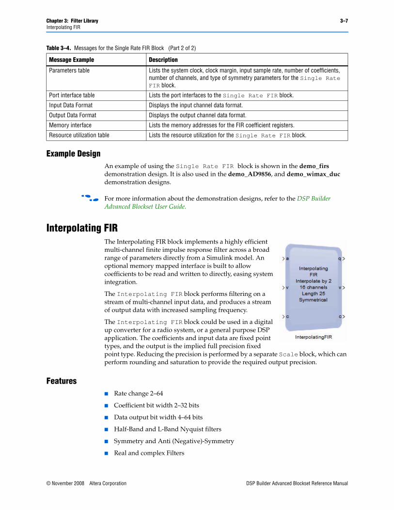
Interpolating FIRThe Interpolating FIR block implements a highly efficient multi-channel finite impulse response filter across a broad range of parameters directly from a Simulink model. An optional memory mapped interface is built to allow coefficients to be read and written to directly, easing system integration.
The Interpolating FIR block performs filtering on a stream of multi-channel input data, and produces a stream of output data with increased sampling frequency.
The Interpolating FIR block could be used in a digital up converter for a radio system, or a general purpose DSP application. The coefficients and input data are fixed point types, and the output is the implied full precision fixed point type. Reducing the precision is performed by a separate Scale block, which can perform rounding and saturation to provide the required output precision.
Features■ Rate change 2–64
■ Coefficient bit width 2–32 bits
■ Data output bit width 4–64 bits
■ Half-Band and L-Band Nyquist filters
■ Symmetry and Anti (Negative)-Symmetry
■ Real and complex Filters
Parameters table Lists the system clock, clock margin, input sample rate, number of coefficients, number of channels, and type of symmetry parameters for the Single Rate FIR block.
Port interface table Lists the port interfaces to the Single Rate FIR block.
Input Data Format Displays the input channel data format.
Output Data Format Displays the output channel data format.
Memory interface Lists the memory addresses for the FIR coefficient registers.
Resource utilization table Lists the resource utilization for the Single Rate FIR block.
Table 3–4. Messages for the Single Rate FIR Block (Part 2 of 2)
Message Example Description
© November 2008 Altera Corporation DSP Builder Advanced Blockset Reference Manual
3–8 Chapter 3: Filter LibraryInterpolating FIR
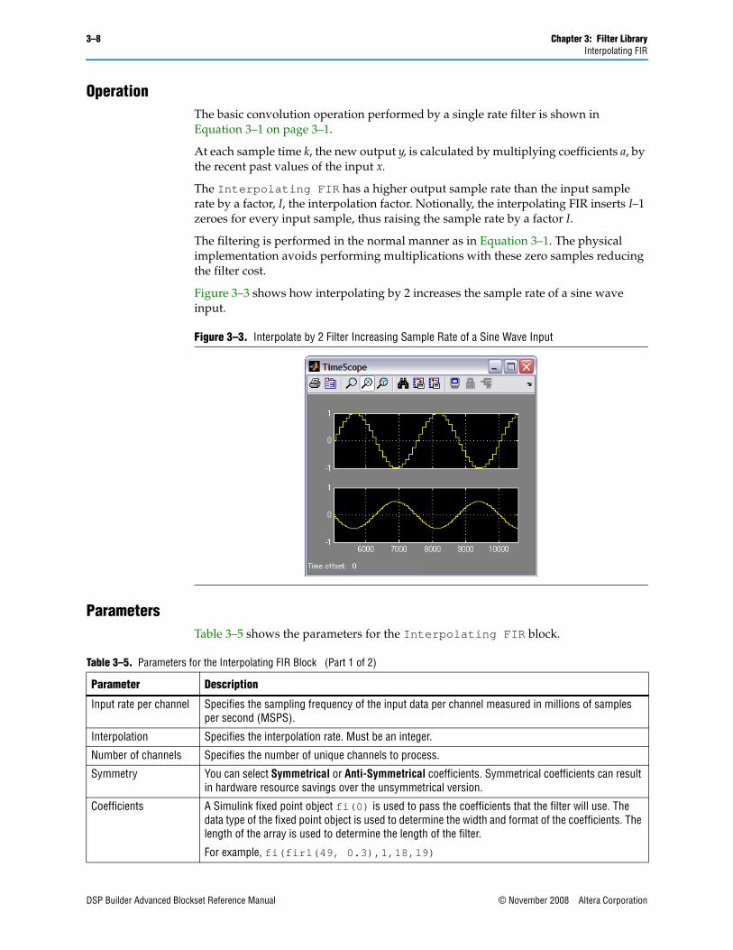
OperationThe basic convolution operation performed by a single rate filter is shown in Equation 3–1 on page 3–1.
At each sample time k, the new output y, is calculated by multiplying coefficients a, by the recent past values of the input x.
The Interpolating FIR has a higher output sample rate than the input sample rate by a factor, I, the interpolation factor. Notionally, the interpolating FIR inserts I–1 zeroes for every input sample, thus raising the sample rate by a factor I.
The filtering is performed in the normal manner as in Equation 3–1. The physical implementation avoids performing multiplications with these zero samples reducing the filter cost.
Figure 3–3 shows how interpolating by 2 increases the sample rate of a sine wave input.
ParametersTable 3–5 shows the parameters for the Interpolating FIR block.
Figure 3–3. Interpolate by 2 Filter Increasing Sample Rate of a Sine Wave Input
Table 3–5. Parameters for the Interpolating FIR Block (Part 1 of 2)
Parameter Description
Input rate per channel Specifies the sampling frequency of the input data per channel measured in millions of samples per second (MSPS).
Interpolation Specifies the interpolation rate. Must be an integer.
Number of channels Specifies the number of unique channels to process.
Symmetry You can select Symmetrical or Anti-Symmetrical coefficients. Symmetrical coefficients can result in hardware resource savings over the unsymmetrical version.
Coefficients A Simulink fixed point object fi(0) is used to pass the coefficients that the filter will use. The data type of the fixed point object is used to determine the width and format of the coefficients. The length of the array is used to determine the length of the filter.
For example, fi(fir1(49, 0.3),1,18,19)
DSP Builder Advanced Blockset Reference Manual © November 2008 Altera Corporation
Chapter 3: Filter Library 3–9Interpolating FIR
Filter CoefficientsYou can change coefficients in the filter on the fly, by writing to the memory mapped coefficients. There is no need to create custom logic to deal with awkward update schemes.
The base address of the memory-mapped coefficients can be set using the Base address parameter and the filter coefficients set by entering a Simulink fixed point array into the Coefficients parameter. A vector of coefficients can be generated either by entering an array of numbers, or using one of the many MATLAB functions to build the required coefficients.
f For more information about Simulink fixed point objects and MATLAB functions, refer to the MATLAB help.
Typical Resource UtilizationSome typical FPGA resource utilizations for an Interpolating FIR using Stratix III devices are shown in Table 3–6.
Base address The filter's coefficients can be memory mapped into the address space of the system. This field is used to determine the starting address for the coefficients. It is specified as a MATLAB double type (decimal integer) but you can use a MATLAB expression to specify a hexadecimal or octal type if required.
Read/Write mode The coefficients can be mapped as Read, Write, Read/Write, or Constant. This field is used to determine the type of address decode to build.
Filter structure You can select Use All Taps, Half Band, or other specified band (from 3rd Band to 46th Band).
Table 3–5. Parameters for the Interpolating FIR Block (Part 2 of 2)
Parameter Description
Table 3–6. Stratix III Fitter Results for an Interpolating FIR
Number of
Channels
Input Rate
(MSPS)Interpolation
Rate
Comb ALUTs Note 1
Logic Registers
18×18 Multipliers
Block Memory
BitsMemory ALUTs
System Frequency
(MHz)
Frequency Achieved
(MHz)
1 5 2 207 395 2 2,496 87 200 283
1 5 2 226 573 2 2,496 99 400 483
1 5 5 229 446 2 0 183 200 260
1 5 5 142 397 2 3,100 46 400 506
16 5 2 967 2,586 12 0 1,049 200 248
16 5 5 722 1,950 6 8,636 596 400 407
16 5 5 801 2,887 20 0 1,278 200 233
16 5 5 367 1,407 10 10,074 334 400 429
32 5 2 1,899 5,094 24 0 2,098 200 235
32 5 2 1,050 4,337 12 0 2,048 400 402
32 5 5 1,604 5,668 40 0 2,575 200 215
32 5 5 683 2,680 20 21,488 645 400 421
Notes to Table 3–6:
(1) Combinational adaptive look-up tables (ALUTs)
© November 2008 Altera Corporation DSP Builder Advanced Blockset Reference Manual
3–10 Chapter 3: Filter LibraryInterpolating FIR
Port InterfaceTable 3–7 shows the port interface for the Interpolating FIR block.
Information MessagesWhenever the model runs within Simulink, messages are issued that are specific to the Interpolating FIR block. For example, the amount of folding achieved is reported. Some examples are shown in Table 3–8.
Table 3–7. Port Interface for the Interpolating FIR Block
Signal Direction Description
a input The data input to the block. If more channels are requested than can fit on a single bus, this signal is a vector. The bit width is inherited from the input wire.
v input Indicates validity of the data input signals. If v is high, the data on the a wire is valid.
c input Indicates channel of data input signals. If v is high, then c indicates which channel the data corresponds to.
q output The data output from the block. If more channels are requested than can fit on a single bus, this signal is a vector. The bit width is a function of the input bit width and the parameterization.
v output Indicates validity of data output signals. Note 1
c output Indicates channel of data output signals. Note 1
Notes to Table 3–7:
(1) The output data can be non-zero when v is low.
Table 3–8. Messages for the Interpolating FIR Block (Part 1 of 2)
Message Example Description
Written on Tue Feb 19 12:52:32 2008 Date and time when this file was run.
Interpolating Filter Version: $Revision: 1.111 $
The version number and revision for the Interpolating FIR Filter (Version 1, revision 111 in this example).
Number of physical input buses: 1 Depending on the input data rate, the number of wires needed to carry the input data may be more than 1. If so, the comb sections of the filter are duplicated (vectorized) to satisfy the data rate requirement.
Number of physical output buses: 2 Depending on the output data rate, the number of wires needed to carry the output data may be more than 1. If so, the output wires are duplicated (vectorized) to satisfy the data rate requirement. The output data rate is the product of the input rate and the interpolation rate.
Calculated bit width of output stages: 26 This is the bit width of the (vectorized) data output from the filter.
Number of different phases: 1 The number of different phases.
Implementation Folding: 3 The number of times that each multiplier is used per sample to reduce the implementation size.
Filter Utilization: 48/50 (96.00%) For some sample rates, it is necessary to stall the filter internally for a number of cycles. The number of cycles used for active calculation is shown with the number of cycles determined by the sample rate relative to the system clock frequency.
Tap Utilization: 25/27 (92.59%) When some filters are folded there may be unused extra taps. The extra taps may be used to increase the filter length with no hardware resource increase.
Latency is 9 The latency introduced by this block.
DSP Builder Advanced Blockset Reference Manual © November 2008 Altera Corporation
Chapter 3: Filter Library 3–11Decimating FIR
Example DesignAn example of using the Interpolating FIR block is shown in the demo_firi demonstration design. It is also used in the demo_firih, demo_fir_fractional, demo_filters_flow_control, demo_duc, demo_AD9856, and demo_wimax_duc, demonstration designs.
f For more information about the demonstration designs, refer to the DSP Builder Advanced Blockset User Guide.
Decimating FIRThe Decimating FIR block implements a highly efficient multi-channel finite impulse response filter across a broad range of parameters directly from a Simulink model. An optional memory mapped interface is built to allow coefficients to be read and written to directly, easing system integration.
The Decimating FIR block performs filtering on a stream of multi-channel input data, and produces a stream of output data with increased sampling frequency.
The Decimating FIR block could be used in a digital down converter for a radio system, or a general purpose DSP application. The coefficients and input data are fixed point types, and the output is the implied full precision fixed point type. Reducing the precision is performed by a separate Scale block, which can perform rounding and saturation to provide the required output precision.
Features■ Rate change 2–64 MHz
■ Coefficient bit width 2–32 bits
■ Half-Band and L-Band Nyquist filters
■ Symmetry and Anti (Negative)-Symmetry
■ Real and complex Filters
Parameters table Lists the system clock, clock margin, input sample rate, number of coefficients, interpolation rate, number of channels, and type of symmetry parameters for the Interpolating FIR block.
Port interface table Lists the port interfaces to the Interpolating FIR block.
Input Data Format Displays the input channel data format.
Output Data Format Displays the output channel data format.
Memory interface Lists the memory addresses for the FIR coefficient registers.
Resource utilization table Lists the resource utilization for the Interpolating FIR block.
Table 3–8. Messages for the Interpolating FIR Block (Part 2 of 2)
Message Example Description
© November 2008 Altera Corporation DSP Builder Advanced Blockset Reference Manual
3–12 Chapter 3: Filter LibraryDecimating FIR
OperationThe basic convolution operation performed by a single rate filter is shown in Equation 3–1 on page 3–1.
At each sample time k, the new output y, is calculated by multiplying coefficients a, by the recent past values of the input x.
The Decimating FIR has a lower output sample rate than the input sample rate by a factor, D, the decimation factor. Notionally, the decimating FIR discards D–1 out of D output samples, thus lowering the sample rate by a factor D.
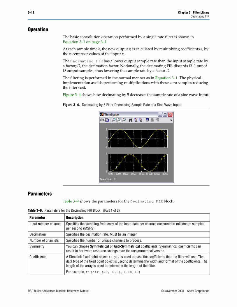
The filtering is performed in the normal manner as in Equation 3–1. The physical implementation avoids performing multiplications with these zero samples reducing the filter cost.
Figure 3–4 shows how decimating by 5 decreases the sample rate of a sine wave input.
ParametersTable 3–9 shows the parameters for the Decimating FIR block.
Figure 3–4. Decimating by 5 Filter Decreasing Sample Rate of a Sine Wave Input
Table 3–9. Parameters for the Decimating FIR Block (Part 1 of 2)
Parameter Description
Input rate per channel Specifies the sampling frequency of the input data per channel measured in millions of samples per second (MSPS).
Decimation Specifies the decimation rate. Must be an integer.
Number of channels Specifies the number of unique channels to process.
Symmetry You can choose Symmetrical or Anti-Symmetrical coefficients. Symmetrical coefficients can result in hardware resource savings over the unsymmetrical version.
Coefficients A Simulink fixed point object fi(0) is used to pass the coefficients that the filter will use. The data type of the fixed point object is used to determine the width and format of the coefficients. The length of the array is used to determine the length of the filter.
For example, fi(fir1(49, 0.3),1,18,19)
DSP Builder Advanced Blockset Reference Manual © November 2008 Altera Corporation
Chapter 3: Filter Library 3–13Decimating FIR
Filter CoefficientsYou can change coefficients in the filter on the fly, by writing to the memory mapped coefficients. There is no need to create custom logic to deal with awkward update schemes.
The base address of the memory-mapped coefficients can be set using the Base address parameter and the filter coefficients set by entering a Simulink fixed point array into the Coefficients parameter. A vector of coefficients can be generated either by entering an array of numbers, or using one of the many MATLAB functions to build the required coefficients.
f For more information about Simulink fixed point objects and MATLAB functions, refer to the MATLAB help.
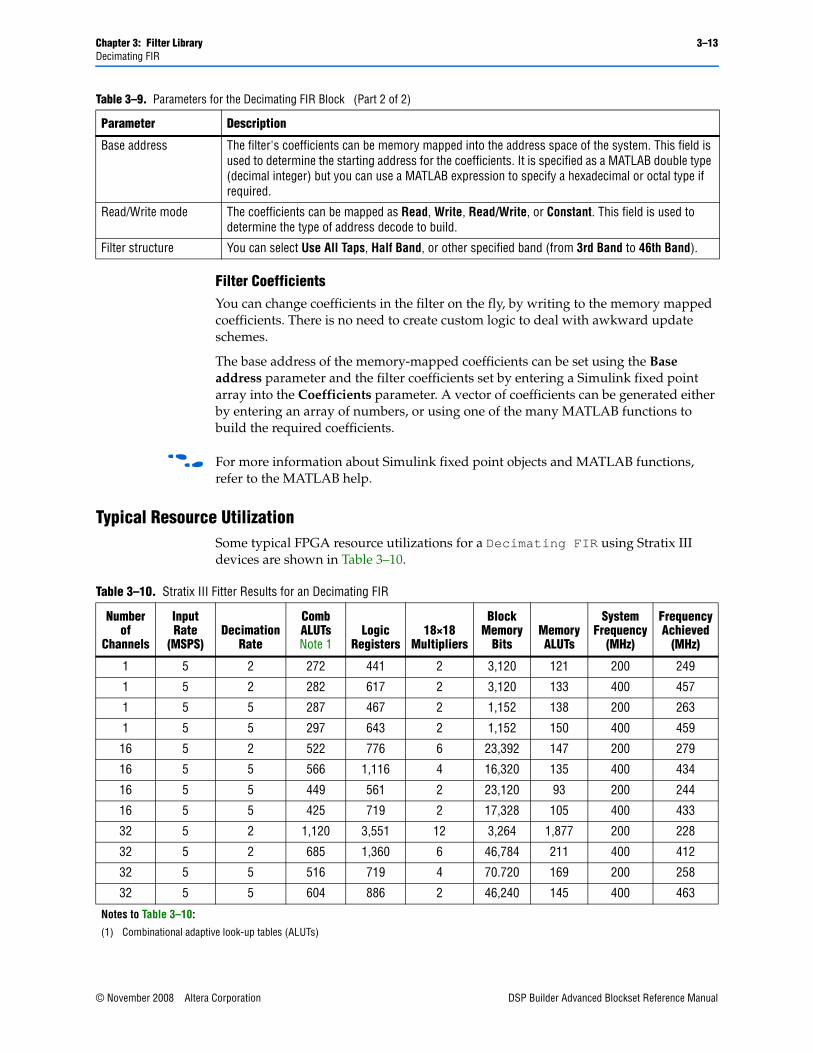
Typical Resource UtilizationSome typical FPGA resource utilizations for a Decimating FIR using Stratix III devices are shown in Table 3–10.
Base address The filter's coefficients can be memory mapped into the address space of the system. This field is used to determine the starting address for the coefficients. It is specified as a MATLAB double type (decimal integer) but you can use a MATLAB expression to specify a hexadecimal or octal type if required.
Read/Write mode The coefficients can be mapped as Read, Write, Read/Write, or Constant. This field is used to determine the type of address decode to build.
Filter structure You can select Use All Taps, Half Band, or other specified band (from 3rd Band to 46th Band).
Table 3–9. Parameters for the Decimating FIR Block (Part 2 of 2)
Parameter Description
Table 3–10. Stratix III Fitter Results for an Decimating FIR
Number of
Channels
Input Rate
(MSPS)Decimation
Rate
Comb ALUTs Note 1
Logic Registers
18×18 Multipliers
Block Memory
BitsMemory ALUTs
System Frequency
(MHz)
Frequency Achieved
(MHz)
1 5 2 272 441 2 3,120 121 200 249
1 5 2 282 617 2 3,120 133 400 457
1 5 5 287 467 2 1,152 138 200 263
1 5 5 297 643 2 1,152 150 400 459
16 5 2 522 776 6 23,392 147 200 279
16 5 5 566 1,116 4 16,320 135 400 434
16 5 5 449 561 2 23,120 93 200 244
16 5 5 425 719 2 17,328 105 400 433
32 5 2 1,120 3,551 12 3,264 1,877 200 228
32 5 2 685 1,360 6 46,784 211 400 412
32 5 5 516 719 4 70.720 169 200 258
32 5 5 604 886 2 46,240 145 400 463
Notes to Table 3–10:
(1) Combinational adaptive look-up tables (ALUTs)
© November 2008 Altera Corporation DSP Builder Advanced Blockset Reference Manual
3–14 Chapter 3: Filter LibraryDecimating FIR
Port InterfaceTable 3–11 shows the port interface for the Decimating FIR block.
Information MessagesWhenever the model runs within Simulink, messages are issued that are specific to the Decimating FIR block. For example, the amount of folding achieved per phase is reported. Some examples are shown in Table 3–12.
Table 3–11. Port Interface for the Decimating FIR Block
Signal Direction Description
a input The data input to the block. If more channels are requested than can fit on a single bus, this signal is a vector. The bit width is inherited from the input wire.
v input Indicates validity of the data input signals. If v is high, the data on the a wire is valid.
c input Indicates channel of data input signals. If v is high, then c indicates which channel the data corresponds to.
q output The data output from the block. If more channels are requested than can fit on a single bus, this signal is a vector. The bit width is a function of the input bit width and the parameterization.
v output Indicates validity of data output signals. Note 1
c output Indicates channel of data output signals. Note 1
Notes to Table 3–11:
(1) The output data can be non-zero when v is low.
Table 3–12. Messages for the Decimating FIR Block (Part 1 of 2)
Message Example Description
Written on Tue Feb 19 11:35:41 2008 Date and time when this file was run.
Decimating Filter Version: $Revision: 1.111 $
The version number and revision for the Decimating FIR Filter (Version 1, revision 111 in this example).
Number of physical input buses: 1 Depending on the input data rate, the number of wires needed to carry the input data may be more than 1. If so, the comb sections of the filter are duplicated (vectorized) to satisfy the data rate requirement.
Number of physical output buses: 2 Depending on the output data rate, the number of data wires needed to carry the output data may be more than 1. If so, the output wires are duplicated (vectorized) to satisfy the data rate requirement. The output data rate is the product of the input rate and the interpolation rate.
Calculated bit width of output stage: 26 This is the bit width of the (vectorized) data output from the filter.
Number of different phases: 1 The number of different phases.
Implementation Folding: 3 The number of times that each multiplier is used per sample to reduce the implementation size.
Filter Utilization: 48/50 (96.00%) For some sample rates, it is necessary to stall the filter internally for a number of cycles. The number of cycles used for active calculation is shown with the number of cycles determined by the sample rate relative to the system clock frequency.
Tap Utilization: 25/27 (92.59%) When some filters are folded there may be unused extra taps. The extra taps may be used to increase the filter length with no hardware resource increase.
Latency is 9 The latency introduced by this block.
DSP Builder Advanced Blockset Reference Manual © November 2008 Altera Corporation
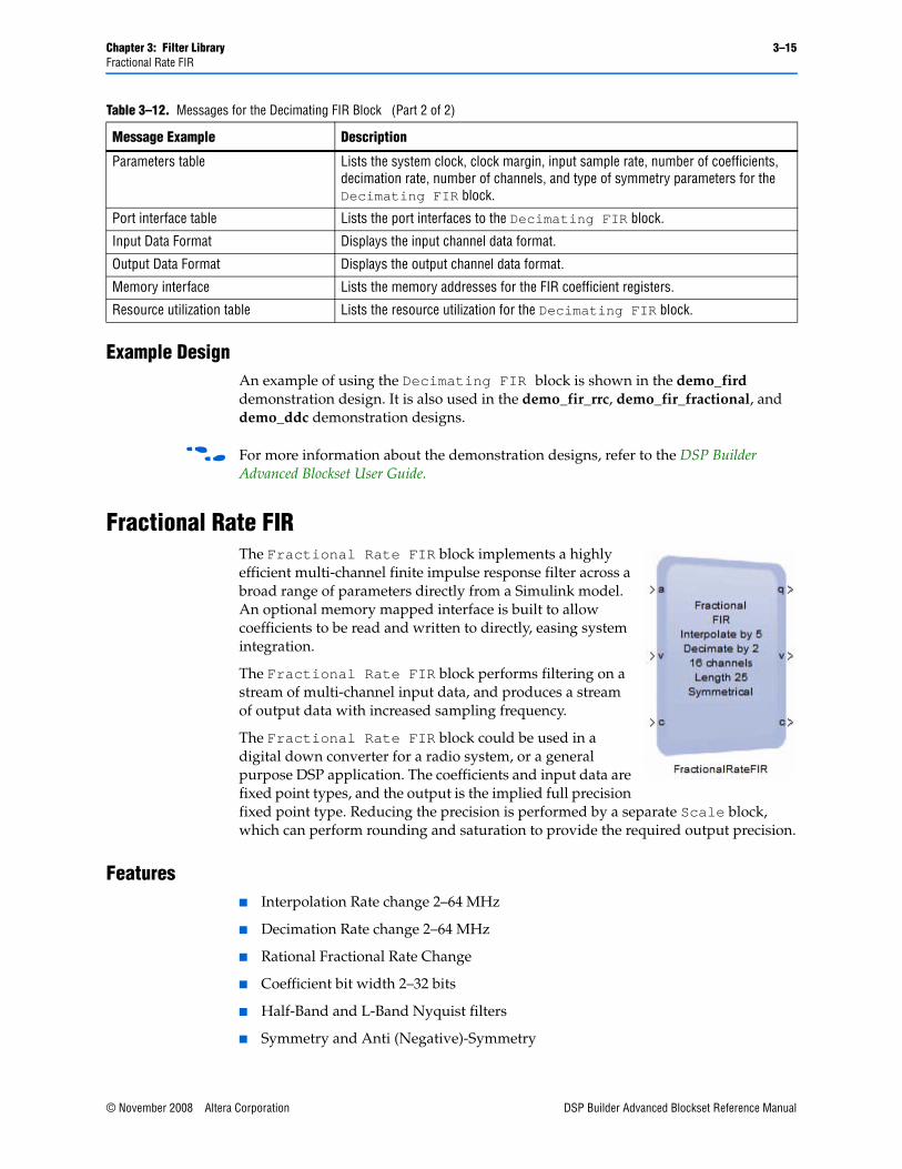
Chapter 3: Filter Library 3–15Fractional Rate FIR
Example DesignAn example of using the Decimating FIR block is shown in the demo_fird demonstration design. It is also used in the demo_fir_rrc, demo_fir_fractional, and demo_ddc demonstration designs.
f For more information about the demonstration designs, refer to the DSP Builder Advanced Blockset User Guide.
Fractional Rate FIRThe Fractional Rate FIR block implements a highly efficient multi-channel finite impulse response filter across a broad range of parameters directly from a Simulink model. An optional memory mapped interface is built to allow coefficients to be read and written to directly, easing system integration.
The Fractional Rate FIR block performs filtering on a stream of multi-channel input data, and produces a stream of output data with increased sampling frequency.
The Fractional Rate FIR block could be used in a digital down converter for a radio system, or a general purpose DSP application. The coefficients and input data are fixed point types, and the output is the implied full precision fixed point type. Reducing the precision is performed by a separate Scale block, which can perform rounding and saturation to provide the required output precision.
Features■ Interpolation Rate change 2–64 MHz
■ Decimation Rate change 2–64 MHz
■ Rational Fractional Rate Change
■ Coefficient bit width 2–32 bits
■ Half-Band and L-Band Nyquist filters
■ Symmetry and Anti (Negative)-Symmetry
Parameters table Lists the system clock, clock margin, input sample rate, number of coefficients, decimation rate, number of channels, and type of symmetry parameters for the Decimating FIR block.
Port interface table Lists the port interfaces to the Decimating FIR block.
Input Data Format Displays the input channel data format.
Output Data Format Displays the output channel data format.
Memory interface Lists the memory addresses for the FIR coefficient registers.
Resource utilization table Lists the resource utilization for the Decimating FIR block.
Table 3–12. Messages for the Decimating FIR Block (Part 2 of 2)
Message Example Description
© November 2008 Altera Corporation DSP Builder Advanced Blockset Reference Manual
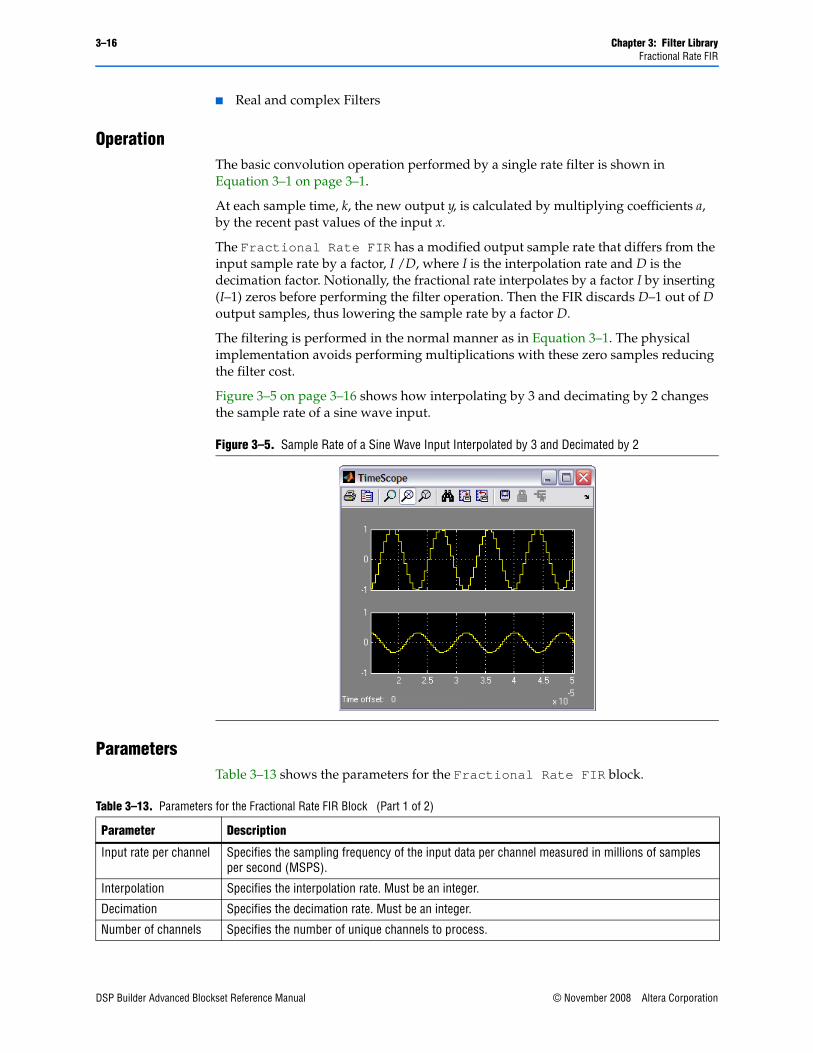
3–16 Chapter 3: Filter LibraryFractional Rate FIR
■ Real and complex Filters
OperationThe basic convolution operation performed by a single rate filter is shown in Equation 3–1 on page 3–1.
At each sample time, k, the new output y, is calculated by multiplying coefficients a, by the recent past values of the input x.
The Fractional Rate FIR has a modified output sample rate that differs from the input sample rate by a factor, I /D, where I is the interpolation rate and D is the decimation factor. Notionally, the fractional rate interpolates by a factor I by inserting (I–1) zeros before performing the filter operation. Then the FIR discards D–1 out of D output samples, thus lowering the sample rate by a factor D.
The filtering is performed in the normal manner as in Equation 3–1. The physical implementation avoids performing multiplications with these zero samples reducing the filter cost.
Figure 3–5 on page 3–16 shows how interpolating by 3 and decimating by 2 changes the sample rate of a sine wave input.
ParametersTable 3–13 shows the parameters for the Fractional Rate FIR block.
Figure 3–5. Sample Rate of a Sine Wave Input Interpolated by 3 and Decimated by 2
Table 3–13. Parameters for the Fractional Rate FIR Block (Part 1 of 2)
Parameter Description
Input rate per channel Specifies the sampling frequency of the input data per channel measured in millions of samples per second (MSPS).
Interpolation Specifies the interpolation rate. Must be an integer.
Decimation Specifies the decimation rate. Must be an integer.
Number of channels Specifies the number of unique channels to process.
DSP Builder Advanced Blockset Reference Manual © November 2008 Altera Corporation
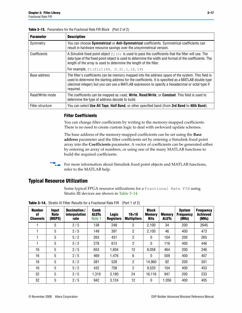
Chapter 3: Filter Library 3–17Fractional Rate FIR
Filter CoefficientsYou can change filter coefficients by writing to the memory-mapped coefficients. There is no need to create custom logic to deal with awkward update schemes.
The base address of the memory-mapped coefficients can be set using the Base address parameter and the filter coefficients set by entering a Simulink fixed point array into the Coefficients parameter. A vector of coefficients can be generated either by entering an array of numbers, or using one of the many MATLAB functions to build the required coefficients.
f For more information about Simulink fixed point objects and MATLAB functions, refer to the MATLAB help.
Typical Resource UtilizationSome typical FPGA resource utilizations for a Fractional Rate FIR using Stratix III devices are shown in Table 3–14.
Symmetry You can choose Symmetrical or Anti-Symmetrical coefficients. Symmetrical coefficients can result in hardware resource savings over the unsymmetrical version.
Coefficients A Simulink fixed point object fi(0) is used to pass the coefficients that the filter will use. The data type of the fixed point object is used to determine the width and format of the coefficients. The length of the array is used to determine the length of the filter.
For example, fi(fir1(49, 0.3),1,18,19)
Base address The filter's coefficients can be memory mapped into the address space of the system. This field is used to determine the starting address for the coefficients. It is specified as a MATLAB double type (decimal integer) but you can use a MATLAB expression to specify a hexadecimal or octal type if required.
Read/Write mode The coefficients can be mapped as Read, Write, Read/Write, or Constant. This field is used to determine the type of address decode to build.
Filter structure You can select Use All Taps, Half Band, or other specified band (from 3rd Band to 46th Band).
Table 3–13. Parameters for the Fractional Rate FIR Block (Part 2 of 2)
Parameter Description
Table 3–14. Stratix III Fitter Results for a Fractional Rate FIR (Part 1 of 2)
Number of
Channels
Input Rate
(MSPS)
Decimation / interpolation
rate
Comb ALUTs Note 1
Logic Registers
18×18 Multipliers
Block Memory
BitsMemory ALUTs
System Frequency
(MHz)
Frequency Achieved
(MHz)
1 5 2 / 5 138 248 2 2,100 34 200 2645
1 5 2 / 5 149 397 2 2,100 46 400 473
1 5 5 / 2 263 431 2 0 104 200 265
1 5 5 / 2 278 613 2 0 116 400 446
16 5 2 / 5 653 1,604 12 8,058 464 200 246
16 5 2 / 5 469 1,476 6 0 509 400 407
16 5 5 / 2 381 528 2 14,960 92 200 301
16 5 5 / 2 432 708 2 9,520 104 400 453
32 5 2 / 5 1,319 3,180 24 16,116 947 200 233
32 5 2 / 5 942 3,124 12 0 1,056 400 405
© November 2008 Altera Corporation DSP Builder Advanced Blockset Reference Manual
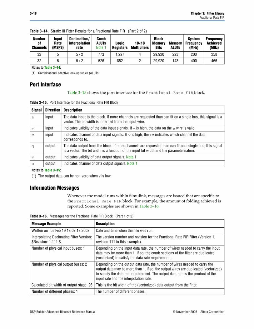
3–18 Chapter 3: Filter LibraryFractional Rate FIR
Port InterfaceTable 3–15 shows the port interface for the Fractional Rate FIR block.
Information MessagesWhenever the model runs within Simulink, messages are issued that are specific to the Fractional Rate FIR block. For example, the amount of folding achieved is reported. Some examples are shown in Table 3–16.
32 5 5 / 2 773 1,227 4 29,920 223 200 258
32 5 5 / 2 526 852 2 29,920 143 400 466
Notes to Table 3–14:
(1) Combinational adaptive look-up tables (ALUTs)
Table 3–14. Stratix III Fitter Results for a Fractional Rate FIR (Part 2 of 2)
Number of
Channels
Input Rate
(MSPS)
Decimation / interpolation
rate
Comb ALUTs Note 1
Logic Registers
18×18 Multipliers
Block Memory
BitsMemory ALUTs
System Frequency
(MHz)
Frequency Achieved
(MHz)
Table 3–15. Port Interface for the Fractional Rate FIR Block
Signal Direction Description
a input The data input to the block. If more channels are requested than can fit on a single bus, this signal is a vector. The bit width is inherited from the input wire.
v input Indicates validity of the data input signals. If v is high, the data on the a wire is valid.
c input Indicates channel of data input signals. If v is high, then c indicates which channel the data corresponds to.
q output The data output from the block. If more channels are requested than can fit on a single bus, this signal is a vector. The bit width is a function of the input bit width and the parameterization.
v output Indicates validity of data output signals. Note 1
c output Indicates channel of data output signals. Note 1
Notes to Table 3–15:
(1) The output data can be non-zero when v is low.
Table 3–16. Messages for the Fractional Rate FIR Block (Part 1 of 2)
Message Example Description
Written on Tue Feb 19 13:07:18 2008 Date and time when this file was run.
Interpolating Decimating Filter Version: $Revision: 1.111 $
The version number and revision for the Fractional Rate FIR Filter (Version 1, revision 111 in this example).
Number of physical input buses: 1 Depending on the input data rate, the number of wires needed to carry the input data may be more than 1. If so, the comb sections of the filter are duplicated (vectorized) to satisfy the data rate requirement.
Number of physical output buses: 2 Depending on the output data rate, the number of wires needed to carry the output data may be more than 1. If so, the output wires are duplicated (vectorized) to satisfy the data rate requirement. The output data rate is the product of the input rate and the interpolation rate.
Calculated bit width of output stage: 26 This is the bit width of the (vectorized) data output from the filter.
Number of different phases: 1 The number of different phases.
DSP Builder Advanced Blockset Reference Manual © November 2008 Altera Corporation

Chapter 3: Filter Library 3–19Interpolating CIC
Example DesignAn example of using the Fractional Rate FIR block is shown in the demo_firf, and demo_filters_flow_control demonstration designs.
f For more information about the demonstration designs, refer to the DSP Builder Advanced Blockset User Guide.
Interpolating CICThe Interpolating CIC block implements a highly efficient multi-channel cascaded integrator-comb filter across a broad range of parameters directly from a Simulink model.
The Interpolating CIC block performs filtering on a stream of multi-channel input data, and produces a stream of output data with increased sampling frequency.
The Interpolating CIC block could be used in a digital up converter for a radio system, or a general purpose DSP application. The coefficients and input data are fixed point types, and the output is the implied full precision fixed point type. Reducing the precision is performed by a separate Scale block, which can perform rounding and saturation to provide the required output precision.
Features■ Rate change 2–64 MHz
Implementation Folding: 3 The number of times that each multiplier is used per sample to reduce the implementation size.
Filter Utilization: 48/50 (96.00%) For some sample rates, it is necessary to stall the filter internally for a number of cycles. The number of cycles used for active calculation is shown with the number of cycles determined by the sample rate relative to the system clock frequency.
Tap Utilization: 25/27 (92.59%) When some filters are folded there may be unused extra taps. The extra taps may be used to increase the filter length with no hardware resource increase.
Latency is 9 The latency introduced by this block.
Parameters table Lists the system clock, clock margin, input sample rate, number of coefficients, interpolation rate, decimation rate, number of channels, and type of symmetry parameters for the Fractional Rate FIR block.
Port interface table Lists the port interfaces to the Fractional Rate FIR block.
Input Data Format Displays the input channel data format.
Output Data Format Displays the output channel data format.
Memory interface Lists the memory addresses for the FIR coefficient registers.
Resource utilization table Lists the resource utilization for the Fractional Rate FIR block.
Table 3–16. Messages for the Fractional Rate FIR Block (Part 2 of 2)
Message Example Description
© November 2008 Altera Corporation DSP Builder Advanced Blockset Reference Manual

3–20 Chapter 3: Filter LibraryInterpolating CIC
OperationThe Interpolating CIC has a higher output sample rate than the input sample rate by a factor I, where I is the interpolation rate. Notionally, the Interpolating CIC inserts (I–1) zeros for every input sample thus raising the sample rate by a factor I.
Figure 3–6 shows how interpolating by 5 increases the sample rate of a sine wave input.
ParametersTable 3–17 shows the parameters for the Interpolating CIC block.
Figure 3–6. Interpolate by 5 Filter Increasing Sample Rate of a Sine Wave Input
Table 3–17. Parameters for the Interpolating CIC Block
Parameter Description
Input rate per channel Specifies the sampling frequency of the input data per channel measured in millions of samples per second (MSPS).
Number of channels Specifies the number of unique channels to process.
Number of stages Specifies the number of comb and integrator stages.
Interpolation factor Specifies the interpolation factor. Must be an integer.
Differential delay Specifies the differential delay.
Final decimation You can optionally specify a final decimation by 2 to allow interpolation rates which are multiples of 0.5. The decimation works by simply throwing away data value. This option can only be used to reduce the number of unique outputs the CIC generates.
DSP Builder Advanced Blockset Reference Manual © November 2008 Altera Corporation
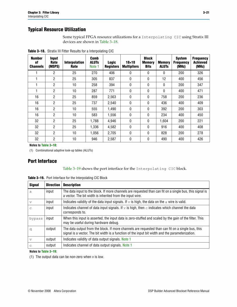
Chapter 3: Filter Library 3–21Interpolating CIC
Typical Resource UtilizationSome typical FPGA resource utilizations for a Interpolating CIC using Stratix III devices are shown in Table 3–18.
Port InterfaceTable 3–19 shows the port interface for the Interpolating CIC block.
Table 3–18. Stratix III Fitter Results for a Interpolating CIC
Number of
Channels
Input Rate
(MSPS)Interpolation
Rate
Comb ALUTs Note 1
Logic Registers
18×18 Multipliers
Block Memory
BitsMemory ALUTs
System Frequency
(MHz)
Frequency Achieved
(MHz)
1 2 25 270 406 0 0 0 200 326
1 2 25 305 837 0 0 12 400 456
1 2 10 258 394 0 0 0 200 347
1 2 10 287 771 0 0 0 400 471
16 2 25 859 2,563 0 0 758 200 236
16 2 25 737 2,540 0 0 436 400 409
16 2 10 555 1,490 0 0 392 200 303
16 2 10 583 1,556 0 0 234 400 450
32 2 25 1,788 4,946 0 0 1,604 200 221
32 2 25 1,336 4,582 0 0 916 400 408
32 2 10 1,056 2,705 0 0 828 200 278
32 2 10 946 2,587 0 0 490 400 426
Notes to Table 3–18:
(1) Combinational adaptive look-up tables (ALUTs)
Table 3–19. Port Interface for the Interpolating CIC Block
Signal Direction Description
a input The data input to the block. If more channels are requested than can fit on a single bus, this signal is a vector. The bit width is inherited from the input wire.
v input Indicates validity of the data input signals. If v is high, the data on the a wire is valid.
c input Indicates channel of data input signals. If v is high, then c indicates which channel the data corresponds to.
bypass input When this input is asserted, the input data is zero-stuffed and scaled by the gain of the filter. This may be useful during hardware debug.
q output The data output from the block. If more channels are requested than can fit on a single bus, this signal is a vector. The bit width is a function of the input bit width and the parameterization.
v output Indicates validity of data output signals. Note 1
c output Indicates channel of data output signals. Note 1
Notes to Table 3–19:
(1) The output data can be non-zero when v is low.
© November 2008 Altera Corporation DSP Builder Advanced Blockset Reference Manual
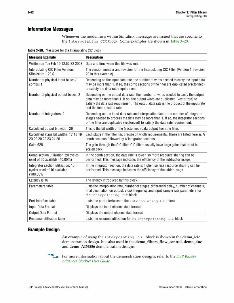
3–22 Chapter 3: Filter LibraryInterpolating CIC
Information MessagesWhenever the model runs within Simulink, messages are issued that are specific to the Interpolating CIC block. Some examples are shown in Table 3–20.
Example DesignAn example of using the Interpolating CIC block is shown in the demo_icic demonstration design. It is also used in the demo_filters_flow_control, demo_duc and demo_AD9856 demonstration designs.
f For more information about the demonstration designs, refer to the DSP Builder Advanced Blockset User Guide.
Table 3–20. Messages for the Interpolating CIC Block
Message Example Description
Written on Tue Feb 19 12:52:32 2008 Date and time when this file was run.
Interpolating CIC Filter Version: $Revision: 1.20 $
The version number and revision for the Interpolating CIC Filter (Version 1, revision 20 in this example).
Number of physical input buses / combs: 1
Depending on the input data rate, the number of wires needed to carry the input data may be more than 1. If so, the comb sections of the filter are duplicated (vectorized) to satisfy the data rate requirement.
Number of physical output buses: 2 Depending on the output data rate, the number of wires needed to carry the output data may be more than 1. If so, the output wires are duplicated (vectorized) to satisfy the data rate requirement. The output data rate is the product of the input rate and the interpolation rate.
Number of integrators: 2 Depending on the input data rate and interpolation factor the number of integrator stages needed to process the data may be more than 1. If so, the integrator sections of the filter are duplicated (vectorized) to satisfy the data rate requirement.
Calculated output bit width: 26 This is the bit width of the (vectorized) data output from the filter.
Calculated stage bit widths: 17 18 19 20 20 20 22 23 24 26
Each stage in the filter has precise bit width requirements. These are listed here as N comb sections followed by N integrator sections.
Gain: 625 The gain through the CIC filter. CIC filters usually have large gains that must be scaled back.
Comb section utilization: 20 cycles used of 50 available (40.00%)
In the comb section, the data rate is lower, so more resource sharing can be performed. This message indicates the efficiency of the subtractor usage.
Integrator section utilization: 10 cycles used of 10 available (100.00%)
In the integrator section, the data rate is higher, so less resource sharing can be performed. This message indicates the efficiency of the adder usage.
Latency is 16 The latency introduced by this block.
Parameters table Lists the interpolation rate, number of stages, differential delay, number of channels, final decimation on output, clock frequency and input sample rate parameters for the Interpolating CIC block.
Port interface table Lists the port interfaces to the Interpolating CIC block.
Input Data Format Displays the input channel data format.
Output Data Format Displays the output channel data format.
Resource utilization table Lists the resource utilization for the Interpolating CIC block.
DSP Builder Advanced Blockset Reference Manual © November 2008 Altera Corporation
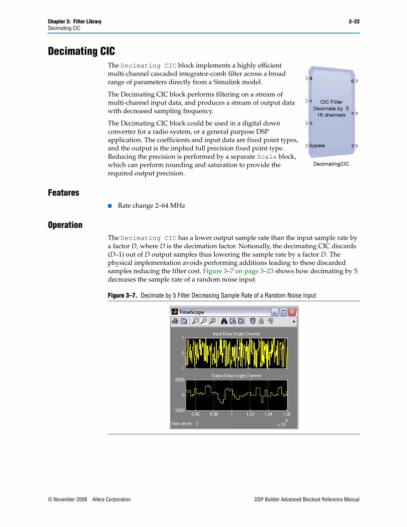
Chapter 3: Filter Library 3–23Decimating CIC
Decimating CICThe Decimating CIC block implements a highly efficient multi-channel cascaded integrator-comb filter across a broad range of parameters directly from a Simulink model.
The Decimating CIC block performs filtering on a stream of multi-channel input data, and produces a stream of output data with decreased sampling frequency.
The Decimating CIC block could be used in a digital down converter for a radio system, or a general purpose DSP application. The coefficients and input data are fixed point types, and the output is the implied full precision fixed point type. Reducing the precision is performed by a separate Scale block, which can perform rounding and saturation to provide the required output precision.
Features■ Rate change 2–64 MHz
OperationThe Decimating CIC has a lower output sample rate than the input sample rate by a factor D, where D is the decimation factor. Notionally, the decimating CIC discards (D–1) out of D output samples thus lowering the sample rate by a factor D. The physical implementation avoids performing additions leading to these discarded samples reducing the filter cost. Figure 3–7 on page 3–23 shows how decimating by 5 decreases the sample rate of a random noise input.
Figure 3–7. Decimate by 5 Filter Decreasing Sample Rate of a Random Noise Input
© November 2008 Altera Corporation DSP Builder Advanced Blockset Reference Manual
3–24 Chapter 3: Filter LibraryDecimating CIC
ParametersTable 3–21 shows the parameters for the Decimating CIC block.
Typical Resource UtilizationSome typical FPGA resource utilizations for a Decimating CIC using Stratix III devices are shown in Table 3–22.
Port InterfaceTable 3–23 shows the port interface for the Decimating CIC block.
Table 3–21. Parameters for the Decimating CIC Block
Parameter Description
Input rate per channel Specifies the sampling frequency of the input data per channel measured in millions of samples per second (MSPS).
Number of channels Specifies the number of unique channels to process.
Number of stages Specifies the number of comb and integrator stages.
Decimation factor Specifies the decimation factor 1/(integer). (An integer greater than 1 implies interpolation.)
Differential delay Specifies the differential delay.
Table 3–22. Stratix III Fitter Results for a Decimating CIC
Number of
Channels
Input Rate
(MSPS)Decimation
Rate
Comb ALUTs Note 1
Logic Registers
18×18 Multipliers
Block Memory
BitsMemory ALUTs
System Frequency
(MHz)
Frequency Achieved
(MHz)
1 10 2 240 391 0 0 0 200 380
1 10 2 260- 487 0 0 0 400 469
1 10 10 363 585 0 0 0 200 278
1 10 10 403 857 0 0 0 400 462
16 10 2 403 946 0 0 230 200 340
16 10 2 472 1,149 0 0 230 400 419
16 10 10 526 1,320 0 0 350 200 261
16 10 10 664 1,806 0 0 350 400 443
132 10 2 812 1,612 0 0 478 200 275
32 10 2 819 1,433 0 0 460 400 430
32 10 10 1,055 2,226 0 0 718 200 259
32 10 10 1,159 2,226 0 0 700 400 416
Notes to Table 3–22:
(1) Combinational adaptive look-up tables (ALUTs)
Table 3–23. Port Interface for the Decimating CIC Block (Part 1 of 2)
Signal Direction Description
a input The data input to the block. If more channels are requested than can fit on a single bus, this signal is a vector. The bit width is inherited from the input wire.
v input Indicates validity of the data input signals. If v is high, the data on the a wire is valid.
DSP Builder Advanced Blockset Reference Manual © November 2008 Altera Corporation
Chapter 3: Filter Library 3–25Decimating CIC
Information MessagesWhenever the model runs within Simulink, messages are issued that are specific to the Decimating CIC block. Some examples are shown in Table 3–24.
c input Indicates channel of data input signals. If v is high, then c indicates which channel the data corresponds to.
bypass input When this input is asserted, the input data is zero-stuffed and scaled by the gain of the filter. This may be useful during hardware debug.
q output The data output from the block. If more channels are requested than can fit on a single bus, this signal is a vector. The bit width is a function of the input bit width and the parameterization.
v output Indicates validity of data output signals. Note 1
c output Indicates channel of data output signals. Note 1
Notes to Table 3–23:
(1) The output data can be non-zero when v is low.
Table 3–23. Port Interface for the Decimating CIC Block (Part 2 of 2)
Signal Direction Description
Table 3–24. Messages for the Decimating CIC Block (Part 1 of 2)
Message Example Description
Written on Tue Feb 19 11:25:27 2008 Date and time when this file was run.
Decimating CIC Filter Version: $Revision: 1.20 $
The version number and revision for the Decimating CIC Filter (Version 1, revision 20 in this example).
Number of physical input buses / integrators: 1
Depending on the input data rate, the number of wires needed to carry the input data may be more than 1. If so, the integrator sections of the filter are duplicated (vectorized) to satisfy the data rate requirement.
Number of physical output buses / combs: 2
Depending on the output data rate, the number of wires needed to carry the output data may be more than 1. If so, the output wires are duplicated (vectorized) to satisfy the data rate requirement. The output data rate is the product of the input rate and the interpolation rate.
Number of integrators: 2 Depending on the input data rate and interpolation factor the number of integrator stages needed to process the data may be more than 1. If so, the integrator sections of the filter are duplicated (vectorized) to satisfy the data rate requirement.
Calculated output bit width: 26 This is the bit width of the (vectorized) data output from the filter.
Calculated stage bit widths: 17 18 19 20 20 20 22 23 24 26
Each stage in the filter has precise bit width requirements. These are listed here as N comb sections followed by N integrator sections.
Gain: 625 The gain through the CIC filter. CIC filters usually have large gains that must be scaled back.
Comb section utilization: 20 cycles used of 50 available (40.00%)
In the comb section, the data rate is lower, so more resource sharing can be performed. This message indicates the efficiency of the subtractor usage.
Integrator section utilization: 10 cycles used of 10 available (100.00%)
In the integrator section, the data rate is higher, so less resource sharing can be performed. This message indicates the efficiency of the adder usage.
Latency is 13 The latency introduced by this block.
Parameters table Lists the decimation rate, number of stages, differential delay, number of channels, clock frequency and input sample rate parameters for the Decimating CIC block.
© November 2008 Altera Corporation DSP Builder Advanced Blockset Reference Manual
3–26 Chapter 3: Filter LibraryDecimating CIC
Example DesignAn example of using the Decimating CIC block is shown in the demo_dcic demonstration design. It is also used in the demo_ddc demonstration design.
f For more information about the demonstration designs, refer to the DSP Builder Advanced Blockset User Guide.
Port interface table Lists the port interfaces to the Decimating CIC block.
Input Data Format Displays the input channel data format.
Output Data Format Displays the output channel data format.
Resource utilization table Lists the resource utilization for the Decimating CIC block.
Table 3–24. Messages for the Decimating CIC Block (Part 2 of 2)
Message Example Description
DSP Builder Advanced Blockset Reference Manual © November 2008 Altera Corporation

© November 2008 Altera Corporation
4. FFT Library
The FFT Library contains the following blocks in the Common folder:
Complex Multiplier (ComplexMult). . . . . . . . . . . . . . . . . . . . . . . . . . . . . . . . . . . . . . 4–2Complex Sample Delay. . . . . . . . . . . . . . . . . . . . . . . . . . . . . . . . . . . . . . . . . . . . . . . . . 4–3Dual Twiddle Memory . . . . . . . . . . . . . . . . . . . . . . . . . . . . . . . . . . . . . . . . . . . . . . . . . 4–5Negate . . . . . . . . . . . . . . . . . . . . . . . . . . . . . . . . . . . . . . . . . . . . . . . . . . . . . . . . . . . . . . . 4–6Negate Parameterizable . . . . . . . . . . . . . . . . . . . . . . . . . . . . . . . . . . . . . . . . . . . . . . . . 4–6
The following blocks are available in the Radix2 folder:
Butterfly I (BFI). . . . . . . . . . . . . . . . . . . . . . . . . . . . . . . . . . . . . . . . . . . . . . . . . . . . . . . . 4–7Butterfly II (BFII) . . . . . . . . . . . . . . . . . . . . . . . . . . . . . . . . . . . . . . . . . . . . . . . . . . . . . . 4–8Bit Reverse Core . . . . . . . . . . . . . . . . . . . . . . . . . . . . . . . . . . . . . . . . . . . . . . . . . . . . . . 4–10Twiddle Generator. . . . . . . . . . . . . . . . . . . . . . . . . . . . . . . . . . . . . . . . . . . . . . . . . . . . 4–11
1 The blocks in the Radix 2 folder support a hardware oriented Radix-22 algorithm based on a twiddle factor decomposition technique using butterfly structures.
f For more information about the Radix-22 algorithm, refer to A New Approach to Pipeline FFT Processor – Shousheng He & Mats Torkleson, Department of Applied Electronics, Lund University, Sweden.
DSP Builder Advanced Blockset Reference Manual
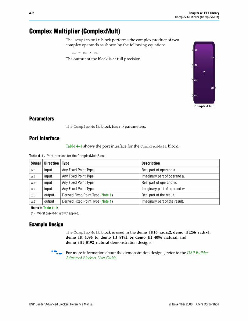
4–2 Chapter 4: FFT LibraryComplex Multiplier (ComplexMult)
Complex Multiplier (ComplexMult)The ComplexMult block performs the complex product of two complex operands as shown by the following equation:
zr = ar × wr
The output of the block is at full precision.
ParametersThe ComplexMult block has no parameters.
Port InterfaceTable 4–1 shows the port interface for the ComplexMult block.
Example DesignThe ComplexMult block is used in the demo_fft16_radix2, demo_fft256_radix4, demo_fft_4096_br, demo_fft_8192_br, demo_fft_4096_natural, and demo_ifft_8192_natural demonstration designs.
f For more information about the demonstration designs, refer to the DSP Builder Advanced Blockset User Guide.
Table 4–1. Port Interface for the ComplexMult Block
Signal Direction Type Description
ar input Any Fixed Point Type Real part of operand a.
ai input Any Fixed Point Type Imaginary part of operand a.
wr input Any Fixed Point Type Real part of operand w.
wi input Any Fixed Point Type Imaginary part of operand w.
zr output Derived Fixed Point Type (Note 1) Real part of the result.
zi output Derived Fixed Point Type (Note 1) Imaginary part of the result.
Notes to Table 4–1:
(1) Worst case 8-bit growth applied.
DSP Builder Advanced Blockset Reference Manual © November 2008 Altera Corporation

Chapter 4: FFT Library 4–3Complex Sample Delay
Complex Sample DelayThe Complex Sample Delay block applies a fixed delay Z to the incoming complex data stream as shown by the equations:
Out1 = In1 × (1/Z)Out2 = In2 × (1/Z)
The block conveniently accepts two samples to support complex data streams, and is typically used in fully streaming FFT architectures. A single synthesis time parameter is used to configure the length of the delay.
The output type of this block is normally inherited (using an internal rule) and the type propagates through the design automatically. However, if the block is used in a loop, it is necessary to specify the output type for at least one block in the loop. This can be done by performing the following steps:
1. Click on the Complex Sample Delay block with the right mouse button and select Look Under Mask to reveal that the block is implemented by two primitive Sample Delay blocks:
2. Double click on each Sample Delay block and set the output data type mode using the parameters described for “Sample Delay” on page 7–34. You are warned that you are attempting to change the parameters of a library block. Click OK to confirm this dialog box.
ParametersTable 4–2 shows the parameters for the Complex Sample Delay block.
Port InterfaceTable 4–3 shows the port interface for the Complex Sample Delay block.
Table 4–2. Parameters for the Complex Sample Delay Block
Parameter Description
Delay Specifies the delay.
Table 4–3. Port Interface for the Complex Sample Delay Block
Signal Direction Type Description
In1 input Inherited Fixed Point Type Data input 1
In2 input Inherited Fixed Point Type Data input 2
© November 2008 Altera Corporation DSP Builder Advanced Blockset Reference Manual
4–4 Chapter 4: FFT LibraryComplex Sample Delay
Example DesignThe Complex Sample Delay block is used in the demo_fft16_radix2, demo_fft256_radix4, demo_fft_4096_br, demo_fft_8192_br, demo_fft_4096_natural, and demo_ifft_8192_natural demonstration designs.
f For more information about the demonstration designs, refer to the DSP Builder Advanced Blockset User Guide.
Out1 output Inherited Fixed Point Type (same as In1) Data output 1
Out2 output Inherited Fixed Point Type (same as In2) Data output 2
Table 4–3. Port Interface for the Complex Sample Delay Block
Signal Direction Type Description
DSP Builder Advanced Blockset Reference Manual © November 2008 Altera Corporation
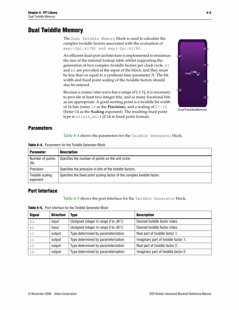
Chapter 4: FFT Library 4–5Dual Twiddle Memory
Dual Twiddle MemoryThe Dual Twiddle Memory block is used to calculate the complex twiddle factors associated with the evaluation of exp(-2pi.k1/N) and exp(-2pi.k2/N).
An efficient dual-port architecture is implemented to minimize the size of the internal lookup table whilst supporting the generation of two complex twiddle factors per clock cycle. k1 and k2 are provided at the input of the block, and they must be less than or equal to a synthesis time parameter N. The bit width and fixed point scaling of the twiddle factors should also be entered.
Because a cosine/sine wave has a range of [-1:1], it is necessary to provide at least two integer bits, and as many fractional bits as are appropriate. A good starting point is a twiddle bit width of 16 bits (enter 16 as the Precision), and a scaling of 2^-14 (Enter 14 as the Scaling exponent). The resulting fixed point type is sfix16_en14 (2.14 in fixed point format).
ParametersTable 4–4 shows the parameters for the Twiddle Generator block.
Port InterfaceTable 4–5 shows the port interface for the Twiddle Generator block.
Table 4–4. Parameters for the Twiddle Generator Block
Parameter Description
Number of points (N)
Specifies the number of points on the unit circle.
Precision Specifies the precision in bits of the twiddle factors.
Twiddle scaling exponent
Specifies the fixed point scaling factor of the complex twiddle factor.
Table 4–5. Port Interface for the Twiddle Generator Block
Signal Direction Type Description
k1 input Unsigned integer in range 0 to (N-1) Desired twiddle factor index.
k2 input Unsigned integer in range 0 to (N-1) Desired twiddle factor index.
r1 output Type determined by parameterization Real part of twiddle factor 1.
i1 output Type determined by parameterization Imaginary part of twiddle factor 1.
r2 output Type determined by parameterization Real part of twiddle factor 2.
i2 output Type determined by parameterization Imaginary part of twiddle factor 2.
© November 2008 Altera Corporation DSP Builder Advanced Blockset Reference Manual
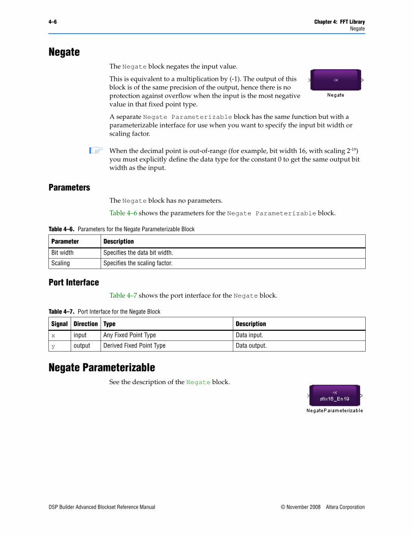
4–6 Chapter 4: FFT LibraryNegate
NegateThe Negate block negates the input value.
This is equivalent to a multiplication by (-1). The output of this block is of the same precision of the output, hence there is no protection against overflow when the input is the most negative value in that fixed point type.
A separate Negate Parameterizable block has the same function but with a parameterizable interface for use when you want to specify the input bit width or scaling factor.
1 When the decimal point is out-of-range (for example, bit width 16, with scaling 2-19) you must explicitly define the data type for the constant 0 to get the same output bit width as the input.
ParametersThe Negate block has no parameters.
Table 4–6 shows the parameters for the Negate Parameterizable block.
Port InterfaceTable 4–7 shows the port interface for the Negate block.
Negate ParameterizableSee the description of the Negate block.
Table 4–6. Parameters for the Negate Parameterizable Block
Parameter Description
Bit width Specifies the data bit width.
Scaling Specifies the scaling factor.
Table 4–7. Port Interface for the Negate Block
Signal Direction Type Description
x input Any Fixed Point Type Data input.
y output Derived Fixed Point Type Data output.
DSP Builder Advanced Blockset Reference Manual © November 2008 Altera Corporation
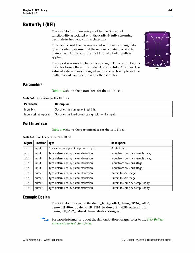
Chapter 4: FFT Library 4–7Butterfly I (BFI)
Butterfly I (BFI)The BFI block implements provides the Butterfly I functionality associated with the Radix-22 fully streaming decimate in frequency FFT architecture.
This block should be parameterized with the incoming data type in order to ensure that the necessary data precision is maintained. At the output, an additional bit of growth is applied.
The s port is connected to the control logic. This control logic is the extraction of the appropriate bit of a modulo N counter. The value of s determines the signal routing of each sample and the mathematical combination with other samples.
ParametersTable 4–8 shows the parameters for the BFI block.
Port InterfaceTable 4–9 shows the port interface for the BFI block.
Example DesignThe BFI block is used in the demo_fft16_radix2, demo_fft256_radix4, demo_fft_4096_br, demo_fft_8192_br, demo_fft_4096_natural, and demo_ifft_8192_natural demonstration designs.
f For more information about the demonstration designs, refer to the DSP Builder Advanced Blockset User Guide.
Table 4–8. Parameters for the BFI Block
Parameter Description
Input bits Specifies the number of input bits.
Input scaling exponent Specifies the fixed point scaling factor of the input.
Table 4–9. Port Interface for the BFI Block
Signal Direction Type Description
s input Boolean or unsigned integer uint(1) Control pin.
xr1 input Type determined by parameterization Input from complex sample delay.
xl1 input Type determined by parameterization Input from complex sample delay.
xr2 input Type determined by parameterization Input from previous stage.
xl2 input Type determined by parameterization Input from previous stage.
zr1 output Type determined by parameterization Output to next stage.
zl1 output Type determined by parameterization Output to next stage.
zr2 output Type determined by parameterization Output to complex sample delay.
zl2 output Type determined by parameterization Output to complex sample delay.
© November 2008 Altera Corporation DSP Builder Advanced Blockset Reference Manual
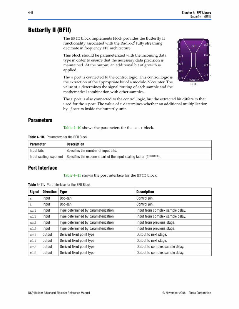
4–8 Chapter 4: FFT LibraryButterfly II (BFII)
Butterfly II (BFII)The BFII block implements block provides the Butterfly II functionality associated with the Radix-22 fully streaming decimate in frequency FFT architecture.
This block should be parameterized with the incoming data type in order to ensure that the necessary data precision is maintained. At the output, an additional bit of growth is applied.
The s port is connected to the control logic. This control logic is the extraction of the appropriate bit of a modulo N counter. The value of s determines the signal routing of each sample and the mathematical combination with other samples.
The t port is also connected to the control logic, but the extracted bit differs to that used for the s port. The value of t determines whether an additional multiplication by –j occurs inside the butterfly unit.
ParametersTable 4–10 shows the parameters for the BFII block.
Port InterfaceTable 4–11 shows the port interface for the BFII block.
Table 4–10. Parameters for the BFII Block
Parameter Description
Input bits Specifies the number of input bits.
Input scaling exponent Specifies the exponent part of the input scaling factor (2-exponent).
Table 4–11. Port Interface for the BFII Block
Signal Direction Type Description
s input Boolean Control pin.
t input Boolean Control pin.
xr1 input Type determined by parameterization Input from complex sample delay.
xl1 input Type determined by parameterization Input from complex sample delay.
xr2 input Type determined by parameterization Input from previous stage.
xl2 input Type determined by parameterization Input from previous stage.
zr1 output Derived fixed point type Output to next stage.
zl1 output Derived fixed point type Output to next stage.
zr2 output Derived fixed point type Output to complex sample delay.
zl2 output Derived fixed point type Output to complex sample delay.
DSP Builder Advanced Blockset Reference Manual © November 2008 Altera Corporation

Chapter 4: FFT Library 4–9Butterfly II (BFII)
Example DesignThe BFII block is used in the demo_fft256_radix4, demo_fft_4096_br, demo_fft_8192_br, demo_fft_4096_natural, and demo_ifft_8192_natural demonstration designs.
f For more information about the demonstration designs, refer to the DSP Builder Advanced Blockset User Guide.
© November 2008 Altera Corporation DSP Builder Advanced Blockset Reference Manual
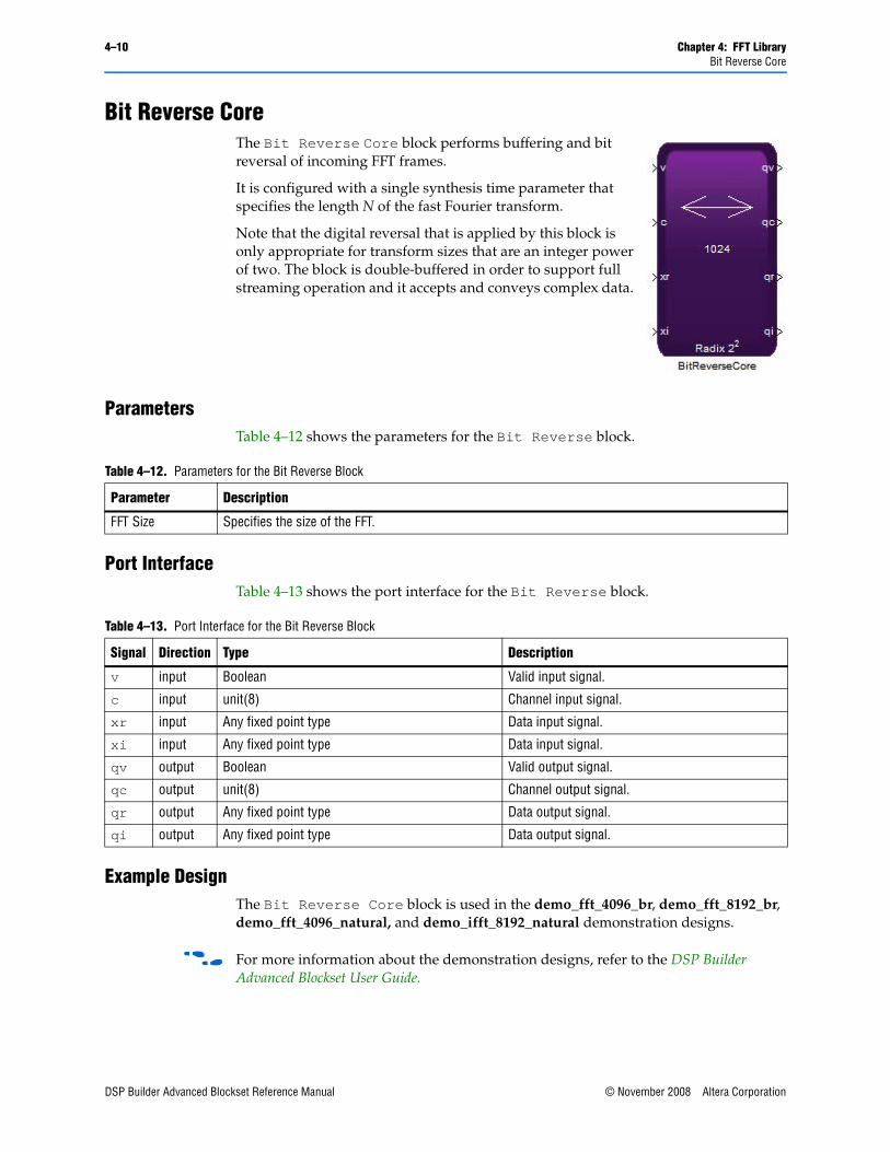
4–10 Chapter 4: FFT LibraryBit Reverse Core
Bit Reverse CoreThe Bit Reverse Core block performs buffering and bit reversal of incoming FFT frames.
It is configured with a single synthesis time parameter that specifies the length N of the fast Fourier transform.
Note that the digital reversal that is applied by this block is only appropriate for transform sizes that are an integer power of two. The block is double-buffered in order to support full streaming operation and it accepts and conveys complex data.
ParametersTable 4–12 shows the parameters for the Bit Reverse block.
Port InterfaceTable 4–13 shows the port interface for the Bit Reverse block.
Example DesignThe Bit Reverse Core block is used in the demo_fft_4096_br, demo_fft_8192_br, demo_fft_4096_natural, and demo_ifft_8192_natural demonstration designs.
f For more information about the demonstration designs, refer to the DSP Builder Advanced Blockset User Guide.
Table 4–12. Parameters for the Bit Reverse Block
Parameter Description
FFT Size Specifies the size of the FFT.
Table 4–13. Port Interface for the Bit Reverse Block
Signal Direction Type Description
v input Boolean Valid input signal.
c input unit(8) Channel input signal.
xr input Any fixed point type Data input signal.
xi input Any fixed point type Data input signal.
qv output Boolean Valid output signal.
qc output unit(8) Channel output signal.
qr output Any fixed point type Data output signal.
qi output Any fixed point type Data output signal.
DSP Builder Advanced Blockset Reference Manual © November 2008 Altera Corporation
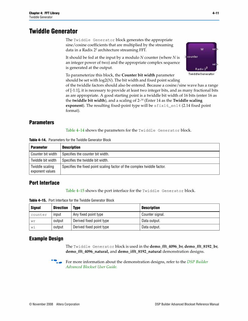
Chapter 4: FFT Library 4–11Twiddle Generator
Twiddle GeneratorThe Twiddle Generator block generates the appropriate sine/cosine coefficients that are multiplied by the streaming data in a Radix 22 architecture streaming FFT.
It should be fed at the input by a modulo N counter (where N is an integer power of two) and the appropriate complex sequence is generated at the output.
To parameterize this block, the Counter bit width parameter should be set with log2(N). The bit width and fixed point scaling of the twiddle factors should also be entered. Because a cosine/sine wave has a range of [-1:1], it is necessary to provide at least two integer bits, and as many fractional bits as are appropriate. A good starting point is a twiddle bit width of 16 bits (enter 16 as the twiddle bit width), and a scaling of 2-14 (Enter 14 as the Twiddle scaling exponent). The resulting fixed-point type will be sfix16_en14 (2.14 fixed point format).
ParametersTable 4–14 shows the parameters for the Twiddle Generator block.
Port InterfaceTable 4–15 shows the port interface for the Twiddle Generator block.
Example DesignThe Twiddle Generator block is used in the demo_fft_4096_br, demo_fft_8192_br, demo_fft_4096_natural, and demo_ifft_8192_natural demonstration designs.
f For more information about the demonstration designs, refer to the DSP Builder Advanced Blockset User Guide.
Table 4–14. Parameters for the Twiddle Generator Block
Parameter Description
Counter bit width Specifies the counter bit width.
Twiddle bit width Specifies the twiddle bit width.
Twiddle scaling exponent values
Specifies the fixed point scaling factor of the complex twiddle factor.
Table 4–15. Port Interface for the Twiddle Generator Block
Signal Direction Type Description
counter input Any fixed point type Counter signal.
wr output Derived fixed point type Data output.
wi output Derived fixed point type Data output.
© November 2008 Altera Corporation DSP Builder Advanced Blockset Reference Manual

4–12 Chapter 4: FFT LibraryTwiddle Generator
DSP Builder Advanced Blockset Reference Manual © November 2008 Altera Corporation
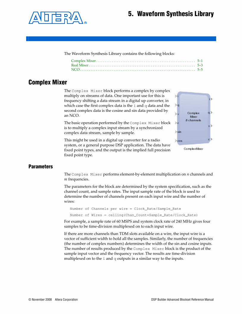
© November 2008 Altera Corporation
5. Waveform Synthesis Library
The Waveform Synthesis Library contains the following blocks:
Complex Mixer. . . . . . . . . . . . . . . . . . . . . . . . . . . . . . . . . . . . . . . . . . . . . . . . . . . . . . . . 5–1Real Mixer . . . . . . . . . . . . . . . . . . . . . . . . . . . . . . . . . . . . . . . . . . . . . . . . . . . . . . . . . . . . 5–3NCO . . . . . . . . . . . . . . . . . . . . . . . . . . . . . . . . . . . . . . . . . . . . . . . . . . . . . . . . . . . . . . . . . 5–5
Complex MixerThe Complex Mixer block performs a complex by complex multiply on streams of data. One important use for this is frequency shifting a data stream in a digital up converter, in which case the first complex data is the i and q data and the second complex data is the cosine and sin data provided by an NCO.
The basic operation performed by the Complex Mixer block is to multiply a complex input stream by a synchronized complex data stream, sample by sample.
This might be used in a digital up converter for a radio system, or a general purpose DSP application. The data have fixed point types, and the output is the implied full precision fixed point type.
ParametersThe Complex Mixer performs element-by-element multiplication on n channels and m frequencies.
The parameters for the block are determined by the system specification, such as the channel count, and sample rates. The input sample rate of the block is used to determine the number of channels present on each input wire and the number of wires:
Number of Channels per wire = Clock_Rate/Sample_Rate
Number of Wires = ceiling(Chan_Count×Sample_Rate/Clock_Rate)
For example, a sample rate of 60 MSPS and system clock rate of 240 MHz gives four samples to be time-division multiplexed on to each input wire.
If there are more channels than TDM slots available on a wire, the input wire is a vector of sufficient width to hold all the samples. Similarly, the number of frequencies (the number of complex numbers) determines the width of the sin and cosine inputs. The number of results produced by the Complex Mixer block is the product of the sample input vector and the frequency vector. The results are time-division multiplexed on to the i and q outputs in a similar way to the inputs.
DSP Builder Advanced Blockset Reference Manual
5–2 Chapter 5: Waveform Synthesis LibraryComplex Mixer
Table 5–1 shows the parameters for the Complex Mixer block.
Port InterfaceTable 5–2 shows the port interface for the Complex Mixer block.
Information MessagesTable 5–3 shows typical Help messages that can be issued for the Complex Mixer block.
Table 5–1. Parameters for the Complex Mixer Block
Parameter Description
Input Rate Per Channel (MSPS) The data rate per channel measured in millions of samples per second.
Number of Complex Channels The number of complex input channels.
Number of Frequencies The number of complex frequencies used in the multiplier.
Table 5–2. Port Interface for the Complex Mixer Block
Signal Direction Description
i input The real (in phase) half of the complex data input. If more channels are requested than can fit on a single bus, this signal is a vector. The bit width is inherited from the input wire.
q input The complex (quadrature phase) half of the complex data input. If more channels are requested than can fit on a single bus, this signal is a vector. The bit width is inherited from the input wire.
v input Indicates validity of data input signals. If v is high the data on the a wire is valid.
c input Indicates channel of data input signals. If v is high, then c indicates the data channel data.
sin input The imaginary part of the complex number. For example, the NCO's sine output for a quadrature mixer.
cos input The imaginary part of the complex number. For example, the NCO’s cosine output for a quadrature mixer.
i output The in phase (real) output of the mixer. This is (i × cos – q × sin). If more channels are requested than can fit on a single bus, this signal is a vector. The bit width is wide enough for the full precision result.
q output The quadrature phase (imaginary) output of the mixer. This is (i × sin + q × cos). If more channels are requested than can fit on a single bus, this signal is a vector. The bit width is wide enough for the full precision result.
v output Indicates validity of data output signals.
c output Indicates validity of data output signals.
Table 5–3. Messages for the Complex Mixer Block
Message Example Description
Written on Tue Feb 19 11:25:27 2008 Date and time when this file was run.
Latency is 4 The latency introduced by this block.
Port interface table Lists the port interfaces to the Complex Mixer block.
Resource utilization table Lists the resource utilization for the Complex Mixer block.
DSP Builder Advanced Blockset Reference Manual © November 2008 Altera Corporation
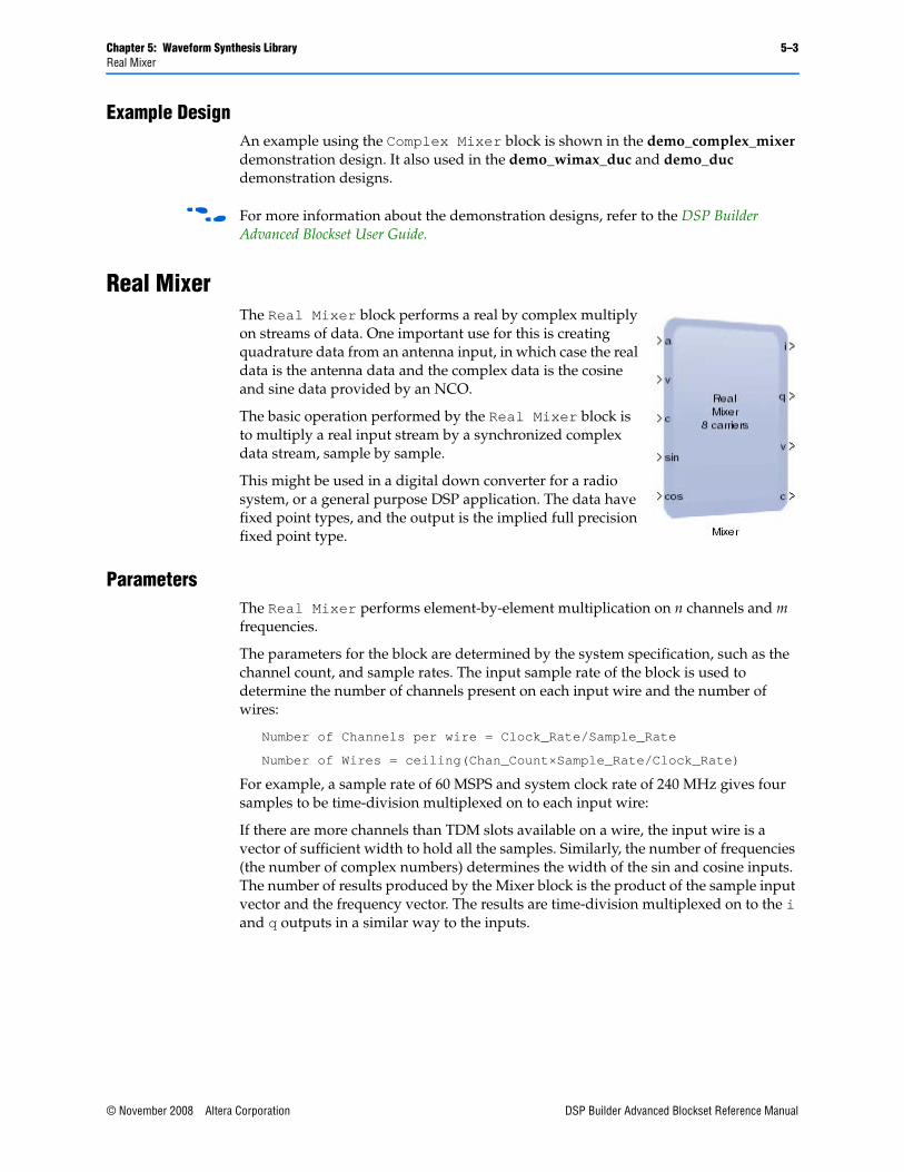
Chapter 5: Waveform Synthesis Library 5–3Real Mixer
Example DesignAn example using the Complex Mixer block is shown in the demo_complex_mixer demonstration design. It also used in the demo_wimax_duc and demo_duc demonstration designs.
f For more information about the demonstration designs, refer to the DSP Builder Advanced Blockset User Guide.
Real MixerThe Real Mixer block performs a real by complex multiply on streams of data. One important use for this is creating quadrature data from an antenna input, in which case the real data is the antenna data and the complex data is the cosine and sine data provided by an NCO.
The basic operation performed by the Real Mixer block is to multiply a real input stream by a synchronized complex data stream, sample by sample.
This might be used in a digital down converter for a radio system, or a general purpose DSP application. The data have fixed point types, and the output is the implied full precision fixed point type.
ParametersThe Real Mixer performs element-by-element multiplication on n channels and m frequencies.
The parameters for the block are determined by the system specification, such as the channel count, and sample rates. The input sample rate of the block is used to determine the number of channels present on each input wire and the number of wires:
Number of Channels per wire = Clock_Rate/Sample_Rate
Number of Wires = ceiling(Chan_Count×Sample_Rate/Clock_Rate)
For example, a sample rate of 60 MSPS and system clock rate of 240 MHz gives four samples to be time-division multiplexed on to each input wire:
If there are more channels than TDM slots available on a wire, the input wire is a vector of sufficient width to hold all the samples. Similarly, the number of frequencies (the number of complex numbers) determines the width of the sin and cosine inputs. The number of results produced by the Mixer block is the product of the sample input vector and the frequency vector. The results are time-division multiplexed on to the i and q outputs in a similar way to the inputs.
© November 2008 Altera Corporation DSP Builder Advanced Blockset Reference Manual
5–4 Chapter 5: Waveform Synthesis LibraryReal Mixer
Table 5–4 shows the parameters for the Real Mixer block.
Port InterfaceTable 5–5 shows the port interface for the Real Mixer block.
Information MessagesTable 5–6 shows typical Help messages that can be issued for the Real Mixer block.
Example DesignAn example of using the Real Mixer block is shown in the demo_mix demonstration design. It is also used in the demo_ddc demonstration design.
f For more information about the demonstration designs, refer to the DSP Builder Advanced Blockset User Guide.
Table 5–4. Parameters for the Real Mixer Block
Parameter Description
Input Rate Per Channel (MSPS) The data rate per channel measured in millions of samples per second.
Number of Channels The number of real input channels.
Number of Frequencies The number of real frequencies used in the multiplier.
Table 5–5. Port Interface for the Real Mixer Block
Signal Direction Description
a input The real data input to the block. If more channels are requested than can fit on a single bus, this signal is a vector. The bit width is inherited from the input wire.
v input Indicates validity of data input signals. If v is high the data on the a wire is valid.
c input Indicates channel of data input signals. If v is high, then c indicates the data channel.
sin input The imaginary part of the complex number. For example, the NCO's sine output for a quadrature mixer.
cos input The imaginary part of the complex number. For example, the NCO’s cosine output for a quadrature mixer.
i output The in phase (real) output of the mixer. This is (a × cos). If more channels are requested than can fit on a single bus, this signal is a vector. The bit width is wide enough for the full precision result.
q output The quadrature phase (imaginary) output of the mixer. This is (a × sin). If more channels are requested than can fit on a single bus, this signal is a vector. The bit width is wide enough for the full precision result.
v output Indicates validity of data output signals.
c output Indicates validity of data output signals.
Table 5–6. Messages for the Real Mixer Block
Message Example Description
Written on Tue Feb 19 11:25:27 2008 Date and time when this file was run.
Latency is 4 The latency introduced by this block.
Port interface table Lists the port interfaces to the Mixer block.
Resource utilization table Lists the resource utilization for the Mixer block.
DSP Builder Advanced Blockset Reference Manual © November 2008 Altera Corporation
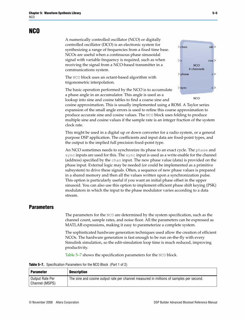
Chapter 5: Waveform Synthesis Library 5–5NCO
NCOA numerically controlled oscillator (NCO) or digitally controlled oscillator (DCO) is an electronic system for synthesizing a range of frequencies from a fixed time base. NCOs are useful when a continuous phase sinusoidal signal with variable frequency is required, such as when receiving the signal from a NCO-based transmitter in a communications system.
The NCO block uses an octant-based algorithm with trigonometric interpolation.
The basic operation performed by the NCO is to accumulate a phase angle in an accumulator. This angle is used as a lookup into sine and cosine tables to find a coarse sine and cosine approximation. This is usually implemented using a ROM. A Taylor series expansion of the small angle errors is used to refine this coarse approximation to produce accurate sine and cosine values. The NCO block uses folding to produce multiple sine and cosine values if the sample rate is an integer fraction of the system clock rate.
This might be used in a digital up or down converter for a radio system, or a general purpose DSP application. The coefficients and input data are fixed-point types, and the output is the implied full precision fixed-point type.
An NCO sometimes needs to synchronize its phase to an exact cycle. The phase and sync inputs are used for this. The sync input is used as a write enable for the channel (address) specified by the chan input. The new phase value (data) is provided on the phase input. External logic may be needed (or could be implemented as a primitive subsystem) to drive these signals. Often, a sequence of new phase values is prepared in a shared memory and then all the values written upon a synchronization pulse. This option is particularly useful if you want an initial phase offset in the upper sinusoid. You can also use this option to implement efficient phase shift keying (PSK) modulators in which the input to the phase modulator varies according to a data stream.
ParametersThe parameters for the NCO are determined by the system specification, such as the channel count, sample rates, and noise floor. All the parameters can be expressed as MATLAB expressions, making it easy to parameterize a complete system.
The sophisticated hardware generation techniques used allow the creation of efficient NCOs. The hardware generation is fast enough to be run on-the-fly with every Simulink simulation, so the edit-simulation loop time is much reduced, improving productivity.
Table 5–7 shows the specification parameters for the NCO block.
Table 5–7. Specification Parameters for the NCO Block (Part 1 of 2)
Parameter Description
Output Rate Per Channel (MSPS)
The sine and cosine output rate per channel measured in millions of samples per second.
© November 2008 Altera Corporation DSP Builder Advanced Blockset Reference Manual
5–6 Chapter 5: Waveform Synthesis LibraryNCO
The Results tab shows the implications of your parameter settings. Table 5–8 describes the parameters displayed in the Results tab.
Typical Resource UtilizationSome typical FPGA resource utilizations for a NCO using Stratix III devices are shown in Table 5–9.
Output Data Type The output width in bits of the NCO. The bit width controls the internal precision of the NCO. The spurious-free dynamic range (SFDR) of the waves produced is approximately 6.02 × bit width. The 6.02 factor comes from the definition of decibels with each added bit of precision increasing the SFDR by a factor of 20×log10(2).
Output Scaling Value This value is used to interpret the output data in the Simulink environment. The power of 2 scaling provided lets you specify the range of the output value.
Accumulator Bit Width Specifies the width of the memory mapped accumulator bit width. This governs the precision with which the NCO frequency can be controlled. The width is limited to the range 15–30 for use with a 32-bit memory map (shared by other applications such as a Nios II processor). The top two bits in the 32-bit width are reserved to control the inversion of the sine and cosine outputs. A width of 30 bits gives an accumulator precision of 0.02794 Hz. However, you can select Constant for the Read/Write Mode to allow the width to increase to 40 bits. This width results in an accumulator precision of 0.000027 MHz.
Phase Increment and Inversion
A vector that represents the step in phase to be used between each sample. This controls the frequencies that are generated during simulation. (The phase increment is a scaled and inverted version of the frequency.) The length of the vector determines how many channels of data are generated. A length four implies that four channels of data are generated. The two top bits of the phase value are used to control the inversion of the sine and cosine.
Phase Increment and Inversion Memory Map
Specifies where in the memory mapped space the NCO registers are mapped.
Read/Write Mode Specifies whether the NCO phase increment and inversion registers are mapped as Read, Write, Read/Write, or Constant.
Table 5–7. Specification Parameters for the NCO Block (Part 2 of 2)
Parameter Description
Table 5–8. Results Tab Parameters for the NCO Block
Parameter Description
Expected SFDR The SFDR in decibels relative to the carrier (dBc): (Output Data Type Width) × 20 × log10(2).
Accumulator precision Accumulator precision in Hz: 10^6 * (Output Rate) / 2^(Accumulator Bit Width+1).
Frequency Frequency in MHz: (Output Rate) * [Phase Increment And Inversion] / (2^Accumulator Bit Width).
# outputs per cycle The number of outputs per cycle is the width of the vector of output signals: Physical channels out: ceil(length[Phase Increment And Inversion]) / ((System Clock Frequency) / (Output Rate)))
log2 of look-up table The number of address bits used in the internal look-up tables.
Table 5–9. Stratix III Fitter Results for a NCO (Part 1 of 2)
Number of Frequencies
Input Rate
(MSPS)Accumulator
Width
Comb ALUTs Note 1
Logic Registers
18×18 Multipliers
Block Memory
BitsMemory ALUTs
System Frequency
(MHz)
Frequency Achieved
(MHz)
2 100 22 269 549 4 9,280 50 200 356
2 200 22 310 820 4 9,280 67 400 492
2 100 26 293 569 4 9,280 50 200 360
DSP Builder Advanced Blockset Reference Manual © November 2008 Altera Corporation

Chapter 5: Waveform Synthesis Library 5–7NCO
Port InterfaceTable 5–10 shows the port interface for the NCO block.
Information MessagesTable 5–11 shows typical Help messages that can be issued for the NCO block.
2 200 26 361 944 4 9,280 71 400 466
3 67 22 271 572 4 9,312 50 200 313
3 133 22 313 843 4 9,312 67 400 460
3 67 26 295 596 4 9,312 50 200 368
3 133 26 363 971 4 9,312 71 400 450
4 50 22 274 576 4 9,344 72 200 344
4 100 22 319 851 4 9,344 89 400 467
4 50 26 298 600 4 9,344 76 200 337
4 100 26 370 981 4 9,344 95 400 461
Notes to Table 5–9:
(1) Combinational adaptive look-up tables (ALUTs)
Table 5–9. Stratix III Fitter Results for a NCO (Part 2 of 2)
Number of Frequencies
Input Rate
(MSPS)Accumulator
Width
Comb ALUTs Note 1
Logic Registers
18×18 Multipliers
Block Memory
BitsMemory ALUTs
System Frequency
(MHz)
Frequency Achieved
(MHz)
Table 5–10. Port Interface for the NCO Block
Signal Direction Description
chan input Indicates the channel. If v is high, then chan indicates which channel the data corresponds to.
v input Indicates validity. If v is high, then new data is generated.
phase input Specifies the phase. The size of this port should match the wire count of the NCO. Note 1
sync input Specifies the phase sync. The size of this port should match the wire count of the NCO output. Note 1
sin output The sine data output from the block. If more channels are requested than can fit on a single bus, this signal is a vector. The bit width is a function of the input bit width and the parameterization.
cos output The cosine data output from the block. If more channels are requested than can fit on a single bus, this signal is vector. The bit width is a function of the input bit width and the parameterization. Note 1
v output Indicates validity of the data output signals.
c output Indicates channel of the data output signals.
Note to Table 5–10:
(1) The number of sines/cosines per cycle is currently limited to 1–16 outputs. Use multiple NCO blocks if more outputs are required.
Table 5–11. Messages for the NCO Block
Message Example Description
Written on Tue Feb 19 11:25:27 2008 Date and time when this file was run.
Latency is 16 The latency introduced by this block.
Port interface table Lists the port interfaces to the NCO block.
Resource utilization table Lists the resource utilization for the NCO block.
© November 2008 Altera Corporation DSP Builder Advanced Blockset Reference Manual

5–8 Chapter 5: Waveform Synthesis LibraryNCO
Example DesignAn example of using the NCO block is shown in the demo_nco demonstration design. It is also used in the demo_ddc, demo_duc, demo_AD9856 and demo_wimax_duc, demonstration designs.
f For more information about the demonstration designs, refer to the DSP Builder Advanced Blockset User Guide.
DSP Builder Advanced Blockset Reference Manual © November 2008 Altera Corporation
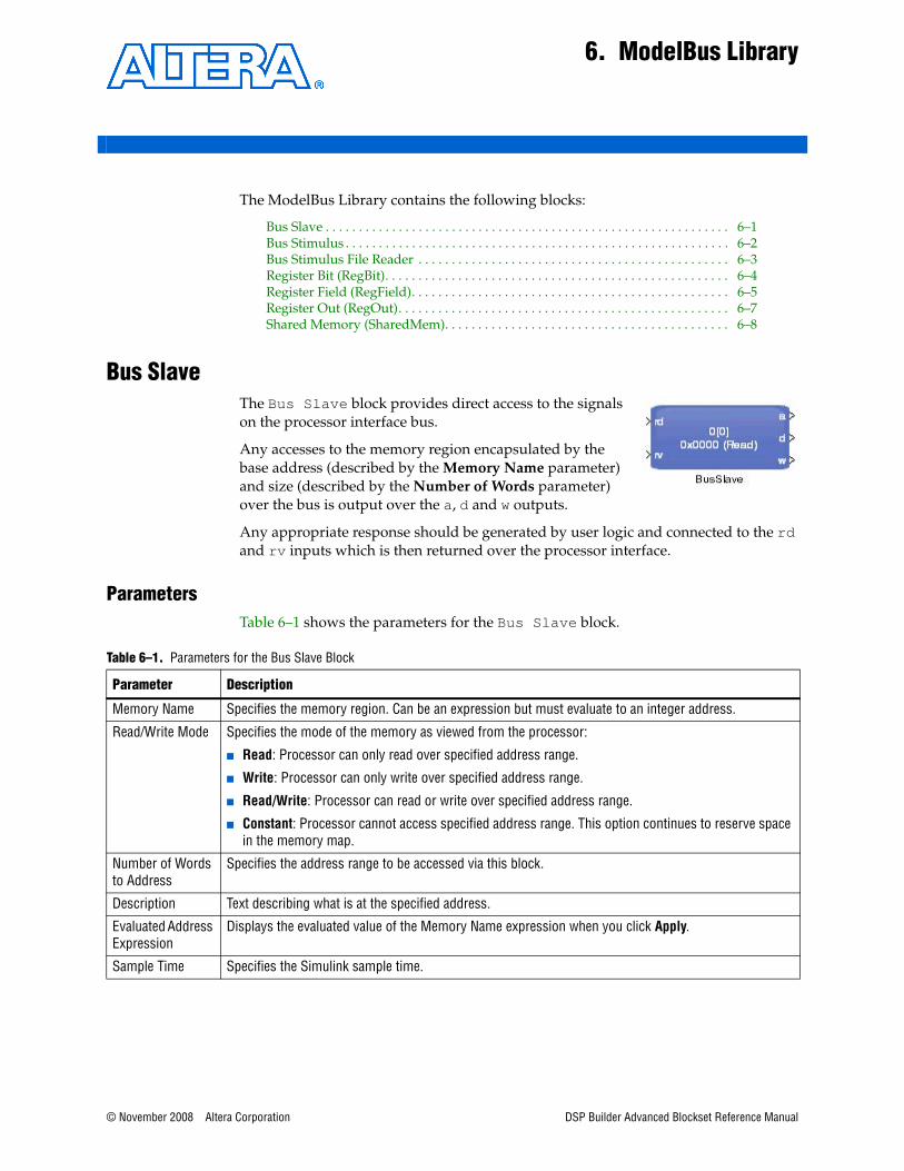
© November 2008 Altera Corporation
6. ModelBus Library
The ModelBus Library contains the following blocks:
Bus Slave . . . . . . . . . . . . . . . . . . . . . . . . . . . . . . . . . . . . . . . . . . . . . . . . . . . . . . . . . . . . . 6–1Bus Stimulus . . . . . . . . . . . . . . . . . . . . . . . . . . . . . . . . . . . . . . . . . . . . . . . . . . . . . . . . . . 6–2Bus Stimulus File Reader . . . . . . . . . . . . . . . . . . . . . . . . . . . . . . . . . . . . . . . . . . . . . . . 6–3Register Bit (RegBit). . . . . . . . . . . . . . . . . . . . . . . . . . . . . . . . . . . . . . . . . . . . . . . . . . . . 6–4Register Field (RegField). . . . . . . . . . . . . . . . . . . . . . . . . . . . . . . . . . . . . . . . . . . . . . . . 6–5Register Out (RegOut). . . . . . . . . . . . . . . . . . . . . . . . . . . . . . . . . . . . . . . . . . . . . . . . . . 6–7Shared Memory (SharedMem). . . . . . . . . . . . . . . . . . . . . . . . . . . . . . . . . . . . . . . . . . . 6–8
Bus SlaveThe Bus Slave block provides direct access to the signals on the processor interface bus.
Any accesses to the memory region encapsulated by the base address (described by the Memory Name parameter) and size (described by the Number of Words parameter) over the bus is output over the a, d and w outputs.
Any appropriate response should be generated by user logic and connected to the rd and rv inputs which is then returned over the processor interface.
ParametersTable 6–1 shows the parameters for the Bus Slave block.
Table 6–1. Parameters for the Bus Slave Block
Parameter Description
Memory Name Specifies the memory region. Can be an expression but must evaluate to an integer address.
Read/Write Mode Specifies the mode of the memory as viewed from the processor:
■ Read: Processor can only read over specified address range.
■ Write: Processor can only write over specified address range.
■ Read/Write: Processor can read or write over specified address range.
■ Constant: Processor cannot access specified address range. This option continues to reserve space in the memory map.
Number of Words to Address
Specifies the address range to be accessed via this block.
Description Text describing what is at the specified address.
Evaluated Address Expression
Displays the evaluated value of the Memory Name expression when you click Apply.
Sample Time Specifies the Simulink sample time.
DSP Builder Advanced Blockset Reference Manual
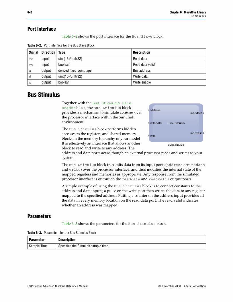
6–2 Chapter 6: ModelBus LibraryBus Stimulus
Port InterfaceTable 6–2 shows the port interface for the Bus Slave block.
Bus StimulusTogether with the Bus Stimulus File Reader block, the Bus Stimulus block provides a mechanism to simulate accesses over the processor interface within the Simulink environment.
The Bus Stimulus block performs hidden accesses to the registers and shared memory blocks in the memory hierarchy of your model It is effectively an interface that allows another block to read and write to any address. The address and data ports act as though an external processor reads and writes to your system.
The Bus Stimulus block transmits data from its input ports (address, writedata and write) over the processor interface, and thus modifies the internal state of the mapped registers and memories as appropriate. Any response from the simulated processor interface is output on the readdata and readvalid output ports.
A simple example of using the Bus Stimulus block is to connect constants to the address and data inputs; a pulse on the write port then writes the data to any register mapped to the specified address. Putting a counter on the address input provides all the data in every memory location on the read data port. The read valid indicates whether an address was mapped.
ParametersTable 6–3 shows the parameters for the Bus Stimulus block.
Table 6–2. Port Interface for the Bus Slave Block
Signal Direction Type Description
rd input uint(16)/uint(32) Read data
rv input boolean Read data valid
a output derived fixed point type Bus address
d output uint(16)/uint(32) Write data
w output boolean Write enable
Table 6–3. Parameters for the Bus Stimulus Block
Parameter Description
Sample Time Specifies the Simulink sample time.
DSP Builder Advanced Blockset Reference Manual © November 2008 Altera Corporation
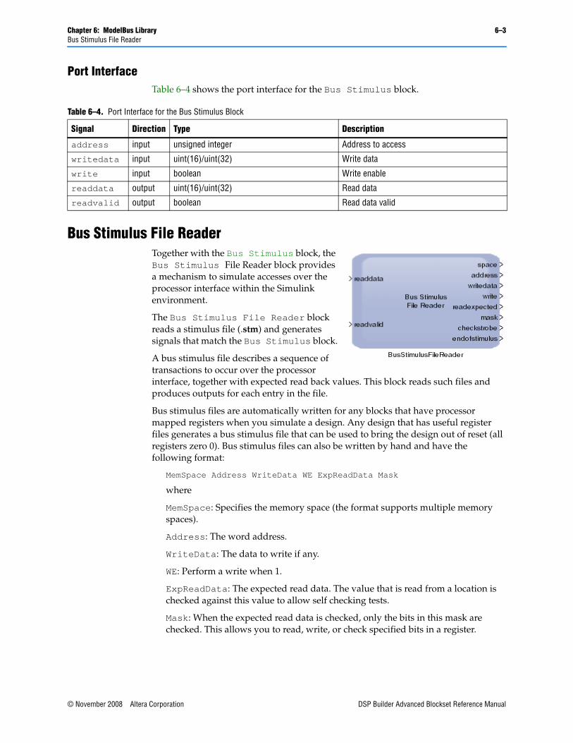
Chapter 6: ModelBus Library 6–3Bus Stimulus File Reader
Port InterfaceTable 6–4 shows the port interface for the Bus Stimulus block.
Bus Stimulus File ReaderTogether with the Bus Stimulus block, the Bus Stimulus File Reader block provides a mechanism to simulate accesses over the processor interface within the Simulink environment.
The Bus Stimulus File Reader block reads a stimulus file (.stm) and generates signals that match the Bus Stimulus block.
A bus stimulus file describes a sequence of transactions to occur over the processor interface, together with expected read back values. This block reads such files and produces outputs for each entry in the file.
Bus stimulus files are automatically written for any blocks that have processor mapped registers when you simulate a design. Any design that has useful register files generates a bus stimulus file that can be used to bring the design out of reset (all registers zero 0). Bus stimulus files can also be written by hand and have the following format:
MemSpace Address WriteData WE ExpReadData Mask
where
MemSpace: Specifies the memory space (the format supports multiple memory spaces).
Address: The word address.
WriteData: The data to write if any.
WE: Perform a write when 1.
ExpReadData: The expected read data. The value that is read from a location is checked against this value to allow self checking tests.
Mask: When the expected read data is checked, only the bits in this mask are checked. This allows you to read, write, or check specified bits in a register.
Table 6–4. Port Interface for the Bus Stimulus Block
Signal Direction Type Description
address input unsigned integer Address to access
writedata input uint(16)/uint(32) Write data
write input boolean Write enable
readdata output uint(16)/uint(32) Read data
readvalid output boolean Read data valid
© November 2008 Altera Corporation DSP Builder Advanced Blockset Reference Manual

6–4 Chapter 6: ModelBus LibraryRegister Bit (RegBit)
During simulation, any mismatch between the expected read data (as described in the bus stimulus file) and the incoming read data (provided by the BusStimulus block) is highlighted and a warning is issued.
ParametersTable 6–5 shows the parameters for the Bus Stimulus File Reader block.
Port InterfaceTable 6–6 shows the port interface for the Bus Stimulus File Reader block.
Register Bit (RegBit)The Register Bit block provides a register bit accessible in the model and via the processor interface.
Table 6–5. Parameters for the Bus Stimulus File Reader Block
Parameter Description
Enabled Turn on to enable reading of the bus stimulus file data.
Stimulus File Name Specifies the file from which to read bus stimulus data.
Log File Name Specifies the file to store a log of all attempted bus stimulus accesses.
Space Width Specifies the width of the memory space as described in the bus stimulus file. (This must be same as the width specified in the Control block.)
Addr Width Specifies the width of the address space as described in the bus stimulus file. (This must be the same as the width specified in the Control block.)
Data Width Specifies the width of the data width as described in the bus stimulus file (must be same as Control).
Sample Time Specifies the Simulink sample time.
Table 6–6. Port Interface for the Bus Stimulus File Reader Block
Signal Direction Type Description
readdata input uint(16)/uint(32) Read data.
readvalid input boolean Read data valid.
space output unsigned integer Memory space from file.
address output unsigned integer Address from file.
writedata output uint(16)/uint(32) Data from file.
write output boolean Write signal from file.
readexpected output uint(16)/uint(32) Expected read data from file.
mask output uint(16)/uint(32) Mask value from file.
checkstrobe output boolean Generated signal which indicates when the readexpected and mask signals should be checked against readdata.
endofstimulus output boolean Generated signal to indicate when the end of the bus stimulus file is reached.
DSP Builder Advanced Blockset Reference Manual © November 2008 Altera Corporation
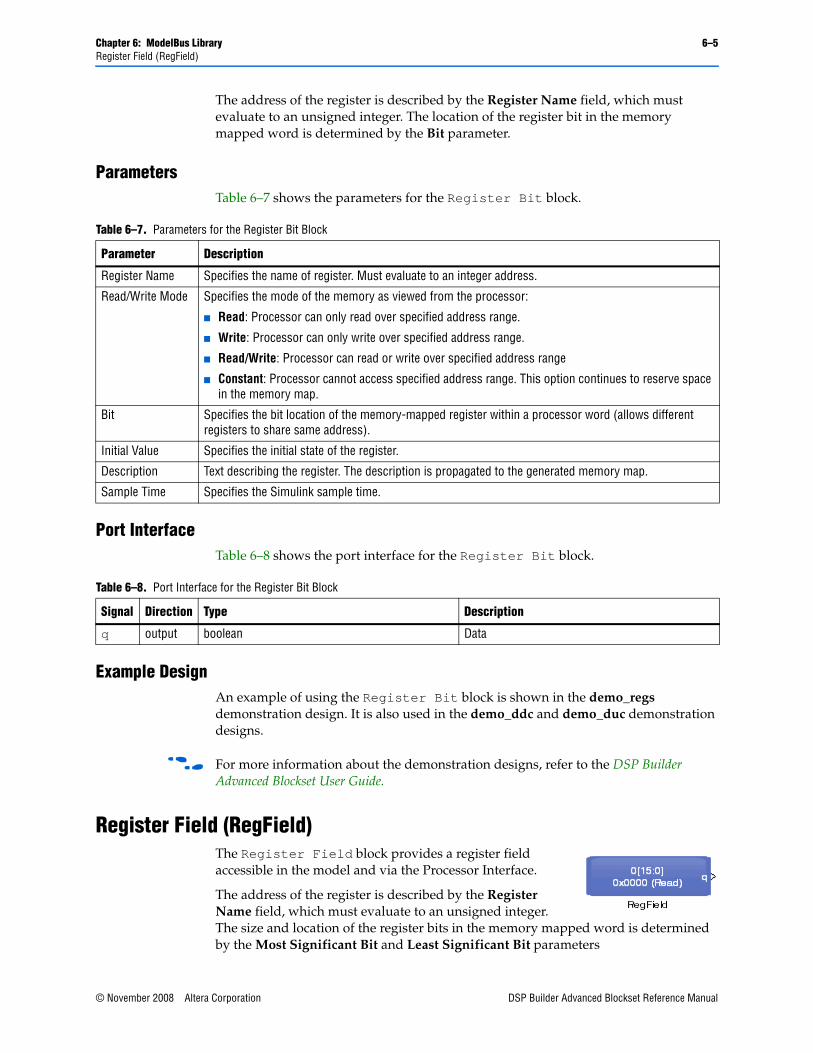
Chapter 6: ModelBus Library 6–5Register Field (RegField)
The address of the register is described by the Register Name field, which must evaluate to an unsigned integer. The location of the register bit in the memory mapped word is determined by the Bit parameter.
ParametersTable 6–7 shows the parameters for the Register Bit block.
Port InterfaceTable 6–8 shows the port interface for the Register Bit block.
Example DesignAn example of using the Register Bit block is shown in the demo_regs demonstration design. It is also used in the demo_ddc and demo_duc demonstration designs.
f For more information about the demonstration designs, refer to the DSP Builder Advanced Blockset User Guide.
Register Field (RegField)The Register Field block provides a register field accessible in the model and via the Processor Interface.
The address of the register is described by the Register Name field, which must evaluate to an unsigned integer. The size and location of the register bits in the memory mapped word is determined by the Most Significant Bit and Least Significant Bit parameters
Table 6–7. Parameters for the Register Bit Block
Parameter Description
Register Name Specifies the name of register. Must evaluate to an integer address.
Read/Write Mode Specifies the mode of the memory as viewed from the processor:
■ Read: Processor can only read over specified address range.
■ Write: Processor can only write over specified address range.
■ Read/Write: Processor can read or write over specified address range
■ Constant: Processor cannot access specified address range. This option continues to reserve space in the memory map.
Bit Specifies the bit location of the memory-mapped register within a processor word (allows different registers to share same address).
Initial Value Specifies the initial state of the register.
Description Text describing the register. The description is propagated to the generated memory map.
Sample Time Specifies the Simulink sample time.
Table 6–8. Port Interface for the Register Bit Block
Signal Direction Type Description
q output boolean Data
© November 2008 Altera Corporation DSP Builder Advanced Blockset Reference Manual

6–6 Chapter 6: ModelBus LibraryRegister Field (RegField)
ParametersTable 6–9 shows the parameters for the Register Field block.
Port InterfaceTable 6–10 shows the port interface for the Register Field block.
Example DesignAn example of using the Register Field block is shown in the demo_regs demonstration design. It is also used in the demo_agc, demo_ddc and demo_duc demonstration designs.
f For more information about the demonstration designs, refer to the DSP Builder Advanced Blockset User Guide.
Table 6–9. Parameters for the Register Field Block
Parameter Description
Register Name Specifies the name of register. Must evaluate to an integer address.
Read/Write Mode Specifies the mode of the memory as viewed from the processor:
■ Read: Processor can only read over specified address range.
■ Write: Processor can only write over specified address range.
■ Read/Write: Processor can read or write over specified address range
■ Constant: Processor cannot access specified address range. This option continues to reserve space in the memory map.
Most Significant Bit
Specifies the MSB of the memory-mapped register within a processor word (allows different registers to share same address).
Least Significant Bit
Specifies the LSB of the memory-mapped register within a processor word (allows different registers to share same address).
Register Output Type
Specifies the data type that is being stored in the register. The size should equal (MSB–LSB+1).
Register Output Scale
Specifies the data type that is being stored in the register.
Initial Value Specifies the initial state of the register.
Description Text describing the register. The description is propagated to the generated memory map.
Modal Behavior Turn on if you want to enable modal behavior.
Sample Time Specifies the Simulink sample time.
Table 6–10. Port Interface for the Register Field Block
Signal Direction Type Description
q output Any fixed point type. Data
DSP Builder Advanced Blockset Reference Manual © November 2008 Altera Corporation

Chapter 6: ModelBus Library 6–7Register Out (RegOut)
Register Out (RegOut)The Register Out block provides a register field accessible in the model and via the Processor Interface.
The address of the register is described by the Register Name field, which must evaluate to an unsigned integer. The size and location of the register bits in the memory mapped word is determined by the Most Significant Bit and Least Significant Bit parameters
ParametersTable 6–11 shows the parameters for the Register Out block.
Port InterfaceTable 6–12 shows the port interface for the Register Out block.
Example DesignAn example of using the Register Out block is shown in the demo_regs demonstration design.
f For more information about the demonstration designs, refer to the DSP Builder Advanced Blockset User Guide.
Table 6–11. Parameters for the Register Out Block
Parameter Description
Register Name Specifies the name of register. Must evaluate to an integer address.
Read/Write Mode Specifies the mode of the memory as viewed from the processor:
■ Read: Processor can only read over specified address range.
■ Write: Processor can only write over specified address range.
■ Read/Write: Processor can read or write over specified address range
■ Constant: Processor cannot access specified address range. This option continues to reserve space in the memory map.
Most Significant Bit
Specifies the MSB of the memory-mapped register within a processor word (allows different registers to share same address).
Least Significant Bit
Specifies the LSB of the memory-mapped register within a processor word (allows different registers to share same address).
Description Text describing the register. The description is propagated to the generated memory map.
Modal Behavior Turn on if you want to enable modal behavior.
Sample Time Specifies the Simulink sample time.
Table 6–12. Port Interface for the Register Out Block
Signal Direction Type Description
d input Any fixed point type Data.
w input boolean Write data.
© November 2008 Altera Corporation DSP Builder Advanced Blockset Reference Manual
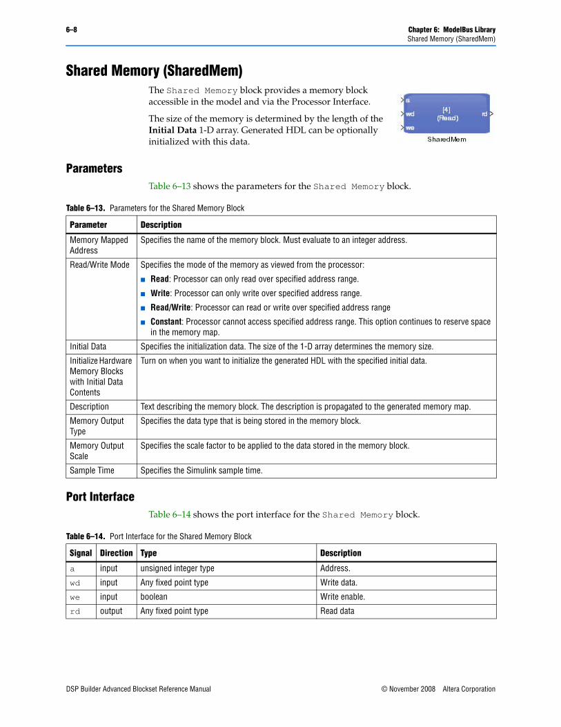
6–8 Chapter 6: ModelBus LibraryShared Memory (SharedMem)
Shared Memory (SharedMem)The Shared Memory block provides a memory block accessible in the model and via the Processor Interface.
The size of the memory is determined by the length of the Initial Data 1-D array. Generated HDL can be optionally initialized with this data.
ParametersTable 6–13 shows the parameters for the Shared Memory block.
Port InterfaceTable 6–14 shows the port interface for the Shared Memory block.
Table 6–13. Parameters for the Shared Memory Block
Parameter Description
Memory Mapped Address
Specifies the name of the memory block. Must evaluate to an integer address.
Read/Write Mode Specifies the mode of the memory as viewed from the processor:
■ Read: Processor can only read over specified address range.
■ Write: Processor can only write over specified address range.
■ Read/Write: Processor can read or write over specified address range
■ Constant: Processor cannot access specified address range. This option continues to reserve space in the memory map.
Initial Data Specifies the initialization data. The size of the 1-D array determines the memory size.
Initialize Hardware Memory Blocks with Initial Data Contents
Turn on when you want to initialize the generated HDL with the specified initial data.
Description Text describing the memory block. The description is propagated to the generated memory map.
Memory Output Type
Specifies the data type that is being stored in the memory block.
Memory Output Scale
Specifies the scale factor to be applied to the data stored in the memory block.
Sample Time Specifies the Simulink sample time.
Table 6–14. Port Interface for the Shared Memory Block
Signal Direction Type Description
a input unsigned integer type Address.
wd input Any fixed point type Write data.
we input boolean Write enable.
rd output Any fixed point type Read data
DSP Builder Advanced Blockset Reference Manual © November 2008 Altera Corporation

Chapter 6: ModelBus Library 6–9Shared Memory (SharedMem)
Example DesignAn example of using the Shared Memory block is shown in the demo_regs demonstration design. It is also used in the demo_agc demonstration design.
f For more information about the demonstration designs, refer to the DSP Builder Advanced Blockset User Guide.
© November 2008 Altera Corporation DSP Builder Advanced Blockset Reference Manual

6–10 Chapter 6: ModelBus LibraryShared Memory (SharedMem)
DSP Builder Advanced Blockset Reference Manual © November 2008 Altera Corporation
© November 2008 Altera Corporation
7. ModelPrim Library
The ModelPrim Library contains the following primitive blocks:
Absolute Value (Abs) . . . . . . . . . . . . . . . . . . . . . . . . . . . . . . . . . . . . . . . . . . . . . . . . . . 7–2Add . . . . . . . . . . . . . . . . . . . . . . . . . . . . . . . . . . . . . . . . . . . . . . . . . . . . . . . . . . . . . . . . . 7–3Add SLoad . . . . . . . . . . . . . . . . . . . . . . . . . . . . . . . . . . . . . . . . . . . . . . . . . . . . . . . . . . . 7–4AND Gate (And) . . . . . . . . . . . . . . . . . . . . . . . . . . . . . . . . . . . . . . . . . . . . . . . . . . . . . . 7–5Bit Combine . . . . . . . . . . . . . . . . . . . . . . . . . . . . . . . . . . . . . . . . . . . . . . . . . . . . . . . . . . 7–6Bit Extract . . . . . . . . . . . . . . . . . . . . . . . . . . . . . . . . . . . . . . . . . . . . . . . . . . . . . . . . . . . . 7–7Bit Reverse. . . . . . . . . . . . . . . . . . . . . . . . . . . . . . . . . . . . . . . . . . . . . . . . . . . . . . . . . . . . 7–8Channel In. . . . . . . . . . . . . . . . . . . . . . . . . . . . . . . . . . . . . . . . . . . . . . . . . . . . . . . . . . . . 7–9Channel Out . . . . . . . . . . . . . . . . . . . . . . . . . . . . . . . . . . . . . . . . . . . . . . . . . . . . . . . . . 7–10Count Leading Zeros (CLZ) . . . . . . . . . . . . . . . . . . . . . . . . . . . . . . . . . . . . . . . . . . . . 7–11Compare Equality (CmpEQ) . . . . . . . . . . . . . . . . . . . . . . . . . . . . . . . . . . . . . . . . . . . 7–12Compare Greater Than (CmpGE) . . . . . . . . . . . . . . . . . . . . . . . . . . . . . . . . . . . . . . . 7–13Compare Less Than (CmpLT) . . . . . . . . . . . . . . . . . . . . . . . . . . . . . . . . . . . . . . . . . . 7–14Compare Not Equal (CmpNE). . . . . . . . . . . . . . . . . . . . . . . . . . . . . . . . . . . . . . . . . . 7–14Constant (Const) . . . . . . . . . . . . . . . . . . . . . . . . . . . . . . . . . . . . . . . . . . . . . . . . . . . . . 7–15Convert . . . . . . . . . . . . . . . . . . . . . . . . . . . . . . . . . . . . . . . . . . . . . . . . . . . . . . . . . . . . . 7–16CORDIC . . . . . . . . . . . . . . . . . . . . . . . . . . . . . . . . . . . . . . . . . . . . . . . . . . . . . . . . . . . . 7–17Counter . . . . . . . . . . . . . . . . . . . . . . . . . . . . . . . . . . . . . . . . . . . . . . . . . . . . . . . . . . . . . 7–19Delay . . . . . . . . . . . . . . . . . . . . . . . . . . . . . . . . . . . . . . . . . . . . . . . . . . . . . . . . . . . . . . . 7–20Dual Memory (DualMem) . . . . . . . . . . . . . . . . . . . . . . . . . . . . . . . . . . . . . . . . . . . . . 7–21General Purpose Input (GPIn) . . . . . . . . . . . . . . . . . . . . . . . . . . . . . . . . . . . . . . . . . . 7–22General Purpose Output (GPOut). . . . . . . . . . . . . . . . . . . . . . . . . . . . . . . . . . . . . . . 7–23Left Shift (LShift) . . . . . . . . . . . . . . . . . . . . . . . . . . . . . . . . . . . . . . . . . . . . . . . . . . . . . 7–24Look-Up Table (Lut) . . . . . . . . . . . . . . . . . . . . . . . . . . . . . . . . . . . . . . . . . . . . . . . . . . 7–25Maximum Value (Max) . . . . . . . . . . . . . . . . . . . . . . . . . . . . . . . . . . . . . . . . . . . . . . . . 7–26Minimum Value (Min) . . . . . . . . . . . . . . . . . . . . . . . . . . . . . . . . . . . . . . . . . . . . . . . . 7–27Multiply (Mult) . . . . . . . . . . . . . . . . . . . . . . . . . . . . . . . . . . . . . . . . . . . . . . . . . . . . . . 7–28Multiplexer (Mux2) . . . . . . . . . . . . . . . . . . . . . . . . . . . . . . . . . . . . . . . . . . . . . . . . . . . 7–29NAND Gate (Nand). . . . . . . . . . . . . . . . . . . . . . . . . . . . . . . . . . . . . . . . . . . . . . . . . . . 7–30NOR Gate (Nor) . . . . . . . . . . . . . . . . . . . . . . . . . . . . . . . . . . . . . . . . . . . . . . . . . . . . . . 7–31NOT Gate (Not) . . . . . . . . . . . . . . . . . . . . . . . . . . . . . . . . . . . . . . . . . . . . . . . . . . . . . . 7–32OR Gate (Or) . . . . . . . . . . . . . . . . . . . . . . . . . . . . . . . . . . . . . . . . . . . . . . . . . . . . . . . . . 7–33Sample Delay . . . . . . . . . . . . . . . . . . . . . . . . . . . . . . . . . . . . . . . . . . . . . . . . . . . . . . . . 7–34Select . . . . . . . . . . . . . . . . . . . . . . . . . . . . . . . . . . . . . . . . . . . . . . . . . . . . . . . . . . . . . . . 7–35Sequence . . . . . . . . . . . . . . . . . . . . . . . . . . . . . . . . . . . . . . . . . . . . . . . . . . . . . . . . . . . . 7–36Shift . . . . . . . . . . . . . . . . . . . . . . . . . . . . . . . . . . . . . . . . . . . . . . . . . . . . . . . . . . . . . . . . 7–37Subtract (Sub) . . . . . . . . . . . . . . . . . . . . . . . . . . . . . . . . . . . . . . . . . . . . . . . . . . . . . . . . 7–38Synthesis Information (SynthesisInfo) . . . . . . . . . . . . . . . . . . . . . . . . . . . . . . . . . . . 7–39XNOR Gate (Xnor). . . . . . . . . . . . . . . . . . . . . . . . . . . . . . . . . . . . . . . . . . . . . . . . . . . . 7–40XOR Gate (Xor). . . . . . . . . . . . . . . . . . . . . . . . . . . . . . . . . . . . . . . . . . . . . . . . . . . . . . . 7–41
DSP Builder Advanced Blockset Reference Manual
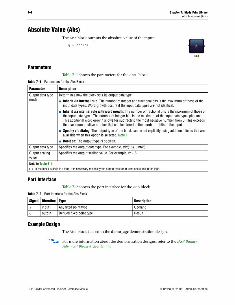
7–2 Chapter 7: ModelPrim LibraryAbsolute Value (Abs)
Absolute Value (Abs)The Abs block outputs the absolute value of the input:
q = abs(a)
ParametersTable 7–1 shows the parameters for the Abs block.
Port InterfaceTable 7–2 shows the port interface for the Abs block.
Example DesignThe Abs block is used in the demo_agc demonstration design.
f For more information about the demonstration designs, refer to the DSP Builder Advanced Blockset User Guide.
Table 7–1. Parameters for the Abs Block
Parameter Description
Output data type mode
Determines how the block sets its output data type:
■ Inherit via internal rule: The number of integer and fractional bits is the maximum of those of the input data types. Word growth occurs if the input data types are not identical.
■ Inherit via internal rule with word growth: The number of fractional bits is the maximum of those of the input data types. The number of integer bits is the maximum of the input data types plus one. This additional word growth allows for subtracting the most negative number from 0. This exceeds the maximum positive number that can be stored in the number of bits of the input.
■ Specify via dialog: The output type of the block can be set explicitly using additional fields that are available when this option is selected. Note 1
■ Boolean: The output type is boolean.
Output data type Specifies the output data type. For example, sfix(16), uint(8).
Output scaling value
Specifies the output scaling value. For example, 2^-15.
Note to Table 7–1:
(1) If the block is used in a loop, it is necessary to specify the output type for at least one block in the loop.
Table 7–2. Port Interface for the Abs Block
Signal Direction Type Description
a input Any fixed point type Operand
q output Derived fixed point type Result
DSP Builder Advanced Blockset Reference Manual © November 2008 Altera Corporation
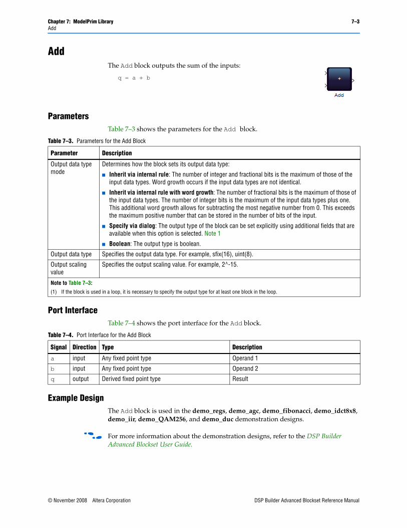
Chapter 7: ModelPrim Library 7–3Add
AddThe Add block outputs the sum of the inputs:
q = a + b
ParametersTable 7–3 shows the parameters for the Add block.
Port InterfaceTable 7–4 shows the port interface for the Add block.
Example DesignThe Add block is used in the demo_regs, demo_agc, demo_fibonacci, demo_idct8x8, demo_iir, demo_QAM256, and demo_duc demonstration designs.
f For more information about the demonstration designs, refer to the DSP Builder Advanced Blockset User Guide.
Table 7–3. Parameters for the Add Block
Parameter Description
Output data type mode
Determines how the block sets its output data type:
■ Inherit via internal rule: The number of integer and fractional bits is the maximum of those of the input data types. Word growth occurs if the input data types are not identical.
■ Inherit via internal rule with word growth: The number of fractional bits is the maximum of those of the input data types. The number of integer bits is the maximum of the input data types plus one. This additional word growth allows for subtracting the most negative number from 0. This exceeds the maximum positive number that can be stored in the number of bits of the input.
■ Specify via dialog: The output type of the block can be set explicitly using additional fields that are available when this option is selected. Note 1
■ Boolean: The output type is boolean.
Output data type Specifies the output data type. For example, sfix(16), uint(8).
Output scaling value
Specifies the output scaling value. For example, 2^-15.
Note to Table 7–3:
(1) If the block is used in a loop, it is necessary to specify the output type for at least one block in the loop.
Table 7–4. Port Interface for the Add Block
Signal Direction Type Description
a input Any fixed point type Operand 1
b input Any fixed point type Operand 2
q output Derived fixed point type Result
© November 2008 Altera Corporation DSP Builder Advanced Blockset Reference Manual
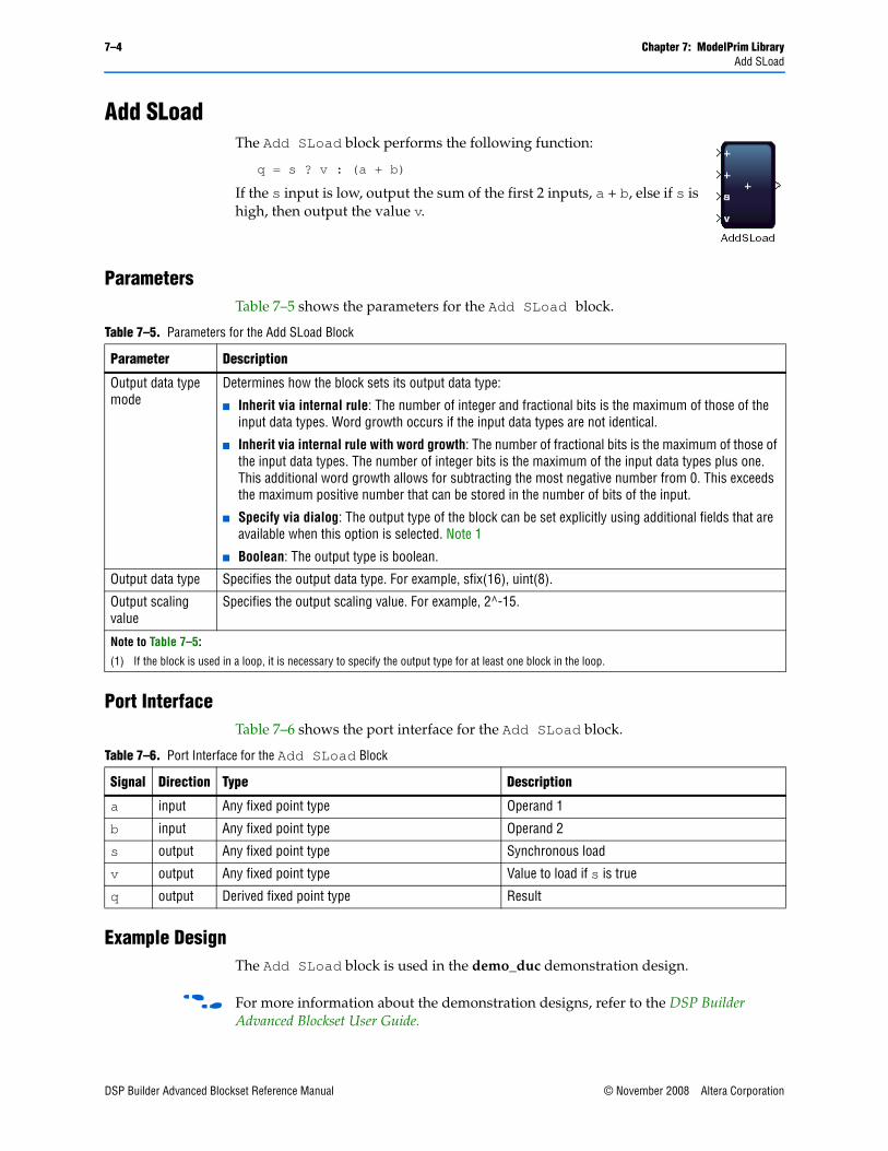
7–4 Chapter 7: ModelPrim LibraryAdd SLoad
Add SLoadThe Add SLoad block performs the following function:
q = s ? v : (a + b)
If the s input is low, output the sum of the first 2 inputs, a + b, else if s is high, then output the value v.
ParametersTable 7–5 shows the parameters for the Add SLoad block.
Port InterfaceTable 7–6 shows the port interface for the Add SLoad block.
Example DesignThe Add SLoad block is used in the demo_duc demonstration design.
f For more information about the demonstration designs, refer to the DSP Builder Advanced Blockset User Guide.
Table 7–5. Parameters for the Add SLoad Block
Parameter Description
Output data type mode
Determines how the block sets its output data type:
■ Inherit via internal rule: The number of integer and fractional bits is the maximum of those of the input data types. Word growth occurs if the input data types are not identical.
■ Inherit via internal rule with word growth: The number of fractional bits is the maximum of those of the input data types. The number of integer bits is the maximum of the input data types plus one. This additional word growth allows for subtracting the most negative number from 0. This exceeds the maximum positive number that can be stored in the number of bits of the input.
■ Specify via dialog: The output type of the block can be set explicitly using additional fields that are available when this option is selected. Note 1
■ Boolean: The output type is boolean.
Output data type Specifies the output data type. For example, sfix(16), uint(8).
Output scaling value
Specifies the output scaling value. For example, 2^-15.
Note to Table 7–5:
(1) If the block is used in a loop, it is necessary to specify the output type for at least one block in the loop.
Table 7–6. Port Interface for the Add SLoad Block
Signal Direction Type Description
a input Any fixed point type Operand 1
b input Any fixed point type Operand 2
s output Any fixed point type Synchronous load
v output Any fixed point type Value to load if s is true
q output Derived fixed point type Result
DSP Builder Advanced Blockset Reference Manual © November 2008 Altera Corporation
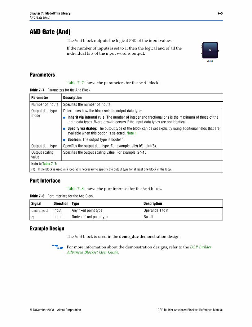
Chapter 7: ModelPrim Library 7–5AND Gate (And)
AND Gate (And)The And block outputs the logical AND of the input values.
If the number of inputs is set to 1, then the logical and of all the individual bits of the input word is output.
ParametersTable 7–7 shows the parameters for the And block.
Port InterfaceTable 7–8 shows the port interface for the And block.
Example DesignThe And block is used in the demo_duc demonstration design.
f For more information about the demonstration designs, refer to the DSP Builder Advanced Blockset User Guide.
Table 7–7. Parameters for the And Block
Parameter Description
Number of inputs Specifies the number of inputs.
Output data type mode
Determines how the block sets its output data type:
■ Inherit via internal rule: The number of integer and fractional bits is the maximum of those of the input data types. Word growth occurs if the input data types are not identical.
■ Specify via dialog: The output type of the block can be set explicitly using additional fields that are available when this option is selected. Note 1
■ Boolean: The output type is boolean.
Output data type Specifies the output data type. For example, sfix(16), uint(8).
Output scaling value
Specifies the output scaling value. For example, 2^-15.
Note to Table 7–7:
(1) If the block is used in a loop, it is necessary to specify the output type for at least one block in the loop.
Table 7–8. Port Interface for the And Block
Signal Direction Type Description
unnamed input Any fixed point type Operands 1 to n
q output Derived fixed point type Result
© November 2008 Altera Corporation DSP Builder Advanced Blockset Reference Manual
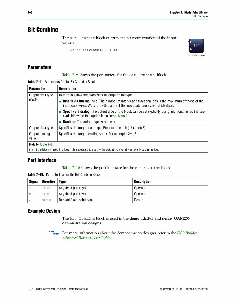
7–6 Chapter 7: ModelPrim LibraryBit Combine
Bit CombineThe Bit Combine block outputs the bit concatenation of the input values:
((h << bitwidth(i)) | i)
ParametersTable 7–9 shows the parameters for the Bit Combine block.
Port InterfaceTable 7–10 shows the port interface for the Bit Combine block.
Example DesignThe Bit Combine block is used in the demo_idct8x8 and demo_QAM256 demonstration designs.
f For more information about the demonstration designs, refer to the DSP Builder Advanced Blockset User Guide.
Table 7–9. Parameters for the Bit Combine Block
Parameter Description
Output data type mode
Determines how the block sets its output data type:
■ Inherit via internal rule: The number of integer and fractional bits is the maximum of those of the input data types. Word growth occurs if the input data types are not identical.
■ Specify via dialog: The output type of the block can be set explicitly using additional fields that are available when this option is selected. Note 1
■ Boolean: The output type is boolean.
Output data type Specifies the output data type. For example, sfix(16), uint(8).
Output scaling value
Specifies the output scaling value. For example, 2^-15.
Note to Table 7–9:
(1) If the block is used in a loop, it is necessary to specify the output type for at least one block in the loop.
Table 7–10. Port Interface for the Bit Combine Block
Signal Direction Type Description
i input Any fixed point type Operand
h input Any fixed point type Operand
q output Derived fixed point type Result
DSP Builder Advanced Blockset Reference Manual © November 2008 Altera Corporation
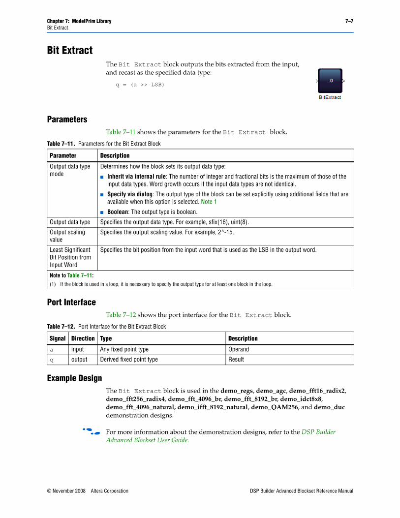
Chapter 7: ModelPrim Library 7–7Bit Extract
Bit ExtractThe Bit Extract block outputs the bits extracted from the input, and recast as the specified data type:
q = (a >> LSB)
ParametersTable 7–11 shows the parameters for the Bit Extract block.
Port InterfaceTable 7–12 shows the port interface for the Bit Extract block.
Example DesignThe Bit Extract block is used in the demo_regs, demo_agc, demo_fft16_radix2, demo_fft256_radix4, demo_fft_4096_br, demo_fft_8192_br, demo_idct8x8, demo_fft_4096_natural, demo_ifft_8192_natural, demo_QAM256, and demo_duc demonstration designs.
f For more information about the demonstration designs, refer to the DSP Builder Advanced Blockset User Guide.
Table 7–11. Parameters for the Bit Extract Block
Parameter Description
Output data type mode
Determines how the block sets its output data type:
■ Inherit via internal rule: The number of integer and fractional bits is the maximum of those of the input data types. Word growth occurs if the input data types are not identical.
■ Specify via dialog: The output type of the block can be set explicitly using additional fields that are available when this option is selected. Note 1
■ Boolean: The output type is boolean.
Output data type Specifies the output data type. For example, sfix(16), uint(8).
Output scaling value
Specifies the output scaling value. For example, 2^-15.
Least Significant Bit Position from Input Word
Specifies the bit position from the input word that is used as the LSB in the output word.
Note to Table 7–11:
(1) If the block is used in a loop, it is necessary to specify the output type for at least one block in the loop.
Table 7–12. Port Interface for the Bit Extract Block
Signal Direction Type Description
a input Any fixed point type Operand
q output Derived fixed point type Result
© November 2008 Altera Corporation DSP Builder Advanced Blockset Reference Manual
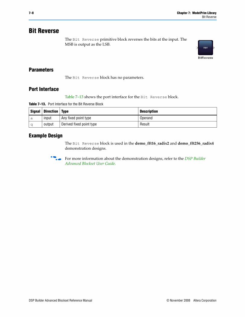
7–8 Chapter 7: ModelPrim LibraryBit Reverse
Bit ReverseThe Bit Reverse primitive block reverses the bits at the input. The MSB is output as the LSB.
ParametersThe Bit Reverse block has no parameters.
Port InterfaceTable 7–13 shows the port interface for the Bit Reverse block.
Example DesignThe Bit Reverse block is used in the demo_fft16_radix2 and demo_fft256_radix4 demonstration designs.
f For more information about the demonstration designs, refer to the DSP Builder Advanced Blockset User Guide.
Table 7–13. Port Interface for the Bit Reverse Block
Signal Direction Type Description
a input Any fixed point type Operand
q output Derived fixed point type Result
DSP Builder Advanced Blockset Reference Manual © November 2008 Altera Corporation
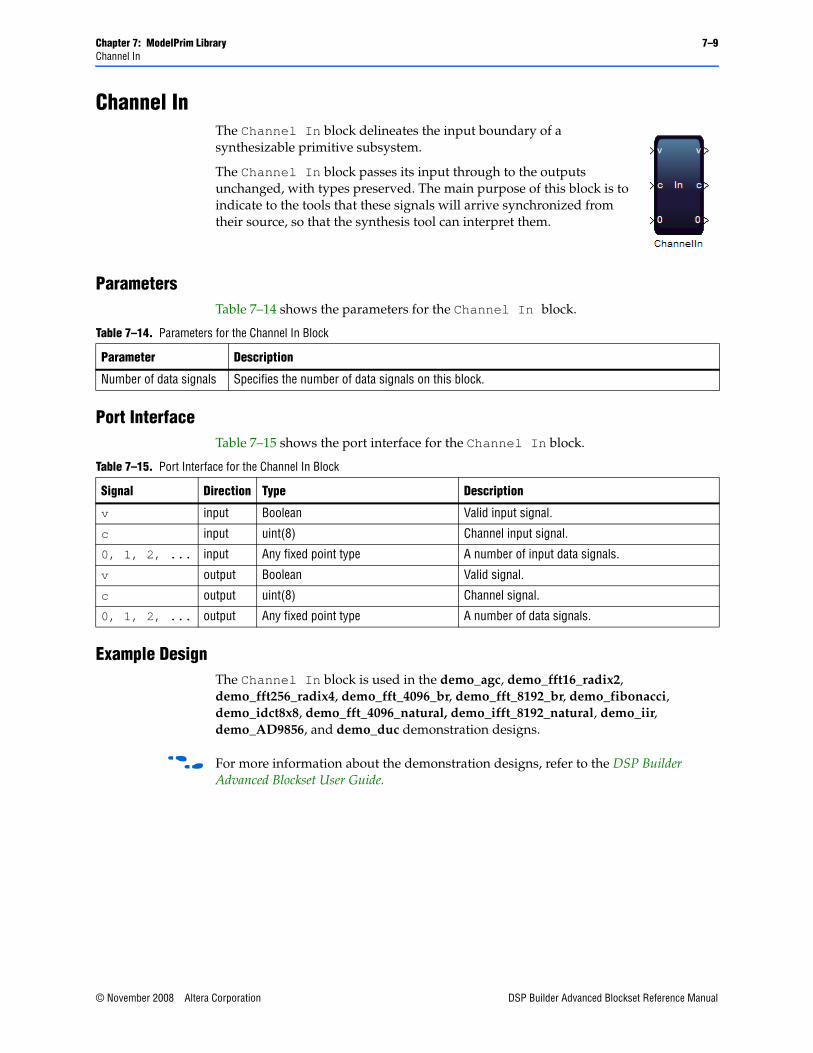
Chapter 7: ModelPrim Library 7–9Channel In
Channel InThe Channel In block delineates the input boundary of a synthesizable primitive subsystem.
The Channel In block passes its input through to the outputs unchanged, with types preserved. The main purpose of this block is to indicate to the tools that these signals will arrive synchronized from their source, so that the synthesis tool can interpret them.
ParametersTable 7–14 shows the parameters for the Channel In block.
Port InterfaceTable 7–15 shows the port interface for the Channel In block.
Example DesignThe Channel In block is used in the demo_agc, demo_fft16_radix2, demo_fft256_radix4, demo_fft_4096_br, demo_fft_8192_br, demo_fibonacci, demo_idct8x8, demo_fft_4096_natural, demo_ifft_8192_natural, demo_iir, demo_AD9856, and demo_duc demonstration designs.
f For more information about the demonstration designs, refer to the DSP Builder Advanced Blockset User Guide.
Table 7–14. Parameters for the Channel In Block
Parameter Description
Number of data signals Specifies the number of data signals on this block.
Table 7–15. Port Interface for the Channel In Block
Signal Direction Type Description
v input Boolean Valid input signal.
c input uint(8) Channel input signal.
0, 1, 2, ... input Any fixed point type A number of input data signals.
v output Boolean Valid signal.
c output uint(8) Channel signal.
0, 1, 2, ... output Any fixed point type A number of data signals.
© November 2008 Altera Corporation DSP Builder Advanced Blockset Reference Manual

7–10 Chapter 7: ModelPrim LibraryChannel Out
Channel OutThe Channel Out block delineates the output boundary of a synthesizable primitive subsystem.
The Channel Out block passes its input through to the outputs unchanged, with types preserved. The main purpose of this block is to indicate to the tools that these signals must be synchronized. The synthesis tool can ensure this.
After running a simulation in Simulink, the additional latency that is added to meet the specified timing constraints for the model is shown on the block. (Any delay explicitly added to the model, by for example a Sample Delay block, is not included in this latency.)
1 The value of the latency parameter can also be accessed by typing a command of the following form on the MATLAB command line:
get_param(gcb,’latency’)
ParametersTable 7–16 shows the parameters for the Channel Out block.
Port InterfaceTable 7–17 shows the port interface for the Channel Out block.
Example DesignThe Channel Out block is used in the demo_agc, demo_fft16_radix2, demo_fft256_radix4, demo_fft_4096_br, demo_fft_8192_br, demo_fibonacci, demo_idct8x8, demo_fft_4096_natural, demo_ifft_8192_natural, demo_iir, demo_AD9856, and demo_duc demonstration designs.
f For more information about the demonstration designs, refer to the DSP Builder Advanced Blockset User Guide.
Table 7–16. Parameters for the Channel Out Block
Parameter Description
Number of data signals Specifies the number of data signals on this block.
Table 7–17. Port Interface for the Channel Out Block
Signal Direction Type Description
v input Boolean Valid output signal.
c input uint(8) Channel output signal.
0, 1, 2, ... input Any fixed point type A number of output data signals.
v output Boolean Valid signal.
c output uint(8) Channel signal.
0, 1, 2, ... output Any fixed point type A number of data signals.
DSP Builder Advanced Blockset Reference Manual © November 2008 Altera Corporation
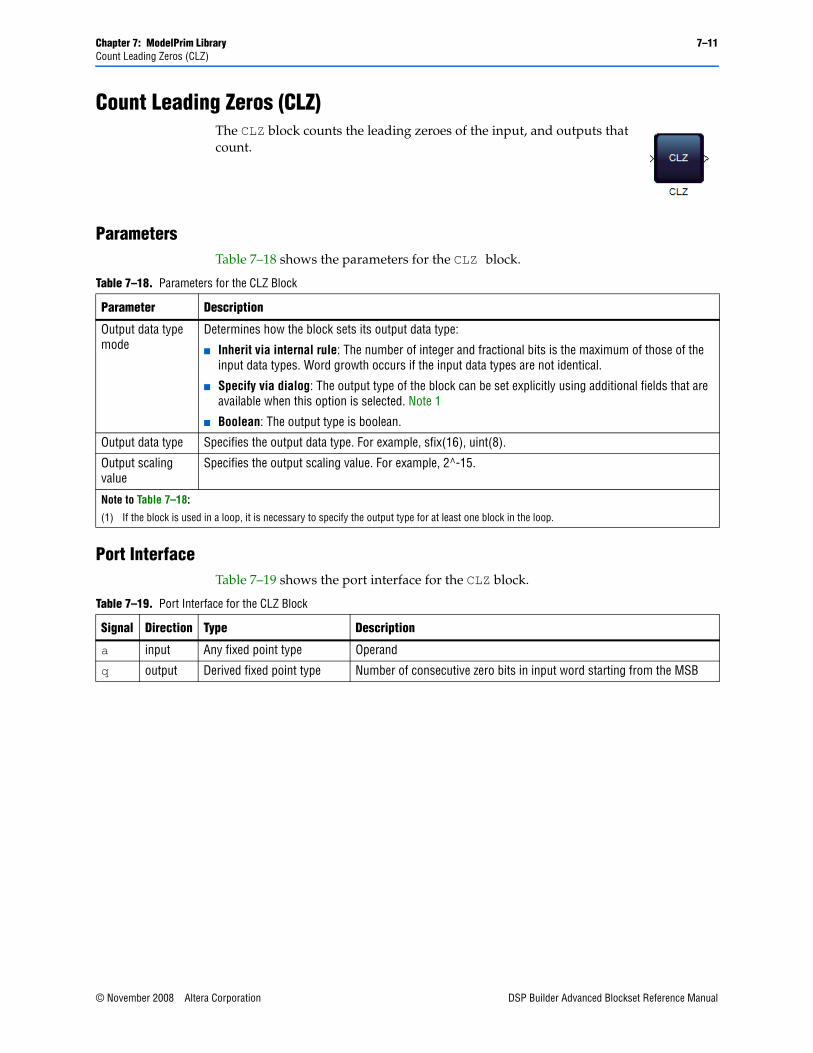
Chapter 7: ModelPrim Library 7–11Count Leading Zeros (CLZ)
Count Leading Zeros (CLZ)The CLZ block counts the leading zeroes of the input, and outputs that count.
ParametersTable 7–18 shows the parameters for the CLZ block.
Port InterfaceTable 7–19 shows the port interface for the CLZ block.
Table 7–18. Parameters for the CLZ Block
Parameter Description
Output data type mode
Determines how the block sets its output data type:
■ Inherit via internal rule: The number of integer and fractional bits is the maximum of those of the input data types. Word growth occurs if the input data types are not identical.
■ Specify via dialog: The output type of the block can be set explicitly using additional fields that are available when this option is selected. Note 1
■ Boolean: The output type is boolean.
Output data type Specifies the output data type. For example, sfix(16), uint(8).
Output scaling value
Specifies the output scaling value. For example, 2^-15.
Note to Table 7–18:
(1) If the block is used in a loop, it is necessary to specify the output type for at least one block in the loop.
Table 7–19. Port Interface for the CLZ Block
Signal Direction Type Description
a input Any fixed point type Operand
q output Derived fixed point type Number of consecutive zero bits in input word starting from the MSB
© November 2008 Altera Corporation DSP Builder Advanced Blockset Reference Manual
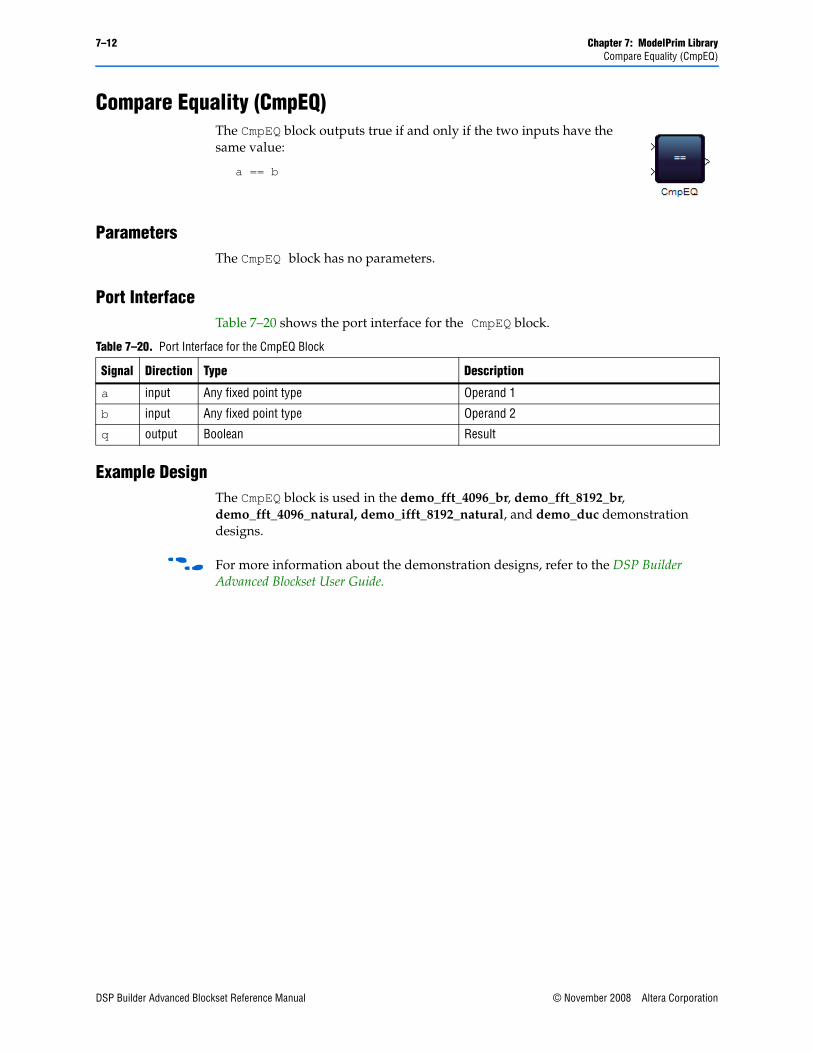
7–12 Chapter 7: ModelPrim LibraryCompare Equality (CmpEQ)
Compare Equality (CmpEQ)The CmpEQ block outputs true if and only if the two inputs have the same value:
a == b
ParametersThe CmpEQ block has no parameters.
Port InterfaceTable 7–20 shows the port interface for the CmpEQ block.
Example DesignThe CmpEQ block is used in the demo_fft_4096_br, demo_fft_8192_br, demo_fft_4096_natural, demo_ifft_8192_natural, and demo_duc demonstration designs.
f For more information about the demonstration designs, refer to the DSP Builder Advanced Blockset User Guide.
Table 7–20. Port Interface for the CmpEQ Block
Signal Direction Type Description
a input Any fixed point type Operand 1
b input Any fixed point type Operand 2
q output Boolean Result
DSP Builder Advanced Blockset Reference Manual © November 2008 Altera Corporation
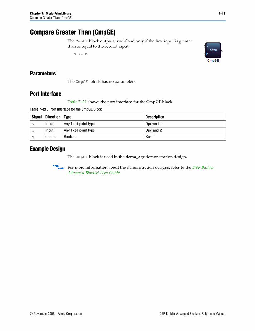
Chapter 7: ModelPrim Library 7–13Compare Greater Than (CmpGE)
Compare Greater Than (CmpGE)The CmpGE block outputs true if and only if the first input is greater than or equal to the second input:
a >= b
ParametersThe CmpGE block has no parameters.
Port InterfaceTable 7–21 shows the port interface for the CmpGE block.
Example DesignThe CmpGE block is used in the demo_agc demonstration design.
f For more information about the demonstration designs, refer to the DSP Builder Advanced Blockset User Guide.
Table 7–21. Port Interface for the CmpGE Block
Signal Direction Type Description
a input Any fixed point type Operand 1
b input Any fixed point type Operand 2
q output Boolean Result
© November 2008 Altera Corporation DSP Builder Advanced Blockset Reference Manual
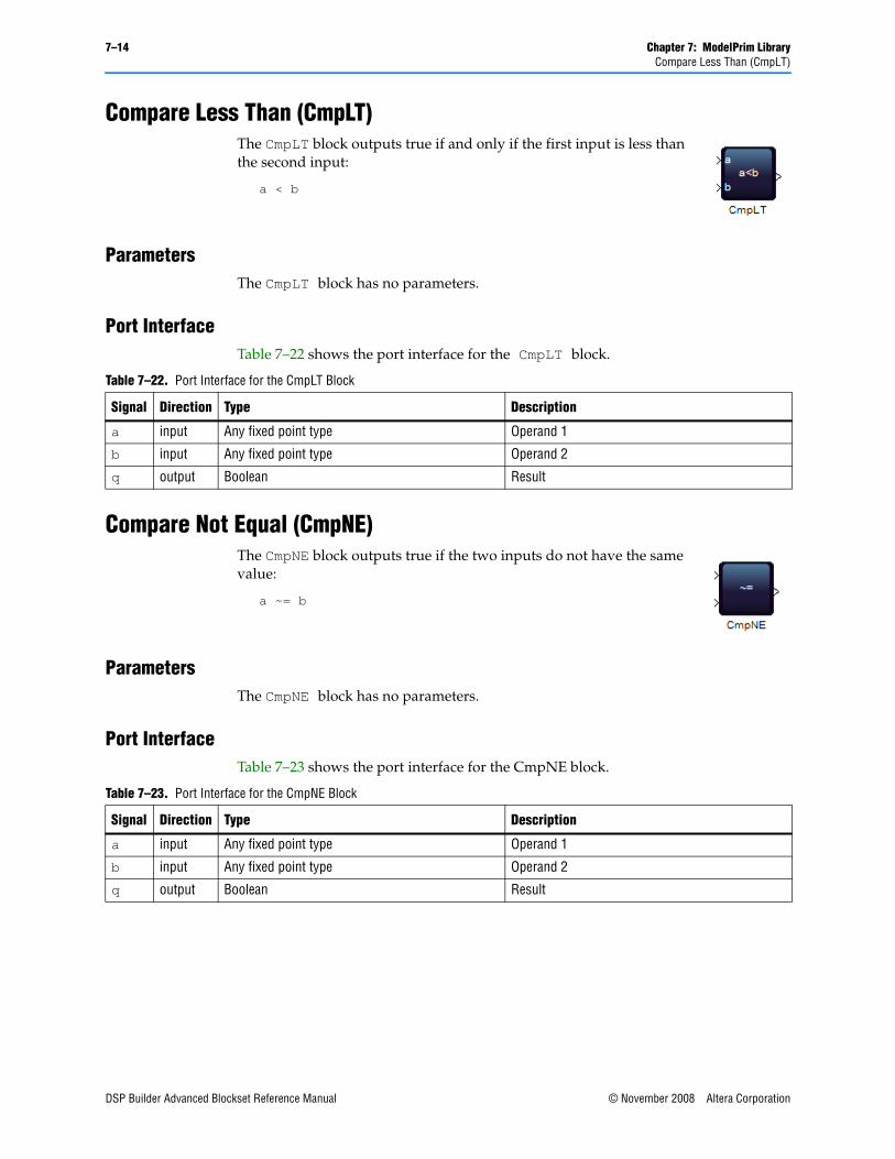
7–14 Chapter 7: ModelPrim LibraryCompare Less Than (CmpLT)
Compare Less Than (CmpLT)The CmpLT block outputs true if and only if the first input is less than the second input:
a < b
ParametersThe CmpLT block has no parameters.
Port InterfaceTable 7–22 shows the port interface for the CmpLT block.
Compare Not Equal (CmpNE)The CmpNE block outputs true if the two inputs do not have the same value:
a ~= b
ParametersThe CmpNE block has no parameters.
Port InterfaceTable 7–23 shows the port interface for the CmpNE block.
Table 7–22. Port Interface for the CmpLT Block
Signal Direction Type Description
a input Any fixed point type Operand 1
b input Any fixed point type Operand 2
q output Boolean Result
Table 7–23. Port Interface for the CmpNE Block
Signal Direction Type Description
a input Any fixed point type Operand 1
b input Any fixed point type Operand 2
q output Boolean Result
DSP Builder Advanced Blockset Reference Manual © November 2008 Altera Corporation

Chapter 7: ModelPrim Library 7–15Constant (Const)
Constant (Const)The Const block outputs a specified constant value.
ParametersTable 7–24 shows the parameters for the Const block.
Port InterfaceTable 7–25 shows the port interface for the Const block.
Example DesignThe Const block is used in the demo_fir_fractional, demo_regs, demo_agc, demo_filters_flow_control, demo_fft_4096_br, demo_fft_8192_br, demo_idct8x8, demo_fft_4096_natural, demo_ifft_8192_natural, demo_iir, demo_AD9856, demo_duc, and demo_wimax_duc demonstration designs.
f For more information about the demonstration designs, refer to the DSP Builder Advanced Blockset User Guide.
Table 7–24. Parameters for the Const Block
Parameter Description
Output data type mode
Determines how the block sets its output data type:
■ Inherit via internal rule: The number of integer and fractional bits is the maximum of those of the input data types. Word growth occurs if the input data types are not identical.
■ Specify via dialog: The output type of the block can be set explicitly using additional fields that are available when this option is selected. Note 1
■ Boolean: The output type is boolean.
Output data type Specifies the output data type. For example, sfix(16), uint(8).
Output scaling value
Specifies the output scaling value. For example, 2^-15.
Value Specifies the constant value.
Note to Table 7–24:
(1) If the block is used in a loop, it is necessary to specify the output type for at least one block in the loop.
Table 7–25. Port Interface for the Const Block
Signal Direction Type Description
q output Any fixed point type Constant value.
© November 2008 Altera Corporation DSP Builder Advanced Blockset Reference Manual
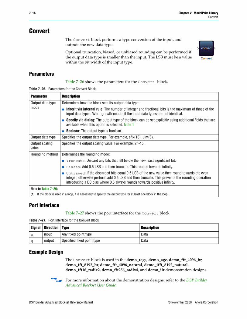
7–16 Chapter 7: ModelPrim LibraryConvert
ConvertThe Convert block performs a type conversion of the input, and outputs the new data type.
Optional truncation, biased, or unbiased rounding can be performed if the output data type is smaller than the input. The LSB must be a value within the bit width of the input type.
ParametersTable 7–26 shows the parameters for the Convert block.
Port InterfaceTable 7–27 shows the port interface for the Convert block.
Example DesignThe Convert block is used in the demo_regs, demo_agc, demo_fft_4096_br, demo_fft_8192_br, demo_fft_4096_natural, demo_ifft_8192_natural, demo_fft16_radix2, demo_fft256_radix4, and demo_iir demonstration designs.
f For more information about the demonstration designs, refer to the DSP Builder Advanced Blockset User Guide.
Table 7–26. Parameters for the Convert Block
Parameter Description
Output data type mode
Determines how the block sets its output data type:
■ Inherit via internal rule: The number of integer and fractional bits is the maximum of those of the input data types. Word growth occurs if the input data types are not identical.
■ Specify via dialog: The output type of the block can be set explicitly using additional fields that are available when this option is selected. Note 1
■ Boolean: The output type is boolean.
Output data type Specifies the output data type. For example, sfix(16), uint(8).
Output scaling value
Specifies the output scaling value. For example, 2^-15.
Rounding method Determines the rounding mode:
■ Truncate: Discard any bits that fall below the new least significant bit.
■ Biased: Add 0.5 LSB and then truncate. This rounds towards infinity.
■ Unbiased: If the discarded bits equal 0.5 LSB of the new value then round towards the even integer, otherwise perform add 0.5 LSB and then truncate. This prevents the rounding operation introducing a DC bias where 0.5 always rounds towards positive infinity.
Note to Table 7–26:
(1) If the block is used in a loop, it is necessary to specify the output type for at least one block in the loop.
Table 7–27. Port Interface for the Convert Block
Signal Direction Type Description
a input Any fixed point type Data
q output Specified fixed point type Data
DSP Builder Advanced Blockset Reference Manual © November 2008 Altera Corporation
Chapter 7: ModelPrim Library 7–17CORDIC
CORDICThe CORDIC block performs a coordinate rotation using the coordinate rotation digital computer algorithm.
The CORDIC algorithm is a is a simple and efficient algorithm to calculate hyperbolic and trigonometric functions. It calculates the trigonometric functions of sine, cosine, magnitude and phase (arctangent) to any desired precision. It is commonly used when no hardware multiplier is desired as the only operations it requires are addition, subtraction, bit shift and table-lookup.
The CORDIC algorithm is generally faster than other approaches when use of a hardware multiplier is to be avoided, or when the number of gates required to implement the functions it supports should be minimized. Alternatively, when a hardware multiplier is available, table-lookup and power series methods are generally faster than CORDIC.
CORDIC is based on rotating the phase of a complex number, by multiplying it by a succession of constant values. The multiplications can all be powers of 2, and can be done using just shifts and adds in binary arithmetic. Therefore no actual multiplier function is needed.
During each multiplication, a gain occurs equal to:
where i represents the ith iterative step.
The total gain of the successive multiplications has a value of:
where n is the number of iterations.
This total gain can be calculated in advance and stored in a table. Additionally, it can be noted that:
The CORDIC block implements the these iterative steps using a set of shift-add algorithms to perform a coordinate rotation.
The CORDIC block takes four inputs, where the x and y inputs represent the (x, y) coordinates of the input vector, the p input represents the angle input, and the v represents the mode of the CORDIC block. It currently supports two modes:
■ The first mode rotates the input vector by a specified angle.
■ The second mode rotates the input vector to the x-axis while recording the angle required to make that rotation.
Ki 1 2 2 i–+=
K n( ) Ki
i 0=
n 1–
∏ 1 2 2 i–+
i 0=
n 1–
∏= =
K K n( )n ∞→lim 1.64676≈=
© November 2008 Altera Corporation DSP Builder Advanced Blockset Reference Manual
7–18 Chapter 7: ModelPrim LibraryCORDIC
The x, y inputs must have the same bit width. The number of stages (iterations) inside the CORDIC block is determined by the input bit width of the x, y inputs, unless you explicitly specify an output bit width smaller than the input bit width in the block parameters.
The CORDIC gain is completely ignored to save time and resource. The bit width of x, y inputs automatically grows by two bits inside the CORDIC block to account for the gaining factor of the CORDIC algorithm. Hence the x, y outputs are two bits wider than the input and you need to handle the extra two bits in your design, if no output bit width is specified explicitly through the block parameters. The CORDIC gain can be compensated for outside the CORDIC block.
The p input is the angular value and has a range between –π and +π, which requires at least three integer bits to fully represent the range. The v input determines the mode. You can trade-off between accuracy for size (and efficiency) by specifying a smaller output data width to reduce the number of stages inside the CORDIC block.
ParametersTable 7–28 shows the parameters for the CORDIC block.
Port InterfaceTable 7–29 shows the port interface for the CORDIC block.
Table 7–28. Parameters for the CORDIC Block
Parameter Description
Output data type mode
Determines how the block sets its output data type:
■ Inherit via internal rule: The number of integer and fractional bits is the maximum of those of the input data types. Word growth occurs if the input data types are not identical.
■ Specify via dialog: The output type of the block can be set explicitly using additional fields that are available when this option is selected. Note 1
■ Boolean: The output type is boolean.
Output data type Specifies the output data type. For example, sfix(16), uint(8).
Output scaling value Specifies the output scaling value. For example, 2^-15.
Note to Table 7–28:
(1) If the block is used in a loop, it is necessary to specify the output type for at least one block in the loop.
Table 7–29. Port Interface for the CORDIC Block
Signal Direction Type Description
x input Any fixed point type x coordinate of the input vector.
y input Any fixed point type y coordinate of the input vector.
p input Any fixed point type Required angle of rotation in the range -pi to pi.
v input Any fixed point type Selects the mode of operation (0 = rotate by angle, 1 = rotate to x-axis).
x output Any fixed point type x coordinate of the output vector.
y output Any fixed point type y coordinate of the output vector.
p output Any fixed point type Angle through which the coordinates were rotated.
DSP Builder Advanced Blockset Reference Manual © November 2008 Altera Corporation
Chapter 7: ModelPrim Library 7–19Counter
CounterThe Counter block maintains a counter and outputs the value each cycle.
The input is a counter enable and allows irregular counters to be implemented. The counter is initialized to the value provided, and counts with the given modulo, with the step size provided.
count = _initial_value;
while (1) { if (en) count = (count + _step_size) % _modulo}
ParametersTable 7–30 shows the parameters for the Counter block.
Port InterfaceTable 7–31 shows the port interface for the Counter block.
Example DesignThe Counter block is used in the demo_fft16_radix2, demo_fft256_radix4, demo_fft_4096_br, demo_fft_8192_br, demo_fft_4096_natural, demo_ifft_8192_natural, and helloWorld demonstration designs.
f For more information about the demonstration designs, refer to the DSP Builder Advanced Blockset User Guide.
Table 7–30. Parameters for the Counter Block
Parameter Description
Output data type mode
Determines how the block sets its output data type:
■ Inherit via internal rule: The number of integer and fractional bits is the maximum of those of the input data types. Word growth occurs if the input data types are not identical.
■ Specify via dialog: The output type of the block can be set explicitly using additional fields that are available when this option is selected. Note 1
■ Boolean: The output type is boolean.
Output data type Specifies the output data type. For example, sfix(16), uint(8).
Output scaling value
Specifies the output scaling value. For example, 2^-15.
Counter setup A vector that specifies the counter in the format:
[<initial_value> <modulo> <step size>]
For example, [0 32 1]
Note to Table 7–30:
(1) If the block is used in a loop, it is necessary to specify the output type for at least one block in the loop.
Table 7–31. Port Interface for the Counter Block
Signal Direction Type Description
en input Boolean Count enable
q output Specified fixed point type Result
© November 2008 Altera Corporation DSP Builder Advanced Blockset Reference Manual
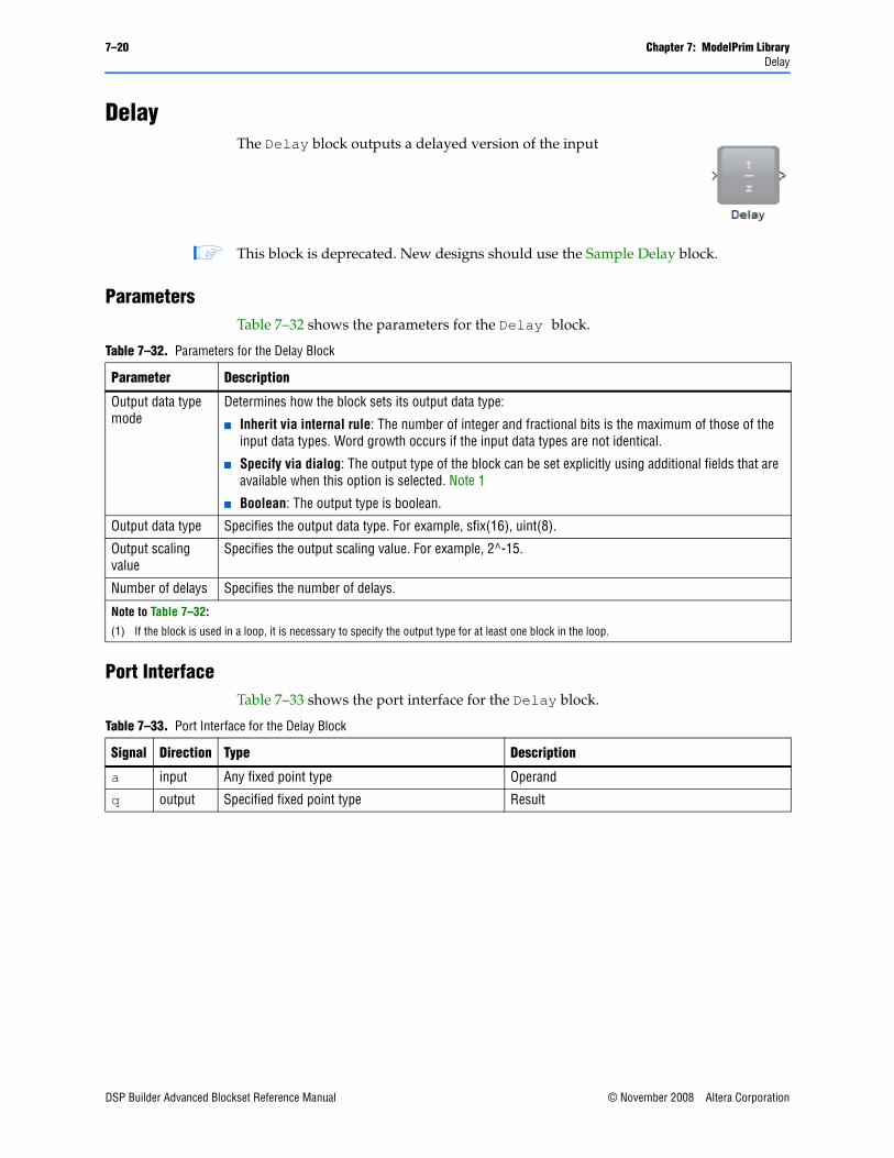
7–20 Chapter 7: ModelPrim LibraryDelay
DelayThe Delay block outputs a delayed version of the input
1 This block is deprecated. New designs should use the Sample Delay block.
ParametersTable 7–32 shows the parameters for the Delay block.
Port InterfaceTable 7–33 shows the port interface for the Delay block.
Table 7–32. Parameters for the Delay Block
Parameter Description
Output data type mode
Determines how the block sets its output data type:
■ Inherit via internal rule: The number of integer and fractional bits is the maximum of those of the input data types. Word growth occurs if the input data types are not identical.
■ Specify via dialog: The output type of the block can be set explicitly using additional fields that are available when this option is selected. Note 1
■ Boolean: The output type is boolean.
Output data type Specifies the output data type. For example, sfix(16), uint(8).
Output scaling value
Specifies the output scaling value. For example, 2^-15.
Number of delays Specifies the number of delays.
Note to Table 7–32:
(1) If the block is used in a loop, it is necessary to specify the output type for at least one block in the loop.
Table 7–33. Port Interface for the Delay Block
Signal Direction Type Description
a input Any fixed point type Operand
q output Specified fixed point type Result
DSP Builder Advanced Blockset Reference Manual © November 2008 Altera Corporation
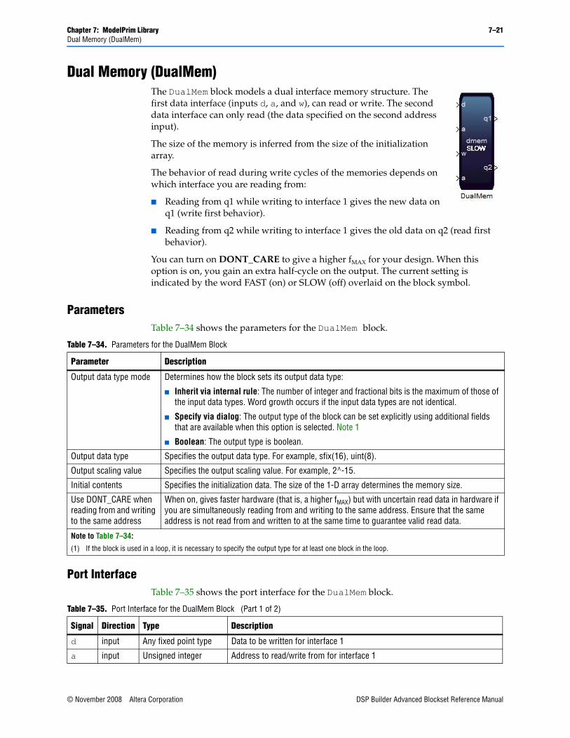
Chapter 7: ModelPrim Library 7–21Dual Memory (DualMem)
Dual Memory (DualMem)The DualMem block models a dual interface memory structure. The first data interface (inputs d, a, and w), can read or write. The second data interface can only read (the data specified on the second address input).
The size of the memory is inferred from the size of the initialization array.
The behavior of read during write cycles of the memories depends on which interface you are reading from:
■ Reading from q1 while writing to interface 1 gives the new data on q1 (write first behavior).
■ Reading from q2 while writing to interface 1 gives the old data on q2 (read first behavior).
You can turn on DONT_CARE to give a higher fMAX for your design. When this option is on, you gain an extra half-cycle on the output. The current setting is indicated by the word FAST (on) or SLOW (off) overlaid on the block symbol.
ParametersTable 7–34 shows the parameters for the DualMem block.
Port InterfaceTable 7–35 shows the port interface for the DualMem block.
Table 7–34. Parameters for the DualMem Block
Parameter Description
Output data type mode Determines how the block sets its output data type:
■ Inherit via internal rule: The number of integer and fractional bits is the maximum of those of the input data types. Word growth occurs if the input data types are not identical.
■ Specify via dialog: The output type of the block can be set explicitly using additional fields that are available when this option is selected. Note 1
■ Boolean: The output type is boolean.
Output data type Specifies the output data type. For example, sfix(16), uint(8).
Output scaling value Specifies the output scaling value. For example, 2^-15.
Initial contents Specifies the initialization data. The size of the 1-D array determines the memory size.
Use DONT_CARE when reading from and writing to the same address
When on, gives faster hardware (that is, a higher fMAX) but with uncertain read data in hardware if you are simultaneously reading from and writing to the same address. Ensure that the same address is not read from and written to at the same time to guarantee valid read data.
Note to Table 7–34:
(1) If the block is used in a loop, it is necessary to specify the output type for at least one block in the loop.
Table 7–35. Port Interface for the DualMem Block (Part 1 of 2)
Signal Direction Type Description
d input Any fixed point type Data to be written for interface 1
a input Unsigned integer Address to read/write from for interface 1
© November 2008 Altera Corporation DSP Builder Advanced Blockset Reference Manual
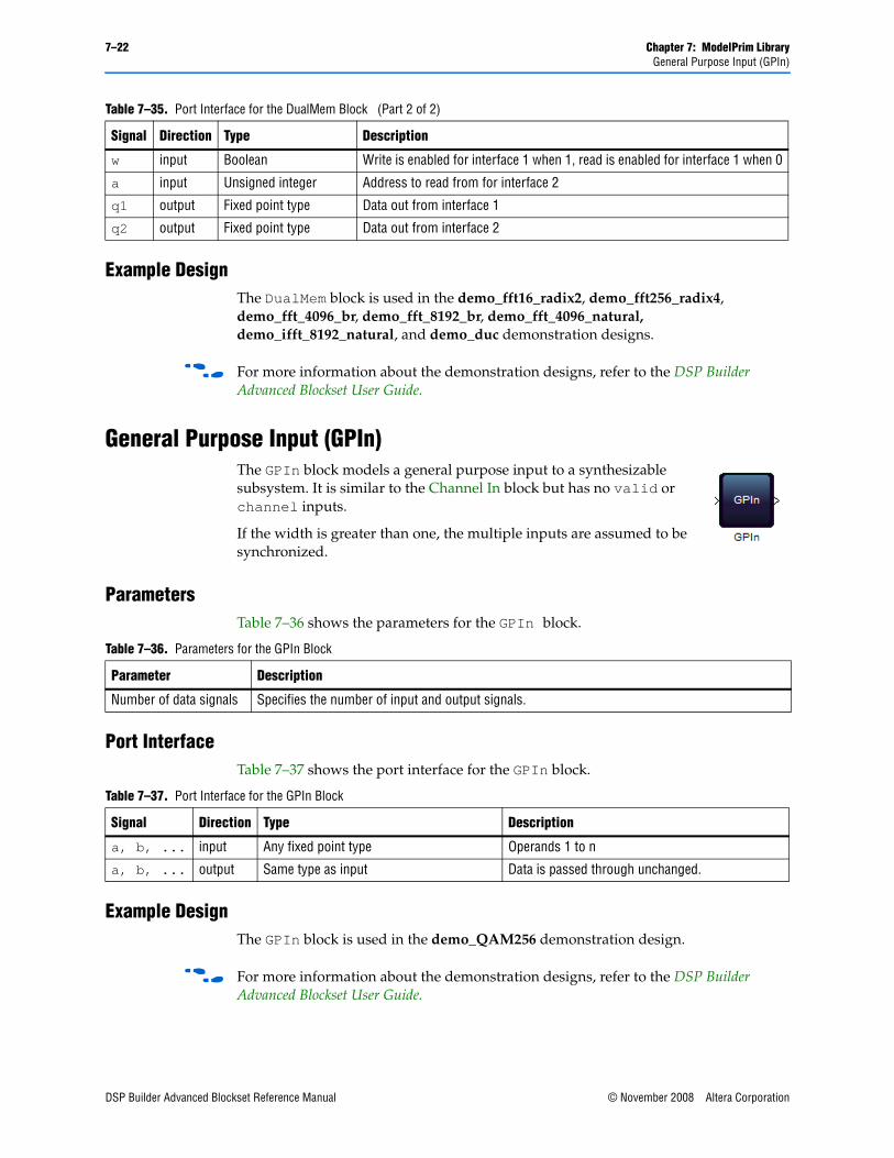
7–22 Chapter 7: ModelPrim LibraryGeneral Purpose Input (GPIn)
Example DesignThe DualMem block is used in the demo_fft16_radix2, demo_fft256_radix4, demo_fft_4096_br, demo_fft_8192_br, demo_fft_4096_natural, demo_ifft_8192_natural, and demo_duc demonstration designs.
f For more information about the demonstration designs, refer to the DSP Builder Advanced Blockset User Guide.
General Purpose Input (GPIn)The GPIn block models a general purpose input to a synthesizable subsystem. It is similar to the Channel In block but has no valid or channel inputs.
If the width is greater than one, the multiple inputs are assumed to be synchronized.
ParametersTable 7–36 shows the parameters for the GPIn block.
Port InterfaceTable 7–37 shows the port interface for the GPIn block.
Example DesignThe GPIn block is used in the demo_QAM256 demonstration design.
f For more information about the demonstration designs, refer to the DSP Builder Advanced Blockset User Guide.
w input Boolean Write is enabled for interface 1 when 1, read is enabled for interface 1 when 0
a input Unsigned integer Address to read from for interface 2
q1 output Fixed point type Data out from interface 1
q2 output Fixed point type Data out from interface 2
Table 7–35. Port Interface for the DualMem Block (Part 2 of 2)
Signal Direction Type Description
Table 7–36. Parameters for the GPIn Block
Parameter Description
Number of data signals Specifies the number of input and output signals.
Table 7–37. Port Interface for the GPIn Block
Signal Direction Type Description
a, b, ... input Any fixed point type Operands 1 to n
a, b, ... output Same type as input Data is passed through unchanged.
DSP Builder Advanced Blockset Reference Manual © November 2008 Altera Corporation
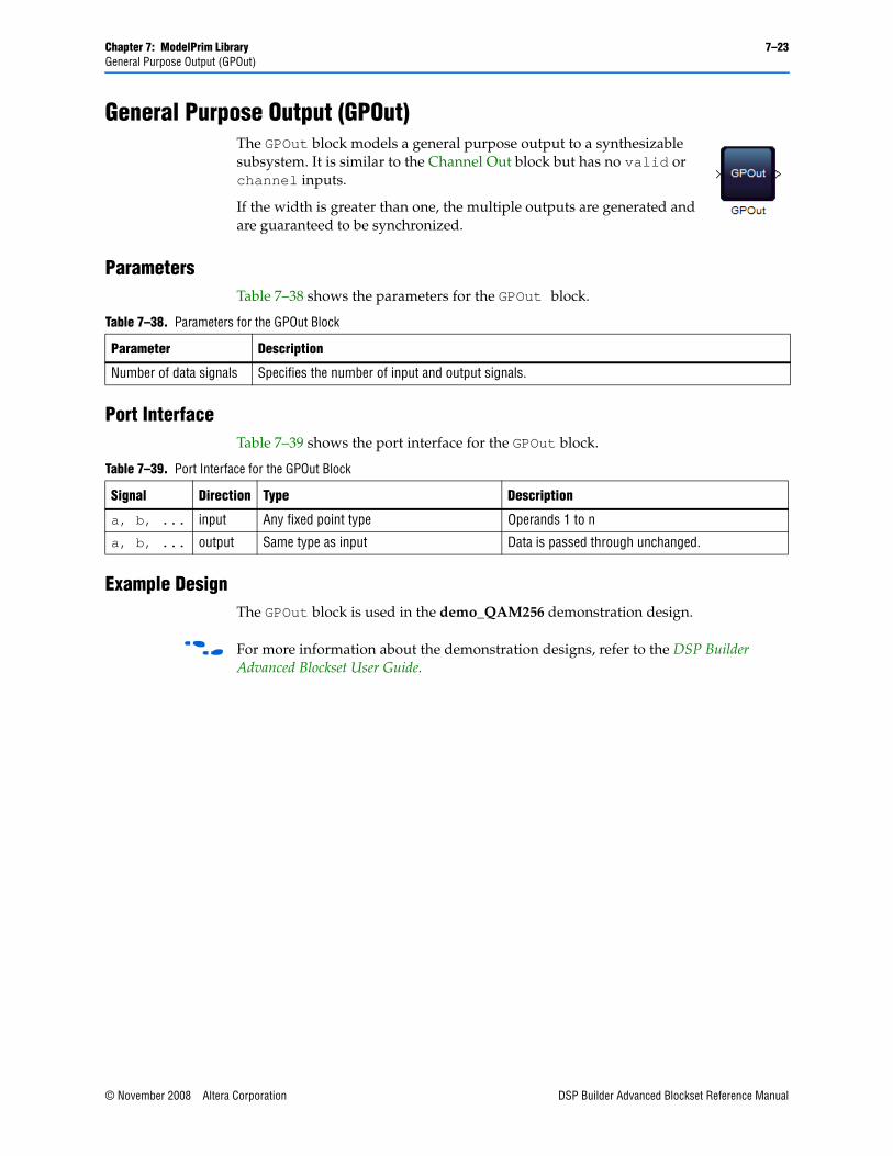
Chapter 7: ModelPrim Library 7–23General Purpose Output (GPOut)
General Purpose Output (GPOut)The GPOut block models a general purpose output to a synthesizable subsystem. It is similar to the Channel Out block but has no valid or channel inputs.
If the width is greater than one, the multiple outputs are generated and are guaranteed to be synchronized.
ParametersTable 7–38 shows the parameters for the GPOut block.
Port InterfaceTable 7–39 shows the port interface for the GPOut block.
Example DesignThe GPOut block is used in the demo_QAM256 demonstration design.
f For more information about the demonstration designs, refer to the DSP Builder Advanced Blockset User Guide.
Table 7–38. Parameters for the GPOut Block
Parameter Description
Number of data signals Specifies the number of input and output signals.
Table 7–39. Port Interface for the GPOut Block
Signal Direction Type Description
a, b, ... input Any fixed point type Operands 1 to n
a, b, ... output Same type as input Data is passed through unchanged.
© November 2008 Altera Corporation DSP Builder Advanced Blockset Reference Manual
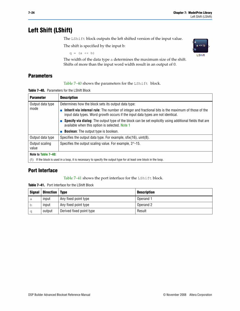
7–24 Chapter 7: ModelPrim LibraryLeft Shift (LShift)
Left Shift (LShift)The LShift block outputs the left shifted version of the input value.
The shift is specified by the input b:
q = (a << b)
The width of the data type a determines the maximum size of the shift. Shifts of more than the input word width result in an output of 0.
ParametersTable 7–40 shows the parameters for the LShift block.
Port InterfaceTable 7–41 shows the port interface for the LShift block.
Table 7–40. Parameters for the LShift Block
Parameter Description
Output data type mode
Determines how the block sets its output data type:
■ Inherit via internal rule: The number of integer and fractional bits is the maximum of those of the input data types. Word growth occurs if the input data types are not identical.
■ Specify via dialog: The output type of the block can be set explicitly using additional fields that are available when this option is selected. Note 1
■ Boolean: The output type is boolean.
Output data type Specifies the output data type. For example, sfix(16), uint(8).
Output scaling value
Specifies the output scaling value. For example, 2^-15.
Note to Table 7–40:
(1) If the block is used in a loop, it is necessary to specify the output type for at least one block in the loop.
Table 7–41. Port Interface for the LShift Block
Signal Direction Type Description
a input Any fixed point type Operand 1
b input Any fixed point type Operand 2
q output Derived fixed point type Result
DSP Builder Advanced Blockset Reference Manual © November 2008 Altera Corporation
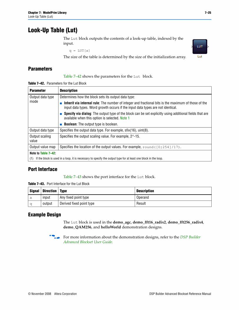
Chapter 7: ModelPrim Library 7–25Look-Up Table (Lut)
Look-Up Table (Lut)The Lut block outputs the contents of a look-up table, indexed by the input.
q = LUT[a]
The size of the table is determined by the size of the initialization array.
ParametersTable 7–42 shows the parameters for the Lut block.
Port InterfaceTable 7–43 shows the port interface for the Lut block.
Example DesignThe Lut block is used in the demo_agc, demo_fft16_radix2, demo_fft256_radix4, demo_QAM256, and helloWorld demonstration designs.
f For more information about the demonstration designs, refer to the DSP Builder Advanced Blockset User Guide.
Table 7–42. Parameters for the Lut Block
Parameter Description
Output data type mode
Determines how the block sets its output data type:
■ Inherit via internal rule: The number of integer and fractional bits is the maximum of those of the input data types. Word growth occurs if the input data types are not identical.
■ Specify via dialog: The output type of the block can be set explicitly using additional fields that are available when this option is selected. Note 1
■ Boolean: The output type is boolean.
Output data type Specifies the output data type. For example, sfix(16), uint(8).
Output scaling value
Specifies the output scaling value. For example, 2^-15.
Output value map Specifies the location of the output values. For example, round([0;254]/17).
Note to Table 7–42:
(1) If the block is used in a loop, it is necessary to specify the output type for at least one block in the loop.
Table 7–43. Port Interface for the Lut Block
Signal Direction Type Description
a input Any fixed point type Operand
q output Derived fixed point type Result
© November 2008 Altera Corporation DSP Builder Advanced Blockset Reference Manual
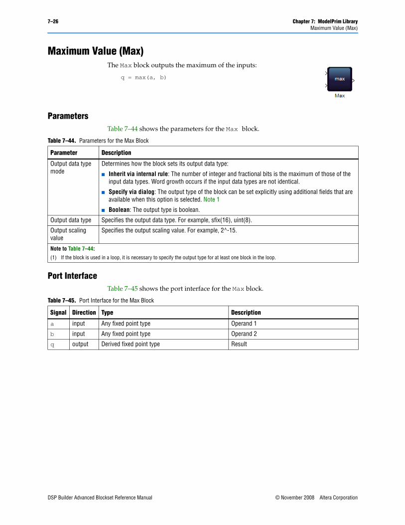
7–26 Chapter 7: ModelPrim LibraryMaximum Value (Max)
Maximum Value (Max)The Max block outputs the maximum of the inputs:
q = max(a, b)
ParametersTable 7–44 shows the parameters for the Max block.
Port InterfaceTable 7–45 shows the port interface for the Max block.
Table 7–44. Parameters for the Max Block
Parameter Description
Output data type mode
Determines how the block sets its output data type:
■ Inherit via internal rule: The number of integer and fractional bits is the maximum of those of the input data types. Word growth occurs if the input data types are not identical.
■ Specify via dialog: The output type of the block can be set explicitly using additional fields that are available when this option is selected. Note 1
■ Boolean: The output type is boolean.
Output data type Specifies the output data type. For example, sfix(16), uint(8).
Output scaling value
Specifies the output scaling value. For example, 2^-15.
Note to Table 7–44:
(1) If the block is used in a loop, it is necessary to specify the output type for at least one block in the loop.
Table 7–45. Port Interface for the Max Block
Signal Direction Type Description
a input Any fixed point type Operand 1
b input Any fixed point type Operand 2
q output Derived fixed point type Result
DSP Builder Advanced Blockset Reference Manual © November 2008 Altera Corporation
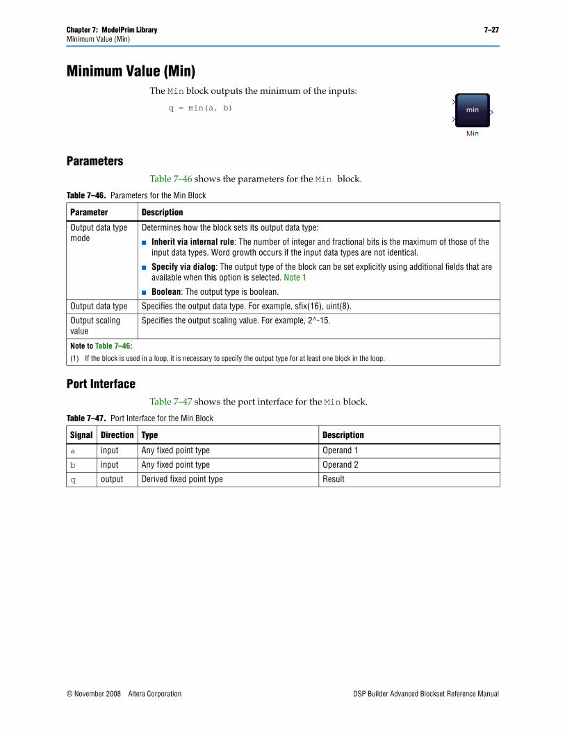
Chapter 7: ModelPrim Library 7–27Minimum Value (Min)
Minimum Value (Min)The Min block outputs the minimum of the inputs:
q = min(a, b)
ParametersTable 7–46 shows the parameters for the Min block.
Port InterfaceTable 7–47 shows the port interface for the Min block.
Table 7–46. Parameters for the Min Block
Parameter Description
Output data type mode
Determines how the block sets its output data type:
■ Inherit via internal rule: The number of integer and fractional bits is the maximum of those of the input data types. Word growth occurs if the input data types are not identical.
■ Specify via dialog: The output type of the block can be set explicitly using additional fields that are available when this option is selected. Note 1
■ Boolean: The output type is boolean.
Output data type Specifies the output data type. For example, sfix(16), uint(8).
Output scaling value
Specifies the output scaling value. For example, 2^-15.
Note to Table 7–46:
(1) If the block is used in a loop, it is necessary to specify the output type for at least one block in the loop.
Table 7–47. Port Interface for the Min Block
Signal Direction Type Description
a input Any fixed point type Operand 1
b input Any fixed point type Operand 2
q output Derived fixed point type Result
© November 2008 Altera Corporation DSP Builder Advanced Blockset Reference Manual

7–28 Chapter 7: ModelPrim LibraryMultiply (Mult)
Multiply (Mult)The Mult block outputs the product of the inputs:
q = a × b
ParametersTable 7–48 shows the parameters for the Mult block.
Port InterfaceTable 7–49 shows the port interface for the Mult block.
Example DesignThe Mult block is used in the demo_regs, demo_agc, demo_idct8x8, demo_iir, demo_AD9856, and demo_duc demonstration designs.
f For more information about the demonstration designs, refer to the DSP Builder Advanced Blockset User Guide.
Table 7–48. Parameters for the Mult Block
Parameter Description
Output data type mode
Determines how the block sets its output data type:
■ Inherit via internal rule: The number of integer and fractional bits is the maximum of those of the input data types. Word growth occurs if the input data types are not identical.
■ Specify via dialog: The output type of the block can be set explicitly using additional fields that are available when this option is selected. Note 1
■ Boolean: The output type is boolean.
Output data type Specifies the output data type. For example, sfix(16), uint(8).
Output scaling value
Specifies the output scaling value. For example, 2^-15.
Note to Table 7–48:
(1) If the block is used in a loop, it is necessary to specify the output type for at least one block in the loop.
Table 7–49. Port Interface for the Mult Block
Signal Direction Type Description
a input Any fixed point type Operand 1
b input Any fixed point type Operand 2
q output Derived fixed point type Result
DSP Builder Advanced Blockset Reference Manual © November 2008 Altera Corporation
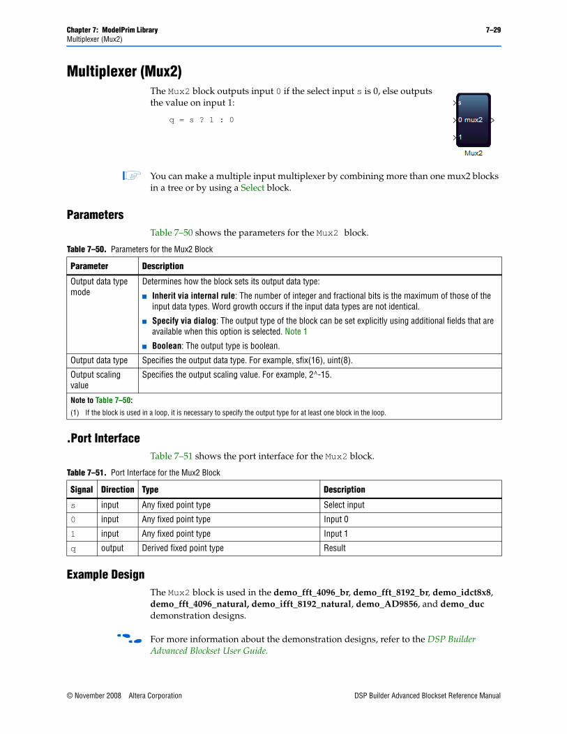
Chapter 7: ModelPrim Library 7–29Multiplexer (Mux2)
Multiplexer (Mux2)The Mux2 block outputs input 0 if the select input s is 0, else outputs the value on input 1:
q = s ? 1 : 0
1 You can make a multiple input multiplexer by combining more than one mux2 blocks in a tree or by using a Select block.
ParametersTable 7–50 shows the parameters for the Mux2 block.
.Port InterfaceTable 7–51 shows the port interface for the Mux2 block.
Example DesignThe Mux2 block is used in the demo_fft_4096_br, demo_fft_8192_br, demo_idct8x8, demo_fft_4096_natural, demo_ifft_8192_natural, demo_AD9856, and demo_duc demonstration designs.
f For more information about the demonstration designs, refer to the DSP Builder Advanced Blockset User Guide.
Table 7–50. Parameters for the Mux2 Block
Parameter Description
Output data type mode
Determines how the block sets its output data type:
■ Inherit via internal rule: The number of integer and fractional bits is the maximum of those of the input data types. Word growth occurs if the input data types are not identical.
■ Specify via dialog: The output type of the block can be set explicitly using additional fields that are available when this option is selected. Note 1
■ Boolean: The output type is boolean.
Output data type Specifies the output data type. For example, sfix(16), uint(8).
Output scaling value
Specifies the output scaling value. For example, 2^-15.
Note to Table 7–50:
(1) If the block is used in a loop, it is necessary to specify the output type for at least one block in the loop.
Table 7–51. Port Interface for the Mux2 Block
Signal Direction Type Description
s input Any fixed point type Select input
0 input Any fixed point type Input 0
1 input Any fixed point type Input 1
q output Derived fixed point type Result
© November 2008 Altera Corporation DSP Builder Advanced Blockset Reference Manual

7–30 Chapter 7: ModelPrim LibraryNAND Gate (Nand)
NAND Gate (Nand)The Nand block outputs the logical NAND of the input values:
q = ~(a & b)
If the number of inputs is set to 1, then output the logical NAND of all the individual bits of the input word.
ParametersTable 7–52 shows the parameters for the Nand block.
Port InterfaceTable 7–52 shows the port interface for the Nand block.
Table 7–52. Parameters for the Nand Block
Parameter Description
Number of inputs Specifies the number of inputs.
Output data type mode
Determines how the block sets its output data type:
■ Inherit via internal rule: The number of integer and fractional bits is the maximum of those of the input data types. Word growth occurs if the input data types are not identical.
■ Specify via dialog: The output type of the block can be set explicitly using additional fields that are available when this option is selected. Note 1
■ Boolean: The output type is boolean.
Output data type Specifies the output data type. For example, sfix(16), uint(8).
Output scaling value
Specifies the output scaling value. For example, 2^-15.
Note to Table 7–52:
(1) If the block is used in a loop, it is necessary to specify the output type for at least one block in the loop.
Table 7–53. Port Interface for the Nand Block
Signal Direction Type Description
a input Any fixed point type Operand 1
b input Any fixed point type Operand 2
q output Derived fixed point type Result
DSP Builder Advanced Blockset Reference Manual © November 2008 Altera Corporation
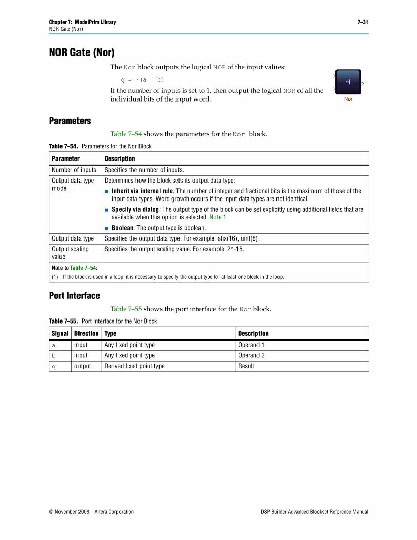
Chapter 7: ModelPrim Library 7–31NOR Gate (Nor)
NOR Gate (Nor)The Nor block outputs the logical NOR of the input values:
q = ~(a | b)
If the number of inputs is set to 1, then output the logical NOR of all the individual bits of the input word.
ParametersTable 7–54 shows the parameters for the Nor block.
Port InterfaceTable 7–55 shows the port interface for the Nor block.
Table 7–54. Parameters for the Nor Block
Parameter Description
Number of inputs Specifies the number of inputs.
Output data type mode
Determines how the block sets its output data type:
■ Inherit via internal rule: The number of integer and fractional bits is the maximum of those of the input data types. Word growth occurs if the input data types are not identical.
■ Specify via dialog: The output type of the block can be set explicitly using additional fields that are available when this option is selected. Note 1
■ Boolean: The output type is boolean.
Output data type Specifies the output data type. For example, sfix(16), uint(8).
Output scaling value
Specifies the output scaling value. For example, 2^-15.
Note to Table 7–54:
(1) If the block is used in a loop, it is necessary to specify the output type for at least one block in the loop.
Table 7–55. Port Interface for the Nor Block
Signal Direction Type Description
a input Any fixed point type Operand 1
b input Any fixed point type Operand 2
q output Derived fixed point type Result
© November 2008 Altera Corporation DSP Builder Advanced Blockset Reference Manual
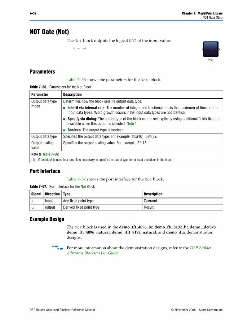
7–32 Chapter 7: ModelPrim LibraryNOT Gate (Not)
NOT Gate (Not)The Not block outputs the logical NOT of the input value:
q = ~a
ParametersTable 7–56 shows the parameters for the Not block.
Port InterfaceTable 7–57 shows the port interface for the Not block.
Example DesignThe Not block is used in the demo_fft_4096_br, demo_fft_8192_br, demo_idct8x8, demo_fft_4096_natural, demo_ifft_8192_natural, and demo_duc demonstration designs.
f For more information about the demonstration designs, refer to the DSP Builder Advanced Blockset User Guide.
Table 7–56. Parameters for the Not Block
Parameter Description
Output data type mode
Determines how the block sets its output data type:
■ Inherit via internal rule: The number of integer and fractional bits is the maximum of those of the input data types. Word growth occurs if the input data types are not identical.
■ Specify via dialog: The output type of the block can be set explicitly using additional fields that are available when this option is selected. Note 1
■ Boolean: The output type is boolean.
Output data type Specifies the output data type. For example, sfix(16), uint(8).
Output scaling value
Specifies the output scaling value. For example, 2^-15.
Note to Table 7–56:
(1) If the block is used in a loop, it is necessary to specify the output type for at least one block in the loop.
Table 7–57. Port Interface for the Not Block
Signal Direction Type Description
a input Any fixed point type Operand
q output Derived fixed point type Result
DSP Builder Advanced Blockset Reference Manual © November 2008 Altera Corporation
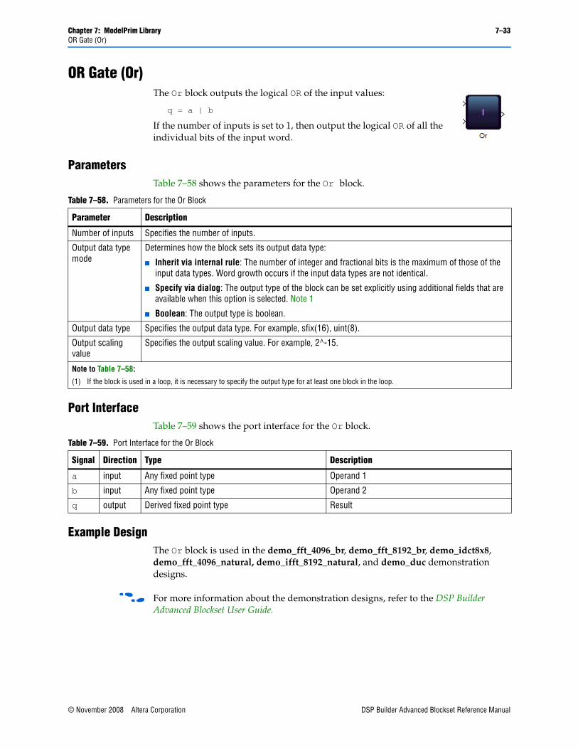
Chapter 7: ModelPrim Library 7–33OR Gate (Or)
OR Gate (Or)The Or block outputs the logical OR of the input values:
q = a | b
If the number of inputs is set to 1, then output the logical OR of all the individual bits of the input word.
ParametersTable 7–58 shows the parameters for the Or block.
Port InterfaceTable 7–59 shows the port interface for the Or block.
Example DesignThe Or block is used in the demo_fft_4096_br, demo_fft_8192_br, demo_idct8x8, demo_fft_4096_natural, demo_ifft_8192_natural, and demo_duc demonstration designs.
f For more information about the demonstration designs, refer to the DSP Builder Advanced Blockset User Guide.
Table 7–58. Parameters for the Or Block
Parameter Description
Number of inputs Specifies the number of inputs.
Output data type mode
Determines how the block sets its output data type:
■ Inherit via internal rule: The number of integer and fractional bits is the maximum of those of the input data types. Word growth occurs if the input data types are not identical.
■ Specify via dialog: The output type of the block can be set explicitly using additional fields that are available when this option is selected. Note 1
■ Boolean: The output type is boolean.
Output data type Specifies the output data type. For example, sfix(16), uint(8).
Output scaling value
Specifies the output scaling value. For example, 2^-15.
Note to Table 7–58:
(1) If the block is used in a loop, it is necessary to specify the output type for at least one block in the loop.
Table 7–59. Port Interface for the Or Block
Signal Direction Type Description
a input Any fixed point type Operand 1
b input Any fixed point type Operand 2
q output Derived fixed point type Result
© November 2008 Altera Corporation DSP Builder Advanced Blockset Reference Manual
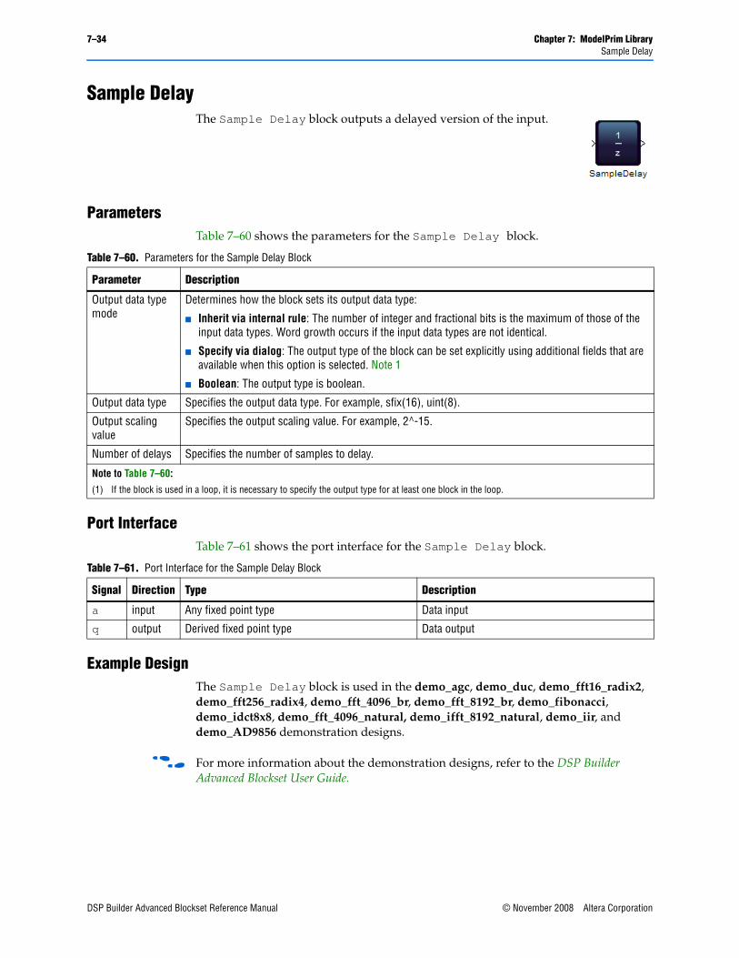
7–34 Chapter 7: ModelPrim LibrarySample Delay
Sample DelayThe Sample Delay block outputs a delayed version of the input.
ParametersTable 7–60 shows the parameters for the Sample Delay block.
Port InterfaceTable 7–61 shows the port interface for the Sample Delay block.
Example DesignThe Sample Delay block is used in the demo_agc, demo_duc, demo_fft16_radix2, demo_fft256_radix4, demo_fft_4096_br, demo_fft_8192_br, demo_fibonacci, demo_idct8x8, demo_fft_4096_natural, demo_ifft_8192_natural, demo_iir, and demo_AD9856 demonstration designs.
f For more information about the demonstration designs, refer to the DSP Builder Advanced Blockset User Guide.
Table 7–60. Parameters for the Sample Delay Block
Parameter Description
Output data type mode
Determines how the block sets its output data type:
■ Inherit via internal rule: The number of integer and fractional bits is the maximum of those of the input data types. Word growth occurs if the input data types are not identical.
■ Specify via dialog: The output type of the block can be set explicitly using additional fields that are available when this option is selected. Note 1
■ Boolean: The output type is boolean.
Output data type Specifies the output data type. For example, sfix(16), uint(8).
Output scaling value
Specifies the output scaling value. For example, 2^-15.
Number of delays Specifies the number of samples to delay.
Note to Table 7–60:
(1) If the block is used in a loop, it is necessary to specify the output type for at least one block in the loop.
Table 7–61. Port Interface for the Sample Delay Block
Signal Direction Type Description
a input Any fixed point type Data input
q output Derived fixed point type Data output
DSP Builder Advanced Blockset Reference Manual © November 2008 Altera Corporation
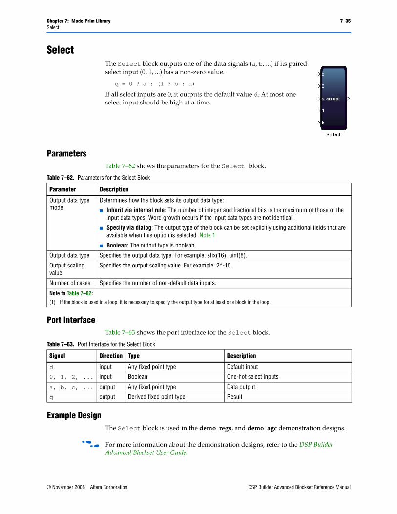
Chapter 7: ModelPrim Library 7–35Select
SelectThe Select block outputs one of the data signals (a, b, ...) if its paired select input (0, 1, ...) has a non-zero value.
q = 0 ? a : (1 ? b : d)
If all select inputs are 0, it outputs the default value d. At most one select input should be high at a time.
ParametersTable 7–62 shows the parameters for the Select block.
Port InterfaceTable 7–63 shows the port interface for the Select block.
Example DesignThe Select block is used in the demo_regs, and demo_agc demonstration designs.
f For more information about the demonstration designs, refer to the DSP Builder Advanced Blockset User Guide.
Table 7–62. Parameters for the Select Block
Parameter Description
Output data type mode
Determines how the block sets its output data type:
■ Inherit via internal rule: The number of integer and fractional bits is the maximum of those of the input data types. Word growth occurs if the input data types are not identical.
■ Specify via dialog: The output type of the block can be set explicitly using additional fields that are available when this option is selected. Note 1
■ Boolean: The output type is boolean.
Output data type Specifies the output data type. For example, sfix(16), uint(8).
Output scaling value
Specifies the output scaling value. For example, 2^-15.
Number of cases Specifies the number of non-default data inputs.
Note to Table 7–62:
(1) If the block is used in a loop, it is necessary to specify the output type for at least one block in the loop.
Table 7–63. Port Interface for the Select Block
Signal Direction Type Description
d input Any fixed point type Default input
0, 1, 2, ... input Boolean One-hot select inputs
a, b, c, ... output Any fixed point type Data output
q output Derived fixed point type Result
© November 2008 Altera Corporation DSP Builder Advanced Blockset Reference Manual
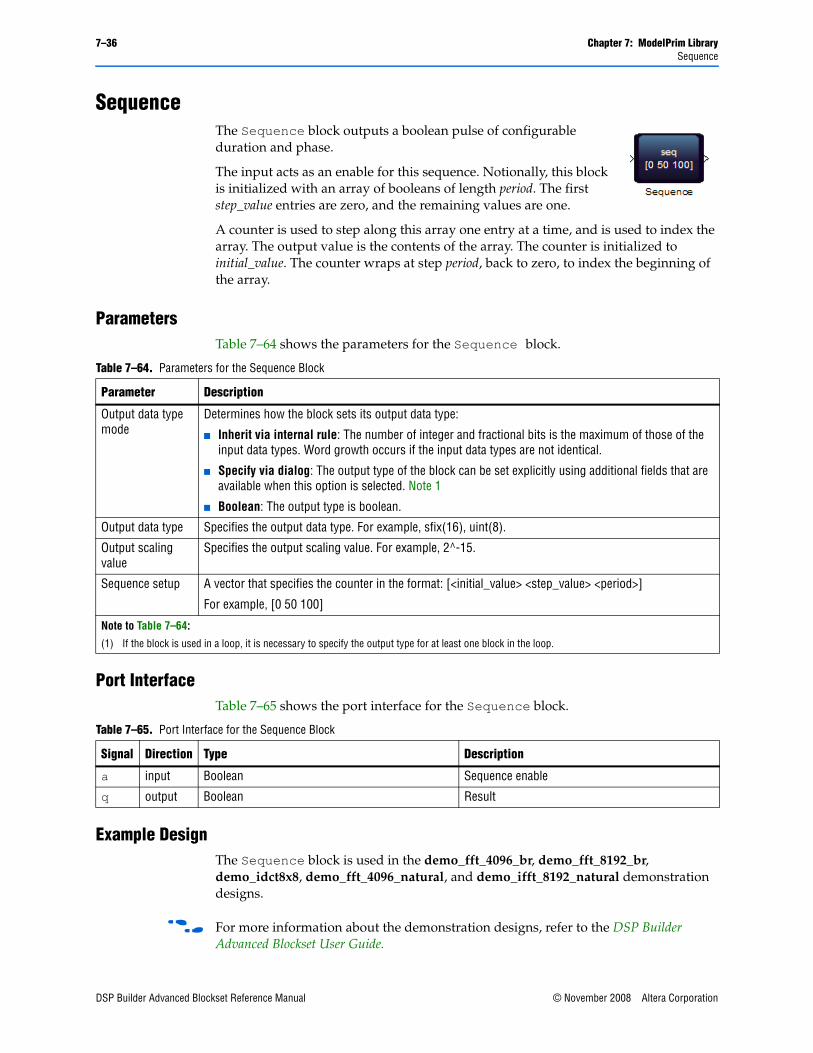
7–36 Chapter 7: ModelPrim LibrarySequence
SequenceThe Sequence block outputs a boolean pulse of configurable duration and phase.
The input acts as an enable for this sequence. Notionally, this block is initialized with an array of booleans of length period. The first step_value entries are zero, and the remaining values are one.
A counter is used to step along this array one entry at a time, and is used to index the array. The output value is the contents of the array. The counter is initialized to initial_value. The counter wraps at step period, back to zero, to index the beginning of the array.
ParametersTable 7–64 shows the parameters for the Sequence block.
Port InterfaceTable 7–65 shows the port interface for the Sequence block.
Example DesignThe Sequence block is used in the demo_fft_4096_br, demo_fft_8192_br, demo_idct8x8, demo_fft_4096_natural, and demo_ifft_8192_natural demonstration designs.
f For more information about the demonstration designs, refer to the DSP Builder Advanced Blockset User Guide.
Table 7–64. Parameters for the Sequence Block
Parameter Description
Output data type mode
Determines how the block sets its output data type:
■ Inherit via internal rule: The number of integer and fractional bits is the maximum of those of the input data types. Word growth occurs if the input data types are not identical.
■ Specify via dialog: The output type of the block can be set explicitly using additional fields that are available when this option is selected. Note 1
■ Boolean: The output type is boolean.
Output data type Specifies the output data type. For example, sfix(16), uint(8).
Output scaling value
Specifies the output scaling value. For example, 2^-15.
Sequence setup A vector that specifies the counter in the format: [<initial_value> <step_value> <period>]
For example, [0 50 100]
Note to Table 7–64:
(1) If the block is used in a loop, it is necessary to specify the output type for at least one block in the loop.
Table 7–65. Port Interface for the Sequence Block
Signal Direction Type Description
a input Boolean Sequence enable
q output Boolean Result
DSP Builder Advanced Blockset Reference Manual © November 2008 Altera Corporation
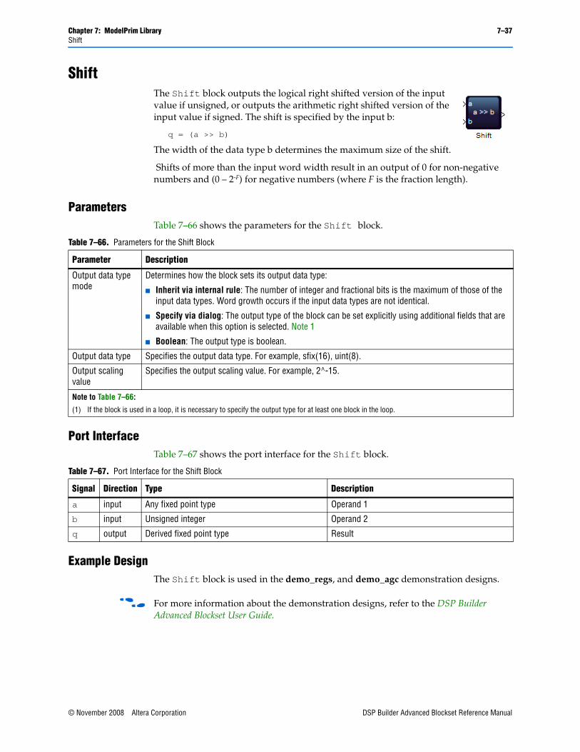
Chapter 7: ModelPrim Library 7–37Shift
ShiftThe Shift block outputs the logical right shifted version of the input value if unsigned, or outputs the arithmetic right shifted version of the input value if signed. The shift is specified by the input b:
q = (a >> b)
The width of the data type b determines the maximum size of the shift.
Shifts of more than the input word width result in an output of 0 for non-negative numbers and (0 – 2-F) for negative numbers (where F is the fraction length).
ParametersTable 7–66 shows the parameters for the Shift block.
Port InterfaceTable 7–67 shows the port interface for the Shift block.
Example DesignThe Shift block is used in the demo_regs, and demo_agc demonstration designs.
f For more information about the demonstration designs, refer to the DSP Builder Advanced Blockset User Guide.
Table 7–66. Parameters for the Shift Block
Parameter Description
Output data type mode
Determines how the block sets its output data type:
■ Inherit via internal rule: The number of integer and fractional bits is the maximum of those of the input data types. Word growth occurs if the input data types are not identical.
■ Specify via dialog: The output type of the block can be set explicitly using additional fields that are available when this option is selected. Note 1
■ Boolean: The output type is boolean.
Output data type Specifies the output data type. For example, sfix(16), uint(8).
Output scaling value
Specifies the output scaling value. For example, 2^-15.
Note to Table 7–66:
(1) If the block is used in a loop, it is necessary to specify the output type for at least one block in the loop.
Table 7–67. Port Interface for the Shift Block
Signal Direction Type Description
a input Any fixed point type Operand 1
b input Unsigned integer Operand 2
q output Derived fixed point type Result
© November 2008 Altera Corporation DSP Builder Advanced Blockset Reference Manual
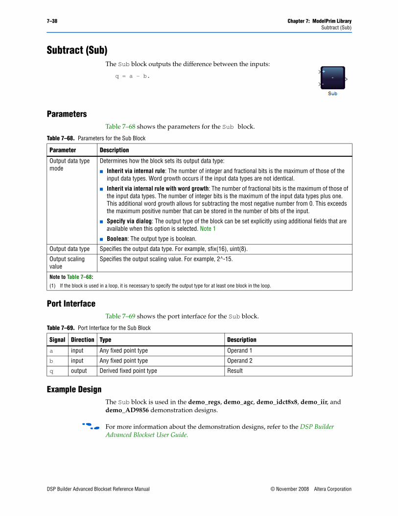
7–38 Chapter 7: ModelPrim LibrarySubtract (Sub)
Subtract (Sub)The Sub block outputs the difference between the inputs:
q = a – b.
ParametersTable 7–68 shows the parameters for the Sub block.
Port InterfaceTable 7–69 shows the port interface for the Sub block.
Example DesignThe Sub block is used in the demo_regs, demo_agc, demo_idct8x8, demo_iir, and demo_AD9856 demonstration designs.
f For more information about the demonstration designs, refer to the DSP Builder Advanced Blockset User Guide.
Table 7–68. Parameters for the Sub Block
Parameter Description
Output data type mode
Determines how the block sets its output data type:
■ Inherit via internal rule: The number of integer and fractional bits is the maximum of those of the input data types. Word growth occurs if the input data types are not identical.
■ Inherit via internal rule with word growth: The number of fractional bits is the maximum of those of the input data types. The number of integer bits is the maximum of the input data types plus one. This additional word growth allows for subtracting the most negative number from 0. This exceeds the maximum positive number that can be stored in the number of bits of the input.
■ Specify via dialog: The output type of the block can be set explicitly using additional fields that are available when this option is selected. Note 1
■ Boolean: The output type is boolean.
Output data type Specifies the output data type. For example, sfix(16), uint(8).
Output scaling value
Specifies the output scaling value. For example, 2^-15.
Note to Table 7–68:
(1) If the block is used in a loop, it is necessary to specify the output type for at least one block in the loop.
Table 7–69. Port Interface for the Sub Block
Signal Direction Type Description
a input Any fixed point type Operand 1
b input Any fixed point type Operand 2
q output Derived fixed point type Result
DSP Builder Advanced Blockset Reference Manual © November 2008 Altera Corporation
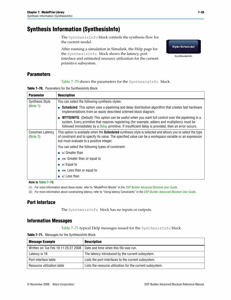
Chapter 7: ModelPrim Library 7–39Synthesis Information (SynthesisInfo)
Synthesis Information (SynthesisInfo)The SynthesisInfo block controls the synthesis flow for the current model.
After running a simulation in Simulink, the Help page for the SynthesisInfo block shows the latency, port interface and estimated resource utilization for the current primitive subsystem.
ParametersTable 7–70 shows the parameters for the SynthesisInfo block.
Port InterfaceThe SynthesisInfo block has no inputs or outputs.
Information MessagesTable 7–71 typical Help messages issued for the SynthesisInfo block.
Table 7–70. Parameters for the SynthesisInfo Block
Parameter Description
Synthesis Style (Note 1)
You can select the following synthesis styles:
■ Scheduled: This option uses a pipelining and delay distribution algorithm that creates fast hardware implementations from an easily described untimed block diagram.
■ WYYSIWYG: (Default) This option can be useful when you want full control over the pipelining in a system. Every primitive that requires registering (for example, adders and multipliers) must be followed immediately by a Delay primitive. If insufficient delay is provided, then an error occurs.
Constrain Latency (Note 2)
This option is available when the Scheduled synthesis style is selected and allows you to select the type of constraint and to specify its value. The specified value can be a workspace variable or an expression but must evaluate to a positive integer.
You can select the following types of constraint:
■ >: Greater than
■ >=: Greater than or equal to
■ =: Equal to
■ <=: Less than or equal to
■ <: Less than
Note to Table 7–70:
(1) For more information about these styles, refer to “ModelPrim Blocks” in the DSP Builder Advanced Blockset User Guide.(2) For more information about constraining latency, refer to “Using latency Constraints” in the DSP Builder Advanced Blockset User Guide.
Table 7–71. Messages for the SynthesisInfo Block
Message Example Description
Written on Tue Feb 19 11:25:27 2008 Date and time when this file was run.
Latency is 16 The latency introduced by the current subsystem.
Port interface table Lists the port interfaces to the current subsystem.
Resource utilization table Lists the resource utilization for the current subsystem.
© November 2008 Altera Corporation DSP Builder Advanced Blockset Reference Manual
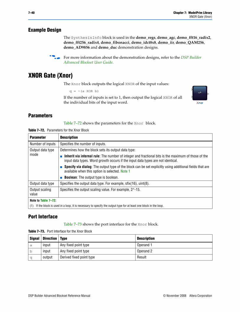
7–40 Chapter 7: ModelPrim LibraryXNOR Gate (Xnor)
Example DesignThe SynthesisInfo block is used in the demo_regs, demo_agc, demo_fft16_radix2, demo_fft256_radix4, demo_fibonacci, demo_idct8x8, demo_iir, demo_QAM256, demo_AD9856 and demo_duc demonstration designs.
f For more information about the demonstration designs, refer to the DSP Builder Advanced Blockset User Guide.
XNOR Gate (Xnor)The Xnor block outputs the logical XNOR of the input values:
q = ~(a XOR b)
If the number of inputs is set to 1, then output the logical XNOR of all the individual bits of the input word.
ParametersTable 7–72 shows the parameters for the Xnor block.
Port InterfaceTable 7–73 shows the port interface for the Xnor block.
Table 7–72. Parameters for the Xnor Block
Parameter Description
Number of inputs Specifies the number of inputs.
Output data type mode
Determines how the block sets its output data type:
■ Inherit via internal rule: The number of integer and fractional bits is the maximum of those of the input data types. Word growth occurs if the input data types are not identical.
■ Specify via dialog: The output type of the block can be set explicitly using additional fields that are available when this option is selected. Note 1
■ Boolean: The output type is boolean.
Output data type Specifies the output data type. For example, sfix(16), uint(8).
Output scaling value
Specifies the output scaling value. For example, 2^-15.
Note to Table 7–72:
(1) If the block is used in a loop, it is necessary to specify the output type for at least one block in the loop.
Table 7–73. Port Interface for the Xnor Block
Signal Direction Type Description
a input Any fixed point type Operand 1
b input Any fixed point type Operand 2
q output Derived fixed point type Result
DSP Builder Advanced Blockset Reference Manual © November 2008 Altera Corporation
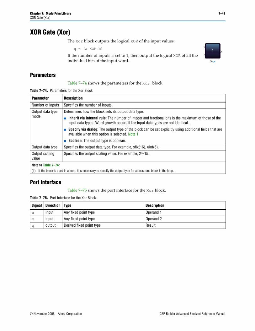
Chapter 7: ModelPrim Library 7–41XOR Gate (Xor)
XOR Gate (Xor)The Xor block outputs the logical XOR of the input values:
q = (a XOR b)
If the number of inputs is set to 1, then output the logical XOR of all the individual bits of the input word.
ParametersTable 7–74 shows the parameters for the Xor block.
Port InterfaceTable 7–75 shows the port interface for the Xor block.
Table 7–74. Parameters for the Xor Block
Parameter Description
Number of inputs Specifies the number of inputs.
Output data type mode
Determines how the block sets its output data type:
■ Inherit via internal rule: The number of integer and fractional bits is the maximum of those of the input data types. Word growth occurs if the input data types are not identical.
■ Specify via dialog: The output type of the block can be set explicitly using additional fields that are available when this option is selected. Note 1
■ Boolean: The output type is boolean.
Output data type Specifies the output data type. For example, sfix(16), uint(8).
Output scaling value
Specifies the output scaling value. For example, 2^-15.
Note to Table 7–74:
(1) If the block is used in a loop, it is necessary to specify the output type for at least one block in the loop.
Table 7–75. Port Interface for the Xor Block
Signal Direction Type Description
a input Any fixed point type Operand 1
b input Any fixed point type Operand 2
q output Derived fixed point type Result
© November 2008 Altera Corporation DSP Builder Advanced Blockset Reference Manual

7–42 Chapter 7: ModelPrim LibraryXOR Gate (Xor)
DSP Builder Advanced Blockset Reference Manual © November 2008 Altera Corporation
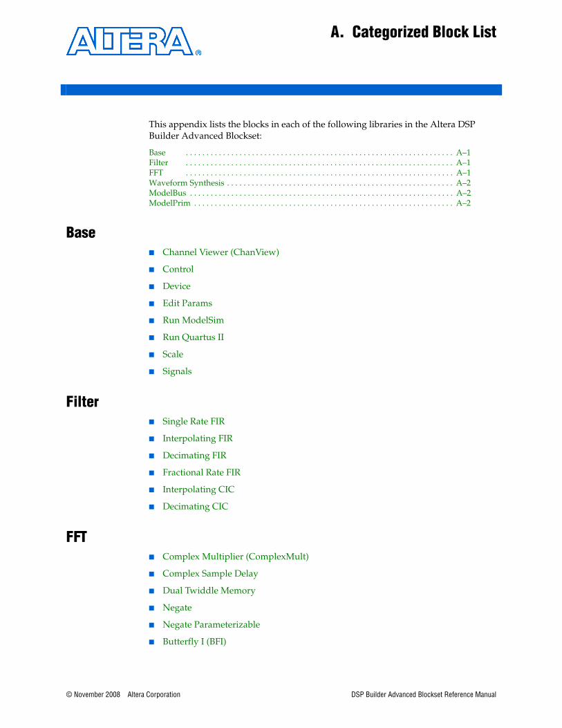
© November 2008 Altera Corporation
A. Categorized Block List
This appendix lists the blocks in each of the following libraries in the Altera DSP Builder Advanced Blockset:
Base . . . . . . . . . . . . . . . . . . . . . . . . . . . . . . . . . . . . . . . . . . . . . . . . . . . . . . . . . . . . . . . . . A–1Filter . . . . . . . . . . . . . . . . . . . . . . . . . . . . . . . . . . . . . . . . . . . . . . . . . . . . . . . . . . . . . . . . . A–1FFT . . . . . . . . . . . . . . . . . . . . . . . . . . . . . . . . . . . . . . . . . . . . . . . . . . . . . . . . . . . . . . . . . A–1Waveform Synthesis . . . . . . . . . . . . . . . . . . . . . . . . . . . . . . . . . . . . . . . . . . . . . . . . . . . . . . . A–2ModelBus . . . . . . . . . . . . . . . . . . . . . . . . . . . . . . . . . . . . . . . . . . . . . . . . . . . . . . . . . . . . . . . . A–2ModelPrim . . . . . . . . . . . . . . . . . . . . . . . . . . . . . . . . . . . . . . . . . . . . . . . . . . . . . . . . . . . . . . . A–2
Base■ Channel Viewer (ChanView)
■ Control
■ Device
■ Edit Params
■ Run ModelSim
■ Run Quartus II
■ Scale
■ Signals
Filter ■ Single Rate FIR
■ Interpolating FIR
■ Decimating FIR
■ Fractional Rate FIR
■ Interpolating CIC
■ Decimating CIC
FFT■ Complex Multiplier (ComplexMult)
■ Complex Sample Delay
■ Dual Twiddle Memory
■ Negate
■ Negate Parameterizable
■ Butterfly I (BFI)
DSP Builder Advanced Blockset Reference Manual
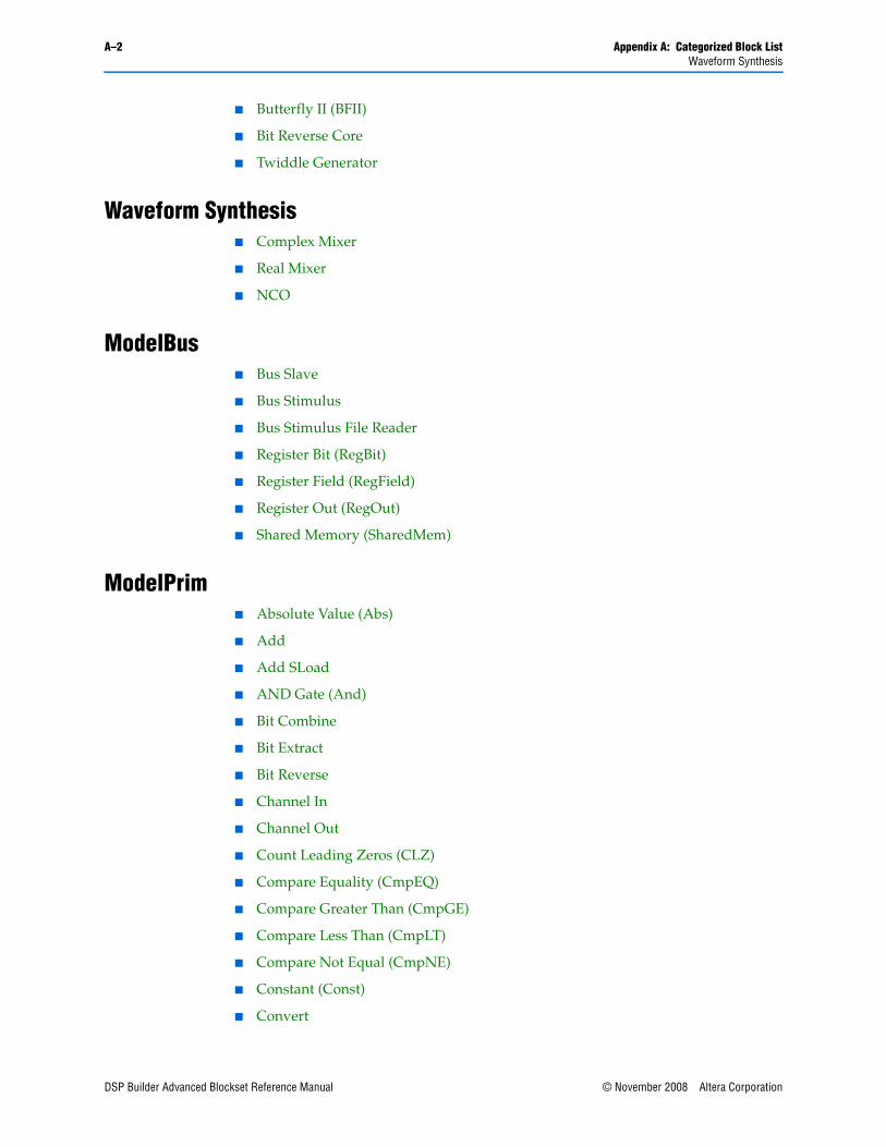
A–2 Appendix A: Categorized Block ListWaveform Synthesis
■ Butterfly II (BFII)
■ Bit Reverse Core
■ Twiddle Generator
Waveform Synthesis■ Complex Mixer
■ Real Mixer
■ NCO
ModelBus■ Bus Slave
■ Bus Stimulus
■ Bus Stimulus File Reader
■ Register Bit (RegBit)
■ Register Field (RegField)
■ Register Out (RegOut)
■ Shared Memory (SharedMem)
ModelPrim■ Absolute Value (Abs)
■ Add
■ Add SLoad
■ AND Gate (And)
■ Bit Combine
■ Bit Extract
■ Bit Reverse
■ Channel In
■ Channel Out
■ Count Leading Zeros (CLZ)
■ Compare Equality (CmpEQ)
■ Compare Greater Than (CmpGE)
■ Compare Less Than (CmpLT)
■ Compare Not Equal (CmpNE)
■ Constant (Const)
■ Convert
DSP Builder Advanced Blockset Reference Manual © November 2008 Altera Corporation
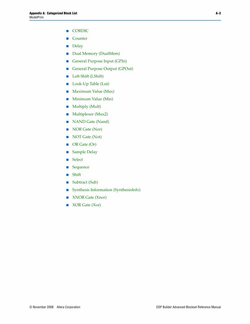
Appendix A: Categorized Block List A–3ModelPrim
■ CORDIC
■ Counter
■ Delay
■ Dual Memory (DualMem)
■ General Purpose Input (GPIn)
■ General Purpose Output (GPOut)
■ Left Shift (LShift)
■ Look-Up Table (Lut)
■ Maximum Value (Max)
■ Minimum Value (Min)
■ Multiply (Mult)
■ Multiplexer (Mux2)
■ NAND Gate (Nand)
■ NOR Gate (Nor)
■ NOT Gate (Not)
■ OR Gate (Or)
■ Sample Delay
■ Select
■ Sequence
■ Shift
■ Subtract (Sub)
■ Synthesis Information (SynthesisInfo)
■ XNOR Gate (Xnor)
■ XOR Gate (Xor)
© November 2008 Altera Corporation DSP Builder Advanced Blockset Reference Manual

A–4 Appendix A: Categorized Block ListModelPrim
DSP Builder Advanced Blockset Reference Manual © November 2008 Altera Corporation
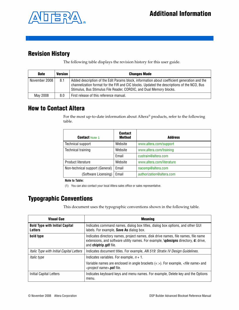
© November 2008 Altera Corporation
Additional Information
Revision History The following table displays the revision history for this user guide.
How to Contact AlteraFor the most up-to-date information about Altera® products, refer to the following table.
Typographic ConventionsThis document uses the typographic conventions shown in the following table.
Date Version Changes Made
November 2008 8.1 Added description of the Edit Params block, information about coefficient generation and the channelization format for the FIR and CIC blocks. Updated the descriptions of the NCO, Bus Stimulus, Bus Stimulus File Reader, CORDIC, and Dual Memory blocks.
May 2008 8.0 First release of this reference manual.
Contact Note 1Contact Method Address
Technical support Website www.altera.com/support
Technical training Website www.altera.com/training
Email [email protected]
Product literature Website www.altera.com/literature
Non-technical support (General) Email [email protected]
(Software Licensing) Email [email protected]
Note to Table:
(1) You can also contact your local Altera sales office or sales representative.
Visual Cue Meaning
Bold Type with Initial Capital Letters
Indicates command names, dialog box titles, dialog box options, and other GUI labels. For example, Save As dialog box.
bold type Indicates directory names, project names, disk drive names, file names, file name extensions, and software utility names. For example, \qdesigns directory, d: drive, and chiptrip.gdf file.
Italic Type with Initial Capital Letters Indicates document titles. For example, AN 519: Stratix IV Design Guidelines.
Italic type Indicates variables. For example, n + 1.
Variable names are enclosed in angle brackets (< >). For example, <file name> and <project name>.pof file.
Initial Capital Letters Indicates keyboard keys and menu names. For example, Delete key and the Options menu.
DSP Builder Advanced Blockset Reference Manual
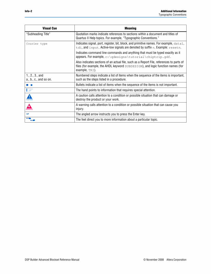
Info–2 Additional InformationTypographic Conventions
“Subheading Title” Quotation marks indicate references to sections within a document and titles of Quartus II Help topics. For example, “Typographic Conventions.”
Courier type Indicates signal, port, register, bit, block, and primitive names. For example, data1, tdi, and input. Active-low signals are denoted by suffix n. Example: resetn.
Indicates command line commands and anything that must be typed exactly as it appears. For example, c:\qdesigns\tutorial\chiptrip.gdf.
Also indicates sections of an actual file, such as a Report File, references to parts of files (for example, the AHDL keyword SUBDESIGN), and logic function names (for example, TRI).
1., 2., 3., anda., b., c., and so on.
Numbered steps indicate a list of items when the sequence of the items is important, such as the steps listed in a procedure.
■ ■ Bullets indicate a list of items when the sequence of the items is not important.
1 The hand points to information that requires special attention.
c A caution calls attention to a condition or possible situation that can damage or destroy the product or your work.
w A warning calls attention to a condition or possible situation that can cause you injury.
r The angled arrow instructs you to press the Enter key.
f The feet direct you to more information about a particular topic.
Visual Cue Meaning
DSP Builder Advanced Blockset Reference Manual © November 2008 Altera Corporation
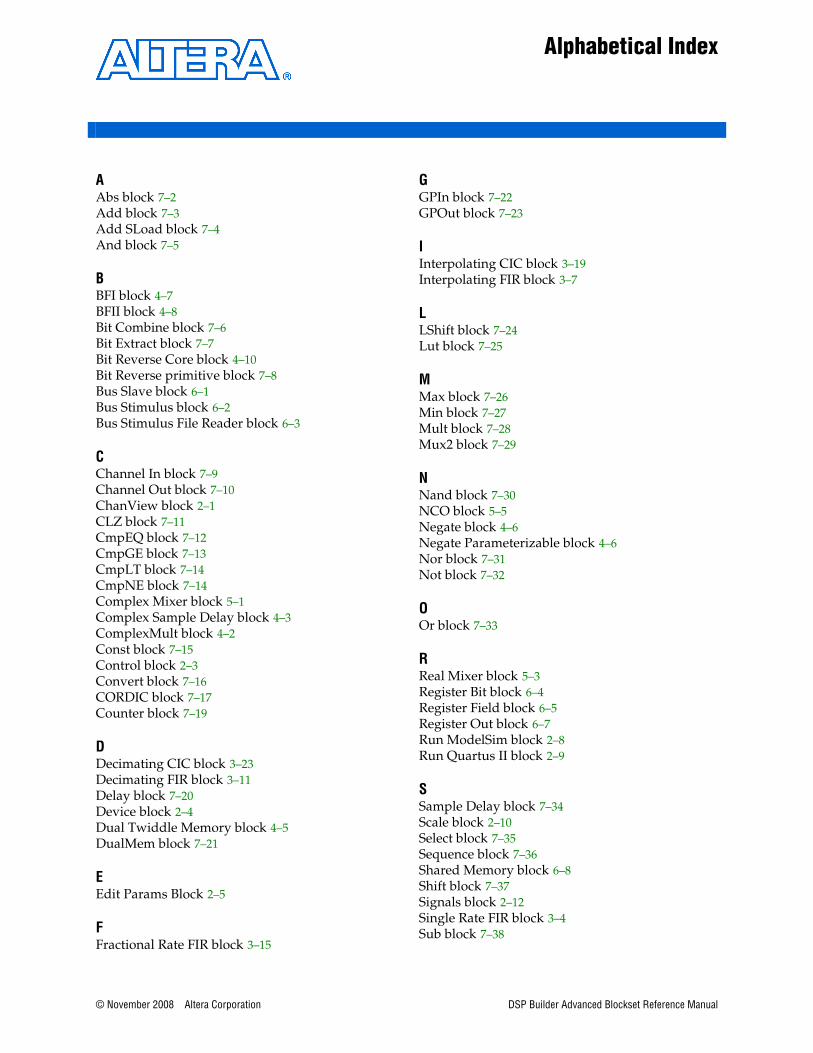
© November 2008 Altera Corporation
Alphabetical Index
AAbs block 7–2Add block 7–3Add SLoad block 7–4And block 7–5
BBFI block 4–7BFII block 4–8Bit Combine block 7–6Bit Extract block 7–7Bit Reverse Core block 4–10Bit Reverse primitive block 7–8Bus Slave block 6–1Bus Stimulus block 6–2Bus Stimulus File Reader block 6–3
CChannel In block 7–9Channel Out block 7–10ChanView block 2–1CLZ block 7–11CmpEQ block 7–12CmpGE block 7–13CmpLT block 7–14CmpNE block 7–14Complex Mixer block 5–1Complex Sample Delay block 4–3ComplexMult block 4–2Const block 7–15Control block 2–3Convert block 7–16CORDIC block 7–17Counter block 7–19
DDecimating CIC block 3–23Decimating FIR block 3–11Delay block 7–20Device block 2–4Dual Twiddle Memory block 4–5DualMem block 7–21
EEdit Params Block 2–5
FFractional Rate FIR block 3–15
GGPIn block 7–22GPOut block 7–23
IInterpolating CIC block 3–19Interpolating FIR block 3–7
LLShift block 7–24Lut block 7–25
MMax block 7–26Min block 7–27Mult block 7–28Mux2 block 7–29
NNand block 7–30NCO block 5–5Negate block 4–6Negate Parameterizable block 4–6Nor block 7–31Not block 7–32
OOr block 7–33
RReal Mixer block 5–3Register Bit block 6–4Register Field block 6–5Register Out block 6–7Run ModelSim block 2–8Run Quartus II block 2–9
SSample Delay block 7–34Scale block 2–10Select block 7–35Sequence block 7–36Shared Memory block 6–8Shift block 7–37Signals block 2–12Single Rate FIR block 3–4Sub block 7–38
DSP Builder Advanced Blockset Reference Manual

Index–2
SynthesisInfo block 7–39
TTwiddle Generator block 4–11
XXnor block 7–40Xor block 7–41
DSP Builder Advanced Blockset Reference Manual © November 2008 Altera Corporation