dsk c6713b - ipfwlin/ecet357/ti-tms320c6713dsk/dsk6713_techref.pdf3-11 3.8 reset switch ... starter...
TRANSCRIPT

TMS320C6713 DSK
2003 DSP Development Systems
ReferenceTechnical

TMS320C6713 DSK Technical Reference
506735-0001 Rev. B November 2003
SPECTRUM DIGITAL, INC.12502 Exchange Drive, Suite 440 Stafford, TX. 77477
Tel: 281.494.4505 Fax: [email protected] www.spectrumdigital.com

IMPORTANT NOTICE
Spectrum Digital, Inc. reserves the right to make changes to its products or to discontinue anyproduct or service without notice. Customers are advised to obtain the latest version of relevantinformation to verify that the data being relied on is current before placing orders.
Spectrum Digital, Inc. warrants performance of its products and related software to currentspecifications in accordance with Spectrum Digital’s standard warranty. Testing and other qualitycontrol techniques are utilized to the extent deemed necessary to support this warranty.
Please be aware that the products described herein are not intended for use in life-support appliances, devices, or systems. Spectrum Digital does not warrant nor is Spectrum Digital liable for the product described herein to be used in other than a development environment.
Spectrum Digital, Inc. assumes no liability for applications assistance, customer product design, software performance, or infringement of patents or services described herein. Nor does SpectrumDigital warrant or represent any license, either express or implied, is granted under any patent right,copyright, or other intellectual property right of Spectrum Digital, Inc. covering or relating to anycombination, machine, or process in which such Digital Signal Processing development products orservices might be or are used.
WARNING
This equipment is intended for use in a laboratory test environment only. It generates, uses, and canradiate radio frequency energy and has not been tested for compliance with the limits of computingdevices pursuant to subpart J of part 15 of FCC rules, which are designed to provide reasonableprotection against radio frequency interference. Operation of this equipment in other environmentsmay cause interference with radio communications, in which case the user at his own expense will berequired to take whatever measures necessary to correct this interference.
Copyright © 2003 Spectrum Digital, Inc.
Contents
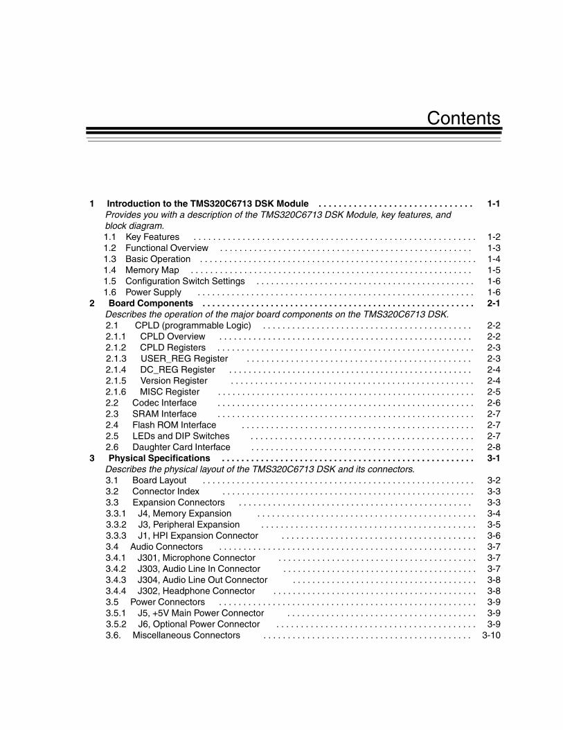
1 Introduction to the TMS320C6713 DSK Module . . . . . . . . . . . . . . . . . . . . . . . . . . . . . . . 1-1 Provides you with a description of the TMS320C6713 DSK Module, key features, and block diagram. 1.1 Key Features . . . . . . . . . . . . . . . . . . . . . . . . . . . . . . . . . . . . . . . . . . . . . . . . . . . . . . . . . . 1-2 1.2 Functional Overview . . . . . . . . . . . . . . . . . . . . . . . . . . . . . . . . . . . . . . . . . . . . . . . . . . . . 1-3 1.3 Basic Operation . . . . . . . . . . . . . . . . . . . . . . . . . . . . . . . . . . . . . . . . . . . . . . . . . . . . . . . . . 1-4 1.4 Memory Map . . . . . . . . . . . . . . . . . . . . . . . . . . . . . . . . . . . . . . . . . . . . . . . . . . . . . . . . . . 1-5 1.5 Configuration Switch Settings . . . . . . . . . . . . . . . . . . . . . . . . . . . . . . . . . . . . . . . . . . . . . 1-6 1.6 Power Supply . . . . . . . . . . . . . . . . . . . . . . . . . . . . . . . . . . . . . . . . . . . . . . . . . . . . . . . . . 1-62 Board Components . . . . . . . . . . . . . . . . . . . . . . . . . . . . . . . . . . . . . . . . . . . . . . . . . . . . . . . . 2-1 Describes the operation of the major board components on the TMS320C6713 DSK. 2.1 CPLD (programmable Logic) . . . . . . . . . . . . . . . . . . . . . . . . . . . . . . . . . . . . . . . . . . . 2-2 2.1.1 CPLD Overview . . . . . . . . . . . . . . . . . . . . . . . . . . . . . . . . . . . . . . . . . . . . . . . . . . . . 2-2 2.1.2 CPLD Registers . . . . . . . . . . . . . . . . . . . . . . . . . . . . . . . . . . . . . . . . . . . . . . . . . . . . . 2-3 2.1.3 USER_REG Register . . . . . . . . . . . . . . . . . . . . . . . . . . . . . . . . . . . . . . . . . . . . . . 2-3 2.1.4 DC_REG Register . . . . . . . . . . . . . . . . . . . . . . . . . . . . . . . . . . . . . . . . . . . . . . . . . . 2-4 2.1.5 Version Register . . . . . . . . . . . . . . . . . . . . . . . . . . . . . . . . . . . . . . . . . . . . . . . . . . 2-4 2.1.6 MISC Register . . . . . . . . . . . . . . . . . . . . . . . . . . . . . . . . . . . . . . . . . . . . . . . . . . . . . 2-5 2.2 Codec Interface . . . . . . . . . . . . . . . . . . . . . . . . . . . . . . . . . . . . . . . . . . . . . . . . . . . . . 2-6 2.3 SRAM Interface . . . . . . . . . . . . . . . . . . . . . . . . . . . . . . . . . . . . . . . . . . . . . . . . . . . . . 2-7 2.4 Flash ROM Interface . . . . . . . . . . . . . . . . . . . . . . . . . . . . . . . . . . . . . . . . . . . . . . . . 2-7 2.5 LEDs and DIP Switches . . . . . . . . . . . . . . . . . . . . . . . . . . . . . . . . . . . . . . . . . . . . . . 2-7 2.6 Daughter Card Interface . . . . . . . . . . . . . . . . . . . . . . . . . . . . . . . . . . . . . . . . . . . . . . 2-83 Physical Specifications . . . . . . . . . . . . . . . . . . . . . . . . . . . . . . . . . . . . . . . . . . . . . . . . . . . . 3-1 Describes the physical layout of the TMS320C6713 DSK and its connectors. 3.1 Board Layout . . . . . . . . . . . . . . . . . . . . . . . . . . . . . . . . . . . . . . . . . . . . . . . . . . . . . . . . 3-2 3.2 Connector Index . . . . . . . . . . . . . . . . . . . . . . . . . . . . . . . . . . . . . . . . . . . . . . . . . . . . 3-3 3.3 Expansion Connectors . . . . . . . . . . . . . . . . . . . . . . . . . . . . . . . . . . . . . . . . . . . . . . . . 3-3 3.3.1 J4, Memory Expansion . . . . . . . . . . . . . . . . . . . . . . . . . . . . . . . . . . . . . . . . . . . . . 3-4 3.3.2 J3, Peripheral Expansion . . . . . . . . . . . . . . . . . . . . . . . . . . . . . . . . . . . . . . . . . . . . 3-5 3.3.3 J1, HPI Expansion Connector . . . . . . . . . . . . . . . . . . . . . . . . . . . . . . . . . . . . . . . . 3-6 3.4 Audio Connectors . . . . . . . . . . . . . . . . . . . . . . . . . . . . . . . . . . . . . . . . . . . . . . . . . . . . . 3-7 3.4.1 J301, Microphone Connector . . . . . . . . . . . . . . . . . . . . . . . . . . . . . . . . . . . . . . . . . 3-7 3.4.2 J303, Audio Line In Connector . . . . . . . . . . . . . . . . . . . . . . . . . . . . . . . . . . . . . . . . 3-7 3.4.3 J304, Audio Line Out Connector . . . . . . . . . . . . . . . . . . . . . . . . . . . . . . . . . . . . . . 3-8 3.4.4 J302, Headphone Connector . . . . . . . . . . . . . . . . . . . . . . . . . . . . . . . . . . . . . . . . . . 3-8 3.5 Power Connectors . . . . . . . . . . . . . . . . . . . . . . . . . . . . . . . . . . . . . . . . . . . . . . . . . . . . . 3-9 3.5.1 J5, +5V Main Power Connector . . . . . . . . . . . . . . . . . . . . . . . . . . . . . . . . . . . . . . . 3-9 3.5.2 J6, Optional Power Connector . . . . . . . . . . . . . . . . . . . . . . . . . . . . . . . . . . . . . . . . . 3-9 3.6. Miscellaneous Connectors . . . . . . . . . . . . . . . . . . . . . . . . . . . . . . . . . . . . . . . . . . . 3-10

3.6.1 J201, USB Port . . . . . . . . . . . . . . . . . . . . . . . . . . . . . . . . . . . . . . . . . . . . . . . . . . . . 3-10 3.6.2 J8, External JTAG Connector . . . . . . . . . . . . . . . . . . . . . . . . . . . . . . . . . . . . . . . . 3-10 3.6.3 JP3, PLD Programming Connector . . . . . . . . . . . . . . . . . . . . . . . . . . . . . . . . . . . . . 3-11 3.7 System LEDs . . . . . . . . . . . . . . . . . . . . . . . . . . . . . . . . . . . . . . . . . . . . . . . . . . . . . . . 3-11 3.8 Reset Switch . . . . . . . . . . . . . . . . . . . . . . . . . . . . . . . . . . . . . . . . . . . . . . . . . . . . . . . 3-11A Schematics . . . . . . . . . . . . . . . . . . . . . . . . . . . . . . . . . . . . . . . . . . . . . . . . . . . . . . . . . . . . . . A-1 Contains the schematics for the TMS320C6713 DSKB Mechanical Information . . . . . . . . . . . . . . . . . . . . . . . . . . . . . . . . . . . . . . . . . . . . . . . . . . B-1 Contains the mechanical information about the TMS320C6713 DSK

About This Manual
This document describes the board level operations of the TMS320C6713 DSPStarter Kit (DSK) module. The DSK is based on the Texas Instruments TMS320C6713 Digital Signal Processor.
The TMS320C6713 DSK is a table top card to allow engineers and softwaredevelopers to evaluate certain characteristics of the TMS320C6713 DSP to determineif the processor meets the designers application requirements. Evaluators can createsoftware to execute onboard or expand the system in a variety of ways.
Notational Conventions
This document uses the following conventions.
The TMS320C6713 DSK will sometimes be referred to as the DSK.
Program listings, program examples, and interactive displays are shown is a specialitalic typeface. Here is a sample program listing.
equations!rd = !strobe&rw;
Information About Cautions
This book may contain cautions.This is an example of a caution statement.A caution statement describes a situation that could potentially damage your software,or hardware, or other equipment. The information in a caution is provided for yourprotection. Please read each caution carefully.
Related Documents
Texas Instruments TMS320C67xx DSP CPU Reference GuideTexas Instruments TMS320C67xx DSP Peripherals Reference Guide

Table 1: Manual History
Revision History
A Alpha Release

1-1
Chapter 1
Introduction to the TMS320C6713 DSK
Chapter One provides a description of the TMS320C6713 DSK alongwith the key features and a block diagram of the circuit board.
Topic Page
1.1 Key Features 1-21.2 Functional Overview 1-31.3 Basic Operation 1-41.4 Memory Map 1-51.5 Configuration Switch Settings 1-61.6 Power Supply 1-6

Spectrum Digital, Inc
1-2 TMS320C6713 DSK Module Technical Reference
1.1 Key Features
The C6713 DSK is a low-cost standalone development platform that enables users toevaluate and develop applications for the TI C67xx DSP family. The DSK also servesas a hardware reference design for the TMS320C6713 DSP. Schematics, logicequations and application notes are available to ease hardware development andreduce time to market.
The DSK comes with a full compliment of on-board devices that suit a wide variety ofapplication environments. Key features include:
• A Texas Instruments TMS320C6713 DSP operating at 225 MHz.
• An AIC23 stereo codec
• 16 Mbytes of synchronous DRAM
• 512 Kbytes of non-volatile Flash memory (256 Kbytes usable in default configuration)
• 4 user accessible LEDs and DIP switches
• Software board configuration through registers implemented in CPLD
• Configurable boot options
• Standard expansion connectors for daughter card use
• JTAG emulation through on-board JTAG emulator with USB host interface or external emulator
• Single voltage power supply (+5V)
Figure 1-1, Block Diagram C6713 DSK
Ext.JTAG
AIC23Codec
Hos
t Por
t Int
MUX
MUX
MIC
IN
LIN
E O
UT
HP
OU
T
LIN
E IN
Peripheral Exp
LED DIP
EMIF
HPI
McBSPs
JTAG
0 1 2 30 1 2 3
CPL
D
Memory Exp
PWR
USB
EmbeddedJTAG
JP1 1.26V
JP2 3.3V
END
IAN
BOO
TM 1
BOO
TM 0
6713DSP
SDR
AM
328
Flas
h
8
1 32
ConfigSW3
32
HPI
_EN
4
VoltageReg
JP4
5V

Spectrum Digital, Inc
1-3
1.2 Functional Overview of the TMS320C6713 DSK
The DSP on the 6713 DSK interfaces to on-board peripherals through a 32-bit wideEMIF (External Memory InterFace). The SDRAM, Flash and CPLD are all connectedto the bus. EMIF signals are also connected daughter card expansion connectorswhich are used for third party add-in boards.
The DSP interfaces to analog audio signals through an on-board AIC23 codec and four3.5 mm audio jacks (microphone input, line input, line output, and headphone output).The codec can select the microphone or the line input as the active input. The analogoutput is driven to both the line out (fixed gain) and headphone (adjustable gain)connectors. McBSP0 is used to send commands to the codec control interface whileMcBSP1 is used for digital audio data. McBSP0 and McBSP1 can be re-routed to theexpansion connectors in software.
A programmable logic device called a CPLD is used to implement glue logic that tiesthe board components together. The CPLD has a register based user interface thatlets the user configure the board by reading and writing to its registers.
The DSK includes 4 LEDs and a 4 position DIP switch as a simple way to provide theuser with interactive feedback. Both are accessed by reading and writing to the CPLDregisters.
An included 5V external power supply is used to power the board. On-board switchingvoltage regulators provide the +1.26V DSP core voltage and +3.3V I/O supplies. Theboard is held in reset until these supplies are within operating specifications.
Code Composer communicates with the DSK through an embedded JTAG emulatorwith a USB host interface. The DSK can also be used with an external emulatorthrough the external JTAG connector.
Spectrum Digital, Inc
1-4 TMS320C6713 DSK Module Technical Reference
1.3 Basic Operation
The DSK is designed to work with TI’s Code Composer Studio developmentenvironment and ships with a version specifically tailored to work with the board.Code Composer communicates with the board through the on-board JTAG emulator.To start, follow the instructions in the Quick Start Guide to install Code Composer. This process will install all of the necessary development tools, documentation anddrivers.
After the install is complete, follow these steps to run Code Composer. The DSK mustbe fully connected to launch the DSK version of Code Composer.
1) Connect the included power supply to the DSK.
2) Connect the DSK to your PC with a standard USB cable (also included).
3) Launch Code Composer from its icon on your desktop.
Detailed information about the DSK including a tutorial, examples and referencematerial is available in the DSK’s help file. You can access the help file through CodeComposer’s help menu. It can also be launched directly by double-clicking on the filec6713dsk.hlp in Code Composer’s docs\hlp subdirectory.

Spectrum Digital, Inc
1-5
1.4 Memory Map
The C67xx family of DSPs has a large byte addressable address space. Program codeand data can be placed anywhere in the unified address space. Addresses are always32-bits wide.
The memory map shows the address space of a generic 6713 processor on the leftwith specific details of how each region is used on the right. By default, the internalmemory sits at the beginning of the address space. Portions of the internal memorycan be reconfigured in software as L2 cache rather than fixed RAM.
The EMIF has 4 separate addressable regions called chip enable spaces (CE0-CE3). The SDRAM occupies CE0 while the Flash and CPLD share CE1. CE2 and CE3 aregenerally reserved for daughtercards.
Figure 1-2, Memory Map, C6713 DSK
Internal Memory
Reserved Spaceor
Peripheral Regs
AddressC67x Family
Memory Type
SDRAM
CPLDFlash
DaughterCard
6713 DSK
InternalMemory
Reservedor
Peripheral
EMIF CE0
EMIF CE3
EMIF CE2
EMIF CE1
0x80000000
0x90000000
0xA0000000
0xB0000000
0x00000000
0x00030000
0x90080000

Spectrum Digital, Inc
1-6 TMS320C6713 DSK Module Technical Reference
1.5 Configuration Switch Settings
The DSK has 4 configuration switches that allows users to control the operational stateof the DSP when it is released from reset. The configuration switch block is labeledSW3 on the DSK board, next to the reset switch.
Configuration switch 1 controls the endianness of the DSP while switches 2 and 3configure the boot mode that will be used when the DSP starts executing. Configuration switch 4 controls the on-chip multiplexing of HPI and McASP signalsbrought out to the HPI expansion connector. By default all switches are off whichcorresponds to EMIF boot (out of 8-bit Flash) in little endian mode and HPI signals onthe HPI expansion connector.
1.6 Power Supply
The DSK operates from a single +5V external power supply connected to the mainpower input (J5). Internally, the +5V input is converted into +1.26V and +3.3V usingseparate voltage regulators. The +1.26V supply is used for the DSP core while the+3.3V supply is used for the DSP's I/O buffers and all other chips on the board. Thepower connector is a 2.5mm barrel-type plug.
There are three power test points on the DSK at JP1, JP2 and JP4. All I/O currentpasses through JP2 while all core current passes through JP1. All system currentpasses through JP4. Normally these jumpers are closed. To measure the currentpassing through remove the jumpers and connect the pins with a current measuringdevice such as a multimeter or current probe.
It is possible to provide the daughter card with +12V and -12V when the external powerconnector (J6) is used.
Table 1: Configuration Switch Settings
Switch 1 Switch 2 Switch 3 Switch 4 Configuration Description
Off Little endian (default)
On Big endian
Off Off EMIF boot from 8-bit Flash (default)
Off On HPI/Emulation boot
On Off 32-bit EMIF boot
On On 16-bit EMIF boot
Off HPI enabled on HPI pins (default)
On McASP1 enabled on HPI pins
2-1
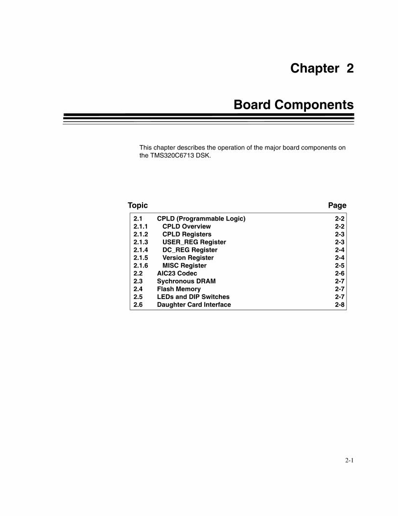
Chapter 2
Board Components
This chapter describes the operation of the major board components onthe TMS320C6713 DSK.
Topic Page
2.1 CPLD (Programmable Logic) 2-22.1.1 CPLD Overview 2-22.1.2 CPLD Registers 2-32.1.3 USER_REG Register 2-32.1.4 DC_REG Register 2-42.1.5 Version Register 2-42.1.6 MISC Register 2-52.2 AIC23 Codec 2-62.3 Sychronous DRAM 2-72.4 Flash Memory 2-72.5 LEDs and DIP Switches 2-72.6 Daughter Card Interface 2-8
Spectrum Digital, Inc
2-2 TMS320C6713 DSK Module Technical Reference
2.1 CPLD (Programmable Logic)
The C6713 DSK uses an Altera EPM3128TC100-10 Complex Programmable LogicDevice (CPLD) device to implement:
• 4 Memory-mapped control/status registers that allow software control of various board features.
• Control of the daughter card interface and signals.
• Assorted "glue" logic that ties the board components together.
2.1.1 CPLD Overview
The CPLD logic is used to implement functionality specific to the DSK. Your ownhardware designs will likely implement a completely different set of functions or takeadvantage of the DSPs high level of integration for system design and avoid the use of external logic completely.
The CPLD implements simple random logic functions that eliminate the need foradditional discrete devices. In particular, the CPLD aggregates the various resetsignals coming from the reset button and power supervisors and generates a globalreset.
The EPM3128TC100-10 is a 3.3V (5V tolerant), 100-pin QFP device that provides 128 macrocells, 80 I/O pins, and a 10 ns pin-to-pin delay. The device is EEPROM-based and is in-system programmable via a dedicated JTAG interface (a 10-pin header on the DSK). The CPLD source files are written in the industrystandard VHDL (Hardware Design Language) and included with the DSK.

Spectrum Digital, Inc
2-3
2.1.2 CPLD Registers
The 4 CPLD memory-mapped registers allows users to control CPLD functions insoftware. On the 6713 DSK the registers are primarily used to access the LEDs andDIP switches and control the daughter card interface. The registers are mapped intoEMIF CE1 data space at address 0x90080000. They appear as 8-bit registers with asimple asynchronous memory interface. The following table gives a high leveloverview of the CPLD registers and their bit fields:
The table below shows the bit definitions for the 4 registers in CPLD.
2.1.3 USER_REG Register
USER_REG is used to read the state of the 4 DIP switches and turn the 4 LEDs on oroff to allow the user to interact with the DSK. The DIP switches are read by reading thetop 4 bits of the register and the LEDs are set by writing to the low 4 bits.
Table 1: CPLD Register Definitions
Offset Name Bit 7 Bit 6 Bit 5 Bit 4 Bit 3 Bit 2 Bit 1 Bit 0
0 USER_REG USR_SW3R
USR_SW2R
USR_SW1R
USR_SW0R
USR_LED3R/W
0(Off)
USR_LED2R/W
0(Off)
USR_LED1R/W
0(Off)
USR_LED0R/W
0(Off)
1 DC_REG DC_DETR
0 DC_STAT1R
DC_STAT0R
DC_RSTR
0(No reset)
0 DC_CNTL1R/W
0(low)
DC_CNTL0R/W
0(low)
4 VERSION CPLD_VER[3.0]R
0 BOARD VERSION[2.0]R
6 MISC SCR_5R/W
0
SCR_4R/W
0
SCR_3R/W
0
SCR_2R/W
0
SCR_1R/W
0
FLASH_PAGER/W
0(Flash A19=0)
McBSP1ON/OFFBoardR/W
0(Onboard)
McBSP0ON/OFFBoardR/W
0(Onboard)
Table 2: CPLD USER_REG Register
Bit Name R/W Description
7 USER_SW3 R User DIP Switch 3(1 = Off, 0 = On)
6 USER_SW2 R User DIP Switch 2(1 = Off, 0 = On)
5 USER_SW1 R User DIP Switch 1(1 = Off, 0 = On)
4 USER_SW0 R User DIP Switch 0(1 = Off, 0 = On)
3 USER_LED3 R/W User-defined LED 3 Control (0 = Off, 1 = On)
2 USER_LED2 R/W User-defined LED 2 Control (0 = Off, 1 = On)
1 USER_LED1 R/W User-defined LED 1 Control (0 = Off, 1 = On)
0 USER_LED0 R/W User-defined LED 0 Control (0 = Off, 1 = On)

Spectrum Digital, Inc
2-4 TMS320C6713 DSK Module Technical Reference
2.1.4 DC_REG Register
DC_REG is used to monitor and control the daughter card interface. DC_DET detectsthe presence of a daughter card. DC_STAT and DC_CNTL provide simplecommunications with the daughter card through readable status lines and writablecontrol lines.
The daughter card is released from reset when the DSP is released from reset. DC_RST can be used to put the card back in reset.
2.1.5 VERSION Register
The VERSION register contains two read only fields that indicate the BOARD andCPLD versions. This register will allow your software to differentiate betweenproduction releases of the DSK and account for any variances. This register is notexpected to change often, if at all.
Table 3: DC_REG Register
Bit Name R/W Description
7 DC_DET R Daughter Card Detect (1= Board detected)
6 0 R Always zero
5 DC_STAT1 R Daughter Card Status 1 (0=Low, 1 = High)
4 DC_STAT0 R Daughter Card Status 0 (0=Low, 1 = High)
3 DC_RST R/W Daughter Card Reset (0=No Reset, 1 = Reset)
2 0 R Always zero
1 DC_CNTL1 R/W Daughter Card Control 1(0 = Low, 1 = High)
0 DC_CNTL0 R/W Daughter Card Control 0(0 = Low, 1 = High)
Table 4: Version Register Bit Definitions
Bit # Name R/W Description
7 CPLD_VER3 R Most Significant CPLD Version Bit
6 CPLD_VER2 R CPLD Version Bit
5 CPLD_VER1 R CPLD Version Bit
4 CPLD_VER0 R Least Significant CPLD Version Bit
3 0 R Always zero
2 DSK_VER2 R Most Significant DSK Board Version Bit
1 DSK_VER1 R DSK Board Version Bit
0 DSK_VER0 R Least Significant DSK Board Version Bit
Spectrum Digital, Inc
2-5
2.1.6 MISC Register
The MISC register is used to provide software control for miscellaneous boardfunctions. On the 6713 DSK, the MISC register controls how auxiliary signals arebrought out to the daughter-card connectors.
McBSP0 and McBSP1 are usually used as the control and data ports of the on-boardAIC23 codec. The power-on state of these bits (both 0s) represents that situation. Set the corresponding McBSP select bit to use the McBSP with a daughter cardinstead.
The Flash and CPLD share CE1 which means that the highest DSP address bit (A21)is used to differentiate between the two. The FLASH_PAGE bit is driven to the Flash asa replacement for that address line which is connected to A19 of the Flash. On astandard DSK, the on-board Flash is not large enough for this bit to be significant.FLASH_PAGE is only useful if the board is re-populated with a larger pin-compatibleFlash chip.
The scratch bits are unused. They can be set to any value.
Table 5: MISC Register
Bit Name R/W Description
7 SCRATCH_5 R/W Scratch bit 5
6 SCRATCH_4 R/W Scratch bit 4
5 SCRATCH_3 R/W Scratch bit 3
4 SCRATCH_2 R/W Scratch bit 2
3 SCRATCH_1 R/W Scratch bit 1
2 FLASH_PAGE R/W Flash address bit 19
1 MCBSP1SEL R/W McBSP1 on/off board (0 = on-board, 1 = off-board)
0 MCBSP0SEL R/W McBSP0 on/off board (0 = on-board, 1 = off-board)
Spectrum Digital, Inc
2-6 TMS320C6713 DSK Module Technical Reference
2.2 AIC23 Codec
The DSK uses a Texas Instruments AIC23 (part #TLV320AIC23) stereo codec for inputand output of audio signals. The codec samples analog signals on the microphone orline inputs and converts them into digital data so it can be processed by the DSP. When the DSP is finished with the data it uses the codec to convert the samples backinto analog signals on the line and headphone outputs so the user can hear the output.
The codec communicates using two serial channels, one to control the codec’s internalconfiguration registers and one to send and receive digital audio samples. McBSP0 isused as the unidirectional control channel. It should be programmed to send a 16-bitcontrol word to the AIC23 in SPI format. The top 7 bits of the control word shouldspecify the register to be modified and the lower 9 should contain the register value. The control channel is only used when configuring the codec, it is generally idle whenaudio data is being transmitted,
McBSP1 is used as the bi-directional data channel. All audio data flows through thedata channel. Many data formats are supported based on the three variables ofsample width, clock signal source and serial data format. The DSK examples generallyuse a 16-bit sample width with the codec in master mode so it generates the framesync and bit clocks at the correct sample rate without effort on the DSP side. Thepreferred serial format is DSP mode which is designed specifically to operate with theMcBSP ports on TI DSPs.
The codec has a 12MHz system clock. The 12MHz system clock corresponds to USBsample rate mode, named because many USB systems use a 12MHz clock and canuse the same clock for both the codec and USB controller. The internal sample rategenerate subdivides the 12MHz clock to generate common frequencies such as48KHz, 44.1KHz and 8KHz. The sample rate is set by the codec’s SAMPLERATEregister. The figure below shows the codec interface on the C6713 DSK.
Figure 2-1, TMS320C6713 DSK CODEC INTERFACE
MIC IN
LINE IN
LINE OUT
HP OUT
ADC
DAC
McBSP1
DSP Format
0 LEFTINVOL1 RIGHTINVOL2 LEFTHPVOL3 RIGHTHPVOL4 ANAPATH5 DIGPATH6 POWERDOWN7 DIGIF8 SAMPLERATE9 DIGACT
15 RESET
Con
trol R
egis
ters
LRCINBCLK
DIN
DOUTLRCOUTFSX2
DX2
CLKXFSR2
CLKR
DR2
CSSCLKSDIN
McBSP0
SPI Format
FSX1
TX1CLKX1
AIC23 Codec
Digital Analog
MIC IN
LINE IN
LINE OUT
HP OUT
Spectrum Digital, Inc
2-7
2.3 Synchronous DRAM
The DSK uses a 128 megabit synchronous DRAM (SDRAM) on the 32-bit EMIF. The SDRAM is mapped at the beginning of CE0 (address 0x80000000). Total availablememory is 16 megabytes. The integrated SDRAM controller is part of the EMIF andmust be configured in software for proper operation. The EMIF clock is derived from thePLL settings and should be configured in software at 90MHz. This number is based onan internal PLL clock of 450MHz required to achieve 225 MHz operation with a divisorof 2 and a 90MHz EMIF clock with a divisor of 5.
When using SDRAM, the controller must be set up to refresh one row of the memoryarray every 15.6 microseconds to maintain data integrity. With a 90MHz EMIF clock,this period is 1400 bus cycles.
2.4 Flash Memory
Flash is a type of memory which does not lose its contents when the power is turnedoff. When read it looks like a simple asynchronous read-only memory (ROM). Flashcan be erased in large blocks commonly referred to as sectors or pages. Once a blockhas been erased each word can be programmed once through a special commandsequence. After than the entire block must be erased again to change the contents.
The DSK uses a 512Kbyte external Flash as a boot option. It is visible at the beginningof CE1 (address 0x90000000). The Flash is wired as a 256K by 16 bit device to supportthe DSK's 16-bit boot option. However, the software that ships with the DSK treats theFlash as an 8-bit device (ignoring the top 8 bits) to match the 6713's default 8-bit bootmode. In this configuration, only 256Kbytes are readily usable without softwarechanges.
2.5 LEDs and DIP Switches
The DSK includes 4 software accessible LEDs (D7-D10) and DIP switches (SW1) thatprovide the user a simple form of input/output. Both are accessed through the CPLDUSER_REG register.
Spectrum Digital, Inc
2-8 TMS320C6713 DSK Module Technical Reference
2.6 Daughter Card Interface
The DSK provides three expansion connectors that can be used to accept plug-indaughter cards. The daughter card allows users to build on their DSK platform toextend its capabilities and provide customer and application specific I/O. Theexpansion connectors are for memory, peripherals, and the Host Port Interface (HPI)
The memory connector provides access to the DSP’s asynchronous EMIF signals tointerface with memories and memory mapped devices. It supports byte addressing on32 bit boundries. The peripheral connector brings out the DSP’s peripheral signals likeMcBSPs, timers, and clocks. Both connectors provide power and ground to thedaughter card
The HPI is a high speed interface that can be used to allow multiple DSPs tocommunicate and cooperate on a given task. The HPI connector brings out the HPIspecific control signals.
Most of the expansion connector signals are buffered so that the daughter card cannotdirectly influence the operation of the DSK board. The use of TI low voltage, 5V tolerantbuffers, and CBT interface devices allows the use of either +5V or +3.3V devices to beused on the daughter card.
Other than the buffering, most daughter card signals are not modified on the board. However, a few daughter card specific control signals like DC_RESET andDC_DET exist and are accessible through the CPLD DC_REG register. The DSKalso multiplexes the McBSP0 and McBSP1 of on-board or external use. This functionis controlled through the CPLD MISC register.

3-1
Chapter 3
Physical Description
This chapter describes the physical layout of the TMS320C6713 DSKand its connectors.
Topic Page
3.1 Board Layout 3-23.2 Connector Index 3-33.3 Expansion Connectors 3-33.3.1 J4, Memory Expansion Connector 3-43.3.2 J3, Peripheral Expansion Connector 3-53.3.3 J1, HPI Expansion Connector 3-63.4 Audio Connectors 3-73.4.1 J301, Microphone Connector 3-73.4.2 J303, Audio Line In Connector 3-73.4.3 J304, Audio Line Out Connector 3-83.4.4 J302, Headphone Connector 3-83.5 Power Connectors 3-93.5.1 J5, +5 Volt Connector 3-93.5.2 J6, Optional Power Connector 3-93.6 Miscellaneous Connectors 3-103.6.1 J201, USB Connector 3-103.6.2 J8, External JTAG Connector 3-103.6.3 JP3, PLD Programming Connector 3-113.7 System LEDs 3-113.8 Reset Switch 3-11

Spectrum Digital, Inc
3-2 TMS320VC6713 DSK Module Technical Reference
3.1 Board Layout
The C6713 DSK is a 8.75 x 4.5 inch (210 x 115 mm.) multi-layer board which ispowered by an external +5 volt only power supply. Figure 3-1 shows the layout of the C6713 DSK.
Figure 3-1, TMS320C6713 DSK
J4
J5J6 JP3
J302
J8SW1 SW2J201 D7-10
J304J303J301 J3 J1
Spectrum Digital, Inc
3-3
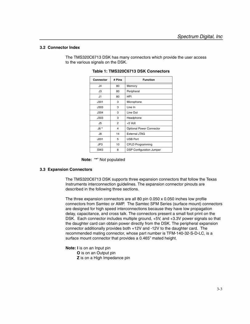
3.2 Connector Index
The TMS320C6713 DSK has many connectors which provide the user accessto the various signals on the DSK.
Note: “*” Not populated
3.3 Expansion Connectors
The TMS320C6713 DSK supports three expansion connectors that follow the TexasInstruments interconnection guidelines. The expansion connector pinouts aredescribed in the following three sections.
The three expansion connectors are all 80 pin 0.050 x 0.050 inches low profileconnectors from Samtec or AMP. The Samtec SFM Series (surface mount) connectorsare designed for high speed interconnections because they have low propagationdelay, capacitance, and cross talk. The connectors present a small foot print on theDSK. Each connector includes multiple ground, +5V, and +3.3V power signals so thatthe daughter card can obtain power directly from the DSK. The peripheral expansionconnector additionally provides both +12V and -12V to the daughter card. Therecommended mating connector, whose part number is TFM-140-32-S-D-LC, is asurface mount connector that provides a 0.465” mated height.
Note: I is on an Input pin O is on an Output pin Z is on a High Impedance pin
Table 1: TMS320C6713 DSK Connectors
Connector # Pins Function
J4 80 Memory
J3 80 Peripheral
J1 80 HPI
J301 3 Microphone
J303 3 Line In
J304 3 Line Out
J303 3 Headphone
J5 2 +5 Volt
J6 * 4 Optional Power Connector
J8 14 External JTAG
J201 5 USB Port
JP3 10 CPLD Programming
SW3 8 DSP Configuration Jumper

Spectrum Digital, Inc
3-4 TMS320VC6713 DSK Module Technical Reference
3.3.1 J4, Memory Expansion Connector
Table 2: J4, Memory Expansion Connector
Pin Signal I/O Description Pin Signal I/O Description
1 5V Vcc 5V voltage supply pin 2 5V Vcc 5V voltage supply pin
3 AEA21 O EMIF address pin 21 4 AEA20 O EMIF address pin 20
5 AEA19 O EMIF address pin 19 6 AEA18 O EMIF address pin 18
7 AEA17 O EMIF address pin 17 8 AEA16 O EMIF address pin 16
9 AEA15 O EMIF address pin 15 10 AEA14 O EMIF address pin 14
11 GND Vss System ground 12 GND Vss System ground
13 AEA13 O EMIF address pin 13 14 AEA12 O EMIF address pin 12
15 AEA11 O EMIF address pin 11 16 AEA10 O EMIF address pin 10
17 AEA9 O EMIF address pin 9 18 AEA8 O EMIF address pin 8
19 AEA7 O EMIF address pin 7 20 AEA6 O EMIF address pin 6
21 5V Vcc 5V voltage supply pin 22 5V Vcc 5V voltage supply pin
23 AEA5 O EMIF address pin 5 24 AEA4 O EMIF address pin 4
25 AEA3 O EMIF address pin 3 26 AEA2 O EMIF address pin 2
27 ABE3# O EMIF byte enable 3 28 ABE2# O EMIF byte enable 2
29 ABE1# O EMIF byte enable 1 30 ABE0# O EMIF byte enable 0
31 GND Vss System ground 32 GND Vss System ground
33 AED31 I/O EMIF data pin 31 34 AED30 I/O EMIF data pin 30
35 AED29 I/O EMIF data pin 29 36 AED28 I/O EMIF data pin 28
37 AED27 I/O EMIF data pin 27 38 AED26 I/O EMIF data pin 26
39 AED25 I/O EMIF data pin 25 40 AED24 I/O EMIF data pin 24
41 3.3V Vcc 3.3V voltage supply pin 42 3.3V Vcc 3.3V voltage supply pin
43 AED23 I/O EMIF data pin 23 44 AED22 I/O EMIF data pin 22
45 AED21 I/O EMIF data pin 21 46 AED20 I/O EMIF data pin 20
47 AED19 I/O EMIF data pin 19 48 AED18 I/O EMIF data pin 18
49 AED17 I/O EMIF data pin 17 50 AED16 I/O EMIF data pin 16
51 GND Vss System ground 52 GND Vss System ground
53 AED15 I/O EMIF data pin 15 54 AED14 I/O EMIF data pin 14
55 AED13 I/O EMIF data pin 13 56 AED12 I/O EMIF data pin 12
57 AED11 I/O EMIF data pin 11 58 AED10 I/O EMIF data pin 10
59 AED9 I/O EMIF data pin 9 60 AED8 I/O EMIF data pin 8
61 GND Vss System ground 62 GND Vss System ground
63 AED7 I/O EMIF data pin 7 64 AED6 I/O EMIF data pin 6
65 AED5 I/O EMIF data pin 5 66 AED4 I/O EMIF data pin 4
67 AED3 I/O EMIF data pin 3 68 AED2 I/O EMIF data pin 2
69 AED1 I/O EMIF data pin 1 70 AED0 I/O EMIF data pin 0
71 GND Vss System ground 72 GND Vss System ground
73 AARE# O EMIF async read enable 74 AAWE# O EMIF async write enable
75 AAOE# O EMIF async output enable 76 AARDY I EMIF asynchronous ready
77 ACE3# O Chip enable 3 78 ACE2# O Chip enable 2
79 GND Vss System ground 80 GND Vss System ground
Spectrum Digital, Inc
3-5
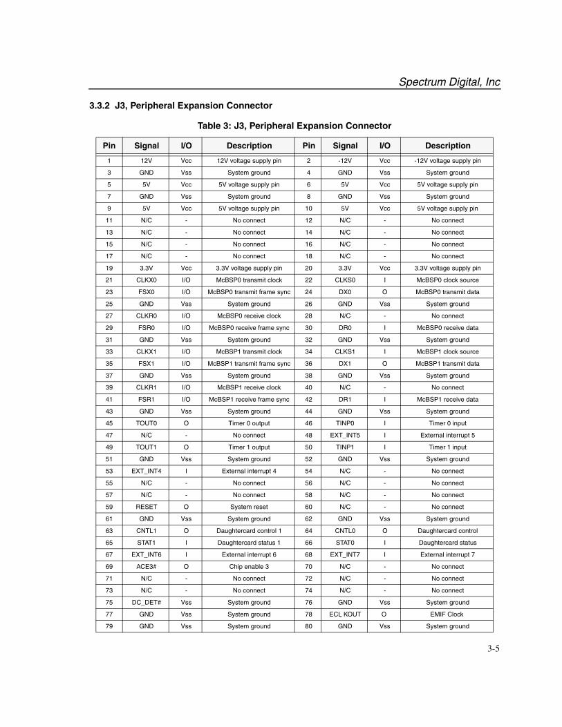
3.3.2 J3, Peripheral Expansion Connector
Table 3: J3, Peripheral Expansion Connector
Pin Signal I/O Description Pin Signal I/O Description
1 12V Vcc 12V voltage supply pin 2 -12V Vcc -12V voltage supply pin
3 GND Vss System ground 4 GND Vss System ground
5 5V Vcc 5V voltage supply pin 6 5V Vcc 5V voltage supply pin
7 GND Vss System ground 8 GND Vss System ground
9 5V Vcc 5V voltage supply pin 10 5V Vcc 5V voltage supply pin
11 N/C - No connect 12 N/C - No connect
13 N/C - No connect 14 N/C - No connect
15 N/C - No connect 16 N/C - No connect
17 N/C - No connect 18 N/C - No connect
19 3.3V Vcc 3.3V voltage supply pin 20 3.3V Vcc 3.3V voltage supply pin
21 CLKX0 I/O McBSP0 transmit clock 22 CLKS0 I McBSP0 clock source
23 FSX0 I/O McBSP0 transmit frame sync 24 DX0 O McBSP0 transmit data
25 GND Vss System ground 26 GND Vss System ground
27 CLKR0 I/O McBSP0 receive clock 28 N/C - No connect
29 FSR0 I/O McBSP0 receive frame sync 30 DR0 I McBSP0 receive data
31 GND Vss System ground 32 GND Vss System ground
33 CLKX1 I/O McBSP1 transmit clock 34 CLKS1 I McBSP1 clock source
35 FSX1 I/O McBSP1 transmit frame sync 36 DX1 O McBSP1 transmit data
37 GND Vss System ground 38 GND Vss System ground
39 CLKR1 I/O McBSP1 receive clock 40 N/C - No connect
41 FSR1 I/O McBSP1 receive frame sync 42 DR1 I McBSP1 receive data
43 GND Vss System ground 44 GND Vss System ground
45 TOUT0 O Timer 0 output 46 TINP0 I Timer 0 input
47 N/C - No connect 48 EXT_INT5 I External interrupt 5
49 TOUT1 O Timer 1 output 50 TINP1 I Timer 1 input
51 GND Vss System ground 52 GND Vss System ground
53 EXT_INT4 I External interrupt 4 54 N/C - No connect
55 N/C - No connect 56 N/C - No connect
57 N/C - No connect 58 N/C - No connect
59 RESET O System reset 60 N/C - No connect
61 GND Vss System ground 62 GND Vss System ground
63 CNTL1 O Daughtercard control 1 64 CNTL0 O Daughtercard control
65 STAT1 I Daughtercard status 1 66 STAT0 I Daughtercard status
67 EXT_INT6 I External interrupt 6 68 EXT_INT7 I External interrupt 7
69 ACE3# O Chip enable 3 70 N/C - No connect
71 N/C - No connect 72 N/C - No connect
73 N/C - No connect 74 N/C - No connect
75 DC_DET# Vss System ground 76 GND Vss System ground
77 GND Vss System ground 78 ECL KOUT O EMIF Clock
79 GND Vss System ground 80 GND Vss System ground

Spectrum Digital, Inc
3-6 TMS320VC6713 DSK Module Technical Reference
3.3.3 J1, HPI Expansion Connector
Table 4: J1, HPI Expansion Connector
Pin Signal I/O Description Pin Signal I/O Description
1 N/C - No connect 2 N/C - No connect
3 GND Vss System ground 4 HPI_RESETn I HPI reset input
5 CLKOUT3 O Clock output3 6 N/C - No connect
7 GND Vss System ground 8 GND Vss System ground
9 HD1/AXR1[7] I/O HPI data 1 10 N/C - No connect
11 HD3/AMUTE1 I/O HPI data 3 12 HD0/AXR1[4] I/O HPI data 0
13 HD5/AHCLKX1 I/O HPI data 5 14 HD2/AFSX1 I/O HPI data 2
15 HD7/GP0[3] I/O HPI data 7 16 HD4/GP0[0] I/O HPI data 4
17 GND Vss System ground 18 HD6/AHCLKR1 I/O HPI data 6
19 HD8/GP0[8] I/O HPI data 8 20 GND Vss System ground
21 HD10/GP0[10] I/O HPI data 10 22 HD9/GP0[9] I/O HPI data 9
23 HD12/GP0[12] I/O HPI data 12 24 HD11/GP0[11] I/O HPI data 11
25 HD14/GP0[14] I/O HPI data 14 26 HD13/GP0[13] I/O HPI data 13
27 GND Vss System ground 28 HD15/GP0[15] I/O HPI data 15
29 HDS2z/AXR1[5] I/O Host data strobe 2 30 GND Vss System ground
31 GND Vss System ground 32 HASz/ACLKX1 I/O Host address strobe
33 HDS1z/AXR1[6] I/O Host data strobe 1 34 GND Vss System ground
35 GND Vss System ground 36 HCNTL0/AXR1[3] I/O Host control 1
37 HCSz/AXR1[2] I/O Host chip select 38 GND Vss System ground
39 GND Vss System ground 40 HHWIL/AFSR1 I/O Host half-word select
41 HCNTL1/AXR1[1] I/O Host control 1 42 GND Vss System ground
43 GND Vss System ground 44 HINTz/GP0[1] I/O Host interrupt
45 HRDYZ/ACLKR1 I/O Host Ready 46 GND Vss System ground
47 GND Vss System ground 48 N/C - No connect
49 HR/Wz/AXR1[0] I/O Host R/W strobe 50 N/C - No connect
51 N/C - No connect 52 N/C - No connect
53 N/C - No connect 54 N/C - No connect
55 N/C - No connect 56 GND Vss System ground
57 N/C - No connect 58 N/C - No connect
59 N/C - No connect 60 N/C - No connect
61 GND Vss System ground 62 N/C - No connect
63 N/C - No connect 64 N/C - No connect
65 N/C - No connect 66 N/C - No connect
67 N/C - No connect 68 SCL0 I/O I2C0 Clock
69 N/C - No connect 70 GND Vss System ground
71 GND Vss System ground 72 SDA0 I/O I2C0 Data
73 N/C - No connect 74 GND Vss System ground
75 GND Vss System ground 76 N/C - No connect
77 N/C - No connect 78 GND Vss System ground
79 GND Vss System ground 80 CLKOUT2/GP0[2] I/O GP I/O 0 bit 2

Spectrum Digital, Inc
3-7
3.4 Audio Connectors
The C6713 DSK has 4 audio connectors. They are described in the followingsections.
3.4.1 J301, Microphone Connector
The input is a 3.5 mm. stereo jack. Both inputs are connected to the microphone so it ismonaural. The signals on the plug are shown in the figure below.
3.4.2 J303, Audio Line In Connector
The audio line in is a stereo input. The input connector is a 3.5 mm stereo jack. Thesignals on the mating plug are shown in the figure below.
Microphone In
Ground
Figure 3-2, Microphone Stereo Jack
Microphone Bias
Left Line In
Ground
Figure 3-3, Audio Line In Stereo Jack
Right Line In
Spectrum Digital, Inc
3-8 TMS320VC6713 DSK Module Technical Reference
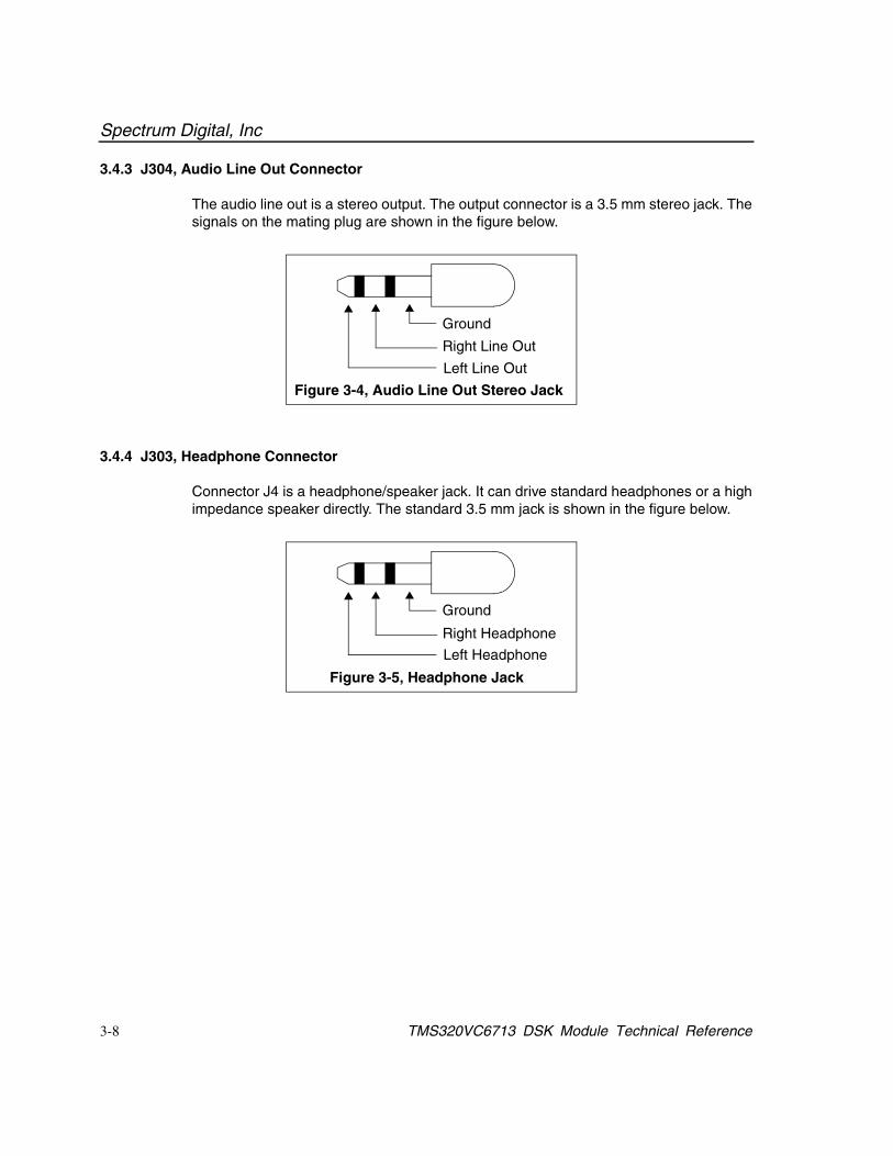
3.4.3 J304, Audio Line Out Connector
The audio line out is a stereo output. The output connector is a 3.5 mm stereo jack. Thesignals on the mating plug are shown in the figure below.
3.4.4 J303, Headphone Connector
Connector J4 is a headphone/speaker jack. It can drive standard headphones or a highimpedance speaker directly. The standard 3.5 mm jack is shown in the figure below.
Left Line Out
Ground
Figure 3-4, Audio Line Out Stereo Jack
Right Line Out
Left Headphone
Ground
Figure 3-5, Headphone Jack
Right Headphone

Spectrum Digital, Inc
3-9
3.5 Power Connectors
The C6713 DSK has 2 power connectors. They are described in the followingsections.
3.5.1 J5, +5 Volt Connector
Power (+5 volts) is brought onto the TMS320C6713 DSK via the J5 connector. Theconnector has an outside diameter of 5.5 mm. and an inside diameter of 2.5 mm. TheA diagram of J5 is shown below.
3.5.2 J6, Optional Power Connector
Connector J6 is an optional power connector. It will operate with the standard personalcomputer power supply. To populate this connector use a Molex #15-24-4041. Thetable below shows the voltages on the respective pins.
Table 5: J6, Optional Power Connector
Pin # Voltage Level
1 +12 Volts
2 -12 Volts
3 Ground
4 +5 Volts
PC Board
J5+5V
Ground
Front ViewFigure 3-6, TMS320C6713 DSK Power Connector
WARNING !Do not plug into J5 and J6 at the same time.
Spectrum Digital, Inc
3-10 TMS320VC6713 DSK Module Technical Reference
3.6 Miscellaneous Connectors
The C6713 DSK has 3 additional connectors to aid the user in developing with thisproduct. They are described in the following sections.
3.6.1 J201, USB Connector
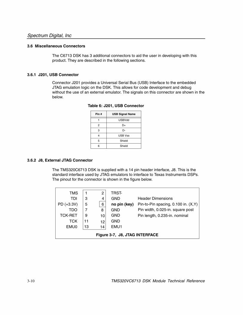
Connector J201 provides a Universal Serial Bus (USB) Interface to the embeddedJTAG emulation logic on the DSK. This allows for code development and debugwithout the use of an external emulator. The signals on this connector are shown in thebelow.
3.6.2 J8, External JTAG Connector
The TMS320C6713 DSK is supplied with a 14 pin header interface, J8. This is thestandard interface used by JTAG emulators to interface to Texas Instruments DSPs.The pinout for the connector is shown in the figure below.
Table 6: J201, USB Connector
Pin # USB Signal Name
1 USBVdd
2 D+
3 D-
4 USB Vss
5 Shield
6 Shield
1 23 4
5 67 89 1011 1213 14
TMSTDI
PD (+3.3V)TDO
TCK-RET
TCKEMU0
TRST-GNDno pin (key)GNDGND
GNDEMU1
Header Dimensions
Pin-to-Pin spacing, 0.100 in. (X,Y)Pin width, 0.025-in. square post
Pin length, 0.235-in. nominal
Figure 3-7, J8, JTAG INTERFACE
Spectrum Digital, Inc
3-11
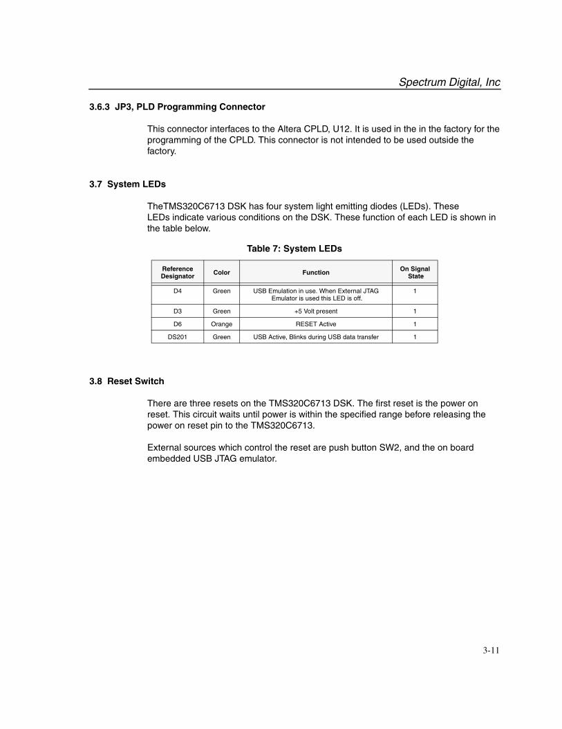
3.6.3 JP3, PLD Programming Connector
This connector interfaces to the Altera CPLD, U12. It is used in the in the factory for theprogramming of the CPLD. This connector is not intended to be used outside thefactory.
3.7 System LEDs
TheTMS320C6713 DSK has four system light emitting diodes (LEDs). TheseLEDs indicate various conditions on the DSK. These function of each LED is shown inthe table below.
3.8 Reset Switch
There are three resets on the TMS320C6713 DSK. The first reset is the power onreset. This circuit waits until power is within the specified range before releasing thepower on reset pin to the TMS320C6713.
External sources which control the reset are push button SW2, and the on boardembedded USB JTAG emulator.
Table 7: System LEDs
Reference Designator Color Function On Signal
State
D4 Green USB Emulation in use. When External JTAG Emulator is used this LED is off.
1
D3 Green +5 Volt present 1
D6 Orange RESET Active 1
DS201 Green USB Active, Blinks during USB data transfer 1

Spectrum Digital, Inc
3-12 TMS320VC6713 DSK Module Technical Reference
A-1
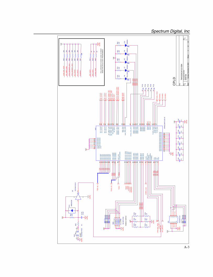
Appendix A
Schematics
This appendix contains the schematics for the TMS320C6713 DSK.Board components with designators over 200 (e.g. DS201, R211) are partof Spectrum Digital’s embedded JTAG emulator and are not included inthese schematics.

Spectrum Digital, Inc
A-2 TMS320C6713 DSK Module Technical Reference
AA
QA
USED
ON
ENGR
-MGR
RLSE
DATE
DATE
REV
SHDA
TE
DATE
REVI
SION
STA
TUS
OF S
HEET
S
REV
SH
DWN
DATE
ENGR
SH
DATE
CHK
MFG
APPL
ICAT
ION
NEXT
ASS
Y
DATE
REV
07-O
ctob
er-2
003
The
TMS
320C
6713
DS
K d
esig
n is
bas
ed o
nTM
S320
C67
13 d
evic
e de
vice
dat
a sh
eet
SPR
S186
B a
nd e
rrat
a S
PR
Z173
E. T
his
sche
mat
ic is
sub
ject
to c
hang
e w
ithou
t not
ificat
ion.
Spe
ctru
m D
igita
l Inc
. ass
umes
no
liabi
lity fo
rap
plic
atio
ns a
ssis
tanc
e, c
usto
mer
pro
duct
des
ign
or in
fring
emen
t of p
aten
ts d
escr
ibed
her
ein.
SP
EC
TRU
M D
IGIT
AL
INC
OR
PO
RAT
ED
12
34
56
7
89
1011
1213
14
CC
AC
AA
B
AB
AA
AA
A
REVI
SION
S
DESC
RIPT
ION
REV
DATE
APPR
OVED
ABE
TA23
-Jan
-200
3
5067
32C
TMS
320C
6713
DSK
B
113
Mon
day,
Nov
embe
r 24,
200
3
Title
Size
Doc
umen
t Num
ber
Rev
Dat
e:S
heet
of
Spectrum Digital, Inc
A-3
CP
LD
PU
LLU
P/D
OW
N T
O K
EEP
LO
GIC
IN R
ESE
TW
HE
N T
HE
CPL
D IS
NO
T P
RO
GR
AM
ME
D.
RE
SE
T
PA
DD
LE S
WIT
CH
5067
32C
TMS
320C
6713
DSK
B
213
Mon
day,
Nov
embe
r 24,
200
3
Title
Size
Doc
umen
t Num
ber
Rev
Dat
e:S
heet
of
US
B_D
SP
_RS
T#
DS
P_R
ST#
DC
_EM
IFA
_OE
#
BR
D_R
ST#
US
ER
_LE
D1
US
ER
_LE
D0
US
ER
_LE
D3
US
ER
_LE
D2
PW
B_R
EV2
PW
B_R
EV1
PW
B_R
EV0
I SR
_TC
KIS
R_T
MS
ISR
_TD
IIS
R_T
DO
PU
SH
B_R
S
TEA2
TEA4
TEA3
TD7
TD6
TD5
TD4
T D3
T D2
TD1
TD0
CP
LD_M
CBS
P0_
MU
X
CP
LD_M
CBS
P1_
MU
X
DC
_STA
T0
DC
_STA
T1
TEA2
1
FLA
SH_P
AGE
FLS
HC
En
SV
S_R
ST#
HP
I_R
ES
ET#
US
B_D
SP
_RS
T#
TD[0
..31]
TCE
3n
TSD
CA
Sn
TSD
RA
Sn
TCE
2n
TSD
WE
n
TEA
[2..2
1]
TCE
1n
DC
_STA
T0D
C_S
TAT1
DC
_CN
TL0
DC
_CN
TL1
DC
_EM
IFA_
OE#
DC
_EM
IFA
_DIR
DC
_CN
TL_O
E#
DC
_RS
T#D
C_D
ET
CPL
D_M
CB
SP1_
MU
XC
PLD
_MC
BSP
0_M
UX
BR
D_R
ST#
DS
P_R
ST#
CO
DE
C_C
LK
FLS
HC
En
FLS
HW
En
FLS
HO
En
FLAS
H_P
AGE
3.3V
DG
ND
3.3V
DG
ND
3.3V
DG
ND
3.3V
3.3V
DG
ND
DG
ND
3.3V
DG
ND
DG
ND
3.3V
DG
ND
3.3V
DG
ND
C68
0.1
C69
0.1
C70
0.1
C39
0.1
C40
0.1
C38
0.1
C71
0.1
C72
0.1
D11 M
MB
D41
48
13R
5610
K
R22
1K
R35
10K
R24
1K
TP16
TP
TP19
TP
TP20
TP
R79
150
R82
150
R81
150
R80
150
U12 EP
M31
28A
TC10
0-10
42 64 41 63 44 45 46 58 40 13 100 98 8
8510 12 90 9 14 35939497
71684767
202329
25 96 75 81 52 37 5 4 79 31 69 83 76 84 80
87 6 36 92 99
39913
3451
82
11263338435359
747886
60 30 48 21
888995
62 15 4 73
18
6566
16 56 61 32 19 1757
DS
P_D
Q0
DS
P_D
Q1
DS
P_D
Q2
DS
P_D
Q3
DS
P_D
Q4
DS
P_D
Q5
DS
P_D
Q6
DS
P_D
Q7
DSP
_AD
DR
0D
SP_A
DD
R1
DSP
_AD
DR
2
DS
P_C
Sn
CPL
D/F
LASH
n
DS
P_R
Sn
DS
P_D
C_C
S0n
DS
P_D
C_C
S1n
DS
P_D
C_W
En
DS
P_D
C_R
En
DS
P_D
C_O
En
US
ER
_SW
0U
SE
R_S
W1
US
ER
_SW
2U
SE
R_S
W3
US
ER
_LE
D0
US
ER
_LE
D1
US
ER
_LE
D2
US
ER
_LE
D3
PW
B_R
EV0
PW
B_R
EV1
PW
B_R
EV2
DC
_STA
T0D
C_S
TAT1
DC
_CN
TL0
DC
_CN
TL1
DC
_DBU
F_D
IRD
C_D
BU
F_O
En
DC
_CN
TL_O
En
DC
_RE
SE
TnD
C_D
ETn
MC
BS
P_S
EL0
MC
BS
P_S
EL1
BR
D_R
Sn
DS
P_R
Sn_
LED
CP
LD_C
LK_O
UT
CLK
INE
MU
_RS
TnP
ON
RS
nP
US
HB
RS
nH
PIR
Sn
VCCINTVCCINTVCCIO
VCCIOVCCIO
VCCIO
GNDGNDGNDGNDGNDGNDGND
GNDGNDGND
SPAR
E0SP
ARE1
SPAR
E2SP
ARE3
GNDGNDGND
TCK
TMS
TDI
TDO
VCCIO
GNDVCCIO
RSV
0R
SV1
RSV
2
FLS
H_C
En
FLSH
_WE
nFL
SH
_OE
n
FLA
SH_P
AGE
R37
NU
R36
1KR33
NU
R53
NU
R34
1K
R54
1K
JP3
HE
ADER
5X21
23
45
67
89
10
RN
19A
10K
RN
19C
10K
RN
19B
10K
D6
YELL
OW
D7
GR
EE
N
D8
GR
EE
N
D9
GR
EE
N
D10
GR
EE
N
U8 SN
74AH
C1G
14
34
52
R83
33C
119
0.1u
F
SW
2
PU
SH
BU
TTO
N
1 234
R84
10K
R23
10K
R40
10K
RN
19D
10K
RN
19E
10K
RN
19F
10K
RN
19G
10K
SW
1
SW D
IP-4
/SM
1234
8765
R78
150
R57
10K
R39
1K
TP10
TP
R98
10K
R97
10K
TP15
TP
Spectrum Digital, Inc
A-4 TMS320C6713 DSK Module Technical Reference
Pla
ce a
ll P
LL e
xter
nal c
ompo
nent
s as
clo
seto
the
DS
P. A
ll P
LL e
xter
nal c
ompo
nent
sm
ust b
e on
a s
ingl
e si
de o
f the
boa
rd.
Max
imiz
e th
e di
stan
ce b
etw
een
switc
hing
sig
nals
an
d th
e P
LL e
xter
nal c
ompo
nent
s.
OPT
ION
AL
5067
32A
TMS
320C
6713
DSK
B
313
Mon
day,
Nov
embe
r 24,
200
3
Title
Size
Doc
umen
t Num
ber
Rev
Dat
e:S
heet
of
DS
P_C
OR
E_C
LK
EIN
T4EI
NT5
EIN
T6EI
NT7
TIN
P0
TIN
P1
TOU
T0TO
UT1
DS
P_T
DO
DS
P_T
RS
T#
DS
P_T
MS
DS
P_TD
I
DS
P_T
CK
DS
P_E
MU
0D
SP
_EM
U1
DS
P_R
ST#
DC
_EIN
T4
DC
_EIN
T6D
C_E
INT7
DC
_TIN
P0
DC
_TIN
P1
DC
_EIN
T5
DC
_TO
UT0
DC
_TO
UT1
DS
P_E
MU
4D
SP
_EM
U5
DS
P_E
MU
2D
SP
_EM
U3
XD
S_4.
1V
DSP
IO_3
.3V
CLK
MO
DE
0
CLK
OU
T2C
LKO
UT3
DG
ND
3.3V
DG
ND
DG
ND
DG
ND
DG
ND
DG
ND
DG
ND
U10
E
TMS
320C
6713
GD
P
D9
B9
D3
B10
C11
B12
A8G1
F1
A3C4
C5
A13
C13 E3
D2
C1
C2
G2 F2 A7 B7 A6 B6
Y11
D10
Y12
EM
U0
EM
U1
EM
U2
EM
U3
EM
U4
EM
U5
TDO
TOU
T0/A
XR
0_2
TOU
T1/A
XR
0_4
CLK
IN
CLK
MO
DE
0
PLL
HV
RE
SE
Tn
NM
I
GP
7/E
XTIN
T7G
P6/
EXT
INT6
GP5
/EX
TIN
T5/A
MU
TEIN
0G
P4/E
XTI
NT4
/AM
UTE
IN1
TIN
P0/A
XR0_
3TI
NP1
/AH
CLK
X0
TDI
TMS
TCK
TRS
Tn
EC
LKIN
CLK
OU
T3C
LKO
UT2
/GP
2
C92
0.1
TP28
E1
EX
CC
ET1
03U
EM
I FIL
TER
13
2
IO
GND
+C
T10
10
C12
1
0.1
C11
30.
01
R77
360
C22
NO
-PO
P
C11
40.
1
R17
NO
-PO
P
U14
50 M
Hz
1 4
8 5
OFF
n
GN
D
VC
C
CLK
L5
Ferr
ite C
hip
R50
33
R25
33R
2633
U21
SN
74C
BTD
3384
PW
1 133 4 7 8 11
2 5 6 9 10
14 17 18 21 22
24 1215 16 19 20 23
1OE
2OE
1A1
1 A2
1A3
1A4
1A5
1B1
1 B2
1B3
1B4
1B5
2A1
2A2
2A3
2A4
2A5
Vcc
GN
D
2B1
2B2
2B3
2B4
2B5
R51
NU
Spectrum Digital, Inc
A-5
FLA
SH
& S
DR
AM
& C
ON
FIG
NEA
R D
SP
256K
x 1
6
2M x
32
MT4
8LC
2M32
B2T
G
4M x
32
MT4
8LC
4M32
B2T
G
JP50
0JP
501
ABAB
BC
BC
RE
V C
AD
DIT
ION
TO
SU
PPO
RT
2MX
32 O
R 4
MX
32
C67
13 R
EQU
IRE
S S
DR
AM M
S A
DD
RE
SS
BIT
SC
ON
NE
CT
TO S
DR
AM B
AN
K B
ITS
. TH
ISD
IFF
ER
S F
RO
M T
HE
C64
xx W
HER
E TH
IS IS
HA
ND
LED
INTE
RN
ALLY
.
5067
32C
TMS
320C
6713
DSK
B
413
Mon
day,
Nov
embe
r 24,
200
3
Title
Size
Doc
umen
t Num
ber
Rev
Dat
e:S
heet
of
TEA
11
TD23
TD22
SDA1
1
T EA
5
TEA
12
TD26
TD21
TD20
TD11
T D9
TD7
TD4
TBE
2n
TEA
3
TD31
TD28
TD27
TEA
4
TD29
TD18
TD3
TEA
8
TD13
TD5
TBE
3n
TBE
1n
TD24
TD1
TD19
TD2
TD15
TD8
TD17
TD25
TD10
SDBA
0TE
A14
TEA
7
TEA
10
TD30
TD16
T EA
6 TBE
0n
TD6
TEA
9
TD12
TEA
2TD
14
TD0
TSD
RA
Sn
TSD
CA
Sn
TSD
WE
n
TCE
0n
TEC
LKO
UT
3.3V
TD11
TD9
TD7
TD4
TD3
TD13
T D5
TD1
TD2
TD15
TD8
TD10
TD6
TD12
TD14
TD0
TEA
2TE
A3
TEA
4TE
A5
TEA
6TE
A7
TEA
8T E
A9
TEA
10TE
A11
TEA
12TE
A13
TEA
14TE
A15
TEA
16TE
A17
TEA
18
TEA
20TE
A19
EA21
EA20
EA19
EA18
EA17
EA16
EA15
EA14
EA13
EA12
EA11
EA10
EA9
EA8
EA7
EA6
EA5
EA4
EA3
EA2
ED0ED1ED2ED3ED4ED5ED6ED7ED8ED9ED10ED11ED12ED13ED14ED15ED16ED17ED18ED19ED20ED21ED22ED23ED24ED25ED26ED27ED28ED29ED30ED31
TEA
21TE
A20
TEA
19TE
A18
TEA
17TE
A16
TEA
15TE
A14
TEA
13TE
A12
TEA
11TE
A10
TEA
9TE
A8
TEA
7TE
A6
TEA
5TE
A4
TEA
3TE
A2
TD0TD1TD2TD3TD4TD5TD6TD7TD8TD9TD10
TD19
TD17
TD14
TD16
TD12
TD18
TD13
TD11
TD15
TD25
TD22
TD29
TD23
TD20
TD24
TD21
TD28TD27TD26
TD31TD30
TCE
0n
ASD
WE#
ASD
RAS
#AS
DC
AS#
ASD
CAS
#
TEC
LKO
UT
3.3V
TEA
13
SD
BA0
SDA1
1
TEA
15
TEA
13TE
A15
TEA
16
BR
D_R
ST#
FLSH
CEn
FLSH
OE
nFL
SHW
En
TAE
CLK
OU
T2 TCE
1nTC
E2n
TCE
3n
TBE
0nTB
E1n
TBE
2nTB
E3n
TSD
WE
nTS
DR
AS
nTS
DC
AS
n
TAR
DY
TD[0
..31]
TEA
[2..2
1]
FLAS
H_P
AGE
3.3V
3.3V
DG
ND
DG
ND
3.3V
3.3V
DG
ND
RN
8A33
R41
1 0K
RN
12F
33
RN
8B33
RN
12G
33
RN
8C33
RN
12H
33
JP50
0
JUM
PE
R3_
SM
T
1
2
3A B C
JP50
1
JUM
PE
R3_
SM
T
1
2
3A B C
RN
8D33
RN
9A33
RN
7B33
RN
7A33
RN
12B
33R
N12
A33
RN
8E33
C97
0.1
RN
9B33
C75
0.1
C73
0.1
RN6F 33
RN6H 33
RN4B 33
RN5F 33RN5E 33RN5D 33
RN5B 33
C95
0.1
RN3C 33
RN3A 33
RN3G 33
RN5C 33
RN4D 33
RN6A 33
RN3D 33
RN6C 33
RN
8F33
RN6G 33
RN4A 33RN5H 33
RN6E 33
RN3E 33
RN6D 33
RN4G 33
RN4C 33
RN4F 33
RN3F 33
RN4H 33
RN4E 33
RN5G 33
RN6B 33
RN3H 33
RN3B 33
RN5A 33
RN
9C33
C74
0.1
C45
0.1
U13
MT4
8LC
4M32
B2T
G-6
2 4 5 7 8 10 11 13 74 76 77 79 80 82 83 85 3 1 34 36 37 39 40 42 45 47 48 5 0 51 53 54 5633
24 66 65 64 63 62 61 60 27 26 2523 22 68 672071 16 19 1 8 1759 2 8 86 72 58 44 84 78 52 46 38 32 12 6
43 29 15 1 81 75 55 49 41 35 9 3
21 70 6973 57 30 14
DQ
0D
Q1
DQ
2D
Q3
DQ
4D
Q5
DQ
6D
Q7
DQ
8D
Q9
DQ
10D
Q11
DQ
12D
Q13
DQ
14D
Q15
DQ
16
DQ
18D
Q19
DQ
20D
Q21
DQ
22D
Q23
DQ
24D
Q25
DQ
26D
Q27
DQ
28D
Q29
DQ
30D
Q31
DQ
17
A10
A9 A8 A7 A6 A5 A4 A3 A2 A1 A0BA1
BA0
CLK
CK
E
CS
DQ
M1
DQ
M0
RAS
CAS
WE
DQ
M3
DQ
M2
VSS
VSS
VSS
VSS
VSS
QV
SSQ
VSS
QV
SSQ
VSS
QV
SSQ
VSS
QV
SSQ
VDD
VDD
VDD
VDD
VDD
QVD
DQ
VDD
QVD
DQ
VDD
QVD
DQ
VDD
QVD
DQ
NC
NC
NC
NC
NC
NC
NC
RN
8G33
RN
9D33
R42
33
RN
8H33
R55
33
RN
9E33
TP5
TPTP
4TP
TP3
TP
RN
9F33
+C
T5 10
R45
33
RN
9G33
U10
A
TMS
320C
6713
GD
P
V5Y4
U19
V20
V6W6
W18
V17
J19
J18
V11
W10
V12
Y10
K18K19L18L19M19M20N18N19N20P18P20R19R20T18T20T19V4W4Y3V2V1U2U1U3T1T2R3R2P1P2P3N3
U18
Y18
W17
Y16V1
6Y
15W
15Y
14W
14V14
W13V1
0Y
9V9Y8
W8V8W7V7Y6
Y5
J17
ABE3
nAB
E2n
ABE1
nAB
E0n
ACE3
nAC
E2n
ACE1
nAC
E0n
BU
SR
EQ
HO
LDA
n
AREn
/SD
CA
Sn/S
SAD
Sn
AO
En/S
DR
ASn
/SSO
En
AWE
n/S
DW
En/S
SWE
n
EC
LKO
UT
ED0ED1ED2ED3ED4ED5ED6ED7ED8ED9
ED10ED11ED12ED13ED14ED15ED16ED17ED18ED19ED20ED21ED22ED23ED24ED25ED26ED27ED28ED29ED30ED31
EA21
EA20
EA19
EA18
EA17
EA16
EA15
EA14
EA13
EA12
EA11
EA10
EA9
EA8
EA7
EA6
EA5
EA4
EA3
EA2
ARD
YH
OLD
n
+C
T13
10
R48
33
R47
33R58
10K
RN
12D
33
RN
7C33
RN
12C
33R
N7D
33
U15
AM29
LV40
0B
2 1 48345678 9
10 13 14
16181920212223242537 462 7
26 28 1 1 1247
1529 31 33 35 38 40 42 44 30 32 34 36 3 9 41 43 4517
A14
A15
A16
A13
A12
A11
A10
A9A8 A19
NC
1N
C2
NC
3
A18
A7A6A5A4A3A2A1A0VC
C
VSS
VSS
CE
OE
WE
RE
SE
T
BY
TE
RY
/BY
DQ
0D
Q1
DQ
2D
Q3
DQ
4D
Q5
DQ
6D
Q7
DQ
8D
Q9
DQ
10D
Q11
DQ
12D
Q13
DQ
14D
Q15
/A-1
A17
RN
9H33
R59
10K
RN
12E
33
Spectrum Digital, Inc
A-6 TMS320C6713 DSK Module Technical Reference
MC
BS
P
5067
32A
TMS
320C
6713
DSK
B
513
Mon
day,
Nov
embe
r 24,
200
3
Title
Size
Doc
umen
t Num
ber
Rev
Dat
e:S
heet
of
DR
1
DX1
FSX1
FSR
1
CLK
R1
CLK
X1
DC
ISO
-4.1
V
CLK
S1
CLK
S0
CLK
R0
DR
0
FSR
0
FSX0
DX0
CLK
X0
DC
_DR
0
DC
_CLK
R0
DC
_CLK
S0
DC
_FSX
0
DC
_CLK
S1
DC
_CLK
R1
DC
_CLK
X1
DC
_DR
1
DC
_FS
R1
DC
_FSX
1
DC
_DX
1
AIC
23S
DA
TAO
UT
AIC
23SD
ATAI
N
BC
LK
LRC
IN
LRC
OU
T
CPL
D_M
CB
SP1_
MU
XC
PLD
_MC
BSP
0_M
UX
CTL
_FSX
0
SC
L0
SDA0
DC
_CLK
X0C
TL_C
LKX
0
DC
_FS
R0
CTL
_DX
0D
C_D
X0
DG
ND
DG
ND
5V
DG
ND
DG
ND
DG
ND
DG
ND
DG
ND
3.3V
R12
360
R27
33
R28
33
U9
SN
74C
BT3
257P
W
4
14
71 1
9 1213 12 15103 5 6
16 8
1A
4B1
2A3B
13A 4A
4B2 S
1B1
OE
3B2
1B2
2B1
2B2
VCC
GN
D
R18
360
U10
D
TMS
320C
6713
GD
P
K 3 H3
G3
J1 H2
J3 H1
E1
M1 L3 M2 L2 M3 L1
N1
N2
CLK
S0/A
HC
LKR
0C
LKR
0/A
CLK
R0
CLK
X0/A
CLK
X0
DR
0/AX
R0_
0D
X0/A
XR0_
1
FSR
0/A
FSR
0FS
X0/A
FSX0
CLK
S/S
CL1
CLK
R1/
AXR
0_6
CLK
X1/
AMU
TE0
DR
1/S
DA
1D
X1AX
R0_
5
FSR
1/AX
R0_
7FS
X1
SC
L0SD
A0
R1
1.6K
D1 LM
4040
DC
IM3-
4.1
21
C28 0.
1
C13 0.
1
R49
10K
R46
10K
R44
10K
R43
10K
U4
SN
74C
BT3
257P
W4
14
71 1
9 1213 12 15103 5 6
16 8
1A
4B1
2A3B
13A 4A
4B2
S1B1
OE
3B2
1B2
2B1
2B2
VCC
GN
D
U1
SN
74C
BT3
257P
W
4
14
711
9 1213 12 15103 5 6
16 8
1A
4B1
2A3B
13A 4A
4B2 S
1B1
OE
3B2
1B2
2B1
2B2
VCC
GN
D
U3
SN
74C
BT3
257P
W4
14
711
9 1213 12 15103 5 6
16 8
1A
4B1
2A3B
13A 4A
4B2
S1B1
OE
3B2
1B2
2B1
2B2
VCC
GN
D

Spectrum Digital, Inc
A-7
HO
ST
PO
RT/
McA
SP
HP
I DAU
GH
TER
CA
RD
CAN
RE
SET
DS
P V
IA T
HIS
SIG
NAL
. SI
GN
AL IS
CO
MB
INE
D W
ITH
OTH
ER
DS
PR
ES
ET
SO
UR
CE
S.
PEN
CIL
SW
ITC
H
END
IAN
BO
OT-
1B
OO
T-0
OFF
- O
PE
NO
N -
CLO
SE
D
iPU
iPU
iPU
iPD
iPU
HPI
_EN
DEV
ICE
CO
NFI
GU
RAT
ION
5067
32A
TMS
320C
6713
DSK
B
613
Mon
day,
Nov
embe
r 24,
200
3
Title
Size
Doc
umen
t Num
ber
Rev
Dat
e:S
heet
of
HD
1H
D3
HD
5H
D7
HD
12H
D14
HD
S2n
HD
S1n
HC
NTL
1
HR
DYn
HR
Wn
HC
Sn
HD
0H
D2
HD
4H
D6
HD
9H
D11
HD
13H
D15
HAS
n
HC
NTL
0
HH
WIL
HIN
Tn
HD
10H
D8
HD
8H
D4
HD
3H
D14
HD
12
HD
15H
D14
HD
13H
D12
HD
11H
D10
HD
9H
D8
HD
7H
D6
HD
5H
D4
HD
3H
D2
HD
1H
D0
HIN
TnH
CN
TL1
HC
NTL
0H
HW
ILH
RW
nH
ASn
HC
Sn
HD
S1n
HR
DYn
HD
S2n
HP
I_R
ES
ET#
CLK
MO
DE
0
CLK
OU
T2
CLK
OU
T3
SC
L0
SD
A0
3.3V
DG
ND
DG
ND
DG
ND3.
3V
R19
10K
R29
1KR
301K
J1 SFM
140L
2SD
LC
12
34
56
78
910
1112
1314
1516
1718
1920
2122
2324
2526
2728
2930
3132
3334
3536
3738
3940
4142
4344
4546
4748
4950
5152
5354
5556
5758
5960
6162
6364
6566
6768
6970
7172
7374
7576
7778
7980
12
34
56
78
910
1112
1314
1516
1718
1920
2122
2324
2526
2728
2930
3132
3334
3536
3738
3940
4142
4344
4546
4748
4950
5152
5354
5556
5758
5960
6162
6364
6566
6768
6970
7172
7374
7576
7778
7980
SW
3
SW D
IP-4
/SM
1 2 3 4
8 7 6 5R
871K
R85
1KR
861K
R3
1 K
U10
C
TMS3
20C
6713
GD
P
B14
C14
A15
C15
A16
B16
C16
B17
A18
C17
B18
C19
C20
D18
D20
E20
H19
F18
E19
F20
E18
G20
H20
G18
G19
J20
HD
15/G
P15
HD
14/G
P14
HD
13/G
P13
HD
12/G
P12
HD
11/G
P11
HD
10/G
P10
HD
9/G
P9H
D8/
GP8
HD
7/G
P3H
D6/
AHC
LKR
1H
D5/
AHC
LKX
1H
D4/
GP0
HD
3/A
MU
TE1
HD
2/A
FSX1
HD
1/AX
R1_
7H
D0/
AXR
1_4
HD
RY
n/AC
LKR
1H
DS2
n/AX
R1_
5H
DS1
n/AX
R1_
6H
CSn
/AXR
1_2
HAS
n/AC
LKX1
HR
Wn/
AXR
1_0
HH
WIL
/AFS
R1
HC
NTL
0/AX
R1_
3H
CN
TL1/
AXR
1_1
HIN
Tn/G
P1

Spectrum Digital, Inc
A-8 TMS320C6713 DSK Module Technical Reference
#OE
DIR
OPE
RA
TIO
NL
L
A
<--
BL
H
A
-->
BH
X
IS
OLA
TIO
N
DA
UG
HTE
RC
AR
D B
UFF
ER
ING
DC
_EM
IFA
_DIR
=1
FOR
WR
ITES
5067
32B
TMS
320C
6713
DSK
B
713
Mon
day,
Nov
embe
r 24,
200
3
Title
Size
Doc
umen
t Num
ber
Rev
Dat
e:S
heet
of
T EA
12
DC
_D30
DC
_D16
DC
_D26
DC
_D14
DC
_D15
DC
_D4
TEA
8
DC
_D10
DC
_D21
DC
_D25
TD17
DC
_A19
TEA
3
TD11
TD1
DC
_A2
TEA
2
TEA
20
TEA
11
TD21
DC
_A16
DC
_D19
DC
_D23
DC
_D3
DC
_A11
DC
_A20
T EA
13
DC
_D24
DC
_D22
DC
_D8
DC
_A8
DC
_A9
TEA
21
DC
_D11
DC
_D17
TEA
9
TD18
TD13
DC
_D6
DC
_D1
DC
_A7
DC
_D20
DC
_A6
TEA
19
TEA
5
DC
_D5
DC
_D0
DC
_A15
TEA
7
TD9
TD15
T EA
14
DC
_D12
DC
_D31
TEA
10D
C_D
7
DC
_D28
TEA
6
DC
_D9
TD24
DC
_D2
DC
_A4
TEA
16
TD16
DC
_A14
DC
_A21
DC
_A3
TEA
18
TD0
DC
_D18
DC
_D27
TEA
17
DC
_A18
DC
_A5
DC
_A10
DC
_A17
TEA
4
TEA
15
TD8
DC
_D13
TD31
DC
_D29
TD2
TD3
TD4
T D5
TD6
TD7
TD14
TD12
TD10 TD
19TD
20
TD22
TD23
TD30
TD29
TD28
TD27
TD26
TD25
DC
_A12
DC
_A13
DC
_A[2
1..2
]
TEA[
2..2
1]
TD[0
..31]
DC
_D[3
1..0
]
TSD
WE
n
TSD
CAS
n
TAE
CLK
OU
T2
TBE
0n
TBE
2n
TCE
3n
TSD
RAS
n
DC
_AR
DY
TCE
2n
TBE
3n
TBE
1nD
C_B
E2#
TAR
DY
DC
_EC
LKO
UT
DC
_BE
3#
DC
_BE
0#D
C_C
E3#
DC
_AW
E#
DC
_AO
E#D
C_A
RE#
DC
_BE
1#
DC
_CE
2#
DC
_CN
TL_O
E#
DC
_EM
IFA_
DIR
DC
_EM
IFA_
OE#
DG
ND
3.3V
DG
ND
3.3V
DG
ND
3.3V
3.3V
3.3V
3.3V 3.
3V
DG
ND
DG
ND
DG
ND
DG
ND
DG
ND
DG
ND
DG
ND
DG
ND
DG
ND
3.3V
DG
ND
3.3V
3.3V
U16
SN
74LV
TH16
245A
7 183142 47 46 44 43 41 40 38 37
2 3 5 6 8 9 11 1236 35 33 32 30 29 27 26
13 14 16 17 19 20 22 23
48 1 25 24 4 10 15 21
28 34 39 45
Vcc
Vcc
Vcc
Vcc
1A1
1A2
1A3
1A4
1A5
1A6
1A7
1A8
1B1
1B2
1B3
1B4
1B5
1B6
1B7
1B8
2A1
2A2
2A3
2A4
2A5
2A6
2A7
2A8
2B1
2B2
2B3
2B4
2B5
2B6
2B7
2B8
1OE
1DIR
2OE
2DIR
GN
DG
ND
GN
DG
ND
GN
DG
ND
GN
DG
ND
R40
31K
U6
SN
74LV
TH16
245A
7 183142 47 46 44 43 41 40 38 37
2 3 5 6 8 9 11 1236 35 33 32 30 29 27 26
13 14 16 17 19 20 22 23
48 1 25 24 4 10 15 21
28 34 39 45
Vcc
Vcc
Vcc
Vcc
1A1
1A2
1A3
1A4
1A5
1A6
1A7
1A8
1B1
1B2
1B3
1B4
1B5
1B6
1B7
1B8
2A1
2A2
2A3
2A4
2A5
2A6
2A7
2A8
2B1
2B2
2B3
2B4
2B5
2B6
2B7
2B8
1OE
1DIR
2OE
2DIR
GN
DG
ND
GN
DG
ND
GN
DG
ND
GN
DG
ND
R15
33
C15
0.1
C17
0.1
C16
0.1
C14
0.1
U17
SN
74LV
TH16
245A
7 183142 47 46 44 43 41 40 38 37
2 3 5 6 8 9 11 1236 35 33 32 3 0 29 27 26
13 14 16 17 1 9 20 22 23
48 1 25 24 4 1 0 15 21
28 3 4 39 45
Vcc
Vcc
Vcc
Vcc
1A1
1A2
1A3
1A4
1A5
1A6
1A7
1A8
1B1
1B2
1B3
1B4
1B5
1B6
1B7
1B8
2A1
2A2
2A3
2A4
2 A5
2A6
2A7
2A8
2B1
2B2
2B3
2B4
2B5
2B6
2B7
2B8
1OE
1DIR
2OE
2DIR
GN
DG
ND
GN
DG
ND
GN
DG
ND
GN
DG
ND
R14
1K
C20
0.1
R13
10K
C19
0.1
C21
0.1
C18
0.1
U5
SN
74LV
TH16
245A
7 183142 47 46 44 43 41 40 38 37
2 3 5 6 8 9 11 1236 35 33 3 2 30 29 27 26
13 14 16 1 7 19 20 22 23
48 1 25 24 4 10 15 21
2 8 34 39 45
Vcc
V cc
V cc
Vcc
1A1
1A2
1A3
1A4
1A5
1A6
1A7
1A8
1B1
1B2
1B3
1B4
1B5
1B6
1B7
1B8
2A1
2A2
2A3
2A4
2A5
2A6
2A7
2A8
2B1
2B2
2B3
2B4
2B5
2B6
2B7
2B8
1OE
1DIR
2OE
2DIR
GN
DG
ND
GN
DG
ND
GN
DG
ND
GN
DG
ND
C96
0.1
C94
0.1
C11
5
0.1
C11
6
0.1
C11
7
0.1
C99
0.1
C98
0.1
C11
8
0.1

Spectrum Digital, Inc
A-9
DA
UG
HTE
RC
AR
D I/
F
Exte
rnal
Mem
ory
Inte
rface
Ext
erna
l Per
iphe
ral I
nter
face
5067
32A
TMS
320C
6713
DSK
B
813
Mon
day,
Nov
embe
r 24,
200
3
Title
Size
Doc
umen
t Num
ber
Rev
Dat
e:S
heet
of
DC
_D27
DC
_D11
DC
_D19
DC
_D9
DC
_A2
DC
_A18
DC
_A12
DC
_D5
DC
_D17
DC
_A14
DC
_A10
DC
_A17
DC
_D15
DC
_A19
DC
_D3
DC
_A21
DC
_D7
DC
_A6
DC
_A16
DC
_D13
DC
_A13
DC
_A3
DC
_D21
DC
_A9
DC
_D29
DC
_D23
DC
_A4
DC
_A5
DC
_A15
DC
_D1
DC
_A7
DC
_A11
DC
_A20
DC
_D25
DC
_A8
DC
_D20
DC
_D4
DC
_D31
DC
_D18
DC
_D22
DC
_D14
DC
_D2
DC
_D30
DC
_D6
DC
_D24
DC
_D26
DC
_D28
DC
_D16
DC
_D10
DC
_D0
DC
_D12
DC
_D8
DC
_DR
0
DC
_CLK
S0
DC
_EIN
T7
DC
_CLK
X0
DC
_CLK
R1
DC
_A[2
1..2
]
DC
_CN
TL0
DC
_BE
3#
DC
_AO
E#D
C_C
E2#
DC
_BE0
#
DC
_CLK
X1
DC
_TO
UT0
DC
_FS
R1
DC
_CN
TL1
DC
_TO
UT1
DC
_RS
T#
DC
_EIN
T4
DC
_AW
E#
DC
_DR
1
DC
_BE
1#
DC
_FS
X1
DC
_EIN
T5
DC
_EC
LKO
UT
DC
_FS
R0
DC
_TIN
P0
DC
_AR
DY
DC
_CLK
S1
DC
_DX0
DC
_FS
X0
DC
_CE
3#
DC
_EIN
T6
DC
_CLK
R0
DC
_D[3
1..0
]
DC
_TIN
P1
DC
_AR
E#
DC
_DX1
DC
_BE2
#
DC
_DE
T
DC
_STA
T1D
C_S
TAT0
DG
ND
DG
ND
DG
ND
DG
ND
- 12V
1 2V
3 .3V
5V
3 .3V
5V
3 .3V
3 .3V
5V5V
3.3V
3.3V
R16
4.7K
R2
0
R65
10K
J4
CO
NN
EC
TOR
40
X 21
23
45
67
89
1011
1213
1415
1617
1819
2021
2223
2425
262 7
2 829
3031
3233
3435
3637
3839
4041
4243
4445
4647
4849
5051
5253
5455
5657
5859
6061
6263
6465
6667
6869
7071
7273
7475
7677
7879
80
12
34
56
78
910
1112
1314
1516
1718
1920
2122
2324
2526
2728
2 93 0
3132
3334
3536
3738
3940
4142
4344
4546
4748
4950
5152
5354
5556
5758
5960
6162
6364
6566
6768
6970
7172
7374
7576
7778
7980
J3
CO
NN
ECTO
R 4
0 X
212
34
56
78
910
1112
1314
1516
1718
1920
2122
2324
2526
2 72 8
2930
3132
3334
3536
3738
3940
4142
4344
4546
4748
4950
5152
5354
5556
5758
5960
6162
6364
6566
6768
6970
7172
7374
7576
7778
7980
12
34
56
78
910
1112
1314
1516
1718
1920
2122
2324
2526
2728
2 93 0
3132
3334
3536
3738
3940
4142
4344
4546
4748
4950
5152
5354
5556
5758
5960
6162
6364
6566
6768
6970
7172
7374
7576
7778
7980

Spectrum Digital, Inc
A-10 TMS320C6713 DSK Module Technical Reference
3.3
sq in
AG
ND
, min
ther
mal
pad
Con
nect
at p
in 1
Set
s Vo
ltage
3.3V
@1.
5Am
p M
ax
3.3
sq in
AG
ND
, min
ther
mal
pad
1.26
V @
1.5A
mp
Max
Con
nect
at p
in 1
WARN
ING:
DO N
OT S
UPPL
Y PO
WER
TO B
OTH
POWE
R CO
NNEC
TORS
AT
THE
SAME
TIM
E!
TO B
E P
OP
ULA
TED
BY
THE
US
ER IF
NE
ED
ED
.
Mol
ex 5
3-10
9-04
10
2.5
MM
JA
CK
POW
ER IN
PUT
DAU
GHT
ERCA
RD
STA
ND
OFF
GR
OUN
DIN
G
KEE
P TR
ACES
A M
INIM
UM
OF
0.07
0 IN
CH
ES
FRO
MTH
ES
E H
OLE
S.
PO
WE
R
EA
CH
REG
ULA
TOR
CA
N S
UP
PLY
UP
TO
3A
OF
CU
RR
ENT.
HO
WE
VER
CO
MP
ON
EN
T V
ALU
ES
HA
VE
BEE
N S
ELE
CTE
D F
OR
1.5
A O
PE
RA
TIO
N.
VA
LUE
S C
ALC
ULA
TED
WIT
H S
WIF
T D
ESIG
N T
OO
L 2.
0.
EM
I S
UP
PR
ESI
ON
. LO
CA
TE N
EAR
EA
CH
RE
GU
LATO
R.
6 V
IAS
FR
OM
PA
D T
O P
LAN
E O
R D
IRE
CT
TIE.
DS
P P
OW
ER M
EAS
UR
EM
EN
TP
OIN
TS.
R IS
251
2 B
OD
Y, 6
VIA
SFR
OM
PA
D T
O P
LAN
E
FOLL
OW
TPS
5431
0 EV
M L
AY
OU
T
1.26
V ->
24.
3K 1
%1.
2V ->
28.
0K 1
%O
PTI
ON
AL C
RO
SS
CO
UPL
E
OP
TIO
NA
L, P
OW
ER
SU
PP
LYLO
AD
RE
SIS
TOR
S, 2
512
BOD
Y
SY
STE
M P
OW
ER
ME
ASU
RE
ME
NT
PO
INT
S.
R IS
251
2 BO
DY,
6 V
IAS
FRO
M P
AD T
O P
LAN
E
0.02
5 O
HM
S F
OR
PO
WER
MEA
SU
RE
ME
NT
0.02
5 O
HM
S F
OR
PO
WE
RM
EAS
UR
EM
EN
T
5067
32B
TMS
320C
6713
DSK
B
913
Mon
day,
Nov
embe
r 24,
200
3
Title
Size
Doc
umen
t Num
ber
Rev
Dat
e:S
heet
of
SE
NSE
_DS
P_C
VD
D
SVS
_RS
T#
DS
PIO
_3.3
V
DS
P_C
VD
D
AG
ND
3.3V
AG
ND
3.3V
5V
-12V
12V
DG
ND
DG
ND
DSP
IO_3
.3V
DS
P_C
VDD
DG
ND
DG
ND
5V
U7
TPS
5431
0PW
P
1 2 3 4 5 6 7 8 9 101112131415161718192021
AGN
DVS
ENSE
CO
MP
PW
RG
DB
OO
T
PH1
PH2
PH3
PH4
PH5
PG
ND
1P
GN
D2
PG
ND
3
VIN
1VI
N2
VIN
3
VBIA
SSS
/EN
AS
YN
CR
TPO
WE
RPA
D
C11
1000
pF
+C
T9
10uF
LE
SR
C64
0.1u
F
C63
0.1u
F
U2
TPS
5431
0PW
P
1 2 3 4 5 6 7 8 9 101112131415161718192021
AGN
DVS
ENSE
CO
MP
PW
RG
DB
OO
T
PH1
PH2
PH3
PH4
PH5
PG
ND
1P
GN
D2
PG
ND
3
VIN
1VI
N2
VIN
3
VBIA
SSS
/EN
AS
YN
CR
TPO
WE
RPA
D
TP32
Test
Poi
nt
1
C4
0.01
uF
L2
BLM
41P
750S
PT
+C
T3
10uF
LE
SR
C7
0.1u
F
C9
0.1u
F
L12.
7 uH
C3
0.04
7uF
C2
560p
FR5
1.65
K 1
%
C5
3300
pFR
810
7 1%
R7 10
K 1
%
+C
T210
0uF
4V
R6
24.3
K 1
%
C1
1000
pF
D12
MU
RS
120T
3
L32.
7 uH
C10
0.04
7uF
C12
7
NO
-PO
P
J 5 RAS
M71
2
CE
NTE
RS
HU
NT
SLE
EVE
C36
8200
pFR
112K
1%
C12
470p
FC
3733
00pF
R20
107
1%
R21
10K
1%
R10
3.74
K 1%
+C
T4
100u
F 4V
R38 10
K
+C
T16
47uF
C65
0.1u
F
R31
71.5
K 1
%
C6
0.1u
F
R9
71.5
K
R66
0
C66
0.03
9uF
JP2
NO
-PO
P
12
JP1
NO
-PO
P
12
R99
0
R4
0
JP4
NO
-PO
P
12
D3
GR
EEN
C8
0.03
9uF
+C
T1
100
uF
+C
T15
100
uF
M1
125_
PH
M3
125_
PHM
212
5_PH
M4
125_
PH
R34
7N
UR
346
NU
TP2
TP
TP31
TP
TP1
TP
L4
BLM
41P
750S
PT
J6
NU
1234
+12
-12
GN
D+5
R52
180
D13
MU
RS
120T
3
D15
MU
RS
120T
3
D14
MU
RS
120T
3
D16
MU
RS
120T
3

Spectrum Digital, Inc
A-11
DS
P P
OW
ER
& D
EC
OU
PLI
NG
All
capa
cito
rs o
n th
is s
heet
are
dec
oupl
ing
capa
cito
rs fo
r the
DS
P. T
hey
shou
ld b
e pl
aced
as
clos
e as
pos
sibl
e to
the
DS
P.
5067
32A
TMS
320C
6713
DSK
B
1013
Mon
day,
Nov
embe
r 24,
200
3
Title
Size
Doc
umen
t Num
ber
Rev
Dat
e:S
heet
of
DS
PIO
_3.3
V
DSP
_CVD
D
DG
ND
DG
ND
DG
ND
DSP
IO_3
.3V
DSP
IO_3
.3V
DS
P_C
VDD
DS
P_C
VDD
DG
ND
DG
ND
DG
ND
DG
ND
C77
0.1
C79
0.1
C51
0.1
C26
0.1
C31
0.1
U10
G
TMS
320C
6713
GD
P
A4 A9 A10
B2 B19
C3
C7
C18 D
5D
6D
11D
14D
15 F4 F17 K1 K4 K17 L4 L17
L20
R4
R17 U
6U
10U
11U
14U
15 V3 V18
W2
W19
CVD
DC
VDD
CVD
DC
VDD
CVD
DC
VDD
CVD
DC
VDD
CVD
DC
VDD
CVD
DC
VDD
CVD
DC
VDD
CVD
DC
VDD
CVD
DC
VDD
CVD
DC
VDD
CVD
DC
VDD
CVD
DC
VDD
CVD
DC
VDD
CVD
DC
VDD
CVD
DC
VDD
CVD
DC
VDD
C41
0.1
C52
0.1
R60
10K
C10
20.
1
C11
00.
1C
880.
1
U10
H
TMS
320C
6713
GD
P
A17
B3
B8
B13
C10 D
1D
16D
19 F3H
18 J2M
18 R1
R18 T3 U
5U
7U
12U
16 V13
V15
V19
W12 Y
7Y
17W3
W9
DV
DD
DV
DD
DV
DD
DV
DD
DV
DD
DV
DD
DV
DD
DV
DD
DV
DD
DV
DD
DV
DD
DV
DD
DV
DD
DV
DD
DV
DD
DV
DD
DV
DD
DV
DD
DV
DD
DV
DD
DV
DD
DV
DD
DV
DD
DV
DD
DV
DD
DV
DD
DV
DD
C78
0.1
C24
0.1
C10
40.
1
U10
I
TMS
320C
6713
GD
P
A1 A2 A11
A14
A19
A20
B1
B4
B15
B20 C
6C
8C
9D
4D
8D
13D
17 E2
E4
E17 F1
9G
4G
17 H4
H17 J4 J9 J1
0J1
1J1
2K
2K
9K
10K
11K
12K
20 L9 L10
L11
L12
M4
M9
M10
M11
M12
M17 N
4N
17 P4
P17
P19
T4 T17
U4
U8
U9
U13
U17
U20
W1
W5
W11
W16
W20
Y1 Y2 Y13
Y19
Y20
VSS
VSS
VSS
VSS
VSS
VSS
VSS
VSS
VSS
VSS
VSS
VSS
VSS
VSS
VSS
VSS
VSS
VSS
VSS
VSS
VSS
VSS
VSS
VSS
VSS
VSS
VSS
VSS
VSS
VSS
VSS
VSS
VSS
VSS
VSS
VSS
VSS
VSS
VSS
VSS
VSS
VSS
VSS
VSS
VSS
VSS
VSS
VSS
VSS
VSS
VSS
VSS
VSS
VSS
VSS
VSS
VSS
VSS
VSS
VSS
VSS
VSS
VSS
VSS
VSS
VSS
VSS
VSS
VSS
C10
30.
1
C25
0.1
C62
0.1
C10
90.
1
C32
0.1
C10
80.
1C
105
0.1
C30
0.1
C58
0.1
C46
0.1
C50
0.1
C90
0.1
C34
0.1
C35
0.1
C10
10.
1
+C
T6 10C
800.
1+
CT8 10
C48
0.1
C56
0.1
+C
T14
10+
CT1
110
C85
0.1
C10
60.
1
C11
20.
1
U10
J
TMS
320C
6713
GD
P
A5 B5
C12 D
7D
12 A12
B11
RSV
RSV
RSV
RSV
RSV
RSV
RSV
C33
0.1
C54
0.1
C47
0.1
C81
0.1
C27
0.1
C23
0.1
C10
00.
1
C83
0.1
C59
0.1
C29
0.1
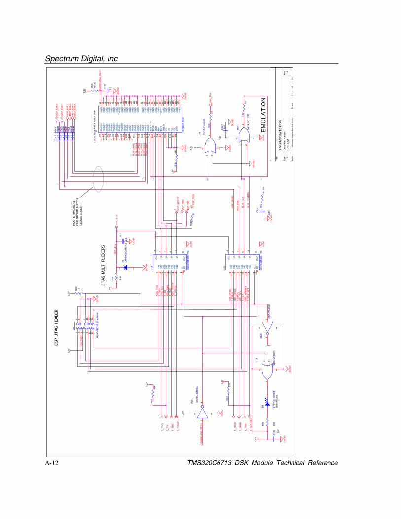
Spectrum Digital, Inc
A-12 TMS320C6713 DSK Module Technical Reference
J TAG
MUL
TIPL
EXER
S
EM
ULA
TIO
N
DSP
JTAG
HEA
DER
ROU
TE T
RAC
ES A
SO
NE
GRO
UP.
MAT
CHSI
GN
AL L
ENG
TH.
LOC
ACTE
R-P
ACK
NEA
R D
SP
US
B IN
US
E
5067
32A
TMS
320C
6713
DSK
B
1113
Mon
day,
Nov
embe
r 24,
200
3
Title
Size
Doc
umen
t Num
ber
Rev
Dat
e:S
heet
of
XD
S_T
RS
T#T_
TMS
XD
S_E
MU
1
XD
S_T
DO
XD
S_T
MS
XD
S_E
MU
0
XD
S_T
VD
XD
S_TD
I
T_E
MU
1
XDS
_4.1
V
T_E
MU
0
HU
RR
ICAN
E_D
ETn
HU
R_E
MU
3H
UR
_EM
U2
HU
R_E
MU
5H
UR
_EM
U4
HU
R_E
MU
1H
UR
_EM
U0
MU
X_E
MU
0
MU
X_EM
U1
HU
R_T
CK
HU
R_T
CK
RTN
T_TR
STn
T_TC
K
HU
RR
ICA
NE
_DE
Tn
XD
S_T
CK
RE
T
XD
S_T
CK
T_TC
K_R
ET
T_TD
O
T_TD
I
DS
P_T
DO
DS
P_TD
I
DS
P_T
MS
T_E
MU
0
T_E
MU
1
DS
P_E
MU
2D
SP
_EM
U3
DS
P_E
MU
5D
SP
_EM
U4
T_TC
K_R
ET
DS
P_E
MU
0
DS
P_E
MU
1
DS
P_T
CK
DS
P_T
RS
T#
T_TM
S
T_TC
K
T_TR
STn
XD
S_4.
1V
T_TD
O
T_TD
I
DG
ND
3.3V
DG
ND
DG
ND
DG
ND
3.3V
DG
ND
5V
DG
ND
DG
ND3.
3V
DG
ND
3.3V
DG
ND
DG
ND
DG
ND
3.3V
3.3V
DG
ND
3.3V
3.3V
DG
ND
DG
ND
3.3V
DG
ND
DG
ND
3.3V
RN
2C42
RN
2D42
U24
SN
74LV
C1G
32
1 24
5 3
R96
33
R92
33
R93
1.6K
D5 LM
4040
DC
IM3-
4.1
21
RN
2B42
RN
2A42
C12
2
.1uF
R10
033
R89
150
U26 SN
74LV
C1G
321 2
4
5 3
R95
100
1%
C12
6
22pF
J8
HE
ADER
7x2
, Em
ulat
ion
1 3 5 7 9
2 4 8 1011
1213
14
R67
47K
R90
47K
C12
4.1
uF
U19
SN
74C
BT3
257P
W4
14
711
9 1213 12 15103 5 6
16 8
1A
4B1
2A3B
13A 4A
4B2
S1B1
OE
3B2
1B2
2B1
2B2
VCC
GN
D
U25
SN
74C
BT3
257P
W4
14
711
9 1213 12 15103 5 6
16 8
1A
4B1
2A3B
13A 4A
4B2
S1B1
OE
3B2
1B2
2B1
2B2
VCC
GN
D
J7 HEA
DE
R 4
x15
A1 A2 A3 A4 A5 A6 A7 A 8 A9 A10
A11
A12
A13
A14
A15
D1
D2
D3
D4
D5
D6
D7
D8
D9
D10
D11
D12
D13
D14
D15
B14
C14
B13
C13
B12
C12
B11
C11
B10
C10B
9C
9
B7
C7
B6
C6
B5
C5
B4
C4
B3
C3
B2
C2
B1
B15C
1C
15 B8
C8
GN
DG
ND
GN
DG
ND
GN
DG
ND
GN
DT Y
PE
0G
ND
GN
DG
ND
GN
DG
ND
GN
DG
ND
GN
DG
ND
GN
DG
ND
GN
DG
ND
GN
DTY
PE
1G
ND
GN
DG
ND
GN
DG
ND
GN
DG
ND
EMU
0EM
U1
EMU
2EM
U3
TCLK
EMU
4EM
U5
EMU
6EM
U7
EMU
8EM
U9
EMU
10
TDO
EMU
11EM
U12
EMU
13EM
U14
EMU
15
TDI
EMU
16EM
U17
TRS
TnTM
S
EMU
18
ID0
ID1
ID2
ID3
TVD
TCK
RTN
D4
LTS
T-C
150G
KT
R94
30.1
K
R88
1K
C12
3
0.1
U23
SN
74LV
C1G
32
1 24
5 3
U22
SN74
AH
C1G
14
3
4
5
2
U18 SN
74AH
C1G
14
3
4
5
2
RN
2H42
RN
2G42
RN
2F42
RN
2E42
R91
1K
C12
5
0.1

Spectrum Digital, Inc
A-13
5 5
4 4
3 3
2 2
1 1
DD
CC
BB
AA
Hie
rarc
hari
cal B
lock
s
5067
32A
TMS
320C
6713
DSK
B
1213
Mon
day,
Nov
embe
r 24,
200
3
Title
Size
Doc
umen
t Num
ber
Rev
Dat
e:S
heet
of
USB
/Em
ulat
ion
USB
/Em
ulat
ion
5V
US
B_D
SP_
RS
T#
T_TD
O
T_TC
KT_
TMS
T_TR
STn
T_E
MU
0T_
EM
U1
T_TD
I
3.3V
PO
NR
Sn
GN
D
T_TC
K_R
ETC
LK_1
2MH
Z
CLK
_24M
HZ
AIC
23 A
udio
AIC
23 A
udio
GN
D
DAT
A_BC
LKD
ATA
_SY
NC
IND
ATA_
DIN
DA
TA_D
OU
T
CTL
_DAT
AC
TL_C
LKC
TL_C
S
CO
DE
C_S
YSC
LK
AIC
3.3V
DA
TA_S
YN
CO
UT
CLK
_12M
HZ
US
B_D
SP_
RS
T#
T_TD
IT _
T MS
T_TC
K
T_EM
U0
T_EM
U1
T_TD
O
SVS
_RS
T#
T _TR
ST n
T_TC
K_R
ET
CTL
_CLK
X0
CTL
_FS
X0
CTL
_DX0
BC
LK
AIC
23SD
ATAO
UT
LRC
OU
T
AIC
23SD
ATAI
NL R
CIN
CO
DE
C_C
LK
5V
DG
ND
3.3V
3.3V
DG
ND
DG
ND
3.3V
DG
ND
U11
SN74
LVC
1G32
1 24
5 3
C67
.1uF
R32
33

Spectrum Digital, Inc
A-14 TMS320C6713 DSK Module Technical Reference

B-1
Appendix B
Mechanical Information
This appendix contains the mechanical information about theTMS320C6713 DSK produced by Spectrum Digital.
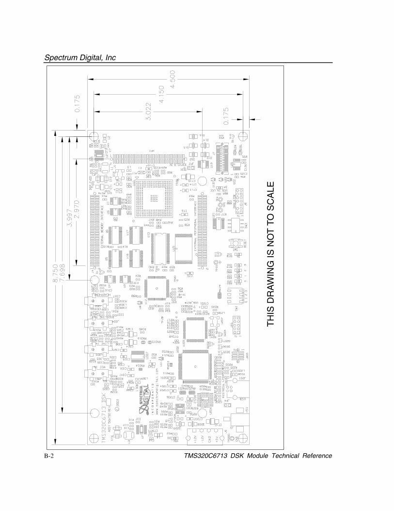
Spectrum Digital, Inc
B-2 TMS320C6713 DSK Module Technical Reference
TH
IS D
RA
WIN
G IS
NO
T T
O S
CA
LE


Printed in U.S.A., November 2003506735-0001 Rev. B