ds1034 - processorpm-powr605 data sheet - … processorpm-powr605 data sheet figure 1....
TRANSCRIPT

www.latticesemi.com 1 DS1034_2.0
April 2015 Data Sheet DS1034
© 2015 Lattice Semiconductor Corp. All Lattice trademarks, registered trademarks, patents, and disclaimers are as listed at www.latticesemi.com/legal. All other brand or product names are trademarks or registered trademarks of their respective holders. The specifications and information herein are subject to change without notice.
Features Precision Programmable Threshold
Monitors, Threshold Accuracy 0.7%• Simultaneously monitors up to six power supplies• Programmable analog trip points (1% step size;
192 steps)• Programmable glitch filter• Power-off detection (75 mV)
Embedded Programmable Timers• Four independent timers• 32 µs to 2 second intervals for timing sequences
Embedded PLD for Logical Control• Rugged 16-macrocell CPLD architecture• 81 product terms / 28 inputs• Implements state machines and combinatorial
functions
Power-Down Mode ICC < 10 µA Digital I/O
• Two dedicated digital inputs• Five programmable digital I/O pins
Wide Supply Range (2.64 V to 3.96 V)• In-system programmable through JTAG• Industrial temperature range: –40 °C to +105 °C• 24-pin QFN package, lead-free option
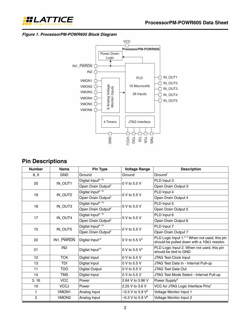
DescriptionLattice’s Power Manager II ProcessorPM-POWR605 is a general-purpose power-supply monitor, reset genera-tor and watchdog timer, incorporating both in-system programmable logic and analog functions implemented in non-volatile E2CMOS® technology. The Proces-sorPM-POWR605 device provides six independent ana-log input channels to monitor power supply voltages. Two general-purpose digital inputs are also provided for miscellaneous control functions.
The ProcessorPM-POWR605 provides up to five open drain digital outputs that can be used for controlling DC-DC converters, low-drop-out regulators (LDOs) and opt-ocouplers, as well as for supervisory and general-pur-pose logic interface functions. The five digital, open drain outputs can optionally be configured as digital inputs to sense more input signals as needed, such as manual reset, etc.
The diagram above shows how a ProcessorPM-POWR605 is used in a typical application. It controls power to the microprocessor system, generates the CPU reset and monitors critical power supply voltages, generating interrupts whenever faults are detected. It also provides a watchdog timer function to detect CPU operating and bus timeout errors.
The ProcessorPM-POWR605 incorporates a 16-macro-cell CPLD. Figure 1 shows the analog input compara-tors and digital inputs used as inputs to the CPLD array. The digital output pins providing the external control sig-nals are driven by the CPLD. Four independently pro-grammable timers also interface with the CPLD and can create delays and time-outs ranging from 32 µs to 2 seconds. The CPLD is programmed using Logi-Builder™, an easy-to-learn language integrated into the PAC-Designer® software. Control sequences are written to monitor the status of any of the analog input channel comparators or the digital inputs.
Application Block Diagram
Voltage Supervisor
ProcessorPM-POWR605
Reset Generator
Watchdog Timer
Power Down
DC-DC#1
DC-DC#2
DC-DC#n
Input Power Supply
Power Up/Down Control
PowerSupply
Bus
CPU /uProcessor
Interrupt –Power Fail
CPU_Reset_in
WDT Trigger
Interrupt – WDT
ManualReset In
ProcessorPM-POWR605In-System Programmable Power Supply Supervisor,
Reset Generator and Watchdog Timer
TM
2
ProcessorPM-POWR605 Data Sheet
Figure 1. ProcessorPM-POWR605 Block Diagram
Pin Descriptions Number Name Pin Type Voltage Range Description
8, 9 GND Ground Ground Ground1
20 IN_OUT1Digital Input9, 10
0 V to 5.5 VPLD Input 3
Open Drain Output2 Open Drain Output 3
19 IN_OUT2Digital Input9, 10
0 V to 5.5 VPLD Input 4
Open Drain Output2 Open Drain Output 4
18 IN_OUT3Digital Input9, 10
0 V to 5.5 VPLD Input 5
Open Drain Output2 Open Drain Output 5
17 IN_OUT4Digital Input9, 10
0 V to 5.5 VPLD Input 6
Open Drain Output2 Open Drain Output 6
15 IN_OUT5Digital Input9, 10
0 V to 5.5 VPLD Input 7
Open Drain Output2 Open Drain Output 7
22 IN1_PWRDN Digital Input10 0 V to 5.5 V3 PLD Logic Input 1.4, 5 When not used, this pin should be pulled down with a 10k resistor.
21 IN2 Digital Input10 0 V to 5.5 V3 PLD Logic Input 2. When not used, this pin should be tied to GND.
12 TCK Digital Input 0 V to 5.5 V JTAG Test Clock Input
13 TDI Digital Input 0 V to 5.5 V JTAG Test Data In - Internal Pull-up
11 TDO Digital Output 0 V to 5.5 V JTAG Test Data Out
14 TMS Digital Input 0 V to 5.5 V JTAG Test Mode Select - Internal Pull-up
3, 16 VCC Power 2.64 V to 3.96 V Power Supply6
10 VCCJ Power 2.25 V to 3.6 V VCC for JTAG Logic Interface Pins7
1 VMON1 Analog Input –0.3 V to 5.9 V8 Voltage Monitor Input 1
2 VMON2 Analog Input –0.3 V to 5.9 V8 Voltage Monitor Input 2
VMON1
VMON2
VMON3
VMON4
VMON5
VMON6
IN1_PWRDN
IN2
VCC
IN_OUT1
IN_OUT2
IN_OUT3
IN_OUT4
IN_OUT5T
MS
TC
K
TD
I
TD
O
VC
CJ
GN
D
PLD
16 Macrocells
28 Inputs
JTAG Interface
6 A
nalo
g V
olta
geM
onito
r In
puts
Power DownLogic
4 Timers
ProcessorPM-POWR605
3
ProcessorPM-POWR605 Data Sheet
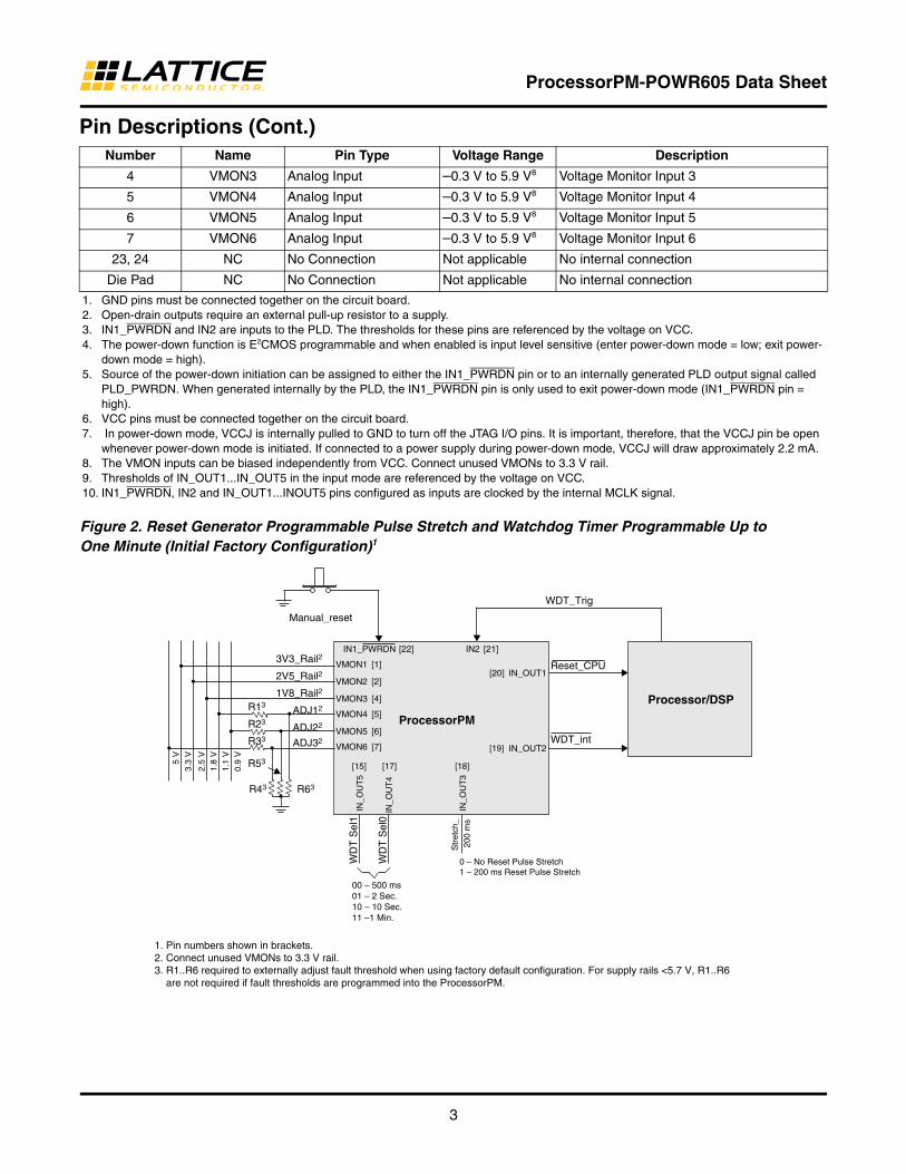
Figure 2. Reset Generator Programmable Pulse Stretch and Watchdog Timer Programmable Up to One Minute (Initial Factory Configuration)1
4 VMON3 Analog Input –0.3 V to 5.9 V8 Voltage Monitor Input 3
5 VMON4 Analog Input –0.3 V to 5.9 V8 Voltage Monitor Input 4
6 VMON5 Analog Input –0.3 V to 5.9 V8 Voltage Monitor Input 5
7 VMON6 Analog Input –0.3 V to 5.9 V8 Voltage Monitor Input 6
23, 24 NC No Connection Not applicable No internal connection
Die Pad NC No Connection Not applicable No internal connection
1. GND pins must be connected together on the circuit board.2. Open-drain outputs require an external pull-up resistor to a supply.3. IN1_PWRDN and IN2 are inputs to the PLD. The thresholds for these pins are referenced by the voltage on VCC.4. The power-down function is E2CMOS programmable and when enabled is input level sensitive (enter power-down mode = low; exit power-
down mode = high).5. Source of the power-down initiation can be assigned to either the IN1_PWRDN pin or to an internally generated PLD output signal called
PLD_PWRDN. When generated internally by the PLD, the IN1_PWRDN pin is only used to exit power-down mode (IN1_PWRDN pin = high).
6. VCC pins must be connected together on the circuit board.7. In power-down mode, VCCJ is internally pulled to GND to turn off the JTAG I/O pins. It is important, therefore, that the VCCJ pin be open
whenever power-down mode is initiated. If connected to a power supply during power-down mode, VCCJ will draw approximately 2.2 mA.8. The VMON inputs can be biased independently from VCC. Connect unused VMONs to 3.3 V rail.9. Thresholds of IN_OUT1...IN_OUT5 in the input mode are referenced by the voltage on VCC.10. IN1_PWRDN, IN2 and IN_OUT1...INOUT5 pins configured as inputs are clocked by the internal MCLK signal.
Pin Descriptions (Cont.)Number Name Pin Type Voltage Range Description
3V3_Rail2
2V5_Rail2
1V8_Rail2
ADJ22
ADJ32
00 – 500 ms01 – 2 Sec.10 – 10 Sec.11 –1 Min.
0 – No Reset Pulse Stretch1 – 200 ms Reset Pulse Stretch
Manual_reset
WDT_Trig
IN_OUT1
IN_OUT2
Processor/DSP
ProcessorPMADJ12
IN_O
UT
5
IN_O
UT
4
VMON1
IN_O
UT
3
5 V
3.3
V
2.5
V1.
8 V
1.1
V0.
9 V
R13
R23
R33
R43 R63
R53
VMON2
VMON3
VMON4
VMON5
VMON6
IN1_PWRDN IN2
[1]
[2]
[4]
[5]
[6]
[7]
[15] [17] [18]
[19]
[20]
[21] [22]
WD
T S
el1
WD
T S
el0
Str
etch
_20
0 m
s
WDT_int
Reset_CPU
1. Pin numbers shown in brackets. 2. Connect unused VMONs to 3.3 V rail.3. R1..R6 required to externally adjust fault threshold when using factory default configuration. For supply rails <5.7 V, R1..R6 are not required if fault thresholds are programmed into the ProcessorPM.

4
ProcessorPM-POWR605 Data Sheet
Absolute Maximum RatingsAbsolute maximum ratings are shown in the table below. Stresses beyond those listed may cause permanent dam-age to the device. Functional operation of the device at these or any other conditions beyond those indicated in the recommended operating conditions of this specification is not implied.
Recommended Operating Conditions
Analog Specifications
Symbol Parameter Conditions Min. Max. Units
VCC Core supply –0.5 4.5 V
VCCJ JTAG logic supply –0.5 6 V
VIN Digital input voltage (all digital I/O pins) –0.5 6 V
VMON VMON input voltage –0.5 6 V
VTRI Voltage applied to tri-stated pins IN_OUT[1:5] –0.5 6 V
TS Storage temperature –65 150 oC
TA Ambient temperature –65 125 oC
ISINKMAX Maximum sink current on any output 23 mA
Symbol Parameter Conditions Min. Max. Units
VCC Core supply voltage at pin 2.64 3.96 V
VCCJ JTAG logic supply voltage at pin 2.25 3.6 V
VIN Input voltage at digital input pins –0.3 5.5 V
VMON Input voltage at VMON pins –0.3 5.9 V
VOUT Open-drain output voltage IN_OUT[1:5] pins –0.3 5.5 V
TAPROGAmbient temperature during programming (Note 1) –40 85 oC
TA Ambient temperature Power applied1 –40 105 oC
TJOP Operating junction temperature Power applied1 –40 108 oC
1. The die pad on the bottom of the QFNS package does not need to be electrically or thermally connected to ground.
Symbol Parameter Conditions Min. Typ. Max. Units
ICC1 Supply current 3.5 5 mA
ICCJ2 Supply current 1 mA
ICC_PWRDN3 Power-down mode supply current ICC + pin leakage currents2 10 µA
1. Includes currents on both VCC pins.2. In power-down mode, VCCJ is internally pulled to GND to turn off the JTAG I/O pins. It is important, therefore, that the VCCJ pin be open
whenever power-down mode is initiated. If connected to a power supply during power-down mode, VCCJ will draw approximately 2.2 mA.3. Leakage measured in power-down mode with applied pin voltages as follows: VCC = 3.96 V; IN1_PWRDN, GND = 0 V; IN2, VMONx and
IN_OUTx = 5.5 V; VCCJ, TDI, TDO, TMS and TCK = open.
5
ProcessorPM-POWR605 Data Sheet
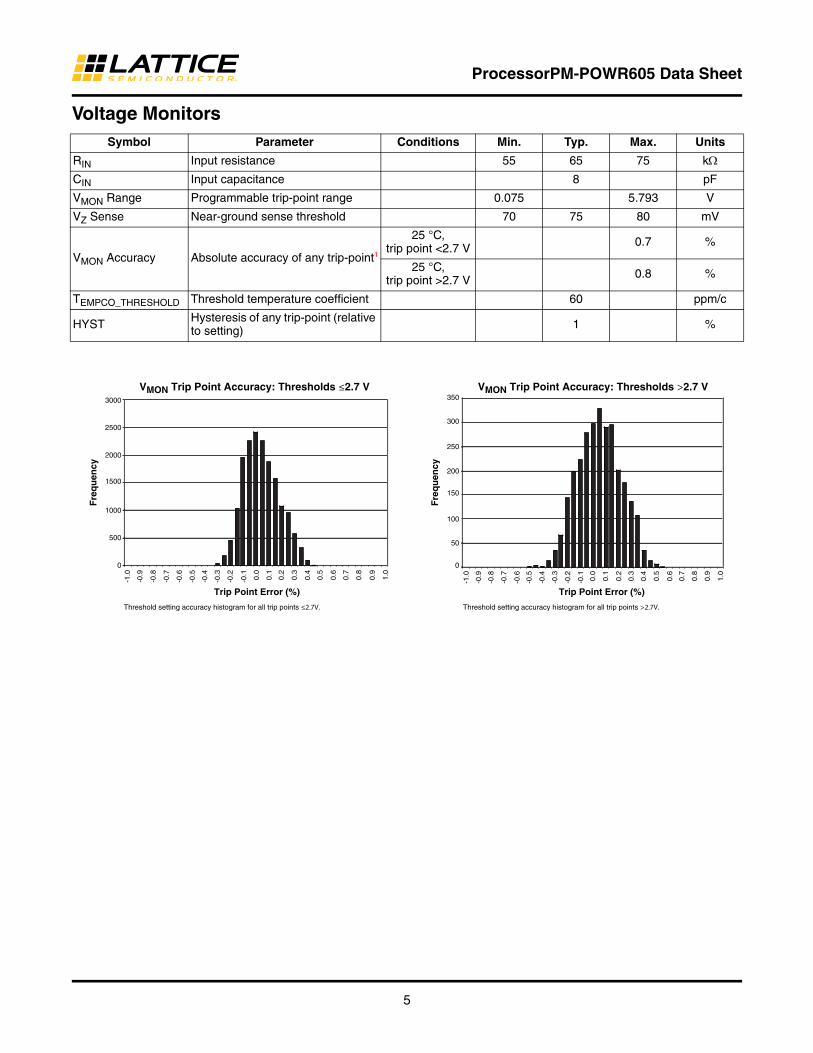
Voltage MonitorsSymbol Parameter Conditions Min. Typ. Max. Units
RIN Input resistance 55 65 75 k
CIN Input capacitance 8 pF
VMON Range Programmable trip-point range 0.075 5.793 V
VZ Sense Near-ground sense threshold 70 75 80 mV
VMON Accuracy Absolute accuracy of any trip-point1
25 °C, trip point <2.7 V 0.7 %
25 °C, trip point >2.7 V 0.8 %
TEMPCO_THRESHOLD Threshold temperature coefficient 60 ppm/c
HYST Hysteresis of any trip-point (relative to setting) 1 %
VMON Trip Point Accuracy: Thresholds ≤2.7 V VMON Trip Point Accuracy: Thresholds >2.7 V 3000
2500
2000
1500
1000
500
Threshold setting accuracy histogram for all trip points ≤2.7V. Threshold setting accuracy histogram for all trip points >2.7V.
0 0
50
100
150
200
250
300
350
Trip Point Error (%)Trip Point Error (%)
Fre
qu
ency
Fre
qu
ency
-1.0
-0.9
-0.8
-0.7
-0.6
-0.5
-0.4
-0.3
-0.2
-0.1 0.0
0.1
0.2
0.3
0.4
0.5
0.6
0.7
0.8
0.9
1.0
-1.0
-0.9
-0.8
-0.7
-0.6
-0.5
-0.4
-0.3
-0.2
-0.1 0.0
0.1
0.2
0.3
0.4
0.5
0.6
0.7
0.8
0.9
1.0

6
ProcessorPM-POWR605 Data Sheet
Power-On Reset (Internal)
Figure 3. Internal Power-On Reset
Symbol Parameter Conditions Min. Typ. Max. Units
TRST Delay from VTH to start-up state 100 µs
TSTART Duration of start-up state 300 µs
TBROMinimum duration brown out required to enter reset state 1 5 µs
TPOR Delay from brown out to reset state 7 µs
VTL Threshold below which POR is LOW1 2.2 V
VTH Threshold above which POR is HIGH1 2.5 V
VT Threshold above which POR is valid1 0.8 V
1. Corresponds to VCC supply voltage.
VCC
VT
VTL
VTH
POR (Internal)
VMONs Ready (Internal)
TSTART
PLDCLK (Internal)
ResetState
AnalogCalibration
TRST
TBRO
Start Up State
TPOR
7
ProcessorPM-POWR605 Data Sheet
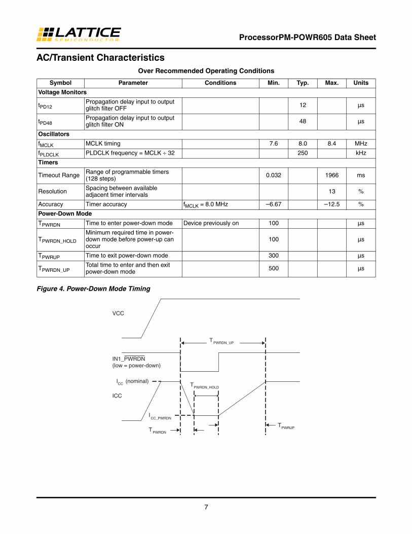
AC/Transient CharacteristicsOver Recommended Operating Conditions
Figure 4. Power-Down Mode Timing
Symbol Parameter Conditions Min. Typ. Max. Units
Voltage Monitors
tPD12Propagation delay input to output glitch filter OFF 12 µs
tPD48Propagation delay input to output glitch filter ON 48 µs
Oscillators
fMCLK MCLK timing 7.6 8.0 8.4 MHz
fPLDCLK PLDCLK frequency = MCLK 32 250 kHz
Timers
Timeout Range Range of programmable timers (128 steps) 0.032 1966 ms
Resolution Spacing between available adjacent timer intervals 13 %
Accuracy Timer accuracy fMCLK = 8.0 MHz –6.67 –12.5 %
Power-Down Mode
TPWRDN Time to enter power-down mode Device previously on 100 µs
TPWRDN_HOLD
Minimum required time in power-down mode before power-up can occur
100 µs
TPWRUP Time to exit power-down mode 300 µs
TPWRDN_UPTotal time to enter and then exit power-down mode 500 µs
IN1_PWRDN(low = power-down)
VCC
ICC
T PWRDN
TPWRUP
T PWRDN_UP
ICC_PWRDN
ICC (nominal)TPWRDN_HOLD

8
ProcessorPM-POWR605 Data Sheet
Digital SpecificationsOver Recommended Operating Conditions
Figure 5. ProcessorPM Digital Output, VOL vs. ISINK Characteristics
Symbol Parameter Conditions Min. Typ. Max. Units
IIL,IIH Input leakage, no pull-up/pull-down +/-10 µA
IPU Input pull-up current (TMS, TDI) 70 µA
VIL Voltage input, logic low1
TDI, TMS, TCK, IN[1:2], IN_OUT[1:5]2, VCCJ = 3.3 V supply
0.8V
TDI, TMS, TCK,VCCJ = 2.5 V supply 0.7
VIH Voltage input, logic high1
TDI, TMS, TCK, IN[1:2], IN_OUT[1:5]2, VCCJ = 3.3 V supply
2.0V
TDI, TMS, TCK, VCCJ = 2.5 V supply 1.7
VOLIN_OUT[1:5]3 ISINK = 20 mA 0.8
VTDO ISINK = 4 mA 0.4
VOH TDO ISRC = 4 mA VCC - 0.4 V
ISINKOutput sink current per digital output IN_OUT[1:5]
VOL < 0.8 V 20 mA
Chip powered down, out-puts pulled up to 3.6 V <1 µA
ISINKTOTAL4 All digital outputs 67 mA
1. IN_OUT[1:5], IN[1:2] referenced to VCC; TDO, TDI, TMS, and TCK referenced to VCCJ.2. When configured as inputs.3. When configured as open drain outputs.4. Sum of maximum current sink from all digital outputs combined. Reliable operation is not guaranteed if this value is exceeded.
0
5
10
15
20
25
30
35
40
0 0.2 0.4 0.6 0.8 1.0
VOL (V)
I SIN
K (
mA
)

9
ProcessorPM-POWR605 Data Sheet
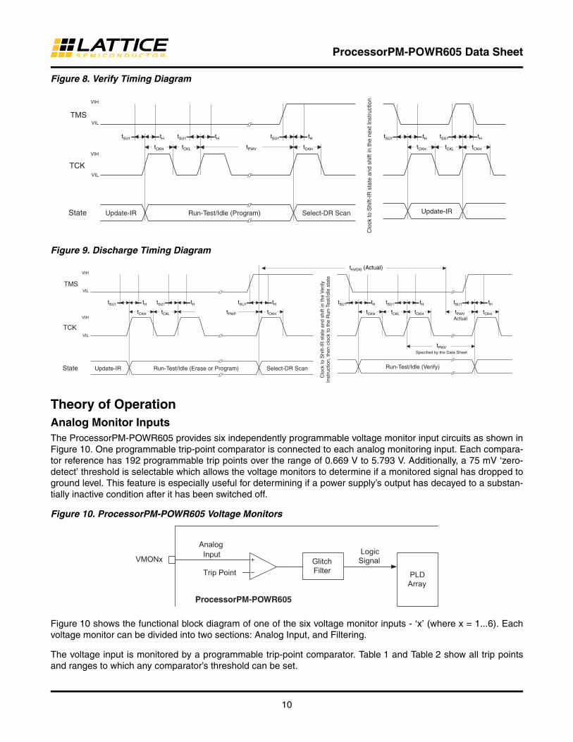
Timing for JTAG Operations
Figure 6. Erase (User Erase or Erase All) Timing Diagram
Figure 7. Programming Timing Diagram
Symbol Parameter Conditions Min. Typ. Max. Units
tISPEN Program enable delay time 10 — — µs
tISPDIS Program disable delay time 30 — — µs
tHVDIS High voltage discharge time, program 30 — — µs
tHVDIS High voltage discharge time, erase 200 — — µs
tCEN Falling edge of TCK to TDO active — — 10 ns
tCDIS Falling edge of TCK to TDO disable — — 10 ns
tSU1 Setup time 5 — — ns
tH Hold time 10 — — ns
tCKH TCK clock pulse width, high 20 — — ns
tCKL TCK clock pulse width, low 20 — — ns
fMAX Maximum TCK clock frequency — — 25 MHz
tCO Falling edge of TCK to valid output — — 10 ns
tPWV Verify pulse width 30 — — µs
tPWP Programming pulse width 20 — — ms
VIH
VIL
VIH
VIL
Update-IR Run-Test/Idle (Erase) Select-DR Scan
Clo
ck to
Shi
ft-IR
sta
te a
nd s
hift
in th
e D
isch
arge
In
stru
ctio
n, th
en c
lock
to th
e R
un-T
est/I
dle
stat
e
Run-Test/Idle (Discharge)
Specified by the Data Sheet
TMS
TCK
State
tH tH tH tH tH tH tSU1 tSU1 tSU1 tSU1 tSU1 tSU1
tSU2
tCKH tCKH tCKH tCKH tCKH tGKL tGKL
TMS
TCK
State
VIH
VIL
VIH
VI L
Update-IR Run-Test/Idle (Program) Select-DR Scan
Clo
ck to
Shi
ft-IR
sta
te a
nd s
hift
in th
e ne
xt
Inst
ruct
ion,
whi
ch w
ill s
top
the
disc
harg
e pr
oces
s
Update-IR
tSU1 tSU1 tSU1 tSU1 tSU1 tH tH tH tH tH
tCKL tPWP tCKH tCKH tCKH tCKH tCKL
10
ProcessorPM-POWR605 Data Sheet
Figure 8. Verify Timing Diagram
Figure 9. Discharge Timing Diagram
Theory of OperationAnalog Monitor InputsThe ProcessorPM-POWR605 provides six independently programmable voltage monitor input circuits as shown in Figure 10. One programmable trip-point comparator is connected to each analog monitoring input. Each compara-tor reference has 192 programmable trip points over the range of 0.669 V to 5.793 V. Additionally, a 75 mV ‘zero-detect’ threshold is selectable which allows the voltage monitors to determine if a monitored signal has dropped to ground level. This feature is especially useful for determining if a power supply’s output has decayed to a substan-tially inactive condition after it has been switched off.
Figure 10. ProcessorPM-POWR605 Voltage Monitors
Figure 10 shows the functional block diagram of one of the six voltage monitor inputs - ‘x’ (where x = 1...6). Each voltage monitor can be divided into two sections: Analog Input, and Filtering.
The voltage input is monitored by a programmable trip-point comparator. Table 1 and Table 2 show all trip points and ranges to which any comparator’s threshold can be set.
TMS
TCK
State
VIH
VIL
VIH
VIL
Update-IR Run-Test/Idle (Program) Select-DR Scan
Clo
ck to
Shi
ft-IR
sta
te a
nd s
hift
in th
e ne
xt In
stru
ctio
n
Update-IR
tH tH tH tH tH
tCKH tCKH tCKH tCKL tPWV tCKH tCKL
tSU1 tSU1 tSU1 tSU1 tSU1
TMS
TCK
State
VIH
VIL
VIH
VIL
Update-IR Run-Test/Idle (Erase or Program)
Select-DR Scan
Clo
ck to
Shi
ft-IR
sta
te a
nd s
hift
in th
e V
erify
In
stru
ctio
n, th
en c
lock
to th
e R
un-T
est/I
dle
stat
e
Run-Test/Idle (Verify)
Specified by the Data Sheet
Actual
tH tH tH tH tH tH tSU1
tCKH
tHVDIS (Actual)
tCKH tCKH tCKH tCKL tPWP tPWV tCKH tCKL
tPWV
tSU1 tSU1 tSU1 tSU1 tSU1
LogicSignal
AnalogInputVMONx
Trip PointGlitchFilter PLD
Array
ProcessorPM-POWR605
11
ProcessorPM-POWR605 Data Sheet
Each comparator outputs a HIGH signal to the PLD array if the voltage at its positive terminal (VMONx pin) is greater than its programmed trip point setting, otherwise it outputs a LOW signal.
A hysteresis of approximately 1% of the setpoint is provided by the comparators to reduce false triggering as a result of input noise. The hysteresis provided by the voltage monitor is a function of the input divider setting. Table 3 lists the typical hysteresis versus voltage monitor trip-point.
Programmable Over-Voltage and Under-Voltage ThresholdsFigure 11 (a) shows the power supply ramp-up and ramp-down voltage waveforms. Because of hysteresis, the comparator outputs change state at different thresholds depending on the direction of excursion of the monitored power supply.
Figure 11. (a) Power Supply Voltage Ramp-up and Ramp-down Waveform and the Resulting Comparator Output, (b) Corresponding to Upper and Lower Trip Points
During power supply ramp-up the comparator output changes from logic 0 to 1 when the power supply voltage crosses the upper trip point (UTP). During ramp down the comparator output changes from logic state 1 to 0 when the power supply voltage crosses the lower trip point (LTP). To monitor for over voltage fault conditions, the UTP should be used. To monitor under-voltage fault conditions, the LTP should be used.
Table 1 and Table 2 show both the under-voltage and over-voltage trip points, which are automatically selected in software depending on whether the user is monitoring for an over-voltage condition or an under-voltage condition.
UTP
LTP
Mon
itore
d P
ower
Sup
ply
Vot
lage
Comparator Logic Output
(a)
(b)

12
ProcessorPM-POWR605 Data Sheet
Table 1. Trip Point Table Used For Over-Voltage Detection (in Volts)
Table 2. Trip Point Table Used For Under-Voltage Detection (in Volts)
REF/MON F E D C B A 9 8 7 6 5 4
1F 0.799 0.952 1.134 1.349 1.597 1.904 2.266 2.690 3.189 3.795 4.864 5.793
1E 0.791 0.943 1.122 1.335 1.581 1.885 2.243 2.664 3.156 3.756 4.814 5.734
1D 0.783 0.933 1.111 1.321 1.565 1.866 2.220 2.636 3.123 3.718 4.764 5.675
1C 0.775 0.923 1.099 1.308 1.548 1.847 2.196 2.608 3.091 3.679 4.715 5.615
1B 0.767 0.913 1.088 1.294 1.532 1.827 2.173 2.581 3.059 3.640 4.665 5.556
1A 0.758 0.904 1.076 1.280 1.516 1.808 2.150 2.553 3.026 3.601 4.615 5.497
19 0.750 0.894 1.065 1.266 1.499 1.788 2.127 2.526 2.994 3.562 4.566 5.438
18 0.743 0.884 1.053 1.252 1.484 1.769 2.103 2.498 2.961 3.524 4.516 5.379
17 0.735 0.874 1.041 1.240 1.468 1.749 2.081 2.471 2.928 3.485 4.467 5.320
16 0.727 0.865 1.030 1.226 1.451 1.730 2.058 2.444 2.896 3.446 4.417 5.261
15 0.718 0.855 1.018 1.212 1.435 1.710 2.035 2.416 2.864 3.407 4.367 5.201
14 0.710 0.845 1.007 1.198 1.419 1.691 2.012 2.389 2.831 3.369 4.318 5.143
13 0.702 0.836 0.995 1.184 1.402 1.671 1.988 2.361 2.798 3.330 4.268 5.083
12 0.694 0.826 0.983 1.171 1.386 1.652 1.965 2.333 2.766 3.291 4.218 5.025
11 0.686 0.816 0.972 1.157 1.370 1.632 1.942 2.306 2.733 3.252 4.169 4.965
10 0.678 0.806 0.960 1.143 1.353 1.614 1.919 2.279 2.700 3.214 4.119 4.906
REF/MON F E D C B A 9 8 7 6 5 4
1F 0.791 0.943 1.122 1.335 1.581 1.885 2.243 2.664 3.156 3.756 4.814 5.734
1E 0.783 0.933 1.111 1.321 1.565 1.866 2.220 2.636 3.123 3.718 4.764 5.675
1D 0.775 0.923 1.099 1.308 1.548 1.847 2.196 2.608 3.091 3.679 4.715 5.615
1C 0.767 0.913 1.088 1.294 1.532 1.827 2.173 2.581 3.059 3.640 4.665 5.556
1B 0.758 0.904 1.076 1.280 1.516 1.808 2.150 2.553 3.026 3.601 4.615 5.497
1A 0.750 0.894 1.065 1.266 1.499 1.788 2.127 2.526 2.994 3.562 4.566 5.438
19 0.743 0.884 1.053 1.252 1.484 1.769 2.103 2.498 2.961 3.524 4.516 5.379
18 0.735 0.874 1.041 1.240 1.468 1.749 2.081 2.471 2.928 3.485 4.467 5.320
17 0.727 0.865 1.030 1.226 1.451 1.730 2.058 2.444 2.896 3.446 4.417 5.261
16 0.718 0.855 1.018 1.212 1.435 1.710 2.035 2.416 2.864 3.407 4.367 5.201
15 0.710 0.845 1.007 1.198 1.419 1.691 2.012 2.389 2.831 3.369 4.318 5.143
14 0.702 0.836 0.995 1.184 1.402 1.671 1.988 2.361 2.798 3.330 4.268 5.083
13 0.694 0.826 0.983 1.171 1.386 1.652 1.965 2.333 2.766 3.291 4.218 5.025
12 0.686 0.816 0.972 1.157 1.370 1.632 1.942 2.306 2.733 3.252 4.169 4.965
11 0.678 0.806 0.960 1.143 1.353 1.614 1.919 2.279 2.700 3.214 4.119 4.906
10 0.669 0.797 0.949 1.129 1.337 1.594 1.895 2.252 2.669 3.175 4.069 4.847

13
ProcessorPM-POWR605 Data Sheet
Table 3. Comparator Hysteresis vs. Trip-Point
The second section in the ProcessorPM-POWR605’s input voltage monitor is a digital filter. When enabled, the comparator output will be delayed by a filter time constant of 48 µs, and is especially useful for reducing the possi-bility of false triggering from noise that may be present on the voltages being monitored. When the filter is disabled, the comparator output will be delayed by 12 µs. In both cases, enabled or disabled, the filters also provide synchro-nization of the input signals to the PLD clock. This synchronous sampling feature effectively eliminates the possibil-ity of race conditions from occurring in any subsequent logic that is implemented in the ProcessorPM-POWR605’s internal PLD logic.
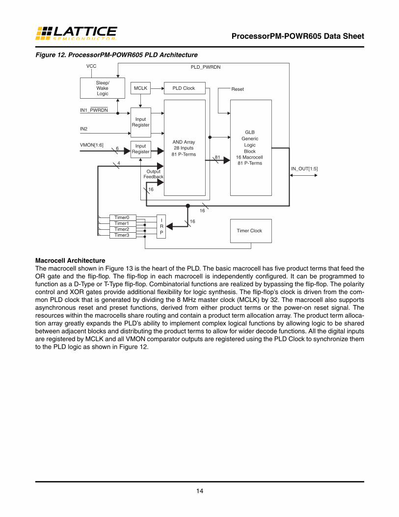
PLD BlockFigure 12 shows the ProcessorPM-POWR605 PLD architecture, which is derived from Lattice’s ispMACH® 4000 CPLD. The PLD architecture allows flexibility in designing various state machines and control functions for power supply management. The AND array has 28 inputs and generates 81 product terms. The product terms are fed into a single logic block made up of 16 macrocells. The output signals of the ProcessorPM-POWR605 device are derived from the PLD as shown in Figure 12.
Trip-point Range (V)
Hysteresis (mV)Low Limit High Limit
0.669 0.799 8
0.797 0.952 10
0.949 1.134 12
1.129 1.349 14
1.337 1.597 17
1.594 1.904 19
1.895 2.266 23
2.252 2.690 28
2.669 3.189 33
3.175 3.795 39
4.069 4.864 50
4.847 5.793 60
75 mV 0 (Disabled)
14
ProcessorPM-POWR605 Data Sheet
Figure 12. ProcessorPM-POWR605 PLD Architecture
Macrocell ArchitectureThe macrocell shown in Figure 13 is the heart of the PLD. The basic macrocell has five product terms that feed the OR gate and the flip-flop. The flip-flop in each macrocell is independently configured. It can be programmed to function as a D-Type or T-Type flip-flop. Combinatorial functions are realized by bypassing the flip-flop. The polarity control and XOR gates provide additional flexibility for logic synthesis. The flip-flop’s clock is driven from the com-mon PLD clock that is generated by dividing the 8 MHz master clock (MCLK) by 32. The macrocell also supports asynchronous reset and preset functions, derived from either product terms or the power-on reset signal. The resources within the macrocells share routing and contain a product term allocation array. The product term alloca-tion array greatly expands the PLD’s ability to implement complex logical functions by allowing logic to be shared between adjacent blocks and distributing the product terms to allow for wider decode functions. All the digital inputs are registered by MCLK and all VMON comparator outputs are registered using the PLD Clock to synchronize them to the PLD logic as shown in Figure 12.
Reset
OutputFeedback
16
VMON[1:6]6
Timer1Timer0
Timer2Timer3
IRP Timer Clock
16
PLD ClockMCLK
4
16
IN2
AND Array28 InputsInput
Register
InputRegister
81 P-Terms
Sleep/WakeLogic
IN1_PWRDN
VCC
GLBGenericLogicBlock
16 Macrocell81 P-Terms
81
PLD_PWRDN
IN_OUT[1:5]

15
ProcessorPM-POWR605 Data Sheet
Figure 13. ProcessorPM-POWR605 Macrocell Block Diagram
Clock and Timer FunctionsFigure 14 shows a block diagram of the ProcessorPM-POWR605’s internal clock and timer systems. The master clock operates at a fixed frequency of 8MHz, from which a fixed 250kHz PLD clock is derived.
Figure 14. Clock and Timer System
The internal oscillator runs at a fixed frequency of 8 MHz. This signal is used as a source for the PLD and timer clocks. It is also used for clocking the comparator outputs and clocking the digital filters in the voltage monitor cir-cuits.
A divide-by-32 prescaler divides the internal 8MHz oscillator down to 250 kHz for the PLD clock and for the pro-grammable timers. Each of the four timers provides independent timeout intervals ranging from 32 µs to 1.96 sec-onds in 128 steps.
PT0
PT1
PT2
PT3
PT4
D/T Q
R P To PLD Output
CLK
Clock
Polarity
Macrocell flip-flop provides D, T, or combinatorial
output with polarity
Product Term Allocation
Power On Reset
Global Polarity Fuse for Init Product Term
Block Init Product Term
InternalOscillator
8MHz32
Timer 0
Timer 1
Timer 3
Timer 2
PLD Clock
To/From PLD

16
ProcessorPM-POWR605 Data Sheet
Digital Inputs and Optional Device Power DownThe ProcessorPM-POWR605 has two dedicated digital input pins which are registered by MCLK as shown in Figure 12, then connected to to the input AND array of the PLD (IN[1:2]). The pins are standard CMOS inputs and are referenced to VCC.
The optional power-down mode is a programmable feature controlled via the IN1_PWRDN pin. It is used to power-down the ProcessorPM-POWR605 and power it up again as desired. When in power-down mode, the Proces-sorPM-POWR605 draws a minimal amount of supply current (less than 10µA max). The device is brought out of power-down mode by applying a logic high signal on the level sensitive IN1_PWRDN pin.
When it exits power-down mode, the ProcessorPM-POWR605 is internally reset to its initial power-on state before resuming normal operation. The logic and limited memory needed to “wakeup” on cue are all that remain on during power-down mode. Other functions and capabilities such as voltage monitoring and PLD logic states are all lost when the ProcessorPM-POWR605 is in power-down mode. Open drain outputs go into Hi-Z mode and all digital inputs, except IN1_PWRDN, stop responding to logic input signals.
There are two E2CMOS bits associated with the ProcessorPM-POWR605 power-down function. Configuring these bits for specific power-down functionality is achieved using PAC-Designer, a software design tool for Lattice pro-grammable mixed signal devices. Table 4 is a truth table detailing the operation of the ProcessorPM-POWR605 power-down logical control function.
Table 4. PWRDN Truth Table1
To use the ProcessorPM-POWR605’s power-down function, the E2CMOS PWRDN enable bit must be set during initial device design configuration. Power-down is disabled otherwise (the initial default).
When power is first applied to ProcessorPM-POWR605, the device checks to see if a power-down condition exists, and then if it is already present will proceed immediately to the power-down state. During the brief period that the device is on, it will consume full power but it will proceed directly to power-down mode without executing any state machine instructions, etc. This time to initially detect the power-down command and then shut down is given in the power-down specifications section of the data sheet.
In addition to the IN1_PWRDN pin, Table 4 shows how an alternate signal from the PLD called PLD_PWRDN can be used to initiate power-down (not the default). This can be useful when power-down is the last step in a series of ProcessorPM-POWR605 PLD controlled states, such as turning off supplies in sequence or acknowledging pro-cessor signals, etc.
Note: The only way to exit power-down mode, regardless of how it is initiated, is with the IN1_PWRDN pin. Apply-ing a logic high to IN1_PWRDN will always return the ProcessorPM-POWR605 to normal operation. Finally, whenever the ProcessorPM-POWR605 is in power-down mode, VCCJ is internally pulled to GND to turn off the JTAG I/O pins. It is important, therefore, that the VCCJ pin be open when power-down mode is initiated. If con-nected to a power supply during power-down mode, VCCJ will draw approximately 2.2 mA.
IN1_PWRDN Input Pin
PLD_PWRDN Internal Signal
PWRDN Enable Bit PWRDN Source Bit Power Mode
X X Clear X Normal
1 X Set X Normal
0 X Set IN1_PWRDN Pin Power-down
0 0 Set Internal Signal PLD_PWRDN Power-down
1. When in power-down mode, the ProcessorPM-POWR605 will not respond to logic inputs (except to the IN1_PWRDN pin) and all outputs will be high impedance.
17
ProcessorPM-POWR605 Data Sheet
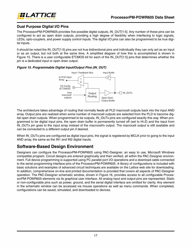
Dual Purpose Digital I/O PinsThe ProcessorPM-POWR605 provides five possible digital outputs, IN_OUT[1:5]. Any number of these pins can be configured to act as open drain outputs, providing a high degree of flexibility when interfacing to logic signals, LEDs, opto-couplers, and power supply control inputs. The digital I/O pins can also be programmed to be true digi-tal inputs.
It should be noted the IN_OUT[1:5] pins are not true bidirectional pins and individually they can only act as an input or as an output, but not both at the same time. A simplified diagram of how this is accomplished is shown in Figure 15. There is a user configurable E2CMOS bit for each of the IN_OUT[1:5] pins that determines whether the pin is a dedicated input or open drain output.
Figure 15. Programmable Digital Input/Output Pins (IN_OUT)
The architecture takes advantage of routing that normally feeds all PLD macrocell outputs back into the input AND array. Output pins are realized when some number of macrocell outputs are selected from the PLD to become dig-ital open drain outputs. When programmed to be outputs, IN_OUTx pins are configured exactly this way. When pro-grammed to be digital input pins, the open drain buffer is permanently turned off (set to Hi-Z) and the input from IN_OUTx pin goes to the input array instead of the macrocell’s output. The macrocell output is still available and can be connected to a different output pin if desired.
When IN_OUTx pins are configured as digital input pins, the signal is registered by MCLK prior to going to the input AND array, the same as the IN1 and IN2 digital inputs.
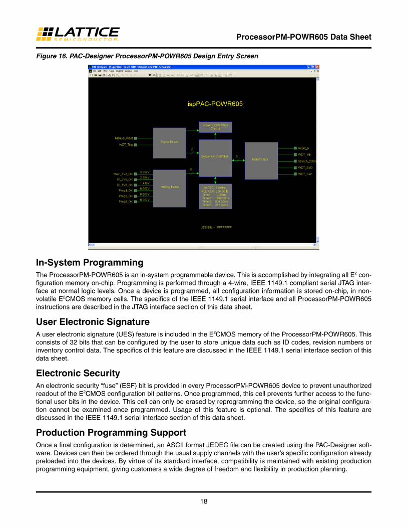
Software-Based Design EnvironmentDesigners can configure the ProcessorPM-POWR605 using PAC-Designer, an easy to use, Microsoft Windows compatible program. Circuit designs are entered graphically and then verified, all within the PAC-Designer environ-ment. Full device programming is supported using PC parallel port I/O operations and a download cable connected to the serial programming interface pins of the ProcessorPM-POWR605. A library of configurations is included with basic solutions and examples of advanced circuit techniques are available on the Lattice web site for downloading. In addition, comprehensive on-line and printed documentation is provided that covers all aspects of PAC-Designer operation. The PAC-Designer schematic window, shown in Figure 16, provides access to all configurable Proces-sorPM-POWR605 elements via its graphical user interface. All analog input and output pins are represented. Static or non-configurable pins such as power, ground, and the serial digital interface are omitted for clarity. Any element in the schematic window can be accessed via mouse operations as well as menu commands. When completed, configurations can be saved, simulated, and downloaded to devices.
frommacrocell
outputs
10
Open DrainOutput Buffer
Input Buffer
to PLD InputArray
IN_OUTx
Input / Feedback Mux
OutputRouting
I/O Config(E 2CMOS)
18
ProcessorPM-POWR605 Data Sheet
Figure 16. PAC-Designer ProcessorPM-POWR605 Design Entry Screen
In-System ProgrammingThe ProcessorPM-POWR605 is an in-system programmable device. This is accomplished by integrating all E2 con-figuration memory on-chip. Programming is performed through a 4-wire, IEEE 1149.1 compliant serial JTAG inter-face at normal logic levels. Once a device is programmed, all configuration information is stored on-chip, in non-volatile E2CMOS memory cells. The specifics of the IEEE 1149.1 serial interface and all ProcessorPM-POWR605 instructions are described in the JTAG interface section of this data sheet.
User Electronic SignatureA user electronic signature (UES) feature is included in the E2CMOS memory of the ProcessorPM-POWR605. This consists of 32 bits that can be configured by the user to store unique data such as ID codes, revision numbers or inventory control data. The specifics of this feature are discussed in the IEEE 1149.1 serial interface section of this data sheet.
Electronic SecurityAn electronic security “fuse” (ESF) bit is provided in every ProcessorPM-POWR605 device to prevent unauthorized readout of the E2CMOS configuration bit patterns. Once programmed, this cell prevents further access to the func-tional user bits in the device. This cell can only be erased by reprogramming the device, so the original configura-tion cannot be examined once programmed. Usage of this feature is optional. The specifics of this feature are discussed in the IEEE 1149.1 serial interface section of this data sheet.
Production Programming SupportOnce a final configuration is determined, an ASCII format JEDEC file can be created using the PAC-Designer soft-ware. Devices can then be ordered through the usual supply channels with the user’s specific configuration already preloaded into the devices. By virtue of its standard interface, compatibility is maintained with existing production programming equipment, giving customers a wide degree of freedom and flexibility in production planning.

19
ProcessorPM-POWR605 Data Sheet
Initial Factory ConfigurationProcessorPM devices are shipped preconfigured with a 6-supply reset generator and a programmable watchdog timer application. This section describes the implemented functions in detail.
Figure 17 shows the functional block diagram implemented in the factory-configured ProcessorPM device.
Figure 17. Initial Factory Configuration Functional Block Diagram
The output of the 6-supply voltage monitor block will switch to logic 1 when all six supply-rail voltages are above their respective threshold settings. Each of the voltage monitoring inputs is filtered with a 48 microsecond glitch fil-ter. All six glitch filter outputs are connected to a 6-input AND gate. The AND gate output is connected to a 200 ms pulse stretch block. The user may or may not bypass the 200ms pulse stretch block via multiplexer selection. When the Stretch_200ms signal is at logic 0, the output of the 6-input AND gate is routed directly to the D-FF. When the Stretch_200ms signal is at Logic 1, the output of the 200 ms Pulse Stretch block is routed to the D-FF. The D-FF is clocked by an internally-generated 250 kHz signal and is reset when the manual reset input is activated. The Reset_CPU signal is active low, that is, logic 0, when any supply is less than its threshold or when the manual reset
3.3 V-5%
200 ms Pulse Stretch
D-FF
Stretch_200ms
0
1
Reset_CPU
50 ms Debounce
Manual_reset
Rst
250 kHz
500 ms WDT
2-Sec WDT
10-Sec WDT
1-Min WDT
WDT_Trig
WDT Reset
00
01
10
11
WDT_Sel1 WDT_Sel0
WDT_int
ProcessorPM3V3_Rail
2V5_Rail
1V8_Rail
ADJ1
ADJ2
ADJ3
Glitch Filter
+
–
2.5 V-5%
+
–
1.8 V-5%
+
–
0.669 V
+
–
0.669 V
+
–
0.669 V
+
–
AND
Glitch Filter
Glitch Filter
Glitch Filter
Glitch Filter
Glitch Filter

20
ProcessorPM-POWR605 Data Sheet
input is active. Reset_CPU is logic 1 when all supplies are above their respective thresholds and the manual reset input is inactive. When Reset_CPU is active the watchdog timer is held in the reset state.
During the operation, one can directly reset the output using the Manual_reset pin. The Manual_reset signal is an active low input. The 50 ms de-bounce circuit block filters glitches less than 50 ms and the filtered signal is used to reset the D-FF. Minimum pulse width of the manual reset input is 50 ms.
The ProcessorPM design provides a watchdog timer with 4 pin-selectable timer delay settings. The watchdog tim-ers are triggered by the falling edge of the WDT_Trig signal. Minimum pulse width of the WDT_Trig signal is 10 microseconds. The WDT_Sel1 and WDT_Sel0 signals are used to select the Watchdog timer delay. Table 5 shows the watchdog timer delay setting corresponding to WDT_Sel1 and WDT_Sel0 inputs.
Table 5. Programmable Watchdog Timer Delay Selection
When the delay between successive WDT_Trig falling edge signals exceeds the watchdog timer delay setting, a 6-microsecond-wide low-going pulse is generated on the WDT_int pin. After generating the output pulse, the watch-dog timer is restarted. It continues to generate 6-microsecond pulses regularly at watchdog delay set intervals until a falling edge of WDT_Trig signal is received. Watchdog timers start after the Reset_CPU signal is deactivated.
The following timing waveform shows WDT_int signal after the watchdog timer expiry. Note the minimum watchdog Trigger pulse width is 10 microseconds. The watchdog timer gets retriggered only by the falling edge of the WDT_Trig signal.
Figure 18. Watchdog Timer Interrupt Gerneration Timing
The watchdog timer delay can be dynamically changed before the current watchdog timer elapse time is exceeded in order to provide for a longer startup delay, for example. However, any changes made to WDT_Sel1 and WDT_Sel0 must be done within 400 ms of either the rising edge of Reset_CPU or the falling edge of WDT_Trig. For example, WDT_Sel1 and WDT_Sel0 might initially be set to 0x10 for a power-up delay of 10 seconds and then after the system is up and running WDT_Sel1 and WDT_Sel0 might be modified to 0x00 to enable a shorter watch-dog delay of 500 ms. The change in the WDT_Sel1 and WDT_Sel0 bits must be made within 400 ms of a WDT_Trig pulse to alter the current WDT delay time. If the change occurs after the 400 ms window, the current WDT delay time is not guaranteed.
WTD_Sel1 WDT_Sel0 Watchdog Timer Delay (Typ.)
0 0 500 ms
0 1 2 sec.
1 0 10 sec.
1 1 1 min.
6 µs (typ.)
10 µs (min.)
WDT Delay Time
WDT_Trig
WDT_int

21
ProcessorPM-POWR605 Data Sheet
Programmable Reset GeneratorThe integrated reset generator activates (Active low) the Reset_CPU signal (Figure 2) when any of the six supplies are less than their fault level. When all supplies are stable and the pulse stretch function is enabled the Reset_CPUsignal will be deactivated after 200 ms.
Voltage threshold setting:
• VMON1 to VMON3 thresholds are set to 3.3 V - 5%, 2.5 V - 5% and 1.8 V - 5% respectively
• VMON4 to VMON6 thresholds are set at 0.669 V. These VMON inputs can be used to monitor supply rails from 0.669 V to 24 V or higher using external resistor-based potential dividers. The resistor values are calculated using the formula shown in Figure 19.
• When monitoring fewer than six supplies, all unused VMON inputs should be connected to 3.3 V rail.
Figure 19. Setting Fault Threshold Using External Resistors for VMON4, VMON5 and VMON6
Programmable Reset Pulse StretchingSome reset generator functions require that the reset pulse be held active for an extended period of time after the supplies are stabilized. One can introduce a 200 ms pulse stretch by connecting the Stretch_200ms pin to 3.3 V. If the Stretch_200ms pin is grounded the reset pulse stretch function will be disabled.
Manual_reset InputWhen the Manual_reset input is pulled low, the Reset_CPU gets activated immediately. When the reset input is released, the reset output also gets released. The Manual_reset input is debounced with a 50 ms timer.
Figure 20. Reset_CPU Signal Responding to Manual_reset
ProcessorPM devices are factory preconfigured to integrate a programmable 6-supply reset generator (configured through pin strapping) and a programmable watchdog timer. See Figure 21.
R1 = R2 *((VRAIL * (1-F/100))
VT-1)
VRAIL – Monitored Supply Rail Voltage
F – Supply Fault Tolerance level in %
VT – VMON Threshold setting = 0.669 V
Note: This equation assumes that R2 ≤ 3 kOhm
VT - Internal Threshold0.669V
VMON4..6R1
R2
VRAIL
ProcessorPM
ADJx
50 ms
ContactBounce
ContactBounce
Manual_reset
Reset_CPU

22
ProcessorPM-POWR605 Data Sheet
Figure 21. Reset Generator Programmable Pulse Stretch and Watchdog Timer Programmable Up to One Minute (Initial Factory Configuration)1
IEEE Standard 1149.1 Interface (JTAG)Serial Port Programming Interface Communication with the ProcessorPM-POWR605 is facilitated via an IEEE 1149.1 test access port (TAP). It is used by the ProcessorPM-POWR605 as a serial programming interface. A brief description of the ProcessorPM-POWR605 JTAG interface follows. For complete details of the reference specifica-tion, refer to the publication, Standard Test Access Port and Boundary-Scan Architecture, IEEE Std 1149.1-1990 (which now includes IEEE Std 1149.1a-1993).
OverviewAn IEEE 1149.1 test access port (TAP) provides the control interface for serially accessing the digital I/O of the Pro-cessorPM-POWR605. The TAP controller is a state machine driven with mode and clock inputs. Given in the cor-rect sequence, instructions are shifted into an instruction register, which then determines subsequent data input, data output, and related operations. Device programming is performed by addressing the configuration register, shifting data in, and then executing a program configuration instruction, after which the data is transferred to inter-nal E2CMOS cells. It is these non-volatile cells that store the configuration or the ProcessorPM-POWR605. A set of instructions are defined that access all data registers and perform other internal control operations. For compatibil-ity between compliant devices, two data registers are mandated by the IEEE 1149.1 specification. Others are func-tionally specified, but inclusion is strictly optional. Finally, there are provisions for optional data registers defined by the manufacturer. The two required registers are the bypass and boundary-scan registers. Figure 22 shows how the instruction and various data registers are organized in an ProcessorPM-POWR605.
3V3_Rail2
2V5_Rail2
1V8_Rail2
ADJ22
ADJ32
00 – 500 ms01 – 2 Sec.10 – 10 Sec.11 –1 Min.
0 – No Reset Pulse Stretch1 – 200 ms Reset Pulse Stretch
Manual_reset
WDT_Trig
IN_OUT1
IN_OUT2
Processor/DSP
ProcessorPMADJ12
IN_O
UT
5
IN_O
UT
4
VMON1
IN_O
UT
3
5 V
3.3
V
2.5
V1.
8 V
1.1
V0.
9 V
R13
R23
R33
R43 R63
R53
VMON2
VMON3
VMON4
VMON5
VMON6
IN1_PWRDN IN2
[1]
[2]
[4]
[5]
[6]
[7]
[15] [17] [18]
[19]
[20]
[21] [22]
WD
T S
el1
WD
T S
el0
Str
etch
_20
0 m
s
WDT_int
Reset_CPU
1. Pin numbers shown in brackets. 2. Connect unused VMONs to 3.3 V rail.3. R1..R6 required to externally adjust fault threshold when using factory default configuration. For supply rails <5.7 V, R1..R6 are not required if fault thresholds are programmed into the ProcessorPM.

23
ProcessorPM-POWR605 Data Sheet
Figure 22. ProcessorPM-POWR605 TAP Registers
TAP Controller SpecificsThe TAP is controlled by the Test Clock (TCK) and Test Mode Select (TMS) inputs. These inputs determine whether an Instruction Register or Data Register operation is performed. Driven by the TCK input, the TAP consists of a small 16-state controller design. In a given state, the controller responds according to the level on the TMS input as shown in Figure 23. Test Data In (TDI) and TMS are latched on the rising edge of TCK, with Test Data Out (TDO) becoming valid on the falling edge of TCK. There are six steady states within the controller: Test-Logic-Reset, Run- Test/Idle, Shift-Data-Register, Pause-Data-Register, Shift-Instruction-Register and Pause-Instruction-Register. But there is only one steady state for the condition when TMS is set high: the Test-Logic-Reset state. This allows a reset of the test logic within five TCKs or less by keeping the TMS input high. Test-Logic-Reset is the power-on default state.
ADDRESS REGISTER (61 BITS)
E2CMOS NON-VOLATILE
MEMORY
UES REGISTER (32 BITS)
IDCODE REGISTER (32 BITS)
BYPASS REGISTER (1 BIT)
INSTRUCTION REGISTER (8 BITS)
TEST ACCESS PORT (TAP)LOGIC
OUTPUTLATCH
TDI TCK TMS TDO
MU
LTIP
LEX
ER
DATA REGISTER (81 BITS)

24
ProcessorPM-POWR605 Data Sheet
Figure 23. TAP States
When the correct logic sequence is applied to the TMS and TCK inputs, the TAP will exit the Test-Logic-Reset state and move to the desired state. The next state after Test-Logic-Reset is Run-Test/Idle. Until a data or instruction shift is performed, no action will occur in Run-Test/Idle (steady state = idle). After Run-Test/Idle, either a data or instruc-tion shift is performed. The states of the Data and Instruction Register blocks are identical to each other differing only in their entry points. When either block is entered, the first action is a capture operation. For the Data Regis-ters, the Capture-DR state is very simple: it captures (parallel loads) data onto the selected serial data path (previ-ously chosen with the appropriate instruction). For the Instruction Register, the Capture-IR state will always load the IDCODE instruction. It will always enable the ID Register for readout if no other instruction is loaded prior to a Shift-DR operation. This, in conjunction with mandated bit codes, allows a “blind” interrogation of any device in a compliant IEEE 1149.1 serial chain. From the Capture state, the TAP transitions to either the Shift or Exit1 state. Normally the Shift state follows the Capture state so that test data or status information can be shifted out or new data shifted in. Following the Shift state, the TAP either returns to the Run-Test/Idle state via the Exit1 and Update states or enters the Pause state via Exit1. The Pause state is used to temporarily suspend the shifting of data through either the Data or Instruction Register while an external operation is performed. From the Pause state, shifting can resume by reentering the Shift state via the Exit2 state or be terminated by entering the Run-Test/Idle state via the Exit2 and Update states. If the proper instruction is shifted in during a Shift-IR operation, the next entry into Run-Test/Idle initiates the test mode (steady state = test). This is when the device is actually programmed, erased or verified. All other instructions are executed in the Update state.
Test InstructionsLike data registers, the IEEE 1149.1 standard also mandates the inclusion of certain instructions. It outlines the function of three required and six optional instructions. Any additional instructions are left exclusively for the manu-facturer to determine. The instruction word length is not mandated other than to be a minimum of two bits, with only the BYPASS and EXTEST instruction code patterns being specifically called out (all ones and all zeroes respec-tively). The ProcessorPM-POWR605 contains the required minimum instruction set as well as one from the optional instruction set. In addition, there are several proprietary instructions that allow the device to be configured and verified. Table 6 lists the instructions supported by the ProcessorPM-POWR605 JTAG Test Access Port (TAP)
Test-Logic-Rst
Run-Test/Idle Select-DR-Scan Select-IR-Scan
Capture-DR Capture-IR
Shift-DR Shift-IR
Exit1-DR Exit1-IR
Pause-DR Pause-IR
Exit2-DR Exit2-IR
Update-DR Update-IR
1
0
0 0
0 0
0 0
1 1
0 0
0 0
1 1
1 1
0 0 1 1
0 0
1 1
1 1
1 1 1 0
Note: The value shown adjacent to each state transition in this figure represents the signal present at TMS at the time of a rising edge at TCK.

25
ProcessorPM-POWR605 Data Sheet
controller:
Table 6. ProcessorPM-POWR605 TAP Instruction Table
BYPASS is one of the three required instructions. It selects the Bypass Register to be connected between TDI and TDO and allows serial data to be transferred through the device without affecting the operation of the Proces-sorPM-POWR605. The IEEE 1149.1 standard defines the bit code of this instruction to be all ones (11111111).
The required SAMPLE/PRELOAD instruction dictates the Boundary-Scan Register be connected between TDI and TDO. The ProcessorPM-POWR605 has no boundary scan register, so for compatibility it defaults to the BYPASS mode whenever this instruction is received. The bit code for this instruction is defined by Lattice as shown in Table 6.
The EXTEST (external test) instruction is required and would normally place the device into an external boundary test mode while also enabling the boundary scan register to be connected between TDI and TDO. Again, since the ProcessorPM-POWR605 has no boundary scan logic, the device is put in the BYPASS mode to ensure specifica-tion compatibility. The bit code of this instruction is defined by the 1149.1 standard to be all zeros (00000000).
The optional IDCODE (identification code) instruction is incorporated in the ProcessorPM-POWR605 and leaves it in its functional mode when executed. It selects the Device Identification Register to be connected between TDI and TDO. The Identification Register is a 32-bit shift register containing information regarding the IC manufacturer, device type and version code (Figure 24). Access to the Identification Register is immediately available, via a TAP data scan operation, after power-up of the device, or by issuing a Test-Logic-Reset instruction. The bit code for this instruction is defined by Lattice as shown in Table 6.
InstructionCommand
Code Comments
BULK_ERASE 0000 0011 Bulk erase device
BYPASS 1111 1111 Bypass - connect TDO to TDI
DISCHARGE 0001 0100 Fast VPP discharge
ERASE_DONE_BIT 0010 0100 Erases Done bit only
EXTEST 0000 0000 Bypass - connect TDO to TDI
IDCODE 0001 0110 Read contents of manufacturer ID code (32 bits)
OUTPUTS_HIGHZ 0001 1000 Force all outputs to High-Z state
SAMPLE/PRELOAD 00011100 Sample/Preload. Default to bypass.
PROGRAM_DISABLE 0001 1110 Disable program mode
PROGRAM_DONE_BIT 0010 1111 Programs the Done bit
PROGRAM_ENABLE 0001 0101 Enable program mode
PROGRAM_SECURITY 0000 1001 Program security fuse
RESET 0010 0010 Resets device
PLD_ADDRESS_SHIFT 0000 0001 PLD_Address register (61 bits)
PLD_DATA_SHIFT 0000 0010 PLD_Data register (81 bits)
PLD_INIT_ADDR_FOR_PROG_INCR 0010 0001 Initialize the address register for auto increment
PLD_PROG_INCR 0010 0111 Program column register to E2 and auto increment address register
PLD_PROGRAM 0000 0111 Program PLD data register to E2
PLD_VERIFY 0000 1010 Verifies PLD column data
PLD_VERIFY_INCR 0010 1010 Load column register from E2 and auto increment address register
UES_PROGRAM 0001 1010 Program UES bits into E2
UES_READ 0001 0111 Read contents of UES register from E2 (32 bits)

26
ProcessorPM-POWR605 Data Sheet
Figure 24. ProcessorPM-POWR605 ID Code
ProcessorPM-POWR605 Specific InstructionsThere are 25 unique instructions specified by Lattice for the ProcessorPM-POWR605. These instructions are pri-marily used to interface to the various user registers and the E2CMOS non-volatile memory. Additional instructions are used to control or monitor other features of the device. A brief description of each unique instruction is provided in detail below, and the bit codes are found in Table 6.
PLD_ADDRESS_SHIFT – This instruction is used to set the address of the PLD AND/ARCH arrays for subsequent program or read operations. This instruction also forces the outputs into the OUTPUTS_HIGHZ.
PLD_DATA_SHIFT – This instruction is used to shift PLD data into the register prior to programming or reading. This instruction also forces the outputs into the OUTPUTS_HIGHZ.
PLD_INIT_ADDR_FOR_PROG_INCR – This instruction prepares the PLD address register for subsequent PLD_PROG_INCR or PLD_VERIFY_INCR instructions.
PLD_PROG_INCR – This instruction programs the PLD data register for the current address and increments the address register for the next set of data.
PLD_PROGRAM – This instruction programs the selected PLD AND/ARCH array column. The specific column is preselected by using PLD_ADDRESS_SHIFT instruction. The programming occurs at the second rising edge of the TCK in Run-Test-Idle JTAG state. The device must already be in programming mode (PROGRAM_ENABLE instruction). This instruction also forces the outputs into the OUTPUTS_HIGHZ.
PROGRAM_SECURITY – This instruction is used to program the electronic security fuse (ESF) bit. Programming the ESF bit protects proprietary designs from being read out. The programming occurs at the second rising edge of the TCK in Run-Test-Idle JTAG state. The device must already be in programming mode (PROGRAM_ENABLE instruction). This instruction also forces the outputs into the OUTPUTS_HIGHZ.
PLD_VERIFY – This instruction is used to read the content of the selected PLD AND/ARCH array column. This specific column is preselected by using PLD_ADDRESS_SHIFT instruction. This instruction also forces the outputs into the OUTPUTS_HIGHZ.
DISCHARGE – This instruction is used to discharge the internal programming supply voltage after an erase or pro-gramming cycle and prepares ProcessorPM-POWR605 for a read cycle. This instruction also forces the outputs into the OUTPUTS_HIGHZ.
BULK_ERASE – This instruction will bulk erase all E2CMOS bits (CFG, PLD, UES, and ESF) in the ProcessorPM-POWR605. The device must already be in programming mode (PROGRAM_ENABLE instruction). This instruction also forces the outputs into the OUTPUTS_HIGHZ.
OUTPUTS_HIGHZ – This instruction turns off all of the open-drain output transistors. This instruction is effective after Update-Instruction-Register JTAG state.
PROGRAM_ENABLE – This instruction enables the programming mode of the ProcessorPM-POWR605. This instruction also forces the outputs into the OUTPUTS_HIGHZ.
0001 0000 0001 0100 0111 / 0000 0100 001 / 1 (ProcessorPM-POWR605)
MSB LSB
Part Number(20 bits)
10147h = ProcessorPM-POWR605 JEDEC ManufacturerIdentity Code for
Lattice Semiconductor(11 bits)
Constant 1(1 bit)
per 1149.1-1990

27
ProcessorPM-POWR605 Data Sheet
IDCODE – This instruction connects the output of the Identification Code Data Shift (IDCODE) Register to TDO (Figure 25), to support reading out the identification code.
Figure 25. IDCODE Register
PROGRAM_DISABLE – This instruction disables the programming mode of the ProcessorPM-POWR605. The Test-Logic-Reset JTAG state can also be used to cancel the programming mode of the ProcessorPM-POWR605.
UES_READ – This instruction both reads the E2CMOS bits into the UES register and places the UES register between the TDI and TDO pins (as shown in Figure 22), to support programming or reading of the user electronic signature bits.
Figure 26. UES Register
UES_PROGRAM – This instruction will program the content of the UES Register into the UES E2CMOS memory. The device must already be in programming mode (PROGRAM_ENABLE instruction). This instruction also forces the outputs into the OUTPUTS_HIGHZ.
ERASE_DONE_BIT – This instruction clears the Done bit, which prevents the ProcessorPM-POWR605 sequence from starting.
PROGRAM_DONE_BIT – This instruction sets the Done bit, which enables the ProcessorPM-POWR605 sequence to start.
RESET – This instruction resets the PLD sequence and output macrocells. The condition of the ProcessorPM-POWR605 is the same as initial turn-on after POR is completed.
PLD_VERIFY_INCR – This instruction reads out the PLD data register for the current address and increments the address register for the next read.
Notes:In all of the descriptions above, OUTPUTS_HIGHZ refers to the instruction and the state of the digital I/O pins in output mode in which all are tri-stated.
Before any of the above programming instructions are executed, the respective E2CMOS bits need to be erased using the corresponding erase instruction.
TDOBit0
Bit1
Bit2
Bit3
Bit4
Bit27
Bit28
Bit29
Bit30
Bit31
TDOBit0
Bit1
Bit2
Bit3
Bit4
Bit11
Bit12
Bit13
Bit14
Bit15

28
ProcessorPM-POWR605 Data Sheet
Package Diagram24-Pin QFNS (Dimensions in Millimeters)
APPLIES TO EXPOSED PORTION OF TERMINALS.
DIMENSIONS AND TOLERANCES
EXACT SHAPE AND SIZE OF THIS
DIMENSION b APPLIES TO PLATED TERMINAL AND IS MEASURED BETWEEN 0.15 AND 0.30 mm FROM TERMINAL TIP.
NOTES: UNLESS OTHERWISE SPECIFIED
ALL DIMENSIONS ARE IN MILLIMETERS.
6
2.
5
4
1.
FEATURE IS OPTIONAL.
PER ANSI Y14.5M.
SEATINGPLANE
SIDE VIEW
0.15
C
PIN 1 ID AREA
4
1N
DA
2X
B
0.152X
BC
AC
SYMBOL
A
A1
A3
D
D2
E
E2
b
e
L
NOM. MAX.MIN.
0.00
1.05
0.18
0.90
0.02
-
0.25
1.00
0.05
2.45
0.30
0.45 0.50 0.55
0.80
0.2 REF
4.0 BSC
4.0 BSC
1.05 - 2.45
0.50 BSC
0.08 6C
A3A1
AVIEW AVIEW A
DRAWING CONFORMS TO JEDEC MO-220, VARIATION VGGD-9.3.
LOCATED IN THIS AREAPIN #1 ID FIDUCIAL
BOTTOM VIEW
e
E2
N
1
D2
b 0.10 5ACM B
4
0.50 TYP4X
24XL
E
TOP VIEW

29
ProcessorPM-POWR605 Data Sheet
Part Number Description
Device Number
ispPAC-POWR605 - 01XX24X
Operating Temperature Range I = Industrial (–40 oC to +105 oC)
Package SN24 = Lead-Free 24-pin QFNS
Performance Grade 01 = Standard
Device Family
ProcessorPM-POWR605 Ordering InformationLead-Free Packaging
Industrial
Package Options
18
17
16
15
14
13
1
2
3
4
5
6
VMON1
VMON2
Die Pad
NC
VCC
VMON3
VMON4
VMON5
IN_OUT3
IN_OUT4
VCC
IN_OUT5
TMS
TDI
VM
ON
6
GN
D
GN
D
VC
CJ
TD
O
TC
K
NC
NC
IN1_
PW
RD
N
IN2
IN_O
UT
1
IN_O
UT
2
7 8 9 10 11 12
ProcessorPM-POWR60524-Pin QFNS
24 23 22 21 20 19
Part Number Package Pins
ispPAC-POWR605-01SN24I Lead-Free QFNS 24
30
ProcessorPM-POWR605 Data Sheet
Technical Support AssistanceSubmit a technical support case through www.latticesemi.com/techsupport.
Revision HistoryDate Version Change Summary
April 2015 2.0 Updated document status from Preliminary to final.
Increased Max Temp from 85 °C to 105 °C.
Updated Recommended Operating Conditions section. Added footnote and TAPROG.
Updated Technical Support Assistance section.
February 2012 01.2 Updated document with new corporate logo.
July 2009 01.1 Further clarification of Initial Factory Configuration.
April 2009 01.0 Initial release.