drive and layout requirements for fast switching high
TRANSCRIPT

Drive and Layout Requirements
for Fast Switching High Voltage MOSFETs

2
• Introduction
• Super-Junction Technologies
• Influence of Circuit Parameters on Switching Characteristics
– Gate Resistance
– Clamp diodes
– Ferrite Bead
– Drive IC
– External Cgd
– Source Inductance
• Practical Layout Requirements
• Summary
Contents

3
E-Field Distribution of SJ TechnologySJ Technology Allows Twice BV for Same Doping
A
B
E-F
ield
AB
BV
• Planar MOSFET • Super-Junction MOSFET
A
B
E-F
ield
AB
BV
+ + + + + + + +
+ + + + + + + +
+ + + + + + + +
+ + + + + + + +
++
++
++
++
++
++
++
++
+
++
++
++
+
• Si limitation : On resistance and BV is trade-off • On resistance is in linear relation on BV
Area is proportional to BV Area is twice so BV is twice for
same doping thanks to charge balance
--
--
--
--
--
--
--
--
--

4
Silicon Limit of HV MOSFETs ?
A
B
E-F
ield
AB
BV
• Planar MOSFET
+ + + + + + + +
+ + + + + + + +
+ + + + + + + +
+ + + + + + `+ +
Area is proportional to BV
• Super-Junction MOSFET
A
B
E-F
ield
AB
BV
++++++
++++++
++++
+
++++++
+
Area is twice so BV is twice for
same doping thanks to charge balance
------
------
------
-5
0
5
10
15
20
25
30
35
40
45
50
55
60
0 100 200 300 400 500 600 700
Breakdown Voltage (V)
Sp
ec
ific
Rd
so
n [
mo
hm
-cm
2]
5.29106, BVspRon
• A near linear relation between
Rds(on) and Breakdown Voltage
• A significant reduction of
conduction and switching losses
• High power density for high-end
application. Results in 10times
lower Rds(on) at 600V
Rds(on)is linear relation on BV

5
Non-linear Coss in SJ MOSFET
• Coss curve of super-junction MOSFET is highly non-linear
Extremely fast dv/dt and di/dt and voltage and current oscillation
d
AC ro
a b c
0.1 1 10 100
100
1000
10000
SJ MOSFET
Planar MOSFET
Cos
s [p
F]
Vds [V]
Vds:100V/div
Vgs : 5V/div
Id:2A/div
50ns/div
SJ MOSFET @ Ron=120Ω, Roff=30Ω vs Planar MOFET @ Ron=22Ω, Roff=10Ω(Ref.)
a b c

6
SuperFET3 vs SuperFET2
DUTsSuperFET 3 SuperFET 2
FCH040N65S3 FCH041N60E
BVDSS @ TJ=25 650 V 600 V
ID@ TC=25 68.0A 77.0 A
RDS(ON) max. ID=34A 40mΩ 41mΩ
VGS(th) 2.5V ~ 4.5V 2.5V ~ 3.5V
VGSS @ DC ±30V ±20V
*Qg @ Vdd=400V,
ID=34A, Vgs=10V* 158 nC * 330 nC
*Rg @ f = 1 MHz * 0.7 Ω 1.2 Ω
*EOSS @ 400VDS * 13.7 uJ * 25.7 uJ
*QOSS @ 400VDS * 521 nC * 596 nC
Peak diode recovery
dv/dt20V/ns 20V/ns
MOSFET dv/dt 100V/ns 100V/ns
-52%
-47%
-13%

7
Gate Charge CharacteristicSuperFET3 - Low Gate Charge and Input Capacitance
0.1 1 10 1005000
10000
15000
20000
25000
30000
※ Notes :
1. VGS
= 0 V
2. f = 1 MHz
Ciss
= Cgs
+ Cgd
(Cds
= shorted)
Cis
s [p
F]
VDS
, Drain-Source Voltage [V]
SuperFET 3
SuperFET 2
DUTs FCH040N65S3 FCH041N60E
Qgs 39.8 57.1
Qgd 63.8 121.0
Qg 157.9 330.2
0
2
4
6
8
10
12
0 50 100 150 200 250 300 350
Vg
s [
V]
Gate Charge [nC]
FCH040N65S3 FCH041N60E
SuperFET3 SuperFET2

8
Clamped Inductive Switching Circuit
& Waveforms and Loss Definition
• Test Circuit which is used for the following measurements.

9
Effects of Gate Resistance at Turn On Transient
-100 -80 -60 -40 -20 0 20 40
-10
0
10
20
30
Gat
e-S
ourc
e V
olta
ge [V
]
Time [ns]
Rg=3.3ohm
Rg=6.8ohm
Rg=10ohm
Rg=27ohm
Rg=47ohm
-100 -80 -60 -40 -20 0 20 40-2000
0
2000
4000
6000
8000
10000
12000
Pon
[W]
Time [ns]
Rg=3.3ohm
Rg=6.8ohm
Rg=10ohm
Rg=27ohm
Rg=47ohm
-100 -80 -60 -40 -20 0 20
0
10
20
30
40
Dra
in C
urre
nt [A
]
Time [ns]
Rg=3.3ohm
Rg=6.8ohm
Rg=10ohm
Rg=27ohm
Rg=47ohm
-100 -80 -60 -40 -20 0 20 40-100
0
100
200
300
400
Dra
in-S
ourc
e V
olta
ge [V
]
Time [ns]
Rg=3.3ohm
Rg=6.8ohm
Rg=10ohm
Rg=27ohm
Rg=47ohm

10
Effects of Gate Resistance at Turn Off Transient
-100 -80 -60 -40 -20 0 20 40 60-1000
0
1000
2000
3000
4000
5000
6000
Pof
f [W
]
Time [ns]
Rg=3.3ohm
Rg=6.8ohm
Rg=10ohm
Rg=27ohm
Rg=47ohm
-100 -80 -60 -40 -20 0 20 40 600
100
200
300
400
500
600
Dra
in-S
ourc
e V
olta
ge [V
]
Time [ns]
Rg=3.3ohm
Rg=6.8ohm
Rg=10ohm
Rg=27ohm
Rg=47ohm
-100 -80 -60 -40 -20 0 20 40 60-10
0
10
20
Gat
e-S
ourc
e V
olta
ge [V
]
Time [ns]
Rg=3.3ohm
Rg=6.8ohm
Rg=10ohm
Rg=27ohm
Rg=47ohm
-100 -80 -60 -40 -20 0 20 40 60-4
-2
0
2
4
6
8
10
12
14
16
18
20
Dra
in C
urre
nt [A
]
Time [ns]
Rg=3.3ohm
Rg=6.8ohm
Rg=10ohm
Rg=27ohm
Rg=47ohm

11
Effects of Gate Resistance
0 10 20 30 40 50 60 70
0
10
20
30
40
50
60
70
80
90
100
110
120Eon& Eoff @ Id=9A, Vds=380V
Eon
[uJ]
Rg, Gate Resistor [ohm]
Eon
Eoff
• Critical control parameter in gate-drive design is external series gate resistor (Rg).
• From an application standpoint, selecting the optimized Rg is very important.
- Efficiency vs dv/dt or voltage spikes.

12
Reverse Recovery Effect Si Diode vs SiC Schottky Diode
-80.0n -60.0n -40.0n -20.0n 0.0 20.0n 40.0n 60.0n 80.0n 100.0n-6
-4
-2
0
2
4
6
8
10
Cur
rent
[A]
Time[s]
6A SiC Schottky diode
8A Si diode

13
Effect of Clamp Diodes at Turn On Si Diode vs SiC Schottky Diode
Id : 2A/div.
IF : 2A/div.
Vds : 100V/div.
Time : 20ns/div.Vr: 100V/div.
Eon=50.72uJ
Eon=90.33uJ
Diode & MOSFET waveforms @ Turn-on with SiC Schottky diode
Diode & MOSFET waveforms @ Turn-on with Si diode

14
Effect of Clamp Diodes at Turn OffSi Diode vs SiC Schottky Diode
6A SiC diode
8A Si Diode
Turn off @ Id=1A, Rg=4.7 Ω with 6A SiC SBD (Ref : 8A Si Diode)
Vgs : 5V/div.
Id : 0.5A/div.
Vds : 100V/div.
Time : 100ns/div.
6A SiC SBD
8A Si Diode
Eoff

15
Effect of Clamp DiodesSi Diode vs SiC Schottky Diode
0 10 20 30 40 50 60 70
10
20
30
40
50
60
70
80
MOSFET Eon @ Id=9A, Vdd=380V
Eon
[uJ]
Rg, Gate Resistor [ohm]
With Si Diode
With SiC Schottky
• SiC Schottky diode is optimized device for extremely fast switching MOSFET.
0 10 20 30 40 50 60 70
20
40
60
80
100
dv/d
t [V
/ns]
Rg [ohm]
With Si Diode
With SiC Schottky Diode

16
Effects of Ferrite Bead
Vgs without ferrite bead
Vgs with ferrite bead
Vgs : 10V/div.
Vgs without ferrite bead
Vgs with ferrite bead
Time :10ns/div.
Vgs : 10V/div.
(a) Vgs at Turn-on Transient (b) Vgs at Turn-off Transient

17
Equivalent Circuit of Ferrite Bead
X
Z
R
Z R jX
Cpara
Lbead
Rpara
Rbead
Gate Ferrite Bead

18
Effects of Current Capability of Driver IC
DEVICE CONDITION IPK_SINK IPK_SOURCE
FAN3122T CLOAD=1.0uF,f=1kHz,Vdd=12V 11.4[A] -10.6[A]
FAN3224T CLOAD=1.0uF,f=1kHz,Vdd=12V 5.0[A] -5.0[A]
FAN3111C CLOAD=1.0uF,f=1kHz,Vdd=12V 1.4[A] -1.4[A]
TABLE I. Comparisons of Critical Specification of Gate Drivers
0 2 4 6 8 10
7.0
7.5
8.0
8.5
9.0
9.5
10.0
10.5
11.0
11.5
12.0 Eoff @ Rg=2.2ohm
Eof
f[uJ]
Drain Current [A]
FAN3122T
FAN3224T
FAN3111C
0 2 4 6 8 10
6
9
12
15
18
21
24
27
30
33
36 Eon @ Rg=20ohm
Eon
[uJ]
Drain Current [A]
FAN3122T
FAN3224T
FAN3111C
* DUT : FCP16N60N with 6A SiC SBD

19
Effects of Gate Drive Circuit
• PNP Tr turn-off can reduce gate ringing.
• It’s possible to reduce parasitic components in PCB.
• Keep loop area as small as possible to avoid worse EMI and switching behavior.* Ron=10hom, Roff=4.7ohm
Vcc
OUT
GNDRoffDoff
RonDon Vcc
OUT
GND
RonDon
Roff
Qoff

20
Measurement Technique
Oscilloscope
Probe
Ground LeadR
R
CC
L
L
R1
RL
CP RP
LG
8pF 10M
Ringing
Probes are circuits composed of distributed R,L, and C
for AC signals. A total probe impedance varies
with switching frequency. Standard gate probing
The probe ground lead adds inductance to the circuit.

21
Keep the Loop Probe Small!• Measurement with standard setup
GDS
GDS
• Measurement with Probe Tip
-100 -80 -60 -40 -20 0 20 40 60 80 100
-15
-10
-5
0
5
10
15
Vgs
[V]
Time [ns]
Measuremet with standard setup
Measuremet with Probe tip
Vgspk-pk=11.2V
Vgspk-pk=26V

22
Package and Layout Parasitics
Layout parasitics
Package parasitics
A lot of layout parasitic has to be considered!
1cm / 0.25mm trace (L/W) ≈ 6-10nH
L=10nH, di/dt=500A/μs Vind=5V
L=10nH, di/dt=1,000A/μs Vind=10V

23
MOSFET Oscillation Circuit
Cgd_int.
Cds
Cgs
Lg1
LD
LS
LG
Ls1
Ld1
RG-ext.=5.1O Rg_int.
Dboost
L
CO
RLOAD
Cgd_ext.
Resonant circuit
Osc illation circuit
given by external
couple capacitance
Rg
LS
LS1
LG1
LD1
LG
MOSFET
LD
-
CGS
Cgd_ext.
CGD
CDS
Resonant circuit
given by external
coupling
capacitance
MOSFET
A lot of layout parasitic has to be considered!

24
Layout Capacitance
Example with High External CGD
Capacity between trace pitches
External CGD too high!!
x
d
y
d
AC r
0
yxA
Drain
External CGD
Gate
External CGD
(a) Single layer PCB (b) Double layer PCB
Drain
External CGD
External CGD
Gate

25
Layout Capacitance
Examples with Reduced External CGD
(b) multi layer PCB
External CGD
Drain
Gate
Gnd-plane or Shield-
plane reduces CGD
Minimized external CGD
Both solutions allow use of SJ Devices(a) double layer PCB
Drain
Gate
Minimized external CGD
External CGD

26
Layout Example Large External CGD
Vgs Shows Higher Spikes During Turn OffPCB example with large external CGD
VDS
VGSDVGS ~ 18V
Coupling areaGate
Drain

27
Layout Example Small External CGD
Vgs Shows Lower Spikes During Turn Off
PCB example with small external CGD
VDS
VGS
DVGS ~ 4V
Coupling area
Gate
Dra
in
28
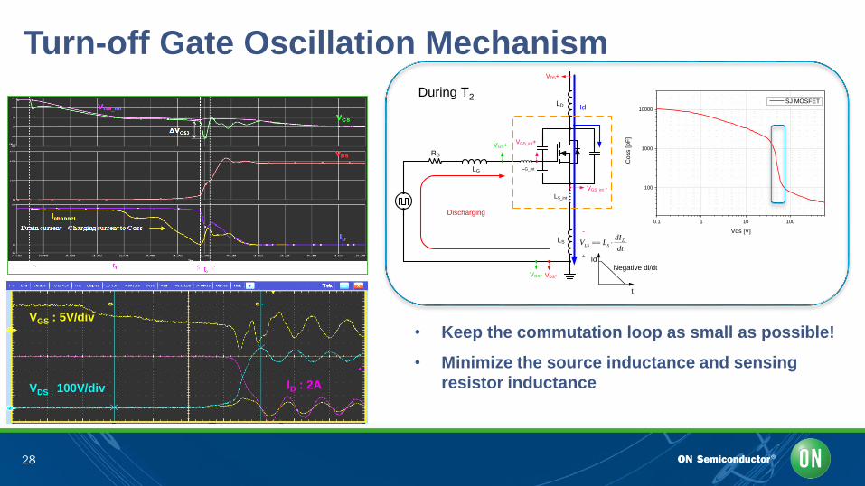
Turn-off Gate Oscillation Mechanism
0.1 1 10 100
100
1000
10000
SJ MOSFET
Co
ss [p
F]
Vds [V]
During T2
RG
LD
LS
LGLG_int
LS_int
dt
dILV D
SLS
+
-
VGS_int -
VGS_int+VGS+
VGS- VDS-
VDS+
Discharging
Id
Id
t
Negative di/dt
VGS : 5V/div
ID : 2AVDS : 100V/div
• Keep the commutation loop as small as possible!
• Minimize the source inductance and sensing
resistor inductance

29
Effects of Source Inductance
LS=1n and 10nH
(a) Vgs waveform for low LS (b) Vgs waveform for High LS
(c) Vds and Id waveform
* Topology : 500W Interleaved CRM PFC
* MOSFET : FCPF13N60N
* Diode : FFPF20UP60DN
* Gate Resistor : Ron=51ohm, Roff=10ohm
Vgs Vgs
Id
Vds

30
Gate oscillation vs Package
Through hole vs SMD vs Kelvin source SMD
ID=8A 600V/199mΩ, Power88 600V/199mΩ, D2PAK 600V/199mΩ, TO220
Kelvin Source SMD SMD Through hole
Turn-off
Transient
Gate Oscillation Gate Oscillation

31
Design Tips - Practical Layout Example
– Boost PFC
Driver and gate resistor far away
from gate pin of MOSFET
Long gate path
Roff
Ron
Increased external
G-D capacitance
G D S G D S
Ron
Don Roff
Driver & Rg as close as
possible to the gate pin of
MOSFET
Connect the driver-stage Gnd
directly to the source pin to
achieve best performance
Qoff
Separate Power GND
and gate driver GND
Bad Layout: Good Layout:

32
Minimized Cgd:
Gate and Drain trace at 90° angle
Minimized source inductance to reference
point for gate drive minimizedTwo independent totem
pole drivers very close to
MOSFET gate
Design Tips - Practical Layout Example
- Paralleling MOSFETs

33
SummaryHow to Use Super-Junction MOSFET in Practical Layouts
• To achieve the best performance of Super-Junction MOSFETs, optimized
layout is required
• Gate driver and Rg must be placed as close as possible to the MOSFET gate pin
• Separate POWER GND and GATE Driver GND
• Minimize parasitic Cgd capacitance and source inductance on PCB
• For paralleling Super-Junction MOSFETs, symmetrical layout is mandatory
• Slow down dv/dt, di/dt by increasing Rg or using ferrite bead

34