dr. lynn fuller - diyhpl.usdiyhpl.us/~nmz787/mems/unorganized/mem_proc.pdfmicroelectronic...
TRANSCRIPT

© September 18, 2012 Dr. Lynn Fuller, Professor
MEMs Process Integration
Page 1
Rochester Institute of Technology
Microelectronic Engineering
ROCHESTER INSTITUTE OF TECHNOLOGYMICROELECTRONIC ENGINEERING
4-9-2008 mem_proc.ppt
Microelectromechanical Systems (MEMs)Process Integration
Dr. Lynn FullerWebpage: http://people.rit.edu/lffeee
Microelectronic EngineeringRochester Institute of Technology
82 Lomb Memorial DriveRochester, NY 14623-5604
Tel (585) 475-2035Fax (585) 475-5041
Email: [email protected] webpage: http://www.microe.rit.edu

© September 18, 2012 Dr. Lynn Fuller, Professor
MEMs Process Integration
Page 2
Rochester Institute of Technology
Microelectronic Engineering
OUTLINE
Surface Micromachine ProcessesSingle Poly Layer Processes
Simple Single Mask ProcessAnchor ProcessAnchor Plus Dimple ProcessSubstrate Isolation Process
Two Poly Layer ProcessesCenter Pin Bearing ProcessFlange Bearing Process
Bulk Micromachine ProcessesSilicon Diaphragm ProcessAdvanced Silicon Diaphragm DesignSurface Diaphragm Design
Integrating Electronics with MEMs

© September 18, 2012 Dr. Lynn Fuller, Professor
MEMs Process Integration
Page 3
Rochester Institute of Technology
Microelectronic Engineering
SIMPLE ONE MASK PROCESS
LPCVD 2.5 µm Poly Silicon
Pattern Poly
2 µm Silicon Dioxide
Etch Oxide Released CantileverAnchor

© September 18, 2012 Dr. Lynn Fuller, Professor
MEMs Process Integration
Page 4
Rochester Institute of Technology
Microelectronic Engineering
ANCHOR PROCESS
2.5 µm Poly Silicon
Pattern Poly
2 µm Silicon Dioxide
Etch OxideReleased Cantilever
Anchor
Pattern Anchor Holes

© September 18, 2012 Dr. Lynn Fuller, Professor
MEMs Process Integration
Page 5
Rochester Institute of Technology
Microelectronic Engineering
ANCHOR PLUS DIMPLE PROCESS
2.5 µm Poly Silicon
Pattern Poly and Etch Oxide
2 µm Silicon Dioxide
Anchor
Pattern Bushing Mold
Bushing
Pattern Anchor Holes

© September 18, 2012 Dr. Lynn Fuller, Professor
MEMs Process Integration
Page 6
Rochester Institute of Technology
Microelectronic Engineering
SUBSTRATE ISOLATION PROCESS
2.5 µm Poly Silicon
Pattern Poly and Etch Oxide
2 µm Silicon Dioxide
Anchor
Pattern Bushing Mold
Bushing
Pattern Anchor Holes
Pad Oxide and Nitride
Pad Oxide and Nitride

© September 18, 2012 Dr. Lynn Fuller, Professor
MEMs Process Integration
Page 7
Rochester Institute of Technology
Microelectronic Engineering
Si
30,000 Å SiO2Si
PhotolithographyEtch in BHF
Si
LPCVD 2.0 µmPoly PhotolithographyEtch Poly in SF6+ O2
Etch SiO2 in BHF
SURFACE MICROMACHINED POLY DIAPHRAGM
Si Si Si

© September 18, 2012 Dr. Lynn Fuller, Professor
MEMs Process Integration
Page 8
Rochester Institute of Technology
Microelectronic Engineering
SURFACE MICROMACHINED POLY DIAPHRAGM
2 µm Poly
1.5 µm Gap
Poly Covered Trench
200 µm
John Castellana, 1997BSµE RIT
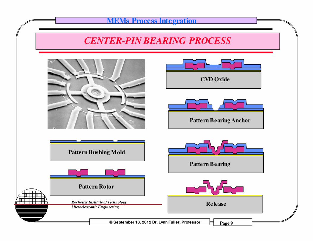
© September 18, 2012 Dr. Lynn Fuller, Professor
MEMs Process Integration
Page 9
Rochester Institute of Technology
Microelectronic Engineering
CENTER-PIN BEARING PROCESS
Pattern Bushing Mold
Pattern Rotor
Pattern Bearing
Release
Pattern Bearing Anchor
CVD Oxide

© September 18, 2012 Dr. Lynn Fuller, Professor
MEMs Process Integration
Page 10
Rochester Institute of Technology
Microelectronic Engineering
CENTER PIN AND SUBSTRATE BEARING PROCESS
Substrate Insulator and 1st Poly
Pattern Bearing
Pattern Substrate Bushing
Pattern Rotor
CVD OxideRelease
Pattern Bearing Anchor

© September 18, 2012 Dr. Lynn Fuller, Professor
MEMs Process Integration
Page 11
Rochester Institute of Technology
Microelectronic Engineering
FLANGE BEARING PROCESS
Pattern Bushing Mold
Bearing Clearance LTO
Bearing Anchor
Bearing Poly Deposition and Etch
Release
Flange Underetch
Pattern Rotor

© September 18, 2012 Dr. Lynn Fuller, Professor
MEMs Process Integration
Page 12
Rochester Institute of Technology
Microelectronic Engineering
BACKSIDE ETCHED BULK MICROMACHINED P+ ETCH STOP DIAPHRAGM PROCESS
1500 Å Si3N4Si
PhotolithographyEtch Nitride inSF6
Si
Boron Doped P+ Etch Stopand n-type Epitaxial Layer
Si
Si
LPCVD Nitride
KOH Wet Etch
P+ Etch Stop
N epi layer 5-10µm
Si
500 µm
P-type Ion Implanted Resistors

© September 18, 2012 Dr. Lynn Fuller, Professor
MEMs Process Integration
Page 13
Rochester Institute of Technology
Microelectronic Engineering
BACKSIDE ETCHED BULK MICROMACHINED POLYSILICON DIAPHRAGM PROCESSES
PhotolithographyEtch Nitride inSF6
Si
10,000 Å Thermal Oxide
LPCVDNitride
KOH Wet EtchStop on Oxide
Si Si
Etch Oxide and Nitride
LPCVD Polysilicon diaphragm of 2 µm thickness and removed from backside of wafer
Si
Si
Si 1500 Å Si3N4Si
Photo define Oxide for diaphragm spacer
Either thin film resistor or capacitive
sensor on poly diaphragm.
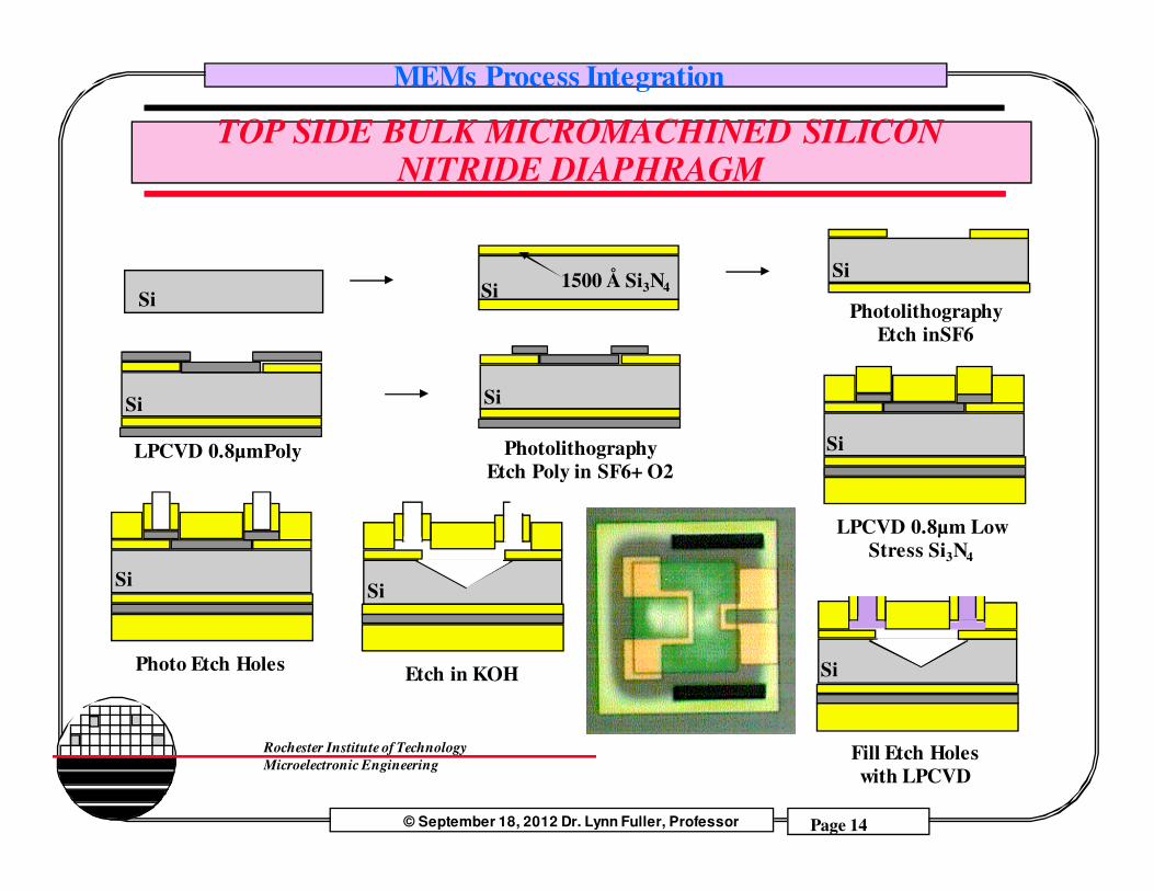
© September 18, 2012 Dr. Lynn Fuller, Professor
MEMs Process Integration
Page 14
Rochester Institute of Technology
Microelectronic Engineering
Si1500 Å Si3N4Si
PhotolithographyEtch inSF6
Si
LPCVD 0.8µmPoly
Si
PhotolithographyEtch Poly in SF6+ O2
Si
LPCVD 0.8µm LowStress Si3N4
Si
Photo Etch Holes
Si
Etch in KOH
Si
Fill Etch Holeswith LPCVD
Si
TOP SIDE BULK MICROMACHINED SILICON NITRIDE DIAPHRAGM

© September 18, 2012 Dr. Lynn Fuller, Professor
MEMs Process Integration
Page 15
Rochester Institute of Technology
Microelectronic Engineering
SCREAM PROCESS
A process that involves anisotropic (Cl2/BCl3) reactive ion etch (RIE) followed by isotropic (SF6) RIE
Single Crystal Reactive Ion Etched Process for Microelectromechanical Structures

© September 18, 2012 Dr. Lynn Fuller, Professor
MEMs Process Integration
Page 16
Rochester Institute of Technology
Microelectronic Engineering
INTEGRATING ELECTRONICS WITH MEMS
Poly Gate PMOS and MEMs at the Same Time
CMOS first MEMs After
MEMs first CMP CMOS After
CMOS and MEMs at the Same Time10x 6 µm
Topology is the main problem

© September 18, 2012 Dr. Lynn Fuller, Professor
MEMs Process Integration
Page 17
Rochester Institute of Technology
Microelectronic Engineering
ELECTRONICS CHIP PLUS MEMS CHIP IN SAME PACKAGE
© September 18, 2012 Dr. Lynn Fuller, Professor
MEMs Process Integration
Page 18
Rochester Institute of Technology
Microelectronic Engineering
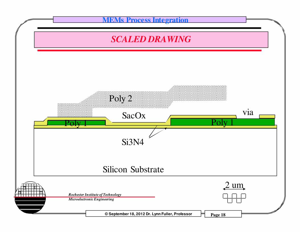
SCALED DRAWING
2 um
Poly 1
Poly 2
SacOx
Silicon Substrate
Si3N4
via
Poly 1

© September 18, 2012 Dr. Lynn Fuller, Professor
MEMs Process Integration
Page 19
Rochester Institute of Technology
Microelectronic Engineering
ADDRESSING TOPOLOGY
1. Use thicker layers for each subsequent layer.
2. Run interconnects in poly over topology because LPCVD
is a conformal deposition process.
3. LOCOS like processes to reduce topology.
4. CMP

© September 18, 2012 Dr. Lynn Fuller, Professor
MEMs Process Integration
Page 20
Rochester Institute of Technology
Microelectronic Engineering
ADDRESSING TOPOLOGY
X and Y movement90° out of phase
X Y
Poly 1 – rotating gear
Poly 2 – anchor pin
Poly 3 - linkage
Where is CMP used and why?
Poly 1 – X/Y motion

© September 18, 2012 Dr. Lynn Fuller, Professor
MEMs Process Integration
Page 21
Rochester Institute of Technology
Microelectronic Engineering
CMOS FIRST MEMS AFTER

© September 18, 2012 Dr. Lynn Fuller, Professor
MEMs Process Integration
Page 22
Rochester Institute of Technology
Microelectronic Engineering
CMOS FIRST MEMS AFTER, TEXAS INSTRUMENTS
TORSIONAL MIRRORS
TI Digital Mirror Array
1 million
Mirrors

© September 18, 2012 Dr. Lynn Fuller, Professor
MEMs Process Integration
Page 23
Rochester Institute of Technology
Microelectronic Engineering
MEMS FIRST CMP THEN CMOS PROCESSING
Buried Polysilicon MEMs with CMP planarization
and CMOS post-fabrication (after Nasby, et al, 1996)

© September 18, 2012 Dr. Lynn Fuller, Professor
MEMs Process Integration
Page 24
Rochester Institute of Technology
Microelectronic Engineering
PROTECTING ELECTRONICS
1. Poly, Aluminum or nitride layer
2. Glass
3. Organics (Protek)
4. One-sided wafer etcher.

© September 18, 2012 Dr. Lynn Fuller, Professor
MEMs Process Integration
Page 25
Rochester Institute of Technology
Microelectronic Engineering
REFERENCES
1. “From Microsensors to Microinstruments,” Petersen, K.E., Sensors and Actuators, vol. A56, nos. 1-2, Aug. 1996, pp. 143-149.2. “The Challenge of Automotive Sensors,” Giachino, J.M., and Miree, T.J., Proceedings of the SPIE Conference on Microlithography and Metrology in Micromachining, Austin, TX, Oct. 23-24, 1995, SPIE Vol. 2640, pp. 89-98.3. “Integrating SCREAM Micromachined Devices with Integrated Circuits,” Shaw, K.A. and Mac Donald, N.C., Proceedings of IEEE International Workshop on Micro Electro Mechanical Systems, San Diego, CA, Fe 11-15, 1996, pp 44-48.4. “Laminated High-Aspect-Ration Microstructures in a Conventional CMOS Process,” Fedder, G.K., et.el., Proceedings of IEEE International Workshop on Micro Electro Mechanical Systems, San Diego, CA, Fe 11-15, 1996, pp 13-18.

© September 18, 2012 Dr. Lynn Fuller, Professor
MEMs Process Integration
Page 26
Rochester Institute of Technology
Microelectronic Engineering
HOMEWORK - PROCESS INTEGRATION
1. List a step by step process to make a cantilever accelerometer
that has a piezoresistive sensor for measuring the acceleration.
There are many different ways to do this so just state your
assumptions and use those for your design.
2. Show a cross section with dimensions.
3. Show a top down layout with dimensions
4. Show example calculations relating acceleration to output
voltage. Again make appropriate assumptions.