Download - Xc instruction manual
XC series PLCUser manual[Instruction]
Spectra Technologies
CatalogCATALOG......................................................................................................................................... 2
1 PROGRAM SUMMARY.............................................................................................................. 8
1-1.PROGRAM CONTROLLER FEATURES.......................................................................................... 91-2.PROGRAM LANGUAGE...............................................................................................................101-2-1.Type...................................................................................................................................101-2-2.Alternation........................................................................................................................ 11
1-3.PROGRAM FORMAT...................................................................................................................11
2 SOFT COMPONENTS FUNCTION.........................................................................................13
2-1.SUMMARY OF THE SOFT COMPONENTS...................................................................................142-2.STRUCTURE OF SOFT COMPONENTS....................................................................................... 172-2-1.Structure of Memory.......................................................................................................172-2-2.Structure of Bit Soft Components.................................................................................19
2-3.SOFT COMPONENTS LIST..........................................................................................................202-3-1.Soft Components List.....................................................................................................202-3-2.Power off Retentive Zone..............................................................................................27
2-4.INPUT/OUTPUT RELAYS (X, Y)..................................................................................................292-5.AUXILIARY RELAY (M)...............................................................................................................312-6.STATUS RELAY (S)....................................................................................................................332-7.TIMER (T).................................................................................................................................. 342-8.COUNTER (C)............................................................................................................................ 362-9.DATA REGISTER (D)...................................................................................................................402-10.CONSTANT...............................................................................................................................422-11.PROGRAM PRINCIPLE...................................................................................................... 43
3 BASIC PROGRAM INSTRUCTIONS..................................................................................... 48
3-1.BASIC INSTRUCTIONS LIST........................................................................................................503-2.[LD] , [LDI] , [OUT]..................................................................................................................523-3.[AND] , [ANI]............................................................................................................................543-4.[OR] , [ORI]..............................................................................................................................553-5.[LDP] , [LDF] , [ANDP] , [ANDF] , [ORP] , [ORF]...............................................................563-6.[LDD] , [LDDI] , [ANDD] , [ANDDI] , [ORD] , [ORDI],[OUTD]........................................573-7.[ORB]........................................................................................................................................583-8.[ANB].........................................................................................................................................593-9.[MCS] , [MCR]......................................................................................................................... 603-10.[ALT]........................................................................................................................................613-11.[PLS] , [PLF].......................................................................................................................... 623-12.[SET] , [RST]......................................................................................................................... 623-13.【OUT】,【RST】FOR THE COUNTERS................................................................................ 643-14. [END]....................................................................................................................................653-15.[GROUP] , [GROUPE].........................................................................................................66
3-16.ITEMS TO NOTE WHEN PROGRAMMING..................................................................................67
4 APPLIED INSTRUCTIONS.......................................................................................................68
4-1.APPLIED INSTRUCTION LIST......................................................................................................694-2.READING METHOD OF APPLIED INSTRUCTIONS.......................................................................744-3.PROGRAM FLOW INSTRUCTIONS..............................................................................................764-3-1.Condition Jump [CJ]....................................................................................................... 774-3-2.Call subroutine [CALL] and Subroutine return [SRET]............................................. 784-3-3.Flow [SET]. [ST]. [STL]. [STLE]....................................................................................794-3-4. [FOR] and [NEXT].........................................................................................................814-3-5. [FEND] and [END].........................................................................................................83
4-4. DATA COMPARE FUNCTION......................................................................................................844-4-1.LD Compare [LD□]........................................................................................................844-4-2.AND Compare [AND□]................................................................................................. 864-4-3.Parallel Compare [OR□]...............................................................................................87
4-5.DATAMOVE................................................................................................................................884-5-1.Data Compare [CMP].....................................................................................................894-5-2.Data zone compare [ZCP].............................................................................................904-5-3.MOV [MOV]......................................................................................................................914-5-4.Data block Move [BMOV].............................................................................................. 934-5-5.Data block Move [PMOV].............................................................................................. 944-5-6.Fill Move [FMOV]............................................................................................................ 954-5-7.FlashROM Write [FWRT]...............................................................................................984-5-8.Zone set [MSET]............................................................................................................. 994-5-9.Zone reset [ZRST]........................................................................................................1004-5-10.Swap the high and low byte [SWAP].......................................................................1014-5-11.Exchange [XCH]..........................................................................................................1024-5-12.Floating move [EMOV]...............................................................................................103
4-6.DATAOPERATION INSTRUCTIONS...........................................................................................1044-6-1 Addition [ADD]..................................................................................................................1044-6-2.Subtraction [SUB]......................................................................................................... 1054-6-3.Multiplication [MUL]......................................................................................................1074-6-4.Division [DIV].................................................................................................................1084-6-5.Increment [INC] & Decrement [DEC].........................................................................1104-6-6.Mean [MEAN].................................................................................................................1114-6-7.Logic AND [WAND], Logic OR [WOR], Logic Exclusive OR [WXOR].................. 1124-6-8.Converse [CML]............................................................................................................ 1144-6-9.Negative [NEG]..............................................................................................................115
4-7.SHIFT INSTRUCTIONS.............................................................................................................. 1164-7-1.Arithmetic shift left [SHL], Arithmetic shift right [SHR].............................................1164-7-2. Logic shift left [LSL], Logic shift right [LSR]................................................................1184-7-3.Rotation shift left [ROL], Rotation shift right [ROR]................................................. 1194-7-4.Bit shift left [SFTL]........................................................................................................ 1204-7-5.Bit shift right [SFTR]..................................................................................................... 1224-7-6.Word shift left [WSFL]..................................................................................................123
4-7-7.Word shift right [WSFR]...............................................................................................1244-8.DATACONVERT....................................................................................................................... 1254-8-1.Single word integer converts to double word integer [WTD]................................. 1264-8-2.16 bits integer converts to float point [FLT]...............................................................1274-8-3.Float point converts to integer [INT]...........................................................................1284-8-4.BCD convert to binary [BIN]........................................................................................1294-8-5.Binary convert to BCD [BCD]......................................................................................1304-8-6.Hex. Converts to ASCII [ASCI]...................................................................................1314-8-7.ASCII converts to hex. [HEX]......................................................................................1324-8-8.Coding [DECO]............................................................................................................. 1334-8-9.High bit coding [ENCO]................................................................................................1354-8-10.Low bit coding [ENCOL]............................................................................................136
4-9.FLOATING OPERATION............................................................................................................1384-9-1.Float Compare [ECMP]................................................................................................1394-9-2.Float Zone Compare [EZCP]...................................................................................... 1404-9-3.Float Add [EADD]..........................................................................................................1414-9-4.Float Sub [ESUB]..........................................................................................................1424-9-5.Float Mul[EMUL]........................................................................................................... 1444-9-6.Float Div [EDIV].............................................................................................................1454-9-7.Float Square Root [ESQR]..........................................................................................1464-9-8.Sine [SIN].......................................................................................................................1474-9-9.Cosine [SIN]...................................................................................................................1484-9-10.TAN [TAN]....................................................................................................................1494-9-11.ASIN [ASIN].................................................................................................................1504-9-12.ACOS [ACOS].............................................................................................................1514-9-13.ATAN [ATAN]............................................................................................................... 152
4-10.RTC INSTRUCTIONS............................................................................................................. 1534-10-1.Read the clock data [TRD]........................................................................................1534-10-2.Write Clock Data [TWR]............................................................................................ 154
5 HIGH SPEED COUNTER (HSC)...........................................................................................156
5-1.FUNCTIONS SUMMARY............................................................................................................1585-2.HSC MODE.............................................................................................................................1585-3.HSC RANGE........................................................................................................................... 1605-4.HSC INPUT WIRING................................................................................................................1605-5.HSC PORTS ASSIGNMENT...................................................................................................... 1615-6.READ/WRITE HSC VALUE.......................................................................................................1665-6-1.Read HSC value [HSCR].............................................................................................1665-6-2.Write HSC value [HSCW]............................................................................................167
5-7.HSC RESET MODE.................................................................................................................1685-8.AB PHASE COUNTER MULTIPLICATION SETTING.................................................................... 1685-9.HSC EXAMPLE........................................................................................................................1695-10. HSC INTERRUPTION...............................................................................................................170
6 PULSE OUTPUT......................................................................................................................178
6-1.FUNCTIONS SUMMARY............................................................................................................1806-2.PULSE OUTPUT TYPES AND INSTRUCTIONS...........................................................................1816-2-1.Unidirectional ration pulse output without ACC/DEC time change [PLSY]..........1816-2-2.Variable Pulse Output [PLSF].....................................................................................1836-2-3.Multi-segment pulse control at relative position [PLSR].........................................1926-2-4.Pulse Segment Switch [PLSNEXT]/ [PLSNT]..........................................................1996-2-5.Pulse Stop [STOP]........................................................................................................2026-2-6.Refresh the pulse number at the port [PLSMV].......................................................2036-2-7.Back to the Origin [ZRN]..............................................................................................2046-2-8.Relative position single-segment pulse control [DRVI]...........................................2106-2-9.Absolute position single-segment pulse control [DRVA]........................................ 2136-2-10.Absolute position multi-segment pulse control [PLSA].........................................2156-2-11.Relative position multi-section pulse control [PTO]...............................................2226-2-12.Absolute position multi-section pulse control [PTOA]...........................................2306-2-13.Pulse Stop [PSTOP]...................................................................................................2346-2-14.Variable frequency single-section pulse [PTF]...................................................... 236
6-3.OUTPUT WIRING..................................................................................................................... 2396-4.NOTES......................................................................................................................................2396-5.SAMPLE PROGRAMS...............................................................................................................2446-6.RELATIVE COILS AND REGISTERS OF PULSE OUTPUT............................................................245
7 COMMUNICATION FUNCTION............................................................................................248
7-1.SUMMARY................................................................................................................................2507-1-1.COM port........................................................................................................................2507-1-2.Communication Parameters............................................................................................3
7-2.MODBUS COMMUNICATION...................................................................................................... 77-2-1.Function..............................................................................................................................77-2-2.Address...............................................................................................................................87-2-3 Modbus communication format.......................................................................................97-2-4.Communication Instructions.......................................................................................... 117-2-5.Application........................................................................................................................20
7-3.FREE FORMAT COMMUNICATION................................................................................... 237-3-1.Communication mode.................................................................................................... 237-3-2.Suitable condition............................................................................................................247-3-3.Instruction form................................................................................................................247-3-4.Free format communication application...................................................................... 28
7-4.CAN BUS FUNCTIONS.............................................................................................................. 307-4-1.Brief Introduction of CAN-bus....................................................................................... 307-4-2.External Wiring................................................................................................................317-4-3.CAN Bus Network Form.................................................................................................317-4-4.CAN-bus Instructions..................................................................................................... 327-4-5.Communication Form of Internal Protocol.................................................................. 367-4-6.CAN Free Format Communication...............................................................................38
8 PID CONTROL FUNCTION......................................................................................................47

8-1.BRIEF INTRODUCTIONS OF THE FUNCTIONS............................................................................488-2.INSTRUCTION FORMS................................................................................................................488-3.PARAMETERS SETTING..............................................................................................................508-3-1.Registers and their functions.........................................................................................518-3-2.Parameters Description................................................................................................. 53
8-4.AUTO TUNE MODE.....................................................................................................................548-5.ADVANCED MODE......................................................................................................................578-6.APPLICATION OUTLINES............................................................................................................578-7.APPLICATION............................................................................................................................. 58
9 C FUNCTION BLOCK...............................................................................................................59
9-1.SUMMARY..................................................................................................................................609-2.INSTRUCTION FORMAT..............................................................................................................609-3.OPERATION STEPS....................................................................................................................619-4.IMPORT AND EXPORT THE FUNCTIONS.................................................................................... 639-5.EDIT THE FUNC BLOCKS...........................................................................................................649-6.PROGRAM EXAMPLE................................................................................................................. 679-7.APPLICATION POINTS................................................................................................................ 709-8.FUNCTION TABLE.......................................................................................................................72
10 SEQUENCE BLOCK...............................................................................................................74
10-1.CONCEPT OF THE BLOCK.....................................................................................................7610-1-1.BLOCK summarization................................................................................................ 7610-1-2.The reason to use BLOCK..........................................................................................77
10-2.CALL THE BLOCK.................................................................................................................. 7810-2-1.Add the BLOCK.............................................................................................................7810-2-2.Move the BLOCK..........................................................................................................8110-2-3.Delete the BLOCK........................................................................................................8310-2-4.Modify the BLOCK........................................................................................................83
10-3.EDIT THE INSTRUCTION INSIDE THE BLOCK.........................................................................8510-3-1.Common item................................................................................................................8510-3-2.Pulse item...................................................................................................................... 8610-3-3.Modbus item..................................................................................................................8710-3-4.Wait item........................................................................................................................ 8710-3-5.Frequency inverter item...............................................................................................8810-3-6.Free format communication item................................................................................91
10-4.RUNNING FORM OF THE BLOCK...........................................................................................9210-5.BLOCK INSTRUCTION EDITING RULES...................................................................................9510-6.BLOCK RELATED INSTRUCTIONS...........................................................................................9810-6-1.Instruction explanation.................................................................................................9810-6-2.The timing sequence of the instructions................................................................. 100
10-7.BLOCK FLAG BIT AND REGISTER.........................................................................................10410-8.PROGRAM EXAMPLE............................................................................................................. 105
11 SPECIAL FUNCTION INSTRUCTIONS............................................................................ 108
11-1.PWM PULSE WIDTH MODULATION......................................................................................11011-2.FREQUENCY TESTING............................................................................................................11111-3.PRECISE TIME........................................................................................................................11311-4.INTERRUPTION........................................................................................................................11611-4-1.External Interruption................................................................................................... 11611-4-2.Time Interruption......................................................................................................... 119
12 APPLICATION PROGRAM SAMPLES.............................................................................122
12-1.PULSE OUTPUTAPPLICATION.............................................................................................. 12312-2.MODBUS COMMUNICATION SAMPLES......................................................................12512-3.FREE FORMAT COMMUNICATION EXAMPLE........................................................................ 128
APPENDIX 1 SPECIAL SOFT DEVICE LIST........................................................................133
APPENDIX 1-1.SPECIALAUXILIARY RELAY LIST...........................................................................134APPENDIX 1-2.LIST OF SPECIAL MEMORY AND SPECIAL DATA REGISTER....................................142APPENDIX 1-3.ID LIST OF THE EXPANSIONS............................................................................... 148APPENDIX 1-4.SPECIAL FLASH REGISTER LIST........................................................................... 153
APPENDIX 2 SPECIAL FUNCTION VERSION REQUIREMENTS................................... 157
APPENDIX 3 APPLIED INSTRUCTION................................................................................. 158
APPENDIX 4 PLC RESOURCE CONFLICT LIST................................................................163
1 Program Summary
1 Program Summary
XC series PLC as the controllers accept the signal and execute the program in thecontroller, to fulfill the requirements from the users. In this chapter, we start with theprogram forms, then introduce the main features, the supported two program languagesetc.
1-1.Programmer Controller Features
1-2.Program Language
1-3.Program Format
1 Program Summary
1-1.Program Controller Features
XC series PLC support two kinds of program languages, instruction list and ladder, thetwo languages can convert to the other;
To avoid the stolen or wrong modifying of user program, we encrypt the program. Whenuploading the encrypted program, it will check in the form of password. This can maintainthe user’s copyright; meantime, it limits the download, to avoid the modification with theprogram spitefully.
When the user program is too long, adding comments to the program and its softcomponents is necessary.
Add offset appendix (like X3[D100]、M10[D100]、D0[D100]) behind coils, data registerscan realize indirect addressing. For example, when D100=9, X3[D100] =X14; M10 [D100]=M19, D0 [D100] =D9
XC series PLC offers enough basic instructions, can fulfill basic sequential control,data moving and comparing, arithmetic operation, logic control, data loop and shiftetc.
XC series PLC also support special compare, high speed pulse, frequency testing,precise time, PID control, position control etc for interruption, high speed counter(HSC).
XC series PLC support C language function block, users can call the edited function blockfreely. This function reduces the program quantity greatly.
XC series PLC support “Stop when power on PLC” function. With this function, when there
Program Language
Security of the Program
Program comments
Rich Basic Functions
C Language Function Block
Stop when power ON Function
Offset Function

1 Program Summary
is a serious problem during PLC running, use this method to stop all output immediately.Besides, with this method, connect PLC when parameters are set wrongly.
XC series PLC support many communication formats, like basic Modbus communication,CABBUS communication, and free format communication. Besides, via special networkmodule, connect to Ether net, GPRS net.
1-2.Program Language
1-2-1.Type
XC series PLC support two types of program language:
Instruction list inputs in the form of “LD”, “AND”, “OUT” etc. This is the basic input form ofthe programs, but it’s hard to read and understand;
E.g.: Step Instruction Soft Components
With sequential control signal and soft components, draw the sequential control graph onprogram interface, this method is called “Ladder”. This method use coil signs etc. torepresent sequential circuit, so it’s easier to understand the program. Meantime, monitorPLC with the circuit’s status.
E.g.:
X0 X2
Y5
Y5
0 LD X0001 OR Y0052 ANI X0023 OUT Y005
Instruction List
Ladder
Communication Function

1 Program Summary
1-2-2.Alternation
Convert the above two methods freely:
1-3.Program Format
The above two program methods can input in the correspond interface separately,especially in the ladder window, there is a instruction hint function, which improves theprogram efficiency greatly;
As in XC series PLC, there are many instructions which have complicate usage and manyusing methods, like pulse output instruction, main unit PID etc. XCPPro also support theconfigure interface for these special instructions. In the correspond configure interface,input the parameters and ID according to the requirements will be ok.
Instructio
n
Ladder
Direct Input
Panel Configuration

1 Program Summary
For the details of panel configuration, please refer XC series PLC user manual【softwarepart】.

2 Soft Component’s Function
2 Soft Components Function
In chapter 1, we briefly tell the program language of XC series PLC. However, the mostimportant element to a program is the operands. These elements relate to the relays andregisters inside the controller. In this chapter, we will describe the functions and usingmethods of these relays and registers.
2-1.Summary of the Soft Components
2-2.Structure of the Soft Components
2-3.List of the Soft Components
2-4.Input/output Relays (X、Y)
2-5.Auxiliary Relays (M)
2-6.Status Relays (S)
2-7.Timers (T)
2-8.Counters (C)
2-9.Data Registers (D)
2-10.Constant (K、H)
2-11.Pointer (P、I)
2-12.Program Principle

2 Soft Component’s Function
2-1.Summary of the Soft Components
There are many relays, timers and counters inside PLC. They all have countless NO(Normally ON) and NC (Normally Closed) contactors. Connect these contactors with thecoils will make a sequential control circuit. Below, we will introduce these soft componentsbriefly;
Usage of the input relays
The input relays are used to accept the external ON/OFF signal, we use X to state.
Address Specify Principle
In each basic unit, specify the ID of input relay, output relay in the form ofX000~X007, X010~X017…,Y000~Y007, Y010~Y017… (octal form)
The expansion module’s ID obeys the principle of channel 1 starts fromX100/Y100, channel 2 starts from X200/Y200… 7 expansions can beconnected in total.
Points to pay attention when using
For the input relay’s input filter, we use digital filter. Users can change the filterparameters via relate settings.
We equip enough output relays inside PLC; for the output relays beyond theinput/output points, use them as auxiliary relays, program as normalcontactors/coils.
Usage of the output relaysOutput relays are the interface of drive external loads, represent with sign Y;
Address Assignment Principle
In each basic unit,assign the ID of output relays in the form of Y000~Y007,Y010~Y017… this octal format.
The ID of expansion obeys the principle of: channel 1 starts from Y100, channel2 starts from Y200… 7 expansions could be connected totally.
Usage of Auxiliary RelaysAuxiliary relays are equipped inside PLC, represent with the sign of M; Address assignment principleIn basic units, assign the auxiliary address in the form of decimal Points to note
This type of relays are different with the input/output relays, they can’t get
Output Relay(Y)
Auxiliary Relays(M)
Input Relay (X)
2 Soft Component’s Function
external load, can only use in program; Retentive relays can keep its ON/OFF status in case of PLC power OFF;
Usage of status relays
Used as relays in Ladder, represent with “S”
Address assignment principle
In basic units, assign the ID in the form of decimal
Points to note
If not used as operation number, they can be used as auxiliary relays, program asnormal contactors/coils. Besides, they can be used as signal alarms, for externaldiagnose.
Usage of the timersTimers are used to calculate the time pulse like 1ms, 10ms, 100ms etc. when reach theset value, the output contactors acts, represent with “T”
Address assignment principle
In basic units, assign the timer’s ID in the form of decimal. But divide ID into several partsaccording to the clock pulse, accumulate or not. Please refer to chapter 2-2 for details. Time pulseThere are three specifications for the timer’s clock pulse: 1ms、10ms、100ms. If choose10ms timer, carry on addition operation with 10ms time pulse; Accumulation/not accumulationThe times are divided into two modes: accumulation time means even the timer coil’sdriver is OFF, the timer will still keep the current value; while the not accumulation timemeans when the count value reaches the set value, the output contact acts, the countvalue clears to be 0;
According to different application and purpose, we can divide the counters to differenttypes as below:
For internal count (for general using/power off retentive usage)
16 bits counter: for increment count, the count range is 1~32,767 32 bits counter: for increment count, the count range is 1~2,147,483,647 These counters can be used by PLC’s internal signal. The response speed is
one scan cycle or longer.
For High Speed Count (Power off retentive)
Status Relays(S)
Timer(T)
Counter(C)
2 Soft Component’s Function
32 bits counter: for increment/decrement count, the count range is-2,147,483,648~ +2,147,483,647
(Single phase increment count, single phase increment/decrement count, AB phasecont) specify to special input points The high speed counter can count 80KHz frequency, it separates with the PLC’s
scan cycle;
Usage of Data Registers
Data Registers are used to store data represent with “D”
Addressing Form
The data registers in XC series PLC are all 16 bits (the highest bit is the sign bit),combine two data registers together can operate 32 bits (the highest bit is the sign bit)data process.
Points to note
Same with other soft components, data registers also have common usage type andpower off retentive type.
Usage of FlashROM registers
FlashROM registers are used to store data soft components, represent with “FD”
Addressing Form
In basic units, FlashROM registers are addressed in form of decimal;
Points to note
Even the battery powered off, this area can keep the data. So this area is used tostore important parameters. FlashROM can write in about 1,000,000 times, and ittakes time at every write. Frequently write can cause permanent damage of FD.
Usage of ED registers
Internal extension registers ED are used to store the data.
Addressing form
In basic units, ED registers are addressed in the form of decimal;
Points to note
Data Register(D)
FlashROM Register(FD)
Internal extension registers(ED)
2 Soft Component’s Function
ED registers are power-loss retentive. It fits for data transfer instructions such asMOV, BMOV, and FMOV.
In every type of data in PLC, B represents Binary, K represents Decimal, and Hrepresents Hexadecimal. They are used to set timers and counters value, oroperands of application instructions.
2-2.Structure of Soft Components
2-2-1.Structure of Memory
In XC series PLC, there are many registers. Besides the common data registers D,FlashROM registers, we can also make registers by combining bit soft components.
Constant(B)(K)(H)
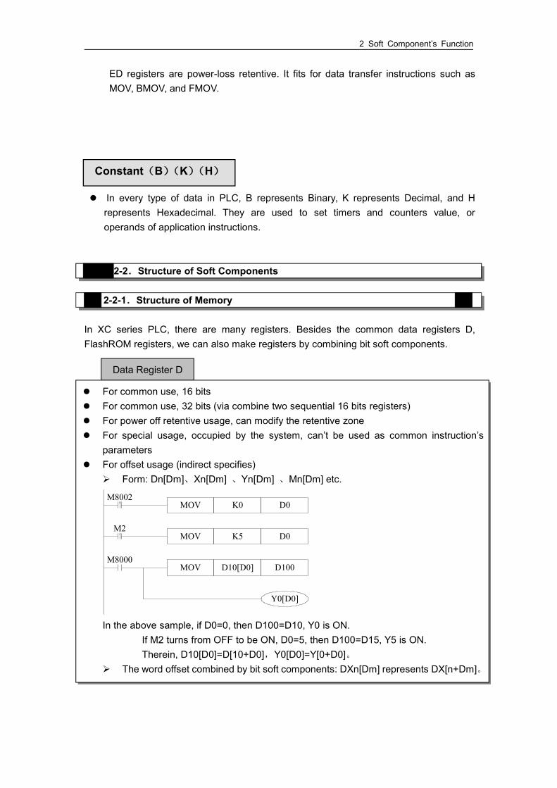
Data Register D
For common use, 16 bits For common use, 32 bits (via combine two sequential 16 bits registers) For power off retentive usage, can modify the retentive zone For special usage, occupied by the system, can’t be used as common instruction’s
parameters For offset usage (indirect specifies)
Form: Dn[Dm]、Xn[Dm] 、Yn[Dm] 、Mn[Dm] etc.
MOV D10[D0] D100M8000
M2
Y0[D0]
MOV K5 D0
M8002MOV K0 D0
In the above sample, if D0=0, then D100=D10, Y0 is ON.If M2 turns from OFF to be ON, D0=5, then D100=D15, Y5 is ON.Therein, D10[D0]=D[10+D0],Y0[D0]=Y[0+D0]。
The word offset combined by bit soft components: DXn[Dm] represents DX[n+Dm]。 The soft components with offset, the offset can be represented by soft component

2 Soft Component’s Function
Expansion internal register
For common usage, 16 bits, For common usage, 32 bits, (via combine two sequential 16 bits
registers)
FlashROM Register FD
For power off retentive usage, 16 bits For power off retentive usage, 16 bits, (via combine two sequential 16 bits
registers) For special usage, occupied by the system, can’t be used as common
Timer T/Counter C
For common usage, 16 bits, represent the current value oftimer/counter;
For common usage, 32 bits, (via combine two sequential 16 bitsregisters)
To represent them, just use the letter + ID method, such as T10, C11.E.g.
MOV D0T11M0
T11Y1
X0T11 K99
In the above example, MOV T11 D0, T11 represents word register;
2 Soft Component’s Function
2-2-2.Structure of Bit Soft Components
Bit soft components structure is simple, the common ones are X、Y、M、S、T、C, besides,a bit of a register can also represents:
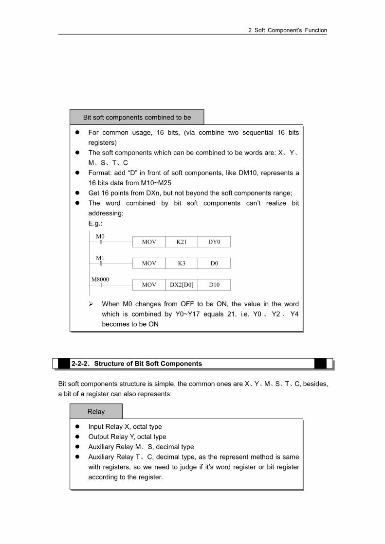
Bit soft components combined to be
For common usage, 16 bits, (via combine two sequential 16 bitsregisters)
The soft components which can be combined to be words are: X、Y、M、S、T、C
Format: add “D” in front of soft components, like DM10, represents a16 bits data from M10~M25
Get 16 points from DXn, but not beyond the soft components range; The word combined by bit soft components can’t realize bit
addressing;E.g.:
MOV K21 DY0M0
MOV K3 D0M1
MOV DX2[D0] D10M8000
When M0 changes from OFF to be ON, the value in the wordwhich is combined by Y0~Y17 equals 21, i.e. Y0 、 Y2 、 Y4becomes to be ON
Relay
Input Relay X, octal type Output Relay Y, octal type Auxiliary Relay M、S, decimal type Auxiliary Relay T、C, decimal type, as the represent method is same
with registers, so we need to judge if it’s word register or bit registeraccording to the register.

2 Soft Component’s Function
2-3.Soft Components List
2-3-1.Soft Components List
Mnemonic NameRange points
10I/O 16 I/O 24 I/O 32 I/O10I/O
16I/O
24 I/O 32 I/O
I/O points※
1
Input Points X0~X4 X0~X7 X0~X13 X0~X17 5 8 12 16OutputPoints
Y0~Y4 Y0~Y7 Y0~Y13 Y0~Y17 5 8 12 16
X※2 InternalRelay
X0~X77 64
Y※3 InternalRelay
Y0~Y77 64
MInternalRelay
M0~M199【M200~M319】※4 320For Special Usage ※5M8000~M8079
128For Special Usage ※5M8120~M8139
Register’s Bit
Composed by register’s bit, support register D Represent method: Dn.m (0≤m≤15): the Nr.m bit of Dn register The represent method of word with offset: Dn[Dm].x Bit of Word can’t compose to be word again;
E.g.:
D0.4Y0
D5[D1].4Y1
D0.4 means when the Nr.4 bit of D0 is 1, set Y0 ON . D5[D1].4 means bit addressing with offset, if D1=5, then D5[D1]
means the Nr.4 bit of D10
XC1 Series
2 Soft Component’s Function
For Special Usage ※5M8170~M8172For Special Usage ※5M8238~M8242For Special Usage ※5M8350~M8370
S Flow S0~S31 32
T Timer
T0~T23: 100ms not accumulation
80
T100~T115: 100ms accumulationT200~T223: 10ms not accumulationT300~T307: 10ms accumulationT400~T403: 1ms not accumulationT500~T503: 1ms accumulation
C Counter
C0~C23: 16 bits forward counter
48
C300~C315: 32 bits forward/backwardcounter
C600~C603: single-phase HSC
C620~C621C630~C631
DData
Register
D0~D99【D100~D149】※4 150
For Special Usage ※5D8000~D8029
138
For Special Usage ※5D8060~D8079For Special Usage ※5D8120~D8179For Special Usage ※5D8240~D8249For Special Usage ※5D8306~D8313For Special Usage ※5D8460~D8469
FDFlashROMRegister※6
FD0~FD411 412For Special Usage ※5FD8000~FD8011
98For Special Usage ※5FD8202~FD8229For Special Usage ※5FD8306~FD8315For Special Usage ※5FD8323~FD8335For Special Usage ※5FD8350~FD8384
Mnemonic
NameRange Points
14 I/O 16 I/O 24/32 I/O 48/60 I/O14I/O
16I/O
24/32I/O
48/60I/O
I/OPoints※1
InputPoints
X0~X7 X0~X7X0~X15X0~X21
X0~X33X0~X43
8 8 14/18 28/36
OutputPoints
Y0~Y5 Y0~Y7Y0~Y11Y0~Y15
Y0~Y23Y0~Y27
6 8 10/14 20/24
XC2 Series
2 Soft Component’s Function
X※2 InternalRelay
X0~X1037 544
Y※3 InternalRelay
Y0~Y1037 544
MInternalRelay
M0~M2999【M3000~M7999】※4 8000
For Special Usage※5M8000~M8767 768
S FlowS0~S511
【S512~S1023】※4 1024
T Timer
T0~T99: 100ms not accumulation
640
T100~T199: 100ms accumulationT200~T299: 10ms not accumulationT300~T399: 10ms accumulationT400~T499: 1ms not accumulationT500~T599: 1ms accumulationT600~T639: 1ms precise time
C Counter
C0~C299: 16 bits forward counter
640
C300~C599: 32 bits forward/backwardcounter
C600~C619: single-phase HSCC620~C629: double-phase HSCC630~C639: AB phase HSC
DData
Register
D0~D999【D4000~D4999】※4 2000
For Special Usage※5D8000~D8511612
For Special Usage※5D8630~D8729
FDFLASHRegister
FD0~FD127 128
For Special Usage※5FD8000~FD8383 384
Mnemonic
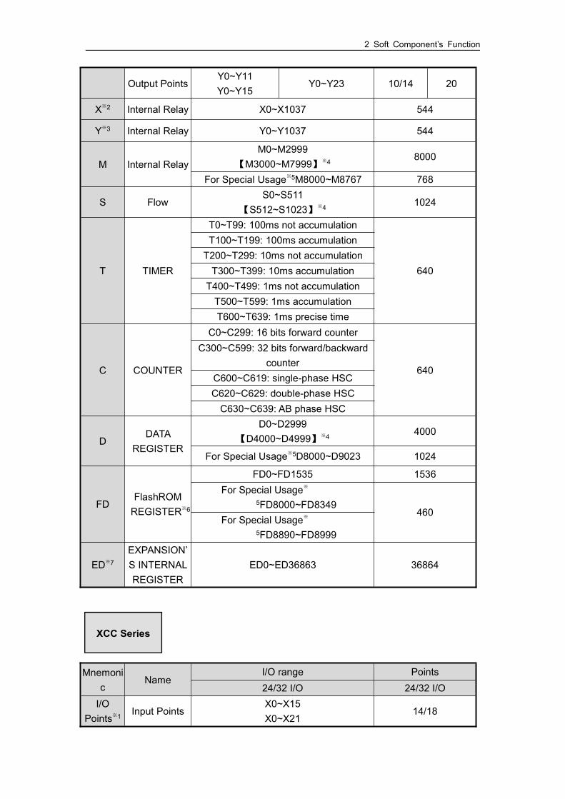
NameRange Points
14 I/O 24/32 I/O 48/60 I/O14I/O
24/32I/O
48/60 I/O
I/OPoints※1
Input Points X0~X7X0~X15X0~X21
X0~X33X0~X43
8 14/1828/36
Output Points Y0~Y5Y0~Y11Y0~Y15
Y0~Y23Y0~Y27
6 10/1420/24
XC3 Series
2 Soft Component’s Function
X※2 Internal Relay X0~X1037 544
Y※3 Internal Relay Y0~Y1037 544
M Internal RelayM0~M2999
【M3000~M7999】※4 8000
For Special Usage※5M8000~M8767 768
S FlowS0~S511
【S512~S1023】※4 1024
T TIMER
T0~T99: 100ms not accumulation
640
T100~T199: 100ms accumulationT200~T299: 10ms not accumulationT300~T399: 10ms accumulation
T400~T499: 1ms not accumulationT500~T599: 1ms accumulationT600~T639: 1ms precise time
C COUNTER
C0~C299: 16 bits forward counter
640C300~C599: 32 bits forward/backward counter
C600~C619: single-phase HSCC620~C629: double-phase HSCC630~C639: AB phase HSC
DDATA
REGISTER
D0~D3999【D4000~D7999】※4 8000
For Special Usage※5D8000~D9023 1024
FDFlashROMREGISTER※
6
FD0~FD3071 3072
For Special Usage※5FD8000~FD9023 1024
ED※7
EXPANSION’S INTERNALREGISTER
ED0~ED16383 16384
Mnemonic
NameI/O RANGE POINTS
24/32 I/O 48/60 I/O 24/32 I/O 48/60 I/O
I/OPoints※1 Input Points
X0~X15X0~X21
X0~X33X0~X43
14/18 28/36
XC5 Series
2 Soft Component’s Function
Output PointsY0~Y11Y0~Y15
Y0~Y23Y0~Y27
10/14 20/24
X※2 Internal Relay X0~X1037 544
Y※3 Internal Relay Y0~Y1037 544
M Internal Relay
M0~M3999【M4000~M7999】※4 8000
For Special Usage※5M8000~M8767 768
S FlowS0~S511
【S512~S1023】※4 1024
T TIMER
T0~T99: 100ms not accumulation
640
T100~T199: 100ms accumulationT200~T299: 10ms not accumulationT300~T399: 10ms accumulationT400~T499: 1ms not accumulationT500~T599: 1ms accumulationT600~T639: 1ms precise time
C COUNTER
C0~C299: 16 bits forward counter
640
C300~C599: 32 bits forward/backwardcounter
C600~C619: single-phase HSCC620~C629: double-phase HSCC630~C639: AB phase HSC
DDATA
REGISTER
D0~D3999【D4000~D7999】※4 8000
For Special Usage※5D8000~D9023 1024
FDFlashROMREGISTER※
6
FD0~FD7167 7168
For Special Usage※5FD8000~FD9023 1024
ED※7
EXPANSION’S INTERNALREGISTER
ED0~ED36863 36864
Mnemonic
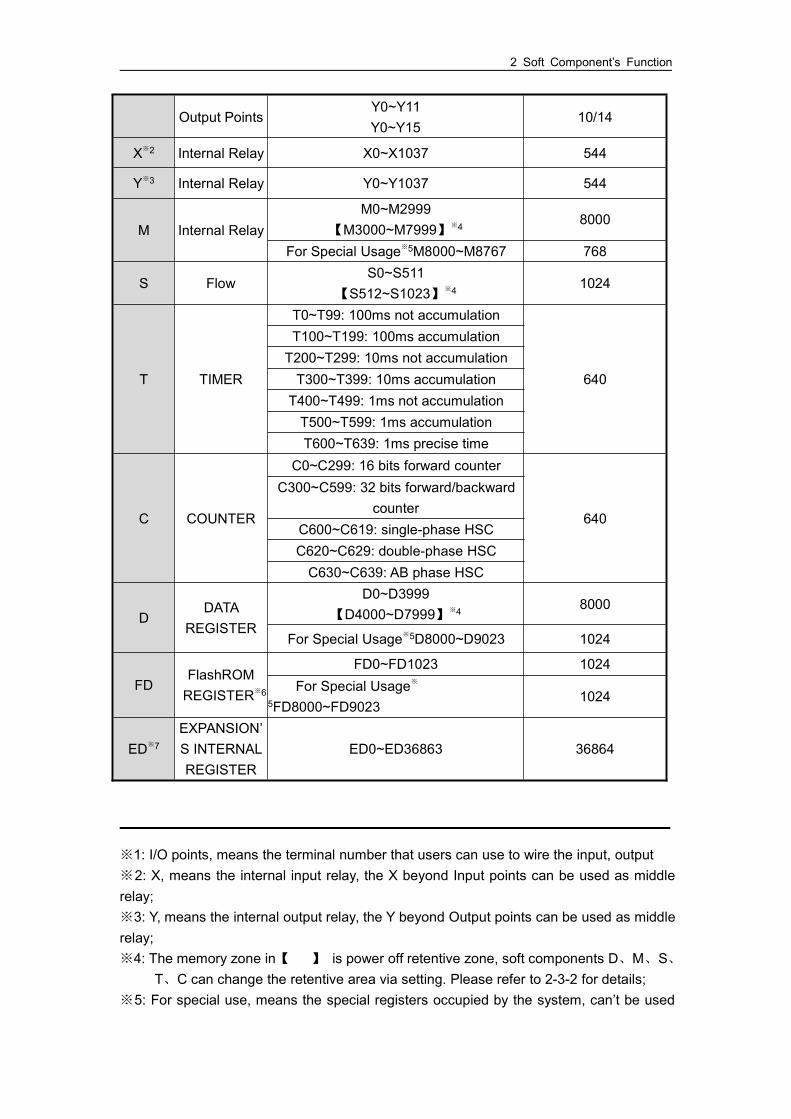
NameI/O range Points
24/32 I/O 48 I/O 24/32 I/O 48 I/OI/O
Points※1 Input PointsX0~X15X0~X21
X0~X33 14/18 28
XCM Series
2 Soft Component’s Function
Output PointsY0~Y11Y0~Y15
Y0~Y23 10/14 20
X※2 Internal Relay X0~X1037 544
Y※3 Internal Relay Y0~Y1037 544
M Internal RelayM0~M2999
【M3000~M7999】※4 8000
For Special Usage※5M8000~M8767 768
S FlowS0~S511
【S512~S1023】※4 1024
T TIMER
T0~T99: 100ms not accumulation
640
T100~T199: 100ms accumulationT200~T299: 10ms not accumulationT300~T399: 10ms accumulation
T400~T499: 1ms not accumulationT500~T599: 1ms accumulationT600~T639: 1ms precise time
C COUNTER
C0~C299: 16 bits forward counter
640
C300~C599: 32 bits forward/backwardcounter
C600~C619: single-phase HSCC620~C629: double-phase HSCC630~C639: AB phase HSC
DDATA
REGISTER
D0~D2999【D4000~D4999】※4 4000
For Special Usage※5D8000~D9023 1024
FDFlashROMREGISTER※6
FD0~FD1535 1536For Special Usage※
5FD8000~FD8349460
For Special Usage※
5FD8890~FD8999
ED※7
EXPANSION’S INTERNALREGISTER
ED0~ED36863 36864
Mnemonic
NameI/O range Points24/32 I/O 24/32 I/O
I/OPoints※1 Input Points
X0~X15X0~X21
14/18
XCC Series
2 Soft Component’s Function
Output PointsY0~Y11Y0~Y15
10/14
X※2 Internal Relay X0~X1037 544
Y※3 Internal Relay Y0~Y1037 544
M Internal RelayM0~M2999
【M3000~M7999】※4 8000
For Special Usage※5M8000~M8767 768
S FlowS0~S511
【S512~S1023】※4 1024
T TIMER
T0~T99: 100ms not accumulation
640
T100~T199: 100ms accumulationT200~T299: 10ms not accumulationT300~T399: 10ms accumulation
T400~T499: 1ms not accumulationT500~T599: 1ms accumulationT600~T639: 1ms precise time
C COUNTER
C0~C299: 16 bits forward counter
640
C300~C599: 32 bits forward/backwardcounter
C600~C619: single-phase HSCC620~C629: double-phase HSCC630~C639: AB phase HSC
DDATA
REGISTER
D0~D3999【D4000~D7999】※4 8000
For Special Usage※5D8000~D9023 1024
FDFlashROMREGISTER※6
FD0~FD1023 1024For Special Usage※
5FD8000~FD90231024
ED※7
EXPANSION’S INTERNALREGISTER
ED0~ED36863 36864
※1: I/O points, means the terminal number that users can use to wire the input, output※2: X, means the internal input relay, the X beyond Input points can be used as middlerelay;※3: Y, means the internal output relay, the Y beyond Output points can be used as middlerelay;※4: The memory zone in【 】 is power off retentive zone, soft components D、M、S、
T、C can change the retentive area via setting. Please refer to 2-3-2 for details;※5: For special use, means the special registers occupied by the system, can’t be used

2 Soft Component’s Function
for other purpose. Please refer to Appendix 1.※6: FlashROM registers needn’t set the power off retentive zone, when power is off (no
battery), the data will not lose※7: Expansion’s internal register ED, require PLC hardware V3.0 or above※8: Input coils、output relays are in octal form, the other registers are in decimal form;※9: The I/O that is not wired with external device can be used as fast internal relays;※10: For the soft components of expansion devices, please refer to relate manuals;
2-3-2.Power off Retentive Zone
The power off retentive area of XC series PLC are set as below, this area can be set byuser again;
Softcomponen
ts
SETAREA
FUNCTION
System’s
defaultvalue
RetentiveZone
XC1Series
DFD820
2Start tag of D power off retentivezone
100 D100~D149
MFD820
3Start tag of M power off retentive
zone200 M200~M319
TFD820
4Start tag of T power off retentive
zone640 Not set
CFD820
5Start tag of C power off retentive
zone320 C320~C631
SFD820
6Start tag of S power off retentive
zone512 S0~S31
XC2Series
DFD820
2Start tag of D power off retentivezone
4000D4000~D499
9
MFD820
3Start tag of M power off retentive
zone3000
M3000~M7999
TFD820
4Start tag of T power off retentive
zone640 Not set
C FD820 Start tag of C power off retentive 320 C320~C639

2 Soft Component’s Function
5 zone
SFD820
6Start tag of S power off retentive
zone512 S512~S1023
XC3Series
DFD820
2Start tag of D power off retentivezone
4000D4000~D799
9
MFD820
3Start tag of M power off retentive
zone3000
M3000~M7999
TFD820
4Start tag of T power off retentive
zone640 Not set
CFD820
5Start tag of C power off retentive
zone320 C320~C639
SFD820
6Start tag of S power off retentive
zone512 S512~S1023
EDFD820
7Start tag of ED power off retentivezone
0ED0~ED1638
3
XC5Series
DFD820
2Start tag of D power off retentivezone
4000D4000~D799
9
MFD820
3Start tag of M power off retentive
zone4000
M4000~M7999
TFD820
4Start tag of T power off retentive
zone640 Not set
CFD820
5Start tag of C power off retentive
zone320 C320~C639
SFD820
6Start tag of S power off retentive
zone512 S512~S1023
EDFD820
7Start tag of ED power off retentive
zone0
ED0~ED36863
XCMSeries
DFD820
2Start tag of D power off retentivezone
4000D4000~D499
9
MFD820
3Start tag of M power off retentive
zone3000
M3000~M7999
TFD820
4Start tag of T power off retentive
zone640 Not set
CFD820
5Start tag of C power off retentive
zone320 C320~C639
SFD820
6Start tag of S power off retentive
zone512 S512~S1023
EDFD820
7Start tag of ED power off retentive
zone0
ED0~ED36863
XCCseries
DFD820
2Start tag of D power off retentivezone
4000D4000~D799
9M FD820 Start tag of M power off retentive 3000 M3000~M799
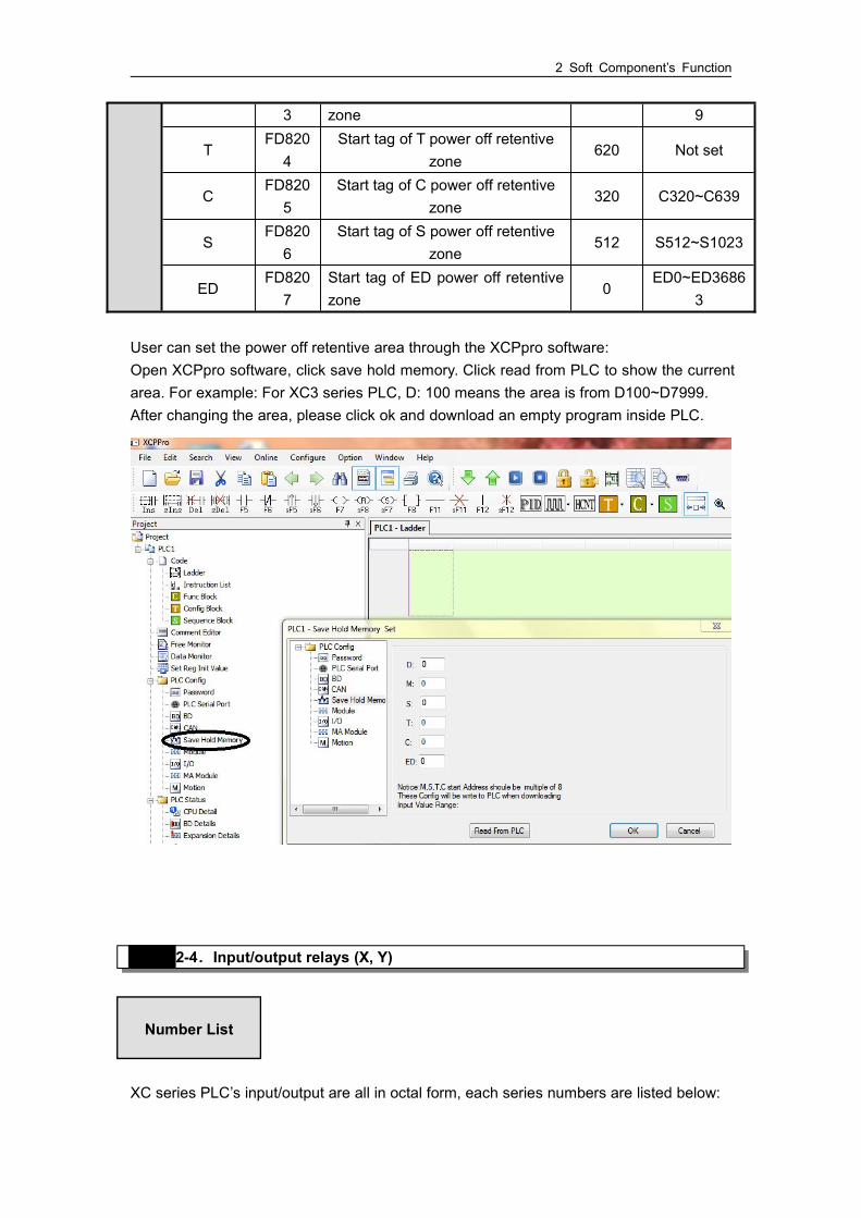
2 Soft Component’s Function
3 zone 9
TFD820
4Start tag of T power off retentive
zone620 Not set
CFD820
5Start tag of C power off retentive
zone320 C320~C639
SFD820
6Start tag of S power off retentive
zone512 S512~S1023
EDFD820
7Start tag of ED power off retentivezone
0ED0~ED3686
3
User can set the power off retentive area through the XCPpro software:Open XCPpro software, click save hold memory. Click read from PLC to show the currentarea. For example: For XC3 series PLC, D: 100 means the area is from D100~D7999.After changing the area, please click ok and download an empty program inside PLC.
2-4.Input/output relays (X, Y)
XC series PLC’s input/output are all in octal form, each series numbers are listed below:
Number List

2 Soft Component’s Function
Series NameRange Points
10I/O 16 I/O 24 I/O 32 I/O 10 I/O16I/O
24 I/O 32 I/O
XC1X X0~X4 X0~X7 X0~X13 X0~X17 5 8 12 16Y Y0~Y4 Y0~Y7 Y0~Y13 Y0~Y17 5 8 12 16
Series NameRange Points
14 I/O 16 I/O 24/32 I/O 48/60 I/O14I/O
16I/O
24/32I/O
48/60I/O
XC2X X0~X7 X0~X7
X0~X15X0~X21
X0~X33X0~X43
8 8 14/18 28/36
Y Y0~Y5 Y0~Y7Y0~Y11Y0~Y15
Y0~Y23Y0~Y27
6 8 10/14 20/24
Series NameRange Points
14 I/O 24/32/42 I/O 48/60 I/O 14 I/O24/32I/O
48/60I/O
XC3
X X0~X7X0~X15X0~X21X0~X27
X0~X33X0~X43
8 14/18 28/36
Y Y0~Y5Y0~Y11Y0~Y15Y0~Y21
Y0~Y23Y0~Y27
6 10/14 20/24
Series NameRange Points
24/32 I/O 48/60 I/O 24/32 I/O 48/60 I/O
XC5X
X0~X15X0~X21
X0~X33X0~X43
14/18 28/36
YY0~Y11Y0~Y15
Y0~Y23Y0~Y27
10/14 20/24
Series NameRange Points
24 I/O 32 I/O 48 I/O 24 I/O 32 I/O 48 I/O
XCMX X0~X15 X0~X21 X0~X33 14 18 28
Y Y0~Y11 Y0~Y15 Y0~Y23 10 14 20
Series Name Range Points

2 Soft Component’s Function
24 I/O 32 I/O 24 I/O 32 I/O
XCCX X0~X15 X0~X21 14 18
Y Y0~Y11 Y0~Y15 10 14
Input Relay X PLC’s input terminals are used to accept the external signal input, while the input
relays are a type of optical relays to connect PLC inside and input terminals; The input relays have countless normally ON/OFF contactors, they can be used
freely; The input relays which are not connected with external devices can be used as fast
internal relays;
Output Relay Y PLC’s output terminals can be used to send signals to external loads. Inside PLC,
output relay’s external output contactors (including relay contactors, transistor’scontactors) connect with output terminals.
The output relays have countless normally ON/OFF contactors, they can be usedfreely;
The output relays which are not connected with external devices can be used as fastinternal relays;
Function
Execution Order
XC series PLCCPU unit
ExternalS
ignalInput
InputTerminalX
OutputTerm
inalY
ExternalS
ignalOutput
XC seriesPLC
CPU unit
ProgramDispose Area
ExternalS
ignalInput
InputTerminalX
InputImage
Area
OutputIm
ageArea
OutputTerm
inalY
ExternalS
ignalOutput

2 Soft Component’s Function
Input Disposal Before PLC executing the program, read every input terminal’s ON/OFF status of
PLC to the image area. In the process of executing the program, even the input changed, the content in
the input image area will not change. However, in the input disposal of next scancycle, read out the change.
Output Disposal Once finish executing all the instructions, transfer the ON/OFF status of output Y
image area to the output lock memory area. This will be the actual output of thePLC.
The contacts used for the PLC’s external output will act according to the device’sresponse delay time.
2-5.Auxiliary Relay (M)
The auxiliary relays M in XC series PLC are all in decimal form; please refer the detailsfrom tables below:
SERIES
NAMERANGE
FOR COMMONUSE
FOR POWER-OFFRETENTIVE USE
FOR SPECIAL USE
XC1 M M000~M199 M200~M319
M8000~M8079M8120~M8139M8170~M8172M8238~M8242M8350~M8370
SERIES
NAMERANGE
FOR COMMONUSE
FOR POWER-OFFRETENTIVE USE
FOR SPECIAL USE
XC2 M M000~M2999 M3000~M7999 M8000~M8767
Number List

2 Soft Component’s Function
SERIES
NAMERANGE
FOR COMMONUSE
FOR POWER-OFFRETENTIVE USE
FOR SPECIAL USE
XC3 M M000~M2999 M3000~M7999 M8000~M8767
SERIES
NAMERANGE
FOR COMMONUSE
FOR POWER-OFFRETENTIVE USE
FOR SPECIAL USE
XC5 M M000~M3999 M4000~M7999 M8000~M8767
SERIES
NAMERANGE
FOR COMMONUSE
FOR POWER-OFFRETENTIVE USE
FOR SPECIAL USE
XCM M M000~M2999 M3000~M7999 M8000~M8767
SERIES
NAMERANGE
FOR COMMONUSE
FOR POWER-OFFRETENTIVE USE
FOR SPECIAL USE
XCC M M000~M2999 M3000~M7999 M8000~M8767
In PLC, auxiliary relays M are used frequently. This type of relay’s coil is same with theoutput relay. They are driven by soft components in PLC;Auxiliary relays M have countless normally ON/OFF contactors. They can be used freely,but this type of contactors can’t drive the external loads. For common use
This type of auxiliary relays can be used only as normal auxiliary relays. I.e. ifpower supply suddenly stops during the running, the relays will disconnect.
Common usage relays can’t be used for power off retentive, but the zone can bemodified;
For Power Off Retentive Use The auxiliary relays for power off retentive usage, even the PLC is OFF, they can
keep the ON/OFF status before power OFF. Power off retentive zone can be modified by the user; Power off retentive relays are usually used to memory the status before stop the
power, then when power the PLC on again, the status can run again;
Function
2 Soft Component’s Function
For Special Usage Special relays refer some relays which are defined with special meanings or
functions, start from M8000. There are two types of usages for special relays, one type is used to drive the
coil, the other type is used to the specified execution;E.g.: M8002 is the initial pulse, activates only at the moment of startM8033 is “all output disabled”
Special auxiliary relays can’t be used as normal relay M;
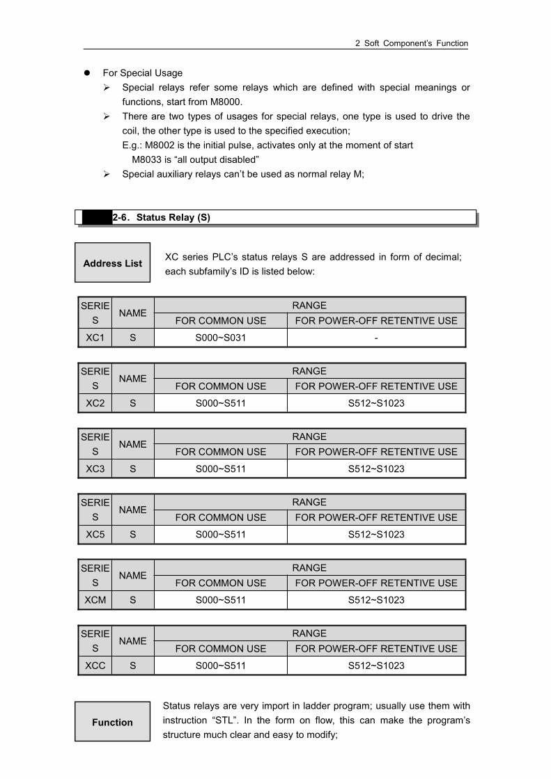
2-6.Status Relay (S)
SERIES
NAMERANGE
FOR COMMON USE FOR POWER-OFF RETENTIVE USE
XC1 S S000~S031 -
SERIES
NAMERANGE
FOR COMMON USE FOR POWER-OFF RETENTIVE USE
XC2 S S000~S511 S512~S1023
SERIES
NAMERANGE
FOR COMMON USE FOR POWER-OFF RETENTIVE USE
XC3 S S000~S511 S512~S1023
SERIES
NAMERANGE
FOR COMMON USE FOR POWER-OFF RETENTIVE USE
XC5 S S000~S511 S512~S1023
SERIES
NAMERANGE
FOR COMMON USE FOR POWER-OFF RETENTIVE USE
XCM S S000~S511 S512~S1023
SERIES
NAMERANGE
FOR COMMON USE FOR POWER-OFF RETENTIVE USE
XCC S S000~S511 S512~S1023
Address List
Function
XC series PLC’s status relays S are addressed in form of decimal;each subfamily’s ID is listed below:
Status relays are very import in ladder program; usually use them withinstruction “STL”. In the form on flow, this can make the program’sstructure much clear and easy to modify;
2 Soft Component’s Function
For common useAfter shut off the PLC power, this type of relays will be OFF status;
For Power Off Retentive Use The status relays for power off retentive usage, even the PLC is OFF, they can
keep the ON/OFF status before power OFF. Power off retentive zone can be modified by the user;
The status relays also have countless “normally ON/OFF” contactors. So users canuse them freely in the program;
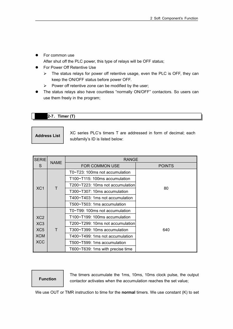
2-7.Timer (T)
SERIES
NAMERANGE
FOR COMMON USE POINTS
XC1 T
T0~T23: 100ms not accumulation
80
T100~T115: 100ms accumulationT200~T223: 10ms not accumulationT300~T307: 10ms accumulationT400~T403: 1ms not accumulationT500~T503: 1ms accumulation
XC2XC3XC5XCMXCC
T
T0~T99: 100ms not accumulation
640
T100~T199: 100ms accumulationT200~T299: 10ms not accumulationT300~T399: 10ms accumulationT400~T499: 1ms not accumulationT500~T599: 1ms accumulationT600~T639: 1ms with precise time
We use OUT or TMR instruction to time for the normal timers. We use constant (K) to set
Address List
Function
XC series PLC’s timers T are addressed in form of decimal; eachsubfamily’s ID is listed below:
The timers accumulate the 1ms, 10ms, 10ms clock pulse, the outputcontactor activates when the accumulation reaches the set value;

2 Soft Component’s Function
the value, or use data register (D) to indirect point the set value;
T10 K100X0
Accum
ulationType
If X001 is ON, then T300 accumulate10ms clock pulse based on thecurrent value; when the accumulationvalue reaches the set value K2000,the timer’s output contact activates.I.e. the output contact activates 2slater.Even if X0 breaks, the timer willcontinue to accumulation onre-starting. The accumulation time is20ms;
Norm
alType
If X0 is ON, then T200 accumulate10ms clock pulse based on thecurrent value; when theaccumulation value reaches the setvalue K200, the timer’s outputcontact activates. I.e. the outputcontact activates 2s later. If X0breaks, the timer resets, the output
T10 is the timer with 100ms as theunit. Specify 100 as the constant,then 0.1s*100=10s timer works;
Write the value of indirectdata register in theprogram or input byvalue switch.If set as the retentiveregister, make sure thebattery voltage isenough, or the value willbe unstable.
《Constant (K)》
《Register (D)》
Specify theset value
Both OUT and TMR can realize thetime function. But if use OUT, thestart time is 0; if use TMR, the starttime is 1 scan cycle

2 Soft Component’s Function
MOV K200 D5
T10 D5
X0
X1
Y0
T2
X0
Y0 X0X0
Y0 T2K200
T2
T1
T2
Y0
X0
T1
T2
X0
Y0T1 T2 T1K10
K20
2-8.Counter (C)
SERIES
NAMERANGE
FOR COMMON USE POINTS
《 output delay OFF
《 twinkle
When X000 is ON, Y000 starts to glitter.T1 controls the OFF time of Y000, T2 controls the ON time of Y000.
When X000 is ON, output Y000;When X000 from ON to OFF, delay T2(20s), then output Y000 is OFF.
Timer T0~T599 is 16 bits linear increment mode (0~K32767), when thetimer’s value reaches the max value K32767, it stops timing. The timer’sstatus keeps still;
Timer Value
ActionExample
Number list XC series PLC counters’ number are all decimal, please see thefollowing table for all the counter numbers.
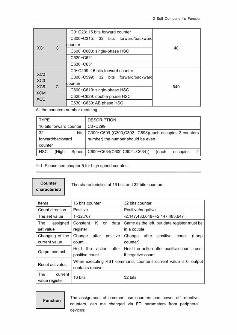
2 Soft Component’s Function
XC1 C
C0~C23: 16 bits forward counter
48
C300~C315: 32 bits forward/backwardcounterC600~C603: single-phase HSCC620~C621C630~C631
XC2XC3XC5XCMXCC
C
C0~C299: 16 bits forward counter
640
C300~C599: 32 bits forward/backwardcounterC600~C619: single-phase HSCC620~C629: double-phase HSCC630~C639: AB phase HSC
All the counters number meaning:
※1: Please see chapter 5 for high speed counter.
Items 16 bits counter 32 bits counterCount direction Positive Positive/negativeThe set value 1~32,767 -2,147,483,648~+2,147,483,647The assignedset value
Constant K or dataregister
Same as the left, but data register must bein a couple
Changing of thecurrent value
Change after positivecount
Change after positive count (Loopcounter)
Output contactHold the action afterpositive count
Hold the action after positive count, resetif negative count
Reset activatesWhen executing RST command, counter’s current value is 0, outputcontacts recover
The currentvalue register
16 bits 32 bits
TYPE DESCRIPTION16 bits forward counter C0~C29932 bitsforward/backwardcounter
C300~C599 (C300,C302...C598)(each occupies 2 countersnumber) the number should be even
HSC (High SpeedCounter)
C600~C634(C600,C602...C634)( (each occupies 2counters number) the number should be even
Countercharacteristi
cs
Function
The characteristics of 16 bits and 32 bits counters:
The assignment of common use counters and power off retentivecounters, can me changed via FD parameters from peripheraldevices;

2 Soft Component’s Function
RST C0X0
C0 K10
Y0
X1
C0
RST C300X3
C300 K10
Y1
X4
C300
M8238X2
16 bits binary increment counters, the valid value is K1~K32,767 (decimaltype constant). The set value K0 and K1 has the same meaning. I.e. theoutput contact works on the first count starts
If cut the PLC power supply, the normalcounter value become zero, theretentive counter can store the value, itcan accumulate the value of last time.
When X001 is ON once, the counter increases 1. When the counter valueis 10, its output is activated. After, when the X001 is ON again, the countercontinues increasing 1.
If X000 is ON, reset counter, the counter value becomes zero. It also can set the counter value in D register. For example, D10=123 is
the same as K123.
32 bits increase/decrease count range is +2147483648 ~ - 2147483647. Setthe increase or decrease count mode in M8238.
If M8238=1, it is decrease mode;M8238=0, it is increase mode.
Set the count value in K or D, if set inD0 register, D0 and D1 will be seemedas one 32bits value.
X004 is ON, C300 starts to count.
16bits
counternorm
al/retentivetype
32bits
counternormal/retentive
type
If X003 is ON, reset the counter and C300 output. If use retentive counter, the count value will be stored in PLC. 32 bits counter can be used as 32 bits register.
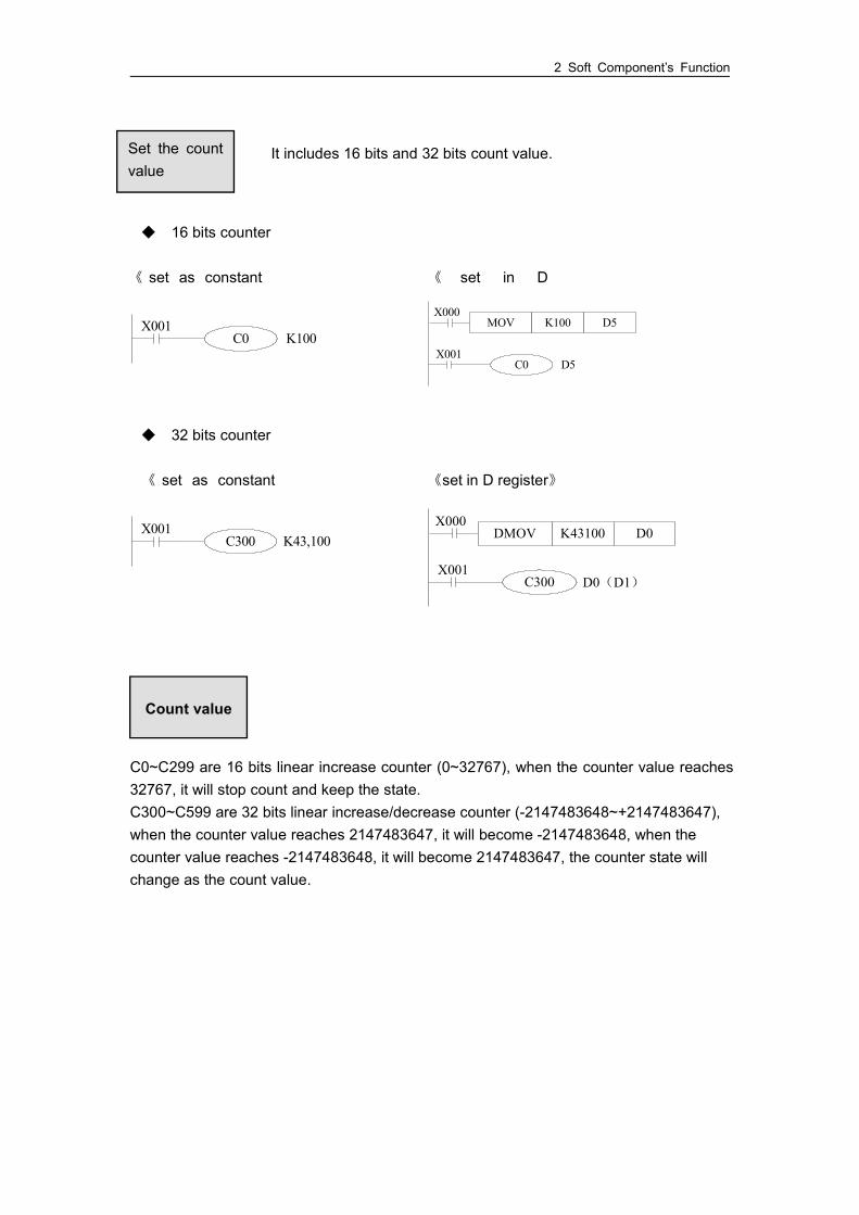
2 Soft Component’s Function
C0X001
K100
C300X001
K43,100
C0~C299 are 16 bits linear increase counter (0~32767), when the counter value reaches32767, it will stop count and keep the state.C300~C599 are 32 bits linear increase/decrease counter (-2147483648~+2147483647),when the counter value reaches 2147483647, it will become -2147483648, when thecounter value reaches -2147483648, it will become 2147483647, the counter state willchange as the count value.
16 bits counter
《 set as constant 《 set in D
32 bits counter
《 set as constant 《set in D register》
Set the countvalue
Count value
MOV K100 D5
C0 D5
X000
X001
DMOV K43100 D0
C300 D0(D1)
X000
X001
It includes 16 bits and 32 bits count value.

2 Soft Component’s Function
2-9.Data register (D)
SERIES
NAMERANGE
FOR COMMONUSE
FOR POWER OFFRETENTIVE USE
FOR SPECIAL USE
XC1 D D0~D99 D100~D149
D8000~D8029
138
D8060~D8079D8120~D8179D8240~D8249D8306~D8313D8460~D8469
XC2 D D0~D999 D4000~D4999D8000~D8511
612D8630~D8729
XC3XC5
D D0~D3999 D4000~D7999 D8000~D9023 1024
XCM D D0~D2999 D3000~D4999 D8000~D9023 1024
Sign bit
B0
D0(16 bits)
0 0 0 0 1 01 00 1 1 0 0 0 0 0b15
0:positive1:negative
Address list
Structure
16bits
16 bits register range is -32,768 ~ +32,767
Use the applied instruction to read and write the register data. Or useother devices such as HMI.
XC series PLC data register D address is shown as below:
Data register is soft element which used to store data, it includes 16bits and 32 bits. ( 32 bits contains two registers, the highest bit is signbit )
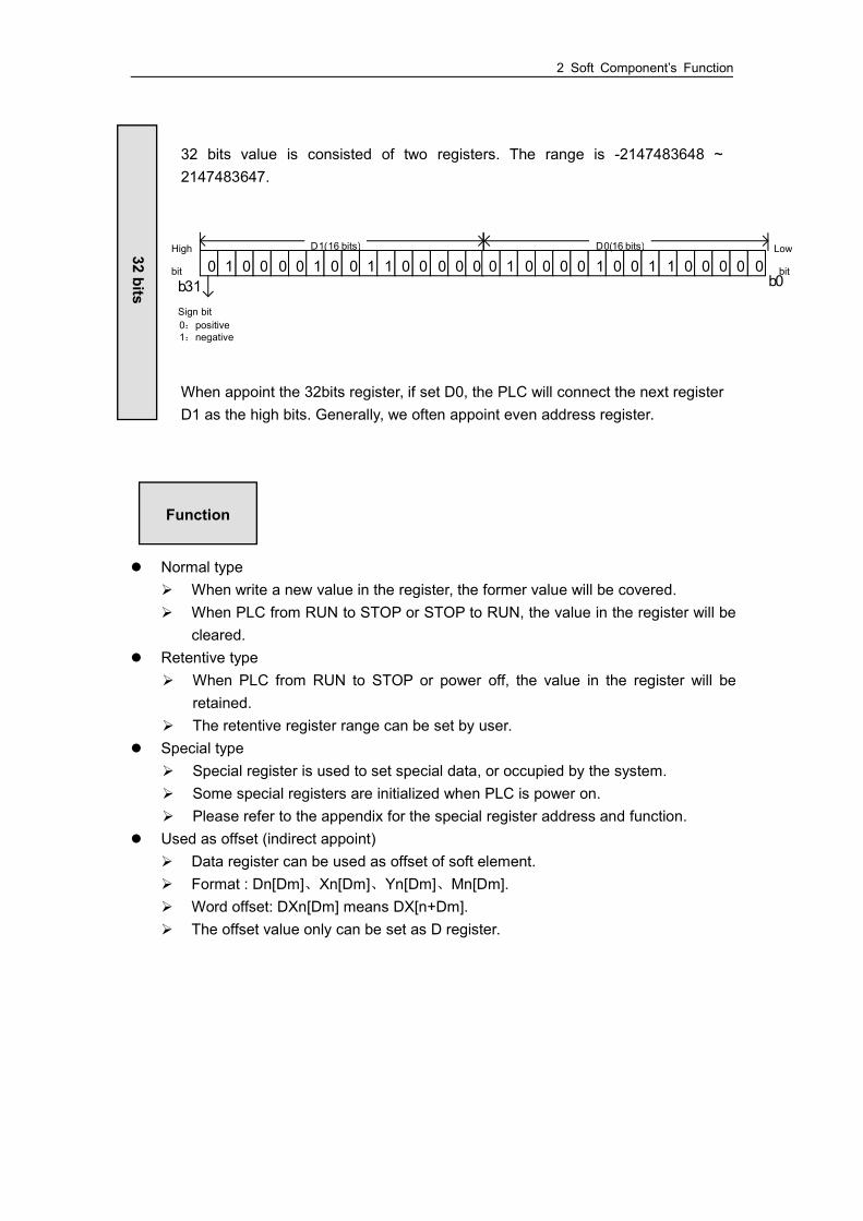
2 Soft Component’s Function
Sign bit
b0
D1(16 bits)
0 0 0 0 1 01 00 1 1 0 0 0 0 0b31
0:positive1:negative
0 0 0 0 1 01 00 1 1 0 0 0 0 0D0(16 bits) Low
bit
High
bit
Normal type When write a new value in the register, the former value will be covered. When PLC from RUN to STOP or STOP to RUN, the value in the register will be
cleared. Retentive type
When PLC from RUN to STOP or power off, the value in the register will beretained.
The retentive register range can be set by user. Special type
Special register is used to set special data, or occupied by the system. Some special registers are initialized when PLC is power on. Please refer to the appendix for the special register address and function.
Used as offset (indirect appoint) Data register can be used as offset of soft element. Format : Dn[Dm]、Xn[Dm]、Yn[Dm]、Mn[Dm]. Word offset: DXn[Dm] means DX[n+Dm]. The offset value only can be set as D register.
32bits
32 bits value is consisted of two registers. The range is -2147483648 ~2147483647.
When appoint the 32bits register, if set D0, the PLC will connect the next registerD1 as the high bits. Generally, we often appoint even address register.
Function

2 Soft Component’s Function
MOV D10[D0] D100M8000
M2
Y0[D0]
MOV K5 D0
M8002MOV K0 D0
When D0=0, D100=D10, Y0 is ON;When M2 is from OFF→ON, D0=5, D100=D15, Y5 is ON.D10[D0]=D[10+D0], Y0[D0]=Y[0+D0].
Data storage
MOV K100 D0M0
M1DMOV K41100 D10
Data transfer
MOV D0 D10M0
Read the timer and counter
MOV C10 D0M0
As the set value of timer and counter
C300 D1
X0
X1
T10 D0
↑
Example
When M0 is ON, write 100 into D0.(16 bits value)
When M1 is ON, write 41100 into D11,D10 (32bits value)
When M0 is ON, transfer the value of D10 to D0
When M0 is ON, move the value of C10 to D0.
When X0 is ON, T10 starts to work, the time is set in D0.
When X1 is ON once, C300 increase 1, when C300value=D1, C300 coil outputs.
Data register D can deal with many kinds of data and realize various controls.
2 Soft Component’s Function
2-10.Constant
DEC: DECIMAL NUMBER The preset number of counter and timer ( constant K) The number of Auxiliary relay M, timer T, counter C, state S. Set as the operand value and action of applied instruction (constant K)
HEX: HEXADECIMAL NUMBER Set as the operand value and action of applied instruction (constant K)
BIN: BINARY NUMBER Inside the PLC, all the numbers will be processed by binary. But when monitoring
on the device, all the binary will be transformed into HEX or DEC.
OCT: OCTAL NUMBER XC series PLC I/O relays are addressed in OCT. Such as [0-7,
10-17,….70-77,100-107].
BCD: BINARY CODE DECIMAL BCD uses 4 bits binary number to display decimal number 0-9. BCD can be used
in 7 segments LED and BCD output digital switch
Other numbers ( float number)XC series PLC can calculate high precision float numbers. It is calculated by
binary numbers, and display by decimal numbers.
Constant KK is used to display decimal numbers. K10 means decimal number 10. It is used to settimer and counter value, operand value of applied instruction.
Constant HH is used to display hex numbers. H10 means hex number 10. It is used to set operandvalue of applied instruction.
Data
Display
XC series PLC use the following 5 number systems.
PLC program should use K, H to process values. K means decimalnumbers, H means hex numbers. Please note the PLC input/outputrelay use octal address.

2 Soft Component’s Function
2-11.PROGRAM PRINCIPLE
Tag P、ITag P、I are used in branch division and interruption.Tag for branch (P) is used in condition jump or subroutine’s jump target;Tag for interruption (I) is used to specify the e input interruption, time interruption;The tags P、I are both in decimal form, each coding principle is listed below:
SERIES NAME RANGEXC1、XC2、XC3、XC5、XCM P P0~P9999
SERIESNAME
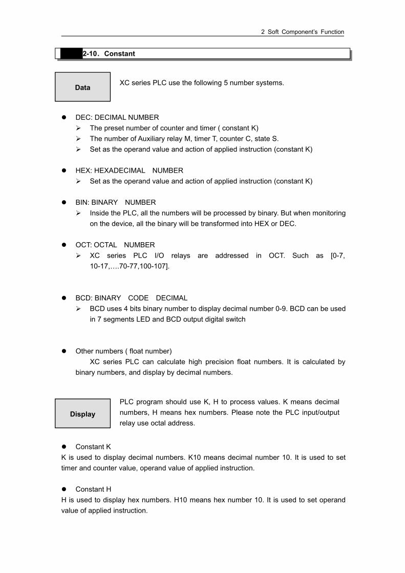
RANGEFOR EXTERNALINTERRUPTION
For time interruptionInput
terminals
Risingedge
interruption
Fallingedge
interruption
XC2 I
X2 I0000 I0001 There are 10 channels timeinterruption, the represented methodis: I40**~I49**. (“**” representsinterruption time, the unit is mm)
X5 I0100 I0101
X10 I0200 I0201
SERIES
NAME I/O
RANGEFOR EXTERNALINTERRUPTION
For time interruptionInputterminal
s
Risingedge
interruption
Fallingedge
interruption
XC3 I
14 X7 I0000 I0001
There are 10 channels timeinterruption, the represented methodis: I40**~I49**. (“**” representsinterruption time, the unit is mm)
2432
X2 I0000 I0001X5 I0100 I0101X10 I0200 I0201
194860
X10 I0000 I0001X7 I0100 I0101X6 I0200 I0201
SERIES
NAME I/ORANGE
FOR EXTERNALINTERRUPTION
For time interruption
2 Soft Component’s Function
Inputterminal
s
Risingedge
interruption
Fallingedge
interruption
XC5 I
2432
X2 I0000 I0001
There are 10 channels timeinterruption, the represented methodis: I40**~I49**. (“**” representsinterruption time, the unit is mm)
X5 I0100 I0101X10 I0200 I0201X11 I0300 I0301X12 I0400 I0401
4860
X2 I0000 I0001X5 I0100 I0101X10 I0200 I0201
SERIES
NAME I/O
RANGEFOR EXTERNALINTERRUPTION
For time interruptionInputterminal
s
Risingedge
interruption
Fallingedge
interruption
XCM I2432
X2 I0000 I0001There are 10 channels timeinterruption, the represented methodis: I40**~I49**. (“**” representsinterruption time, the unit is mm)
X5 I0100 I0101X10 I0200 I0201X11 I0300 I0301X12 I0400 I0401
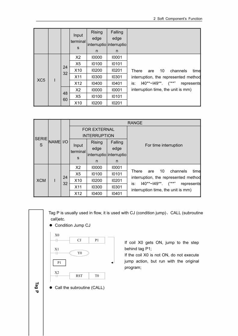
Tag P is usually used in flow, it is used with CJ (condition jump)、CALL (subroutinecall)etc. Condition Jump CJ
X0CJ
X1
X2
P1
T0RST
Y0
P1
Call the subroutine (CALL)
TagP
If coil X0 gets ON, jump to the stepbehind tag P1;If the coil X0 is not ON, do not executejump action, but run with the originalprogram;
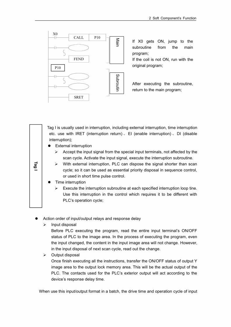
2 Soft Component’s Function
CALLX0
FEND
SRET
P10
P10
Tag I is usually used in interruption, including external interruption, time interruptionetc. use with IRET (interruption return)、 EI (enable interruption)、DI (disableinterruption); External interruption
Accept the input signal from the special input terminals, not affected by thescan cycle. Activate the input signal, execute the interruption subroutine.
With external interruption, PLC can dispose the signal shorter than scancycle; so it can be used as essential priority disposal in sequence control,or used in short time pulse control.
Time interruption Execute the interruption subroutine at each specified interruption loop tine.
Use this interruption in the control which requires it to be different withPLC’s operation cycle;
Action order of input/output relays and response delay Input disposal
Before PLC executing the program, read the entire input terminal’s ON/OFFstatus of PLC to the image area. In the process of executing the program, eventhe input changed, the content in the input image area will not change. However,in the input disposal of next scan cycle, read out the change.
Output disposalOnce finish executing all the instructions, transfer the ON/OFF status of output Yimage area to the output lock memory area. This will be the actual output of thePLC. The contacts used for the PLC’s exterior output will act according to thedevice’s response delay time.
When use this input/output format in a batch, the drive time and operation cycle of input
If X0 gets ON, jump to thesubroutine from the mainprogram;If the coil is not ON, run with theoriginal program;
After executing the subroutine,return to the main program;
TagI
Main
programSubroutin
e

2 Soft Component’s Function
filter and output device will also appear response delay.
Not accept narrow input pulse signalPLC’s input ON/OFF time should be longer than its loop time. If consider input filter’sresponse delay 10ms, loop time is 10ms,then ON/OFF time needs 20 ms separately. So,up to 1,000/(20+20)=25Hz input pulse can’t be disposed. But, this condition could beimproved when use PLC’s special function and applied instructions.
Dual output(Dual coils)action
Y3
Y4
Y3
X1
Y3
X2
As shown in the left map, pleaseconsider the things of using the samecoil Y003 at many positions:E.g. X001=ON,X002=OFF
At first, X001 is ON, its image area isON, output Y004 is also ON.
But, as input X002 is OFF, the imagearea of Y003 is OFF.
So, the actual output is: Y003=OFF,Y004= ON.
When executing dual output (use dualcoil), the back side act in prior.
3 Basic Program Instructions
In this chapter, we tell the basic instructions and their functions.
3-1.Basic Instructions List
3-2.[LD], [LDI], [OUT]
3-3.[AND], [ANI]
3-4.[OR], [ORI]
3-5.[LDP], [LDF], [ANDP], [ANDF], [ORP], [ORF]
3-6.[LDD], [LDDI]
3-7.[ORB]
3-8.[ANB]
3-9.[MCS], [MCR]
3-10.[ALT]
3-11.[PLS], [PLF]
3-12.[SET], [RST]

3-13.[OUT], [RST] (Aim at counter device)
3-14.[NOP], [END]
3-15.[GROUP], [GROUPE]
3-16.Items to be attended when programming

3-1.Basic Instructions List
All XC1, XC2, XC3, XC5, XCM, XCC series support the below instructions:Mnemoni
cFunction Format and Device Chapter
LD(LoaD)
Initial logical operationcontact type NO(normally open)
X、Y、M、S、T、C、Dn.m、FDn.m
3-2
LDD(LoaDDirectly)
Read the status from thecontact directly
X0
D
X
3-6
LDI(LoaDInverse)
Initial logical operationcontact type NC(normally closed)
X、Y、M、S、T、C、Dn.m、FDn.m
3-2
LDDI Read the normallyclosed contact directly
X0
D
X
3-6
LDP(LoaDPulse)
Initial logicaloperation-Rising edge
pulseX、Y、M、S、T、C、Dn.m、FDn.m
3-5
LDF(LoaDFallingPulse)
Initial logicaloperation-Falling /trailing
edge pulseX、Y、M、S、T、C、Dn.m、FDn.m
3-5
AND(AND)
Serial connection of NO(normally open) contacts
M0
X、Y、M、S、T、C、Dn.m、FDn.m
3-3
ANDD Read the status from thecontact directly
X0
D
X
3-6
ANI(AND
Inverse)
Serial connection of NC(normally closed)
contacts
M0
X、Y、M、S、T、C、Dn.m、FDn.m
3-3
ANDDI Read the normallyclosed contact directly
X0
D
3-6
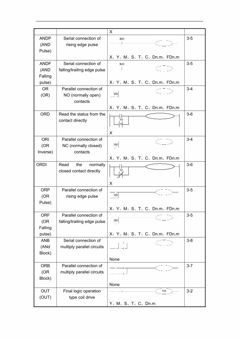
XANDP(ANDPulse)
Serial connection ofrising edge pulse
X、Y、M、S、T、C、Dn.m、FDn.m
3-5
ANDF(ANDFallingpulse)
Serial connection offalling/trailing edge pulse
X、Y、M、S、T、C、Dn.m、FDn.m
3-5
OR(OR)
Parallel connection ofNO (normally open)
contactsX、Y、M、S、T、C、Dn.m、FDn.m
3-4
ORD Read the status from thecontact directly X0
D
X
3-6
ORI(OR
Inverse)
Parallel connection ofNC (normally closed)
contactsX、Y、M、S、T、C、Dn.m、FDn.m
3-4
ORDI Read the normallyclosed contact directly X0
D
X
3-6
ORP(ORPulse)
Parallel connection ofrising edge pulse
X、Y、M、S、T、C、Dn.m、FDn.m
3-5
ORF(ORFallingpulse)
Parallel connection offalling/trailing edge pulse
X、Y、M、S、T、C、Dn.m、FDn.m
3-5
ANB(ANdBlock)
Serial connection ofmultiply parallel circuits
None
3-8
ORB(ORBlock)
Parallel connection ofmultiply parallel circuits
None
3-7
OUT(OUT)
Final logic operationtype coil drive
Y、M、S、T、C、Dn.m
3-2
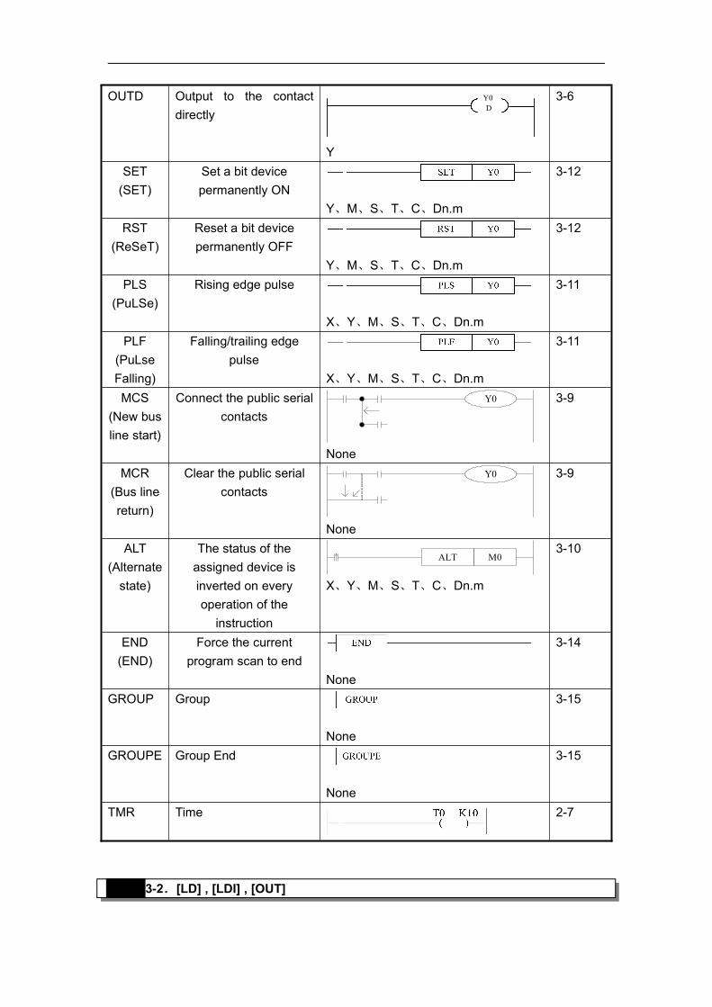
OUTD Output to the contactdirectly
Y0D
Y
3-6
SET(SET)
Set a bit devicepermanently ON
Y、M、S、T、C、Dn.m
3-12
RST(ReSeT)
Reset a bit devicepermanently OFF
Y、M、S、T、C、Dn.m
3-12
PLS(PuLSe)
Rising edge pulse
X、Y、M、S、T、C、Dn.m
3-11
PLF(PuLseFalling)
Falling/trailing edgepulse
X、Y、M、S、T、C、Dn.m
3-11
MCS(New busline start)
Connect the public serialcontacts
Y0
None
3-9
MCR(Bus linereturn)
Clear the public serialcontacts
Y0
None
3-9
ALT(Alternatestate)
The status of theassigned device isinverted on everyoperation of the
instruction
M0ALT
X、Y、M、S、T、C、Dn.m
3-10
END(END)
Force the currentprogram scan to end
None
3-14
GROUP Group
None
3-15
GROUPE Group End
None
3-15
TMR Time 2-7
3-2.[LD] , [LDI] , [OUT]

Mnemonic Function Format and OperandsLD(LoaD)
Initial logic operationcontact type NO(Normally Open)
Operands: X、Y、M、S、T、C、Dn.m、
FDn.mLDI(LoaD Inverse)
Initial logic operationcontact type NC(Normally Closed)
Devices:X、Y、M、S、T、C、Dn.m、
FDn.mOUT(OUT)
Final logic operation typedrive coil
Operands: X、Y、M、S、T、C、Dn.m
Timer, Counter Setting Range of constant K The actual setting value1ms Timer
1~32,7670.001~32.767 sec
10ms Timer 0.01~327.67 sec100ms Timer 0.1~3276.7 sec16 bits counter 1~32,767 Same as the left32 bits counter 1~2,147,483,647 Same as the left
Connect the LD and LDI instructions directly to the left bus bar. Or use them todefine a new block of program when using ANB instruction.
OUT instruction is the coil drive instruction for the output relays、auxiliary relays、status、timers、counters. But this instruction can’t be used for the input relays
Can not sequentially use parallel OUT command for many times. For the timer’s time coil or counter’s count coil, after using OUT instruction, set
constant K is necessary. For the constant K’s setting range、actual timer constant、program’s step relative
to OUT instruction (include the setting value), See table below:
Mnemonic and Function
Statement

Y100
M1203
T 0
X0
Y 1
X1
T0K19
3-3.[AND] , [ANI]
Y2
M2
Y3
X2 M1
X3Y2
T1
Mnemonic Function Format and OperandsAND(AND)
Serial connection ofNO (Normally Open)contacts
M0
Operands: X、Y、M、S、T、C、Dn.m、FDn.mANI(ANdInverse)
Serial connection ofNC (NormallyClosed) contacts
M0
Operands: X、Y、M、S、T、C、Dn.m、FDn.m
LD X0OUT Y100LDI X1OUT M1203OUT T0 K19LD T0OUT Y1
Program
Statements
Use the AND and the ANI instruction for serial connection of contacts. As manycontacts as required can be connected in series. They can be used for manytimes.
The output processing to a coil, through writing the initial OUT instruction is calleda “follow-on” output (For an example see the program below: OUT M2 and OUTY003). Follow-on outputs are permitted repeatedly as long as the output order iscorrect. There’s no limit for the serial connected contacts’ Nr. and follow-on
ProgramLD X2AND M1OUT Y2LD Y2ANI X3OUT M2AND T1OUT Y3
Mnemonic and Function
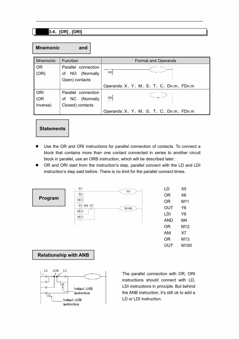
3-4.[OR] , [ORI]
Y6
M100
X5
X6
M11
Y6 M4 X7
M12
M13
Mnemonic Function Format and OperandsOR(OR)
Parallel connectionof NO (NormallyOpen) contacts
Operands: X、Y、M、S、T、C、Dn.m、FDn.mORI(ORInverse)
Parallel connectionof NC (NormallyClosed) contacts
Operands: X、Y、M、S、T、C、Dn.m、FDn.m
Mnemonic andFunction
Statements
Program
The parallel connection with OR, ORIinstructions should connect with LD,LDI instructions in principle. But behindthe ANB instruction, it’s still ok to add aLD or LDI instruction.
LD X5OR X6OR M11OUT Y6LDI Y6AND M4OR M12ANI X7OR M13OUT M100
Use the OR and ORI instructions for parallel connection of contacts. To connect ablock that contains more than one contact connected in series to another circuitblock in parallel, use an ORB instruction, which will be described later;
OR and ORI start from the instruction’s step, parallel connect with the LD and LDIinstruction’s step said before. There is no limit for the parallel connect times.
Relationship with ANB
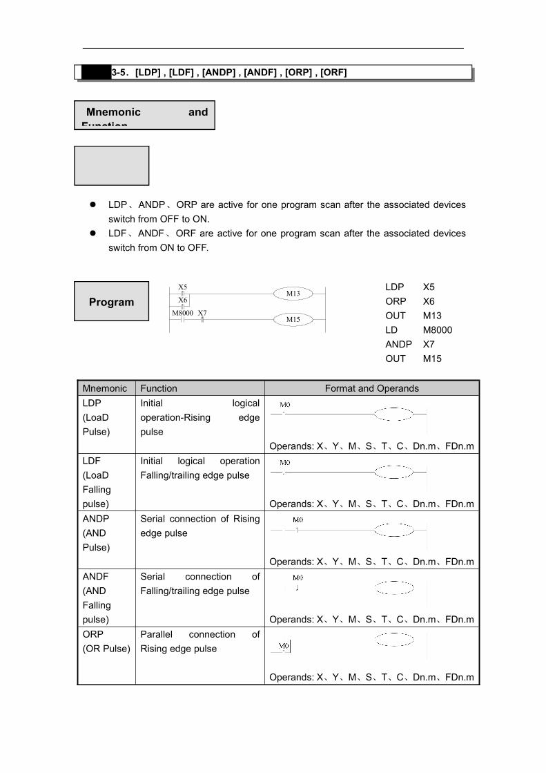
3-5.[LDP] , [LDF] , [ANDP] , [ANDF] , [ORP] , [ORF]
Mnemonic Function Format and OperandsLDP(LoaDPulse)
Initial logicaloperation-Rising edgepulse
Operands: X、Y、M、S、T、C、Dn.m、FDn.mLDF(LoaDFallingpulse)
Initial logical operationFalling/trailing edge pulse
Operands: X、Y、M、S、T、C、Dn.m、FDn.mANDP(ANDPulse)
Serial connection of Risingedge pulse
Operands: X、Y、M、S、T、C、Dn.m、FDn.mANDF(ANDFallingpulse)
Serial connection ofFalling/trailing edge pulse
Operands: X、Y、M、S、T、C、Dn.m、FDn.mORP(OR Pulse)
Parallel connection ofRising edge pulse
Operands: X、Y、M、S、T、C、Dn.m、FDn.m
LDP、ANDP、ORP are active for one program scan after the associated devicesswitch from OFF to ON.
LDF、ANDF、ORF are active for one program scan after the associated devicesswitch from ON to OFF.
M13
M15
X5
X6
M8000 X7
LDP X5ORP X6OUT M13LD M8000ANDP X7OUT M15
Mnemonic andFunction
Program

3-6.[LDD] , [LDDI] , [ANDD] , [ANDDI] , [ORD] , [ORDI],[OUTD]
ORF(ORFallingpulse)
Parallel connection ofFalling/trailing edge pulse
Operands: X、Y、M、S、T、C、Dn.m、FDn.m
Mnemonic Function Format and OperandsLDD Read the status from
the contact directlyX0
D
Devices: XLDDI Read the normally
closed contact directlyX0
D
Devices: XANDD Read the status from
the contact directlyX0
D
Devices: XANDDI Read the normally
closed contact directlyX0
D
Devices: XORD Read the status from
the contact directly X0
D
Devices: XORDI Read the normally
closed contact directly X0
D
Devices: XOUTD Output to the contact
directlyY0D
Devices: Y
Mnemonic and

The function of LDD、ANDD、ORD instructions are similar with LD、AND、OR; LDDI、ANDDI、ORDI instructions are similar with LDI、ANDI、ORI; but if the operand is X, theLDD、ANDD、ORD commands read the signal from the terminals directly, this is theonly difference.
OUTD and OUT are output instructions. But if use OUTD, output immediately if thecondition comes true, needn't wait the next scan cycle.
M13X0
X1
X2D
D
DY0D
3-7.[ORB]
Mnemonic Function Format and DevicesORB(OR Block)
Parallelconnection ofmultiply parallelcircuits
Devices: none
The serial connection with two or more contacts is called "serial block". If parallelconnect the serial block, use LD, LDI at the branch start place, use ORB at the stopplace;
As the ANB instruction,an ORB instruction is an independent instruction and is notassociated with any device number.
There are no limitations to the number of parallel circuits when using an ORB
LDD X0LDDI X2ORD X2ANBOUTD Y0
Program
Statemen
Mnemonic and
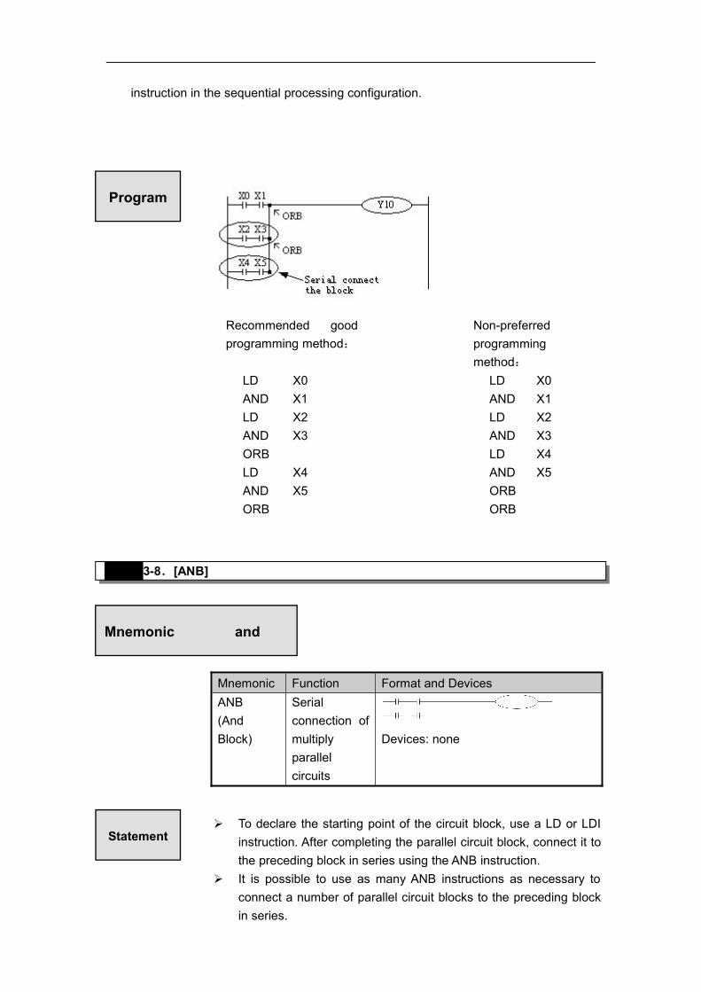
instruction in the sequential processing configuration.
3-8.[ANB]
Mnemonic Function Format and DevicesANB(AndBlock)
Serialconnection ofmultiplyparallelcircuits
Devices: none
Recommended goodprogramming method:
LD X0AND X1LD X2AND X3ORBLD X4AND X5ORBOUT Y10
Non-preferredprogrammingmethod:
LD X0AND X1LD X2AND X3LD X4AND X5ORBORBOUT Y10
Program
To declare the starting point of the circuit block, use a LD or LDIinstruction. After completing the parallel circuit block, connect it tothe preceding block in series using the ANB instruction.
It is possible to use as many ANB instructions as necessary toconnect a number of parallel circuit blocks to the preceding blockin series.
Statement
Mnemonic and
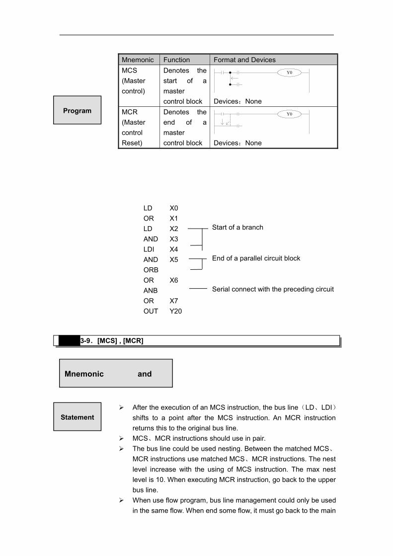
Start of a branch
End of a parallel circuit block
Serial connect with the preceding circuit
3-9.[MCS] , [MCR]
Mnemonic Function Format and DevicesMCS(Mastercontrol)
Denotes thestart of amastercontrol block
Y0
Devices:NoneMCR(MastercontrolReset)
Denotes theend of amastercontrol block
Y0
Devices:None
LD X0OR X1LD X2AND X3LDI X4AND X5ORBOR X6ANBOR X7OUT Y20
Program
After the execution of an MCS instruction, the bus line(LD、LDI)shifts to a point after the MCS instruction. An MCR instructionreturns this to the original bus line.
MCS、MCR instructions should use in pair. The bus line could be used nesting. Between the matched MCS、
MCR instructions use matched MCS、MCR instructions. The nestlevel increase with the using of MCS instruction. The max nestlevel is 10. When executing MCR instruction, go back to the upperbus line.
When use flow program, bus line management could only be usedin the same flow. When end some flow, it must go back to the mainbus line.
Statement
Mnemonic and
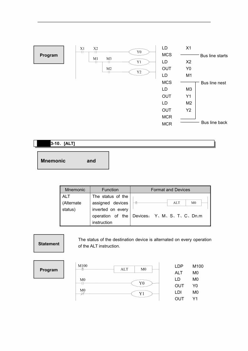
X1 X2
M2
M3M1
Y0
Y1
Y2
3-10.[ALT]
Mnemonic Function Format and DevicesALT(Alternatestatus)
The status of theassigned devicesinverted on everyoperation of theinstruction
M0ALT
Devices: Y、M、S、T、C、Dn.m
M0ALT
M0Y0
M100
Y1M0
LD X1MCSLD X2OUT Y0LD M1MCSLD M3OUT Y1LD M2OUT Y2MCRMCR
Bus line starts
Bus line nest
Bus line back
Program
The status of the destination device is alternated on every operationof the ALT instruction.
LDP M100ALT M0LD M0OUT Y0LDI M0OUT Y1
Statement
Program
Mnemonic and

3-11.[PLS] , [PLF]
Mnemonic Function Format and DevicesPLS(Pulse)
Rising edgepulse
Devices: Y、M、S、T、C、Dn.mPLF(PulseFalling)
Falling/trailingedge pulse
Devices: Y、M、S、T、C、Dn.m
X0PLS M0
M0SET Y0
X1PLF M1
M1RST Y0
When a PLS instruction is executed, object devices Y and Moperate for one operation cycle after the drive input signal hasturned ON.
When a PLF instruction is executed, object devices Y and Moperate for one operation cycle after the drive input signal has
LD X0PLS M0LD M0SET Y0
----------------------LD X1PLF M1LD M1RST Y0
Statement
Program
Mnemonic and
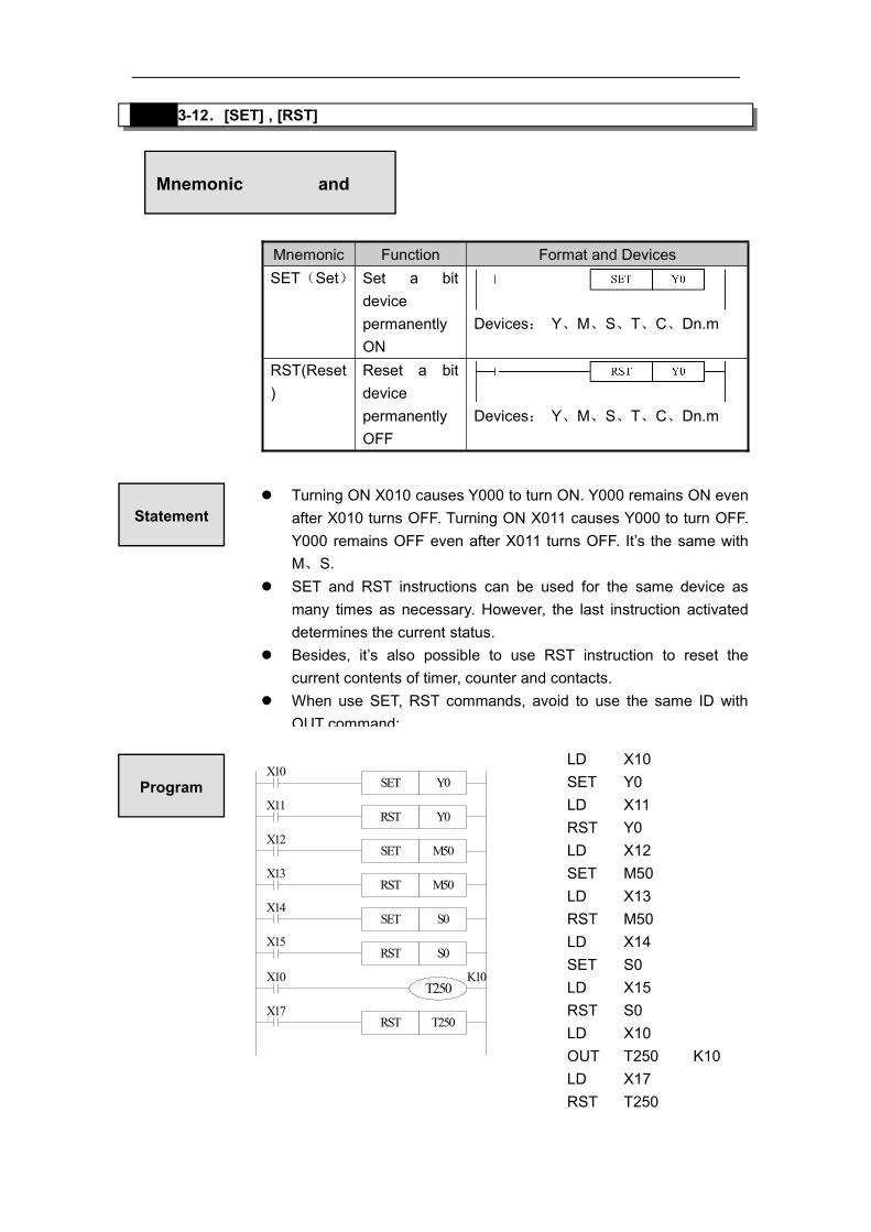
3-12.[SET] , [RST]
Mnemonic Function Format and DevicesSET(Set) Set a bit
devicepermanentlyON
Devices: Y、M、S、T、C、Dn.m
RST(Reset)
Reset a bitdevicepermanentlyOFF
Devices: Y、M、S、T、C、Dn.m
X10SET Y0
X11RST Y0
X12SET M50
X13RST M50
X14SET S0
X15RST S0
X10T250
K10
X17RST T250
Turning ON X010 causes Y000 to turn ON. Y000 remains ON evenafter X010 turns OFF. Turning ON X011 causes Y000 to turn OFF.Y000 remains OFF even after X011 turns OFF. It’s the same withM、S.
SET and RST instructions can be used for the same device asmany times as necessary. However, the last instruction activateddetermines the current status.
Besides, it’s also possible to use RST instruction to reset thecurrent contents of timer, counter and contacts.
When use SET, RST commands, avoid to use the same ID withOUT command;
LD X10SET Y0LD X11RST Y0LD X12SET M50LD X13RST M50LD X14SET S0LD X15RST S0LD X10OUT T250 K10LD X17RST T250
Statement
Program
Mnemonic and

3-13.【OUT】,【RST】for the counters
Mnemonic Function Format and DevicesOUT Final logic
operationtype coil drive Device:K、D
RST Reset a bitdevicepermanentlyOFF
Device:C
C0 carries on increase count forthe OFF→ON of X011. When reachthe set value K10, output contactC0 activates. Afterwards, evenX011 turns from OFF to ON,counter’s current value will notchange, output contact keep onactivating.To clear this, let X010 be theactivate status and reset the outputcontact. It’s necessary to assignconstant K or indirect dataregister’s ID behind OUT
Programming of
interior counter
Mnemonic and
Counter used for power cut retentive.Even when power is cut, hold thecurrentvalue and output contact’s actionstatus

3-14. [END]
Mnemonic Function Format and Devices:NoneEND(END)
Force thecurrentprogram scanto end
Devices: None
In the preceding example, when M0 is ON, carry on positive count with OFF→ON of X0.
Counter’s current value increase, when reach the set value (K or D), theoutput contact is reset.
When M1 is ON, counter’s C600 output contact is reset, counter’s currentvalue turns to be 0.
Programming of highspeed
PLC repeatedly carry on input disposal,program executing and output disposal. Ifwrite END instruction at the end of theprogram, then the instructions behind ENDinstruction won’t be executed. If there’s noEND instruction in the program, the PLCexecutes the end step and then repeatexecuting the program from step 0.When debug, insert END in each programsegment to check out each program’s action.Then, after confirm the correction of precedingblock’s action, delete END instruction.Besides, the first execution of RUN beginswith END instruction.
Statement
Mnemonic and
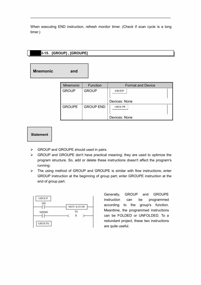
When executing END instruction, refresh monitor timer. (Check if scan cycle is a longtimer.)
3-15.[GROUP] , [GROUPE]
Mnemonic Function Format and DeviceGROUP GROUP
Devices: NoneGROUPE GROUP END
Devices: None
GROUP and GROUPE should used in pairs. GROUP and GROUPE don't have practical meaning; they are used to optimize the
program structure. So, add or delete these instructions doesn't affect the program'srunning;
The using method of GROUP and GROUPE is similar with flow instructions; enterGROUP instruction at the beginning of group part; enter GROUPE instruction at theend of group part.
Generally, GROUP and GROUPEinstruction can be programmedaccording to the group's function.Meantime, the programmed instructionscan be FOLDED or UNFOLDED. To aredundant project, these two instructionsare quite useful.
Statement
Mnemonic and

3-16.Items to Note When Programming
1、Contacts’ structure and step numberEven in the sequential control circuit with the same action, it’s also available to simple theprogram and save program’s steps according to the contacts’ structure.General program principle is:
(a) Write the circuit with many serial contacts on the top;(b) Write the circuit with many parallel contacts in the left.
2、Program’s executing sequenceHandle the sequential control program by【From top to bottom】and【From left to right】Sequential control instructions also encode following this flow.
3、Dual output dual coil’s activation and the solution If carry on coil’s dual output (dual coil) in the sequential control program, then the
backward action is prior. Dual output (dual coil) doesn’t go against the input rule at the program side. But as
the preceding action is very complicate, please modify the program as in the followingexample.
Y0
Y0
X0 X2
X3 X4
Y0X0 X2
X3 X4
M0
M1
X0 X2
X3 X4
Y0M0
M1
There are other methods. E.g. jump instructions or step ladder. However, when use stepladder, if the main program’s output coil is programmed, then the disposal method is thesame with dual coil, please note this.

4 Applied Instructions
In this chapter, we describe applied instruction’s function of XC series PLC.
4-1.Table of Applied Instructions
4-2.Reading Method of Applied Instructions
4-3.Flow Instructions
4-4.Contactors Compare Instructions
4-5.Move Instructions
4-6.Arithmetic and Logic Operation Instructions
4-7.Loop and Shift Instructions
4-8.Data Convert
4-9.Floating Operation
4-10.Clock Operation

4-1.Applied Instruction List
Mnemonic Function Ladder chart Chapter
Program Flow
CJ Condition jump CJ Pn 4-3-1
CALL Call subroutine CALL Pn 4-3-2
SRET Subroutine return SRET 4-3-2
STL Flow start STL Sn 4-3-3
STLE Flow end STLE 4-3-3
SETOpen the assigned flow,close the current flow
SET Sn 4-3-3
STOpen the assigned flow,not close the current flow
ST Sn 4-3-3
FOR Start a FOR-NEXT loop FOR S 4-3-4
NEXT End of a FOR-NEXT loop NEXT 4-3-4
FEND Main program END FEND 4-3-5
END Program END 4-3-5
Data CompareLD= LD activates if (S1) = (S2)
LD= S1 S2 4-4-1
LD> LD activates if (S1) > (S2)LD> S1 S2 4-4-1
LD< LD activates if (S1) =< (S2)LD< S1 S2 4-4-1
LD<> LD activates if(S1)≠(S2)LD<> S1 S2 4-4-1
LD<= LD activates if(S1)≤(S2)LD<= S1 S2 4-4-1
LD>= LD activates if(S1)≥(S2)LD>= S1 S2 4-4-1

AND= AND activates if(S1)=
(S2)AND= S1 S2 4-4-2
AND> AND activates if(S1)>
(S2)AND> S1 S2 4-4-2
AND< AND activates if(S1)<
(S2)AND< S1 S2 4-4-2
AND<> AND activates if(S1)≠(S2)AND<> S1 S2 4-4-2
AND<= AND activates if(S1)≤(S2)AND<= S1 S2 4-4-2
AND>= AND activates if(S1)≥(S2)AND= S1 S2 4-4-2
OR= OR activates if(S1)=(S2)OR= S1 S2 4-4-3
OR> OR activates if(S1)>(S2)OR> S1 S2 4-4-3
OR< OR activates if(S1)<(S2)OR< S1 S2 4-4-3
OR<> OR activates if(S1)≠(S2)OR<> S1 S2 4-4-3
OR<= OR activates if(S1)≤(S2)OR<= S1 S2 4-4-3
OR>= OR activates if(S1)≥(S2)OR>= S1 S2 4-4-3
Data Move
CMP Compare the data CMP S1 S D 4-5-1
ZCPCompare the data incertain area
ZCP S1 S2 S D 4-5-2
MOV Move MOV S D 4-5-3
BMOV Block move BMOV S D n 4-5-4
PMOV Transfer the Data block PMOV S D n 4-5-5
FMOV Multi-points repeat move FMOV S D n 4-5-6
FWRT Flash ROM written FWRT S D 4-5-7
MSET Zone set MSET S1 S2 4-5-8
ZRST Zone reset ZRST S1 S2 4-5-9

SWAP Swap the high and low byte 4-5-10
XCH Exchange two values 4-5-11
EMOV Float move 4-5-12
Data Operation
ADD Addition ADD S1 S2 D 4-6-1
SUB Subtraction SUB S1 S2 D 4-6-2
MUL Multiplication 4-6-3
DIV Division 4-6-4
INC Increment 4-6-5
DEC Decrement 4-6-5
MEAN Mean MEAN S D n 4-6-6
WAND Word And WAND S1 S2 D 4-6-7
WOR Word OR WOR S1 S2 D 4-6-7
WXOR Word exclusive OR WXOR S1 S2 D 4-6-7
CML Compliment CML S D 4-6-8
NEG Negative 4-6-9
Data Shift
SHL Arithmetic Shift Left SHL D n 4-7-1
SHR Arithmetic Shift Right SHR D n 4-7-1
LSL Logic shift left 4-7-2
LSR Logic shift right 4-7-2
ROL Rotation shift left 4-7-3
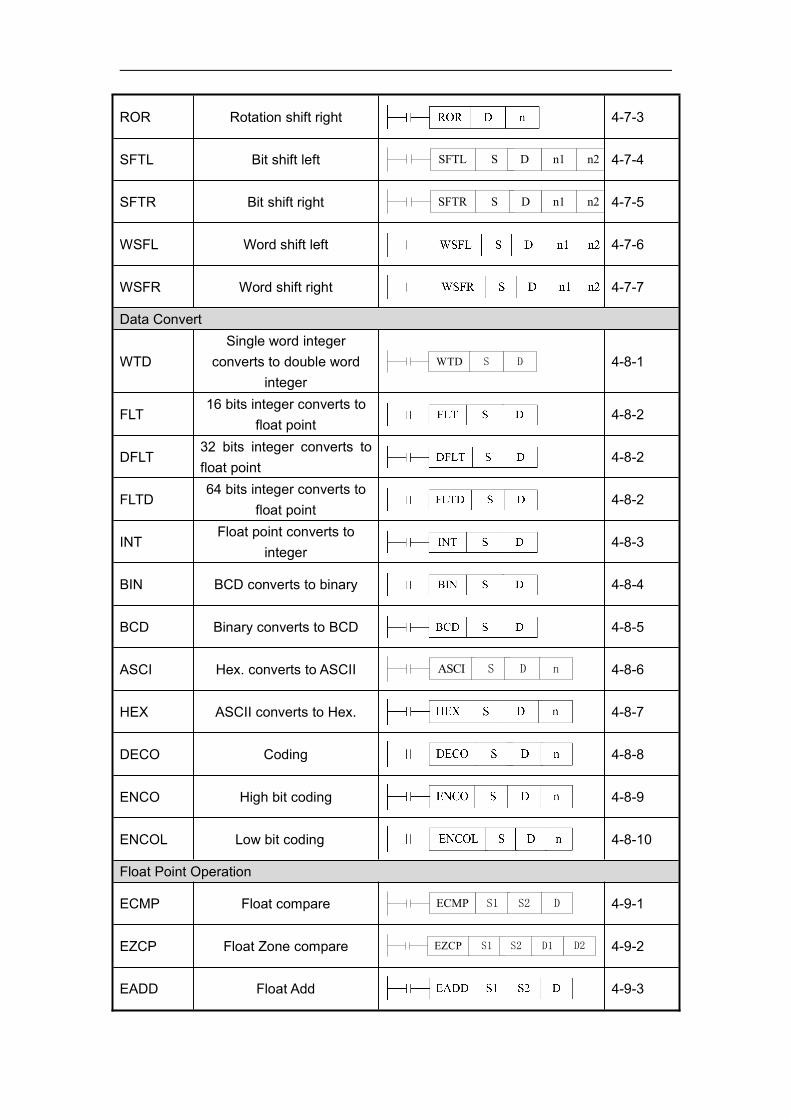
ROR Rotation shift right 4-7-3
SFTL Bit shift left SFTL S D n1 n2 4-7-4
SFTR Bit shift right SFTR S D n1 n2 4-7-5
WSFL Word shift left 4-7-6
WSFR Word shift right 4-7-7
Data Convert
WTDSingle word integer
converts to double wordinteger
WTD S D 4-8-1
FLT16 bits integer converts to
float point4-8-2
DFLT32 bits integer converts tofloat point
4-8-2
FLTD64 bits integer converts to
float point4-8-2
INTFloat point converts to
integer4-8-3
BIN BCD converts to binary 4-8-4
BCD Binary converts to BCD 4-8-5
ASCI Hex. converts to ASCII ASCI S D n 4-8-6
HEX ASCII converts to Hex. 4-8-7
DECO Coding 4-8-8
ENCO High bit coding 4-8-9
ENCOL Low bit coding 4-8-10
Float Point Operation
ECMP Float compare ECMP S1 S2 D 4-9-1
EZCP Float Zone compare EZCP S1 S2 D1 D2 4-9-2
EADD Float Add 4-9-3
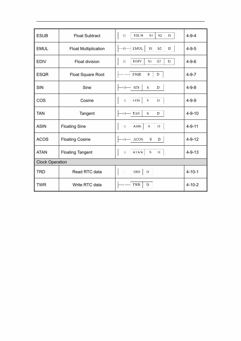
ESUB Float Subtract 4-9-4
EMUL Float Multiplication 4-9-5
EDIV Float division 4-9-6
ESQR Float Square Root 4-9-7
SIN Sine 4-9-8
COS Cosine 4-9-9
TAN Tangent 4-9-10
ASIN Floating Sine 4-9-11
ACOS Floating Cosine 4-9-12
ATAN Floating Tangent 4-9-13
Clock Operation
TRD Read RTC data 4-10-1
TWR Write RTC data 4-10-2
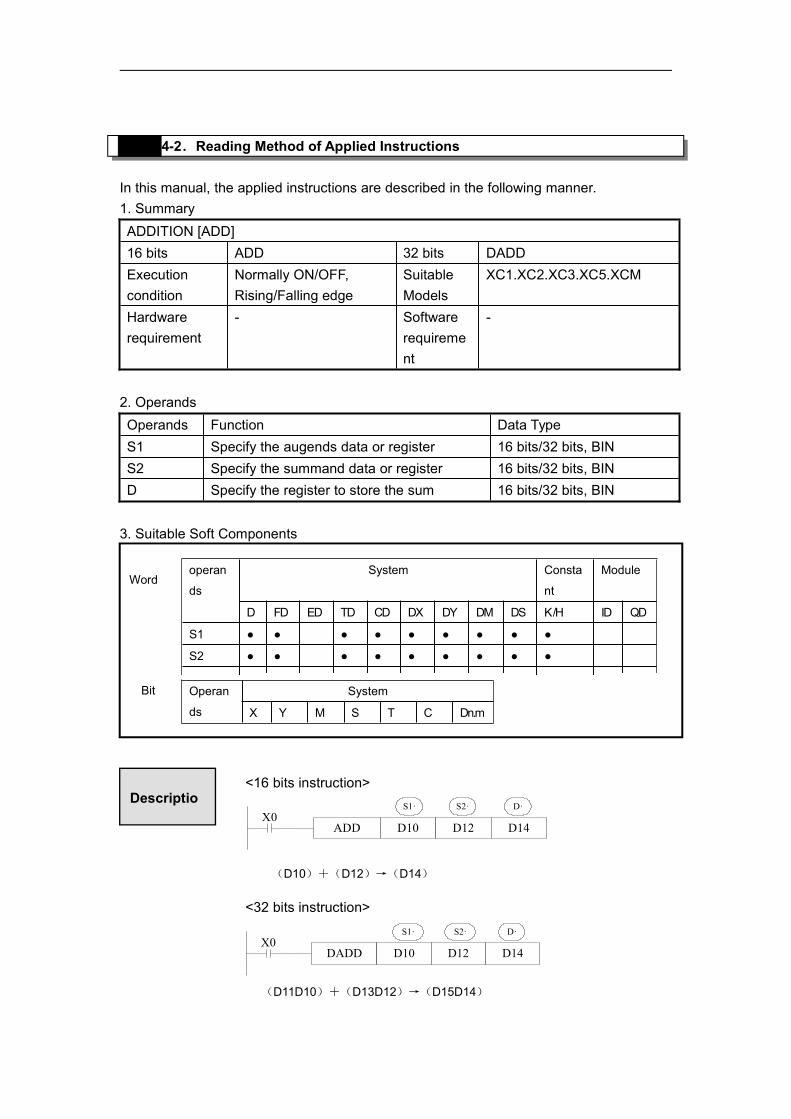
4-2.Reading Method of Applied Instructions
In this manual, the applied instructions are described in the following manner.1. SummaryADDITION [ADD]16 bits ADD 32 bits DADDExecutioncondition
Normally ON/OFF,Rising/Falling edge
SuitableModels
XC1.XC2.XC3.XC5.XCM
Hardwarerequirement
- Softwarerequirement
-
2. OperandsOperands Function Data TypeS1 Specify the augends data or register 16 bits/32 bits, BINS2 Specify the summand data or register 16 bits/32 bits, BIND Specify the register to store the sum 16 bits/32 bits, BIN
3. Suitable Soft Components
<16 bits instruction>
ADD D10 D12 D14X0
S1· S2· D·
<32 bits instruction>
DADD D10 D12 D14X0
S1· S2· D·
Wordoperan
ds
System Consta
nt
Module
D FD ED TD CD DX DY DM DS K/H ID QD
S1 ● ● ● ● ● ● ● ● ●
S2 ● ● ● ● ● ● ● ● ●
D ● ● ● ● ● ● ●Bit Operan
ds
System
X Y M S T C Dn.m
Descriptio
(D10)+(D12)→(D14)
(D11D10)+(D13D12)→(D15D14)
The data contained within the two source devices are combined and total is storedin the specified destination device. Each data’s highest bit is the sign bit, 0 stands forpositive, 1 stand for negative. All calculations are algebraic processed. (5+ (-8) = -3).
If the result of a calculations is “0”, the “0’ flag acts. If the result exceeds 323,767(16bits limit) or 2,147,483,648 (32 bits limit), the carry flag acts. (Refer to the next page).If the result exceeds -323,768 (16 bits limit) or -2,147,483,648 (32 bits limit ) , theborrow flag acts (Refer to the next page)
When carry on 32 bits operation, word device’s 16 bits are assigned, the devicefollow closely the preceding device’s ID will be the high bits. To avoid ID repetition,we recommend you assign device’s ID to be even ID.
The same device may be used a source and a destination. If this is the case then theresult changes after every scan cycle. Please note this point.
Flag Name Function
M8020 ZeroON:the calculate result is zeroOFF:the calculate result is not zero
M8021 Borrow
ON : the calculate result is over 32767(16bits) or2147483647(32bits)OFF : the calculate result is not over 32767(16bits) or2147483647(32bits)
M8022 Carry
ON : the calculate result is over 32767(16bits) or2147483647(32bits)OFF : the calculate result is not over 32767(16bits) or2147483647(32bits)
Instruction D(NUM) Object data
Related
The assignment of the dataThe data register of XC series PLC is a single word (16 bit) dataregister, single word data only engross one data register which isassigned by single word object instruction. The disposal bound is:Dec. –327, 68~327, 67, Hex. 0000~FFFF.
The
related
descriptio
D (NUM)Single word object instruction
→
Instruction D(NUM) Object data Object data
※1:Flag after executing the instruction, instructions without the direct flag will not display.※2: Source operand, its content won’t change after executing the instruction※3: Destinate operand, its content changes with the execution of the instruction※4:Tell the instruction’s basic action, using way, applied example, extend function, noteitems etc.
4-3.Program Flow Instructions
Mnemonic Instruction’s name ChapterCJ Condition Jump 4-3-1CALL Call subroutine 4-3-2SRET Subroutine return 4-3-2STL Flow start 4-3-3STLE Flow end 4-3-3SET Open the assigned flow, close the current flow (flow
jump)4-3-3
ST Open the assigned flow, not close the current flow(Open the new flow)
4-3-3
FOR Start of a FOR-NEXT loop 4-3-4NEXT End of a FOR-NEXT loop 4-3-4FEND First End 4-3-5END Program End 4-3-5
Double word(32 bit)engrosses two data register, it’s composed by two consecutive dataregisters, the first one is assigned by double word object instruction. The disposebound is: Dec. -214, 748, 364, 8~214, 748, 364, 7, Hex. 00000000~FFFFFFFF.
D (NUM+1) D (NUM)Double word object instruction→
The denote way of 32 bits instructionIf an instruction can not only be 16 bits but also be 32 bits, then the denote methodfor 32 bits instruction is to add a “D” before 16 bits instruction.E.g: ADD D0 D2 D4 denotes two 16 bits data adds
DADD D10 D12 D14 denotes two 32 bits data adds
S·
D·
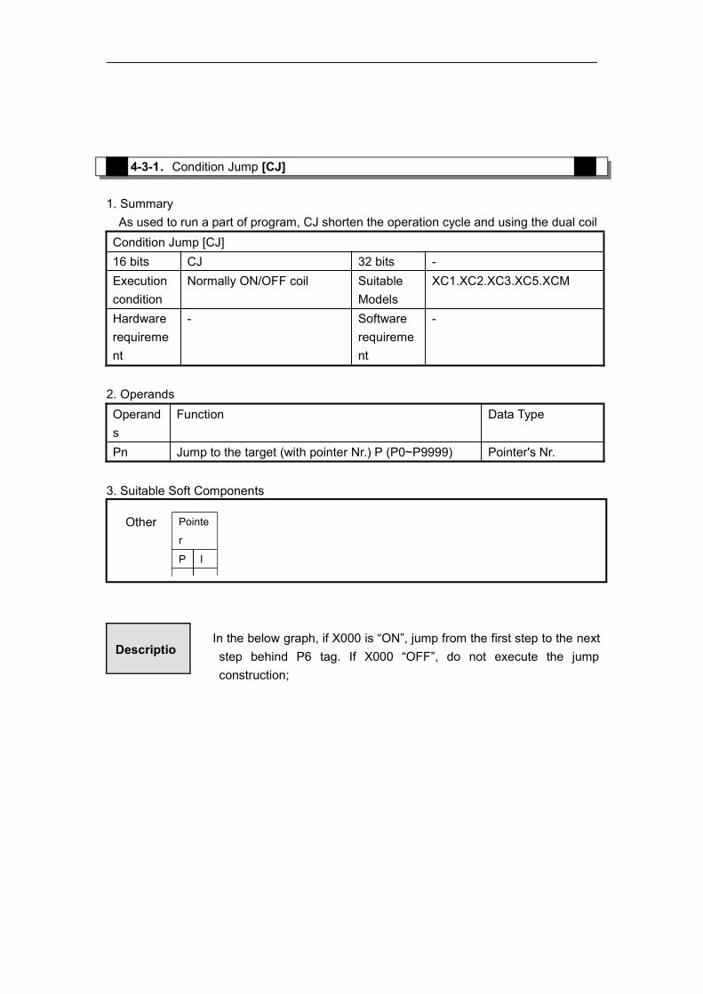
4-3-1.Condition Jump [CJ]
1. SummaryAs used to run a part of program, CJ shorten the operation cycle and using the dual coilCondition Jump [CJ]16 bits CJ 32 bits -Executioncondition
Normally ON/OFF coil SuitableModels
XC1.XC2.XC3.XC5.XCM
Hardwarerequirement
- Softwarerequirement
-
2. OperandsOperands
Function Data Type
Pn Jump to the target (with pointer Nr.) P (P0~P9999) Pointer's Nr.
3. Suitable Soft Components
In the below graph, if X000 is “ON”, jump from the first step to the nextstep behind P6 tag. If X000 “OFF”, do not execute the jumpconstruction;
Pointe
r
P I
●
Other
Descriptio
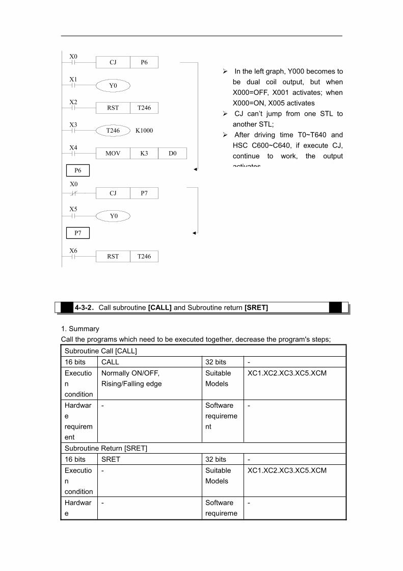
CJ
Y0
X0
X1
X3
X4
X0
RST
T246 K1000
MOV
CJ
X2
X5
X6
P6
T246
K3 D0
P7
T246RST
Y0
P6
P7
4-3-2.Call subroutine [CALL] and Subroutine return [SRET]
1. SummaryCall the programs which need to be executed together, decrease the program's steps;Subroutine Call [CALL]16 bits CALL 32 bits -Executioncondition
Normally ON/OFF,Rising/Falling edge
SuitableModels
XC1.XC2.XC3.XC5.XCM
Hardwarerequirement
- Softwarerequirement
-
Subroutine Return [SRET]16 bits SRET 32 bits -Executioncondition
- SuitableModels
XC1.XC2.XC3.XC5.XCM
Hardware
- Softwarerequireme
-
In the left graph, Y000 becomes tobe dual coil output, but whenX000=OFF, X001 activates; whenX000=ON, X005 activates
CJ can’t jump from one STL toanother STL;
After driving time T0~T640 andHSC C600~C640, if execute CJ,continue to work, the outputactivates.

requirement
nt
2. OperandsOperands
Function Data Type
Pn Jump to the target (with pointer Nr.) P(P0~P9999)
Pointer's Nr.
3. Suitable Soft Components
CALLX0
FEND
SRET
END
P10
P10
4-3-3.Flow [SET]. [ST]. [STL]. [STLE]
1、SummaryInstructions to specify the start, end, open, close of a flow;Open the specified flow, close the local flow [SET]16 bits SET 32 bits -Execution Normally ON/OFF, Suitable XC1.XC2.XC3.XC5.XCM
Others
Pointe
r
P I
●
Main
Program
Subroutine
If X000= “ON”, executethe call instruction andjump to the step taggedby P10. After executingthe subroutine, return theoriginal step via SRETinstruction. Program thetag with FENDinstruction (will describethis instruction later)
In the subroutine 9 timescall is allowed, so totallythere can be 10 nestings.
Descriptio

condition Rising/Falling edge ModelsHardwarerequirement
- Softwarerequirement
-
Open the specified flow, not close the local flow [ST]16 bits ST 32 bits -Executioncondition
Normally ON/OFF,Rising/Falling edge
SuitableModels
XC1.XC2.XC3.XC5.XCM
Hardwarerequirement
- Softwarerequirement
-
Flow starts [STL]16 bits STL 32 bits -Executioncondition
- SuitableModels
XC1.XC2.XC3.XC5.XCM
Hardwarerequirement
- Softwarerequirement
-
Flow ends [STLE]16 bits STLE 32 bits -Executioncondition
- SuitableModels
XC1.XC2.XC3.XC5.XCM
Hardwarerequirement
- Softwarerequirement
-
2. OperandsOperands Function Data TypeSn Jump to the target flow S Flow ID
3. Suitable Soft Components
Operan
ds
System
X Y M S T C Dn.m
Sn ●
Bit
Descriptio
STL and STLE should be used in pairs. STL represents the start of a flow; STLErepresents the end of a flow.
After executing of SET Sxxx instruction, the flow specified by these instructions isON.
After executing RST Sxxx instruction, the specified flow is OFF. In flow S0, SET S1 closes the current flow S0, open flow S1. In flow S0, ST S2 opens the flow S2, but don’t close flow S0. When flow turns from ON to be OFF, reset OUT、PLS、PLF、not accumulate timer etc,
which belong to the flow. ST instruction is usually used when a program needs to run more flows at the same
time. After executing of SET Sxxx instruction, the pulse instructions will be closed
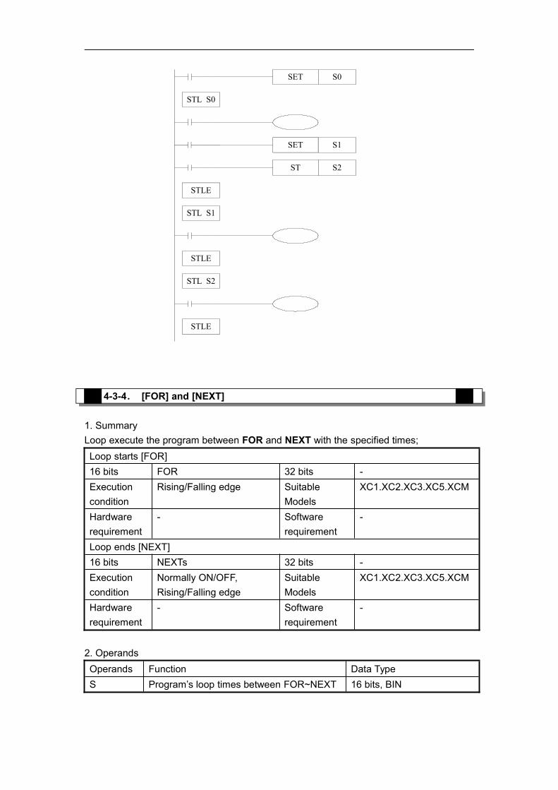
SET S0
STL S0
SET S1
ST S2
STL S1
STLE
STLE
STL S2
STLE
4-3-4. [FOR] and [NEXT]
1. SummaryLoop execute the program between FOR and NEXT with the specified times;Loop starts [FOR]16 bits FOR 32 bits -Executioncondition
Rising/Falling edge SuitableModels
XC1.XC2.XC3.XC5.XCM
Hardwarerequirement
- Softwarerequirement
-
Loop ends [NEXT]16 bits NEXTs 32 bits -Executioncondition
Normally ON/OFF,Rising/Falling edge
SuitableModels
XC1.XC2.XC3.XC5.XCM
Hardwarerequirement
- Softwarerequirement
-
2. OperandsOperands Function Data TypeS Program’s loop times between FOR~NEXT 16 bits, BIN
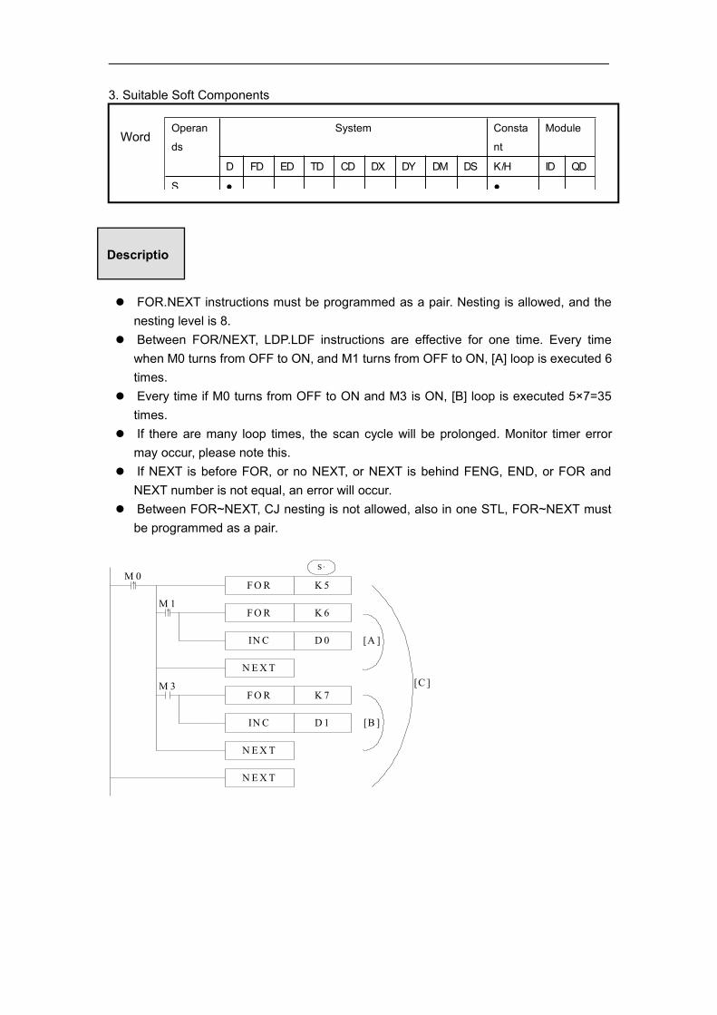
3. Suitable Soft Components
FOR.NEXT instructions must be programmed as a pair. Nesting is allowed, and thenesting level is 8.
Between FOR/NEXT, LDP.LDF instructions are effective for one time. Every timewhen M0 turns from OFF to ON, and M1 turns from OFF to ON, [A] loop is executed 6times.
Every time if M0 turns from OFF to ON and M3 is ON, [B] loop is executed 5×7=35times.
If there are many loop times, the scan cycle will be prolonged. Monitor timer errormay occur, please note this.
If NEXT is before FOR, or no NEXT, or NEXT is behind FENG, END, or FOR andNEXT number is not equal, an error will occur.
Between FOR~NEXT, CJ nesting is not allowed, also in one STL, FOR~NEXT mustbe programmed as a pair.
F O R K 6
IN C D 0
N E X T
F O R K 7
IN C D 1
N E X T
N E X T
F O R K 5M 0
M 3
M 1
[A ]
[B ]
[C ]
S ·
Operan
ds
System Consta
nt
Module
D FD ED TD CD DX DY DM DS K/H ID QD
S ● ●
Word
Descriptio

4-3-5. [FEND] and [END]
1. SummaryFEND means the main program ends, while END means program ends;main program ends [FEND]Executioncondition
- Suitable Models XC1.XC2.XC3.XC5.XCM
Hardwarerequirement
- Softwarerequirement
-
program ends [END]Executioncondition
- Suitable Models XC1.XC2.XC3.XC5.XCM
Hardwarerequirement
- Softwarerequirement
-
2. OperandsOperands
Function Data Type
None - -
3. Suitable Soft Components
Even though [FEND] instruction represents the end of the main program,if execute this instruction, the function is same with END. Execute theoutput/input disposal, monitor the refresh of the timer, and return to the0th step.
None
Descriptio
If program the tag of CALL instruction behind FEND instruction, there must beSRET instruction. If the interrupt pointer program behind FEND instruction, theremust be IRET instruction.
After executing CALL instruction and before executing SRET instruction, ifexecute FEND instruction; or execute FEND instruction after executing FORinstruction and before executing NEXT, then an error will occur.
In the condition of using many FEND instruction, please compile routine orsubroutine between the last FEND instruction and END instruction.
4-4. Data compare function
Mnemonic Function ChapterLD= LD activates when(S1)=(S2) 4-4-1LD> LD activates when(S1)>(S2) 4-4-1LD< LD activates when(S1)<(S2) 4-4-1LD<> LD activates when(S1)≠(S2) 4-4-1LD<= LD activates when(S1)≤(S2) 4-4-1LD>= LD activates when(S1)≥(S2) 4-4-1AND= AND activates when(S1)=(S2) 4-4-2AND> AND activates when(S1)>(S2) 4-4-2AND< AND activates when(S1)<(S2) 4-4-2AND<> AND activates when(S1)≠(S2) 4-4-2AND<= AND activates when(S1)≤(S2) 4-4-2AND>= AND activates when(S1)≥(S2) 4-4-2OR= OR activates when(S1)=(S2) 4-4-3OR> OR activates when(S1)>(S2) 4-4-3OR< OR activates when(S1)<(S2) 4-4-3OR<> OR activates when(S1)≠(S2) 4-4-3OR<= OR activates when(S1)≤(S2) 4-4-3OR>= OR activates when(S1)≥(S2) 4-4-3
4-4-1.LD Compare [LD□]
1. SummaryLD□ is the point compare instruction connected with the generatrix.LD Compare [LD□]16 bits As below 32 bits As belowExecution - Suitable XC1.XC2.XC3.XC5.XCM
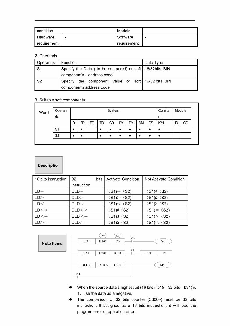
condition ModelsHardwarerequirement
- Softwarerequirement
-
2. OperandsOperands Function Data TypeS1 Specify the Data ( to be compared) or soft
component’s address code16/32bits, BIN
S2 Specify the component value or softcomponent’s address code
16/32 bits, BIN
3. Suitable soft components
16 bits instruction 32 bitsinstruction
Activate Condition Not Activate Condition
LD= DLD= (S1)=(S2) (S1)≠(S2)LD> DLD> (S1)>(S2) (S1)≤(S2)LD< DLD< (S1)<(S2) (S1)≥(S2)LD<> DLD<> (S1)≠(S2) (S1)=(S2)LD<= DLD<= (S1)≤(S2) (S1)>(S2)LD>= DLD>= (S1)≥(S2) (S1)<(S2)
LD> D200 K-30 SET Y1
DLD> K68899 C300 M50
X1
M4
S1· S2·
LD= K100 C0 Y0X0
Operan
ds
System Consta
nt
Module
D FD ED TD CD DX DY DM DS K/H ID QD
S1 ● ● ● ● ● ● ● ● ●
S2 ● ● ● ● ● ● ● ● ●
Word
Descriptio
When the source data’s highest bit (16 bits:b15,32 bits:b31) is1,use the data as a negative.
The comparison of 32 bits counter (C300~) must be 32 bitsinstruction. If assigned as a 16 bits instruction, it will lead theprogram error or operation error.
。
Note Items
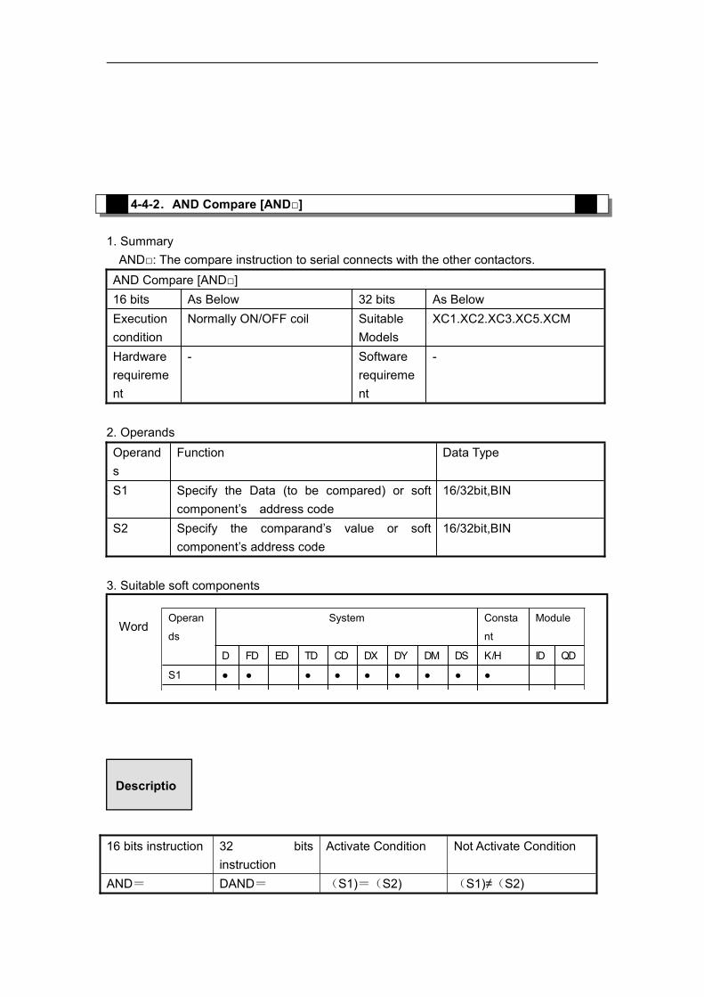
4-4-2.AND Compare [AND□]
1. SummaryAND□: The compare instruction to serial connects with the other contactors.AND Compare [AND□]16 bits As Below 32 bits As BelowExecutioncondition
Normally ON/OFF coil SuitableModels
XC1.XC2.XC3.XC5.XCM
Hardwarerequirement
- Softwarerequirement
-
2. OperandsOperands
Function Data Type
S1 Specify the Data (to be compared) or softcomponent’s address code
16/32bit,BIN
S2 Specify the comparand’s value or softcomponent’s address code
16/32bit,BIN
3. Suitable soft components
16 bits instruction 32 bitsinstruction
Activate Condition Not Activate Condition
AND= DAND= (S1)=(S2) (S1)≠(S2)
Operan
ds
System Consta
nt
Module
D FD ED TD CD DX DY DM DS K/H ID QD
S1 ● ● ● ● ● ● ● ● ●
S2 ● ● ● ● ● ● ● ● ●
Word
Descriptio
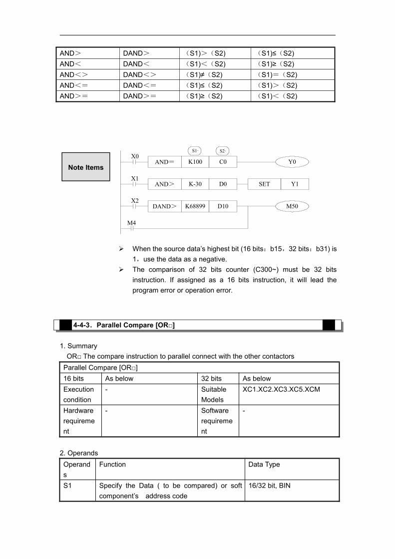
AND> DAND> (S1)>(S2) (S1)≤(S2)AND< DAND< (S1)<(S2) (S1)≥(S2)AND<> DAND<> (S1)≠(S2) (S1)=(S2)AND<= DAND<= (S1)≤(S2) (S1)>(S2)AND>= DAND>= (S1)≥(S2) (S1)<(S2)
AND= K100 C0 Y0
AND> D0K-30 SET Y1
DAND> K68899 D10 M50
X1
M4
X0
X2
S1· S2·
4-4-3.Parallel Compare [OR□]
1. SummaryOR□ The compare instruction to parallel connect with the other contactorsParallel Compare [OR□]16 bits As below 32 bits As belowExecutioncondition
- SuitableModels
XC1.XC2.XC3.XC5.XCM
Hardwarerequirement
- Softwarerequirement
-
2. OperandsOperands
Function Data Type
S1 Specify the Data ( to be compared) or softcomponent’s address code
16/32 bit, BIN
When the source data’s highest bit (16 bits:b15,32 bits:b31) is1,use the data as a negative.
The comparison of 32 bits counter (C300~) must be 32 bitsinstruction. If assigned as a 16 bits instruction, it will lead theprogram error or operation error.
Note Items
S2 Specify the comparand’s value or softcomponent’s address code
16/32 bit, BIN
3. Suitable soft components
16 bits instruction 32 bits instruction Activate Condition Not Activate ConditionOR= DOR= (S1)=(S2) (S1)≠(S2)OR> DOR> (S1)>(S2) (S1)≤(S2)OR< DOR< (S1)<(S2) (S1)≥(S2)OR<> DOR<> (S1)≠(S2) (S1)=(S2)OR<= DOR<= (S1)≤(S2) (S1)>(S2)OR>= DOR>= (S1)≥(S2) (S1)<(S2)
OR= K100 C0
Y0
DOR> K68899D10
M50M4
X0
X2
S1· S2·
4-5.Data Move
Operan
ds
System Consta
nt
Module
D FD ED TD CD DX DY DM DS K/H ID QD
S1 ● ● ● ● ● ● ● ● ●
S2 ● ● ● ● ● ● ● ● ●
Word
Description
When the source data’s highest bit (16 bits:b15,32 bits:b31) is1,use the data as a negative.
The comparison of 32 bits counter (C300~) must be 32 bitsinstruction. If assigned as a 16 bits instruction, it will lead theprogram error or operation error.
Note Items
Mnemonic Function Chapter
CMP Data compare 4-5-1ZCP Data zone compare 4-5-2MOV Move 4-5-3BMOV Data block move 4-5-4PMOV Data block move (with faster speed) 4-5-5FMOV Fill move 4-5-6FWRT FlashROM written 4-5-7MSET Zone set 4-5-8ZRST Zone reset 4-5-9SWAP The high and low byte of the
destinated devices are exchanged4-5-10
XCH Exchange 4-5-11
4-5-1.Data Compare [CMP]
1. SummaryCompare the two specified Data, output the result.Data compare [CMP]16 bits CMP 32 bits DCMPExecutioncondition
Normally ON/OFF,rising/falling edge
SuitableModels
XC1.XC2.XC3.XC5.XCM
Hardwarerequirement
- Softwarerequirement
-
2. OperandsOperands
Function Data Type
S1 Specify the data (to be compared) or softcomponent’s address code
16 bit, BIN
S Specify the comparand’s value or softcomponent’s address code
16 bit, BIN
D Specify the compare result’s address code bit
3. Suitable soft component
Word Operan
ds
System Consta
nt
Module
D FD ED TD CD DX DY DM DS K/H ID QD
S1 ● ● ● ● ● ● ● ● ●
S ● ● ● ● ● ● ● ● ●
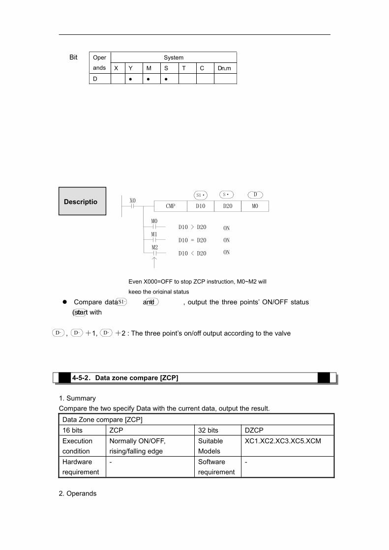
CMP D10 D20 M0
S1·
X0
M0
M1
M2
D10 > D20
S·
D10 = D20
D10 < D20
ON
ON
ON
D
4-5-2.Data zone compare [ZCP]
1. SummaryCompare the two specify Data with the current data, output the result.Data Zone compare [ZCP]16 bits ZCP 32 bits DZCPExecutioncondition
Normally ON/OFF,rising/falling edge
SuitableModels
XC1.XC2.XC3.XC5.XCM
Hardwarerequirement
- Softwarerequirement
-
2. Operands
Oper
ands
System
X Y M S T C Dn..m
D ● ● ●
Bit
Descriptio
Even X000=OFF to stop ZCP instruction, M0~M2 will
keep the original status
Compare data and , output the three points’ ON/OFF status(start with
S1· S·
D·
, +1, +2 : The three point’s on/off output according to the valveD· D· D·

4-5-3.MOV [MOV]
Operands Function Data TypeS1 Specify the down-limit Data (of the compare
stand) or soft component’s address code16 bit, BIN
S2 Specify the Up-limit Data (of the comparestand) or soft component’s address code
16 bit, BIN
S Specify the current data or soft component’saddress code
16 bit, BIN
D Specify the compare result’s data or softcomponent’s address code
bit
3. Suitable soft components
ZCP D20 D30 D0 M0
S1· S2· S· D·
X0
M0
M1
M2
D0 M0 ON
M1 ON
M2 ON
D0
D0
D20
D20 D31(分)
D31(分)
>
≤ ≤
>
WordOperan
ds
System Consta
nt
Module
D FD ED TD CD DX DY DM DS K/H ID QD
S1 ● ● ● ● ● ● ● ● ●
S2 ● ● ● ● ● ● ● ● ●
S ● ● ● ● ● ● ● ● ●Bit Oper
ands
System
X Y M S T C Dn..m
D ● ● ●
Even X000=OFF stop ZCP instruction,M0~M2 will
keep the original status
Descriptio
Compare data with and , output the three point’sON/OFF status according to the zone size.
, +1, +2 : the three point’s ON/OFF output according to theresult
S· D·
D·D·D·
S1 S2
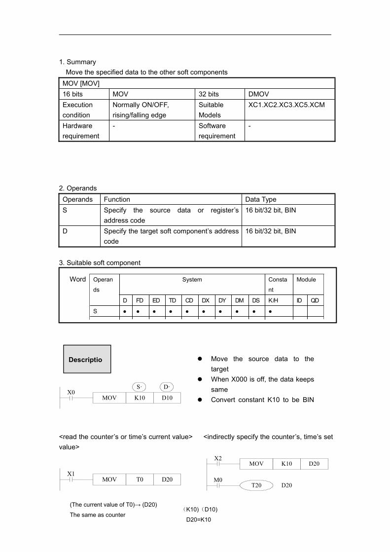
1. SummaryMove the specified data to the other soft componentsMOV [MOV]16 bits MOV 32 bits DMOVExecutioncondition
Normally ON/OFF,rising/falling edge
SuitableModels
XC1.XC2.XC3.XC5.XCM
Hardwarerequirement
- Softwarerequirement
-
2. OperandsOperands Function Data TypeS Specify the source data or register’s
address code16 bit/32 bit, BIN
D Specify the target soft component’s addresscode
16 bit/32 bit, BIN
3. Suitable soft component
MOV K10 D10X0
S· D·
<read the counter’s or time’s current value> <indirectly specify the counter’s, time’s setvalue>
MOV T0 D20X1
MOV K10 D20X2
M0T20 D20
Word Operan
ds
System Consta
nt
Module
D FD ED TD CD DX DY DM DS K/H ID QD
S ● ● ● ● ● ● ● ● ● ●
D ● ● ● ● ● ● ●
Descriptio Move the source data to thetarget
When X000 is off, the data keepssame
Convert constant K10 to be BIN
(K10)(D10)
D20=K10
(The current value of T0)→ (D20)
The same as counter
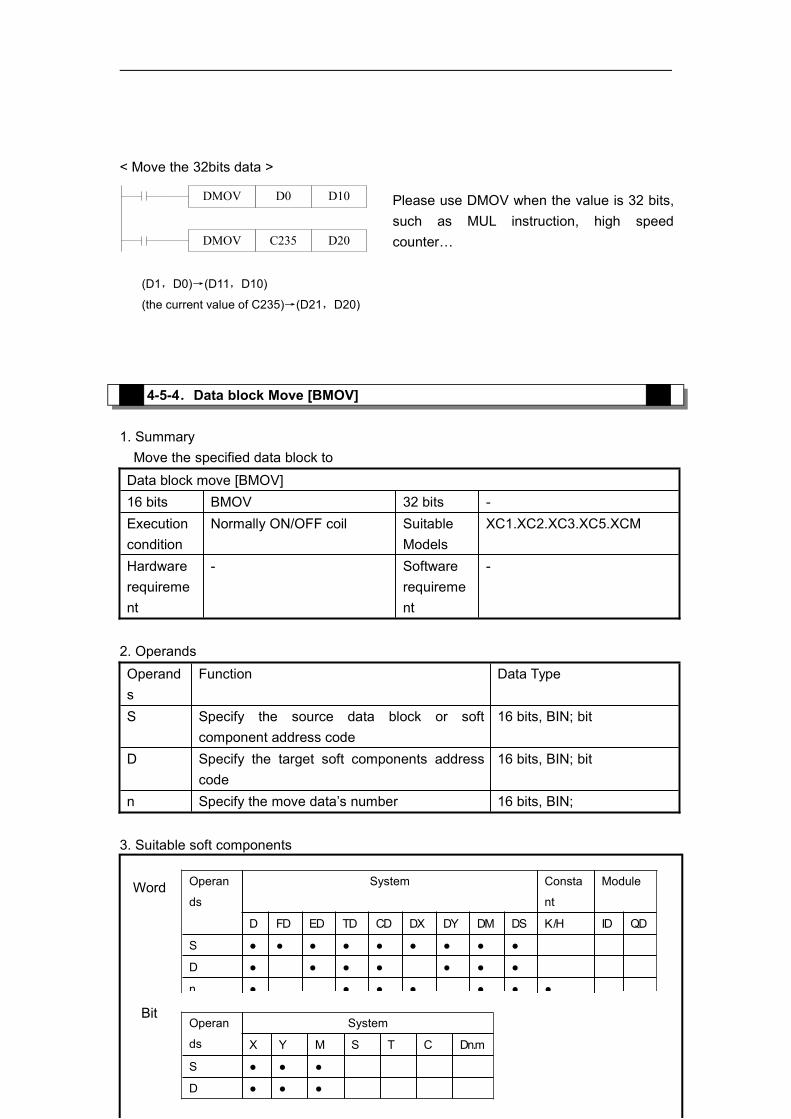
< Move the 32bits data >
DMOV D0 D10
DMOV C235 D20
4-5-4.Data block Move [BMOV]
1. SummaryMove the specified data block toData block move [BMOV]16 bits BMOV 32 bits -Executioncondition
Normally ON/OFF coil SuitableModels
XC1.XC2.XC3.XC5.XCM
Hardwarerequirement
- Softwarerequirement
-
2. OperandsOperands
Function Data Type
S Specify the source data block or softcomponent address code
16 bits, BIN; bit
D Specify the target soft components addresscode
16 bits, BIN; bit
n Specify the move data’s number 16 bits, BIN;
3. Suitable soft components
Please use DMOV when the value is 32 bits,such as MUL instruction, high speedcounter…
(D1,D0)→(D11,D10)
(the current value of C235)→(D21,D20)
Operan
ds
System Consta
nt
Module
D FD ED TD CD DX DY DM DS K/H ID QD
S ● ● ● ● ● ● ● ● ●
D ● ● ● ● ● ● ●
n ● ● ● ● ● ● ●
Word
BitOperan
ds
System
X Y M S T C Dn.m
S ● ● ●
D ● ● ●

Move the specified “n” data to the specified “n” soft components inthe form block.
BMOV D5 D10 K3X0
nS· D·
D5
D6
D7
D10
D11
D12
n=3
As the following picture, when the data address overlapped, theinstruction will do from 1 to 3.
BMOV D10 D11 K3
BMOV D10 D9 K3X1
X2
D10
D11
D12
D9
D10
D11
D10
D11
D12
D11
D12
D13
①
②
③
③
②
①
4-5-5.Data block Move [PMOV]
1. SummaryMove the specified data block to the other soft componentsData block move[PMOV]16 bits PMOV 32 bits -Executioncondition
Normally ON/OFF coil SuitableModels
XC1.XC2.XC3.XC5.XCM
Hardware - Software -
Descriptio

requirement requirement
2. OperandsOperands Function Data TypeS Specify the source data block or soft
component address code16 bits, BIN; bit
D Specify the target soft components addresscode
16 bits, BIN; bit
n Specify the move data’s number 16 bits, BIN;
3. Suitable soft components
Move the specified “n” data to the specified “n” soft components inform of block
PMOV D5 D10 K3X0
nS· D·
D5
D6
D7
D10
D11
D12
n=3
Operan
ds
System Consta
nt
Module
D FD ED TD CD DX DY DM DS K/H ID QD
S ● ● ● ● ● ● ● ● ●
D ● ● ● ● ● ● ●
n ● ● ● ● ● ● ●
Word
Oper
ands
system
X Y M S T C Dn.m
S ● ● ●
D ● ● ●
Bit
Descriptio
The function of PMOV and BMOV is mostly the same, but thePMOV has the faster speed
PMOV finish in one scan cycle, when executing PMOV , close allthe interruptions
Mistake many happen, if there is a repeat with source address andtarget address
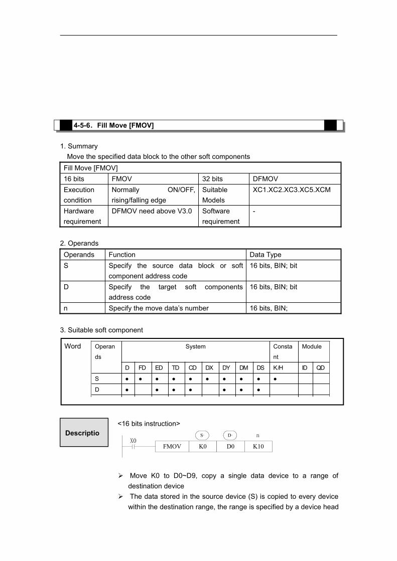
4-5-6.Fill Move [FMOV]
1. SummaryMove the specified data block to the other soft componentsFill Move [FMOV]16 bits FMOV 32 bits DFMOVExecutioncondition
Normally ON/OFF,rising/falling edge
SuitableModels
XC1.XC2.XC3.XC5.XCM
Hardwarerequirement
DFMOV need above V3.0 Softwarerequirement
-
2. OperandsOperands Function Data TypeS Specify the source data block or soft
component address code16 bits, BIN; bit
D Specify the target soft componentsaddress code
16 bits, BIN; bit
n Specify the move data’s number 16 bits, BIN;
3. Suitable soft component
<16 bits instruction>
FMOV K0 D0 K10X0
nS· D·
Move K0 to D0~D9, copy a single data device to a range ofdestination device
The data stored in the source device (S) is copied to every devicewithin the destination range, the range is specified by a device head
Word Operan
ds
System Consta
nt
Module
D FD ED TD CD DX DY DM DS K/H ID QD
S ● ● ● ● ● ● ● ● ● ●
D ● ● ● ● ● ● ●
n ● ● ● ● ● ● ●
Descriptio

address (D) and a quantity of consecutive elements (n). If the specified number of destination devices (n) exceeds the
available space at the destination location, then only the availabledestination devices will be written to.
<32 bits instruction >
DFMOV D0 D10 K3X0
nS· D·
Move D0.D1 to D10.D11:D12.D13:D14.D15.
<16 bits Fill Move > <32 bits Fill move>
K0 D0K0
n
D1K0
D2K0
D3K0
D4K0
D5K0
D6K0
D7K0
D8K0
D9K0

4-5-7.FlashROM Write [FWRT]
1. SummaryWrite the specified data to other soft componentsFlashROM Write [FWRT]16 bits FWRT 32 bits DFWRTExecutioncondition
rising/falling edge SuitableModels
XC1.XC2.XC3.XC5.XCM
Hardwarerequirement
- Softwarerequirement
-
2. OperandsOperands
Function Data Type
S The data write in the source or save in the softelement
16 bits/32 bits, BIN
D Write in target soft element 16 bits/32 bits, BIND1 Write in target soft element start address 16 bits/32 bits, BIND2 Write in data quantity bit
3. Suitable soft components
< Written of a word >
D0FWRT FD0X0
S· D·
<Written of double word> <Written of multi-word>
D0DFWRT FD0X1
S· D·
Operan
ds
System Consta
nt
Module
D FD ED TD CD DX DY DM DS K/H ID QD
S ● ● ● ● ● ● ● ● ●
D ●
D1 ●
D2 ● ● ● ● ● ● ● ●
Word
DescriptioWrite value in D0 into FD0
D0FWRT FD0X2
K3
S· D1· D2·
Write value in D0, D1 into FD0, FD1 Write value in D0, D1, and D2 into FD0,
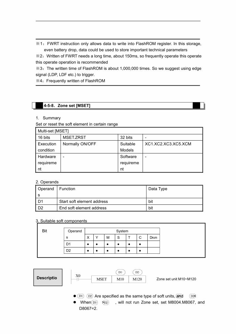
※1:FWRT instruction only allows data to write into FlashROM register. In this storage,even battery drop, data could be used to store important technical parameters
※2:Written of FWRT needs a long time, about 150ms, so frequently operate this operatethis operate operation is recommended※3:The written time of FlashROM is about 1,000,000 times. So we suggest using edgesignal (LDP, LDF etc.) to trigger.※4:Frequently written of FlashROM
4-5-8.Zone set [MSET]
1. SummarySet or reset the soft element in certain rangeMulti-set [MSET]16 bits MSET.ZRST 32 bits -Executioncondition
Normally ON/OFF SuitableModels
XC1.XC2.XC3.XC5.XCM
Hardwarerequirement
- Softwarerequirement
-
2. OperandsOperands
Function Data Type
D1 Start soft element address bitD2 End soft element address bit
3. Suitable soft components
MSET M10 M120
D1· D2·X0
Operand
s
System
X Y M S T C Dn.m
D1 ● ● ● ● ● ●
D2 ● ● ● ● ● ●
Bit
Zone set unit M10~M120Descriptio
Are specified as the same type of soft units, and < When > , will not run Zone set, set M8004.M8067, and
D8067=2.
D2·D1·D2·D1·
D2·D1·
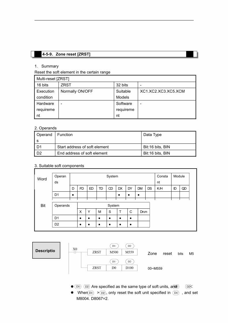
4-5-9.Zone reset [ZRST]
1. SummaryReset the soft element in the certain rangeMulti-reset [ZRST]16 bits ZRST 32 bits -Executioncondition
Normally ON/OFF SuitableModels
XC1.XC2.XC3.XC5.XCM
Hardwarerequirement
- Softwarerequirement
-
2. OperandsOperands
Function Data Type
D1 Start address of soft element Bit:16 bits, BIND2 End address of soft element Bit:16 bits, BIN
3. Suitable soft components
ZRST M500 M559
D0 D100
D1· D2·
D1· D2·
X0
ZRST
Operan
ds
System Consta
nt
Module
D FD ED TD CD DX DY DM DS K/H ID QD
D1 ● ● ● ●
D2 ● ● ● ● ●
Word
Operands System
X Y M S T C Dn.m
D1 ● ● ● ● ● ●
D2 ● ● ● ● ● ●
Bit
Zone reset bits M5
00~M559
Descriptio
Are specified as the same type of soft units, and <
When > , only reset the soft unit specified in , and setM8004. D8067=2.
D2·D1·D2·D1·
D1·D2·D1·

4-5-10.Swap the high and low byte [SWAP]
1. SummarySwap the high and low byteHigh and low byte swap [SWAP]16 bits SWAP 32 bits -Executioncondition
Normally ON/OFF SuitableModels
XC1.XC2.XC3.XC5.XCM
Hardwarerequirement
- Softwarerequirement
-
2. OperandsOperands
Function Data Type
S The address of the soft element 16 bits: BIN
3. Suitable soft components
SWAP D10
High 8-bit
D10
Low 8-bit
S·X0
OtherReset
As soft unit’s separate reset instruction, RST instruction can beused to bit unit Y, M, S and word unit T, C, D
As fill move for constant K0, 0 can be written into DX, DY, DM,DS, T, C, and D.
Word Operan
ds
System Consta
nt
Module
D FD ED TD CD DX DY DM DS K/H ID QD
S ● ● ●
Descriptio
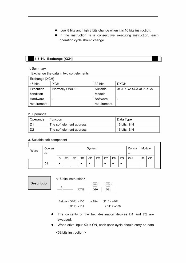
4-5-11.Exchange [XCH]
1. SummaryExchange the data in two soft elementsExchange [XCH]16 bits XCH 32 bits DXCHExecutioncondition
Normally ON/OFF SuitableModels
XC1.XC2.XC3.XC5.XCM
Hardwarerequirement
- Softwarerequirement
-
2. OperandsOperands Function Data TypeD1 The soft element address 16 bits, BIND2 The soft element address 16 bits, BIN
3. Suitable soft component
<16 bits instruction>
XCH D10 D11X0
D1· D2·
<32 bits instruction >
Low 8 bits and high 8 bits change when it is 16 bits instruction. If the instruction is a consecutive executing instruction, each
operation cycle should change.
Operan
ds
System Consta
nt
Module
D FD ED TD CD DX DY DM DS K/H ID QD
D1 ● ● ● ● ● ●
D2 ● ● ● ● ● ●
Word
Descriptio
Before(D10)=100 →After (D10)=101
(D11)=101 (D11)=100
The contents of the two destination devices D1 and D2 areswapped,
When drive input X0 is ON, each scan cycle should carry on dataexchange, please note.

DXCH D10 D20X0
D1· D2·
4-5-12.Floating move [EMOV]
1. SummarySend the floating number from one soft element to anotherFloating move [EMOV]16 bits - 32 bits EMOVExecutioncondition
Normally on/off, edge trigger Suitablemodels
XC2、XC3、XC5、XCM、XCC
Hardware V3.3 and higher Software V3.3 and higher
2. OperandsOperand Function TypeS Source soft element address 32 bits, BIND Destination soft element address 32 bits, BIN
3. Suitable soft element
<32 bits instruction>Binary floating → binary floating
(D1,D0)→(D11,D10)
X0 is ON, send the floating number from (D1, D0) to (D11, D10). X0 is OFF, the instruction doesn’t work
32 bits instruction [DXCH] swaps value composed by D10, D11 andthe value composed by D20, D21.
Operand System Constant Module
D FD ED TD CD DX DY DM DS K/H ID QD
S ● ● ● ● ● ● ●
D ● ● ● ●
Word
Descriptio
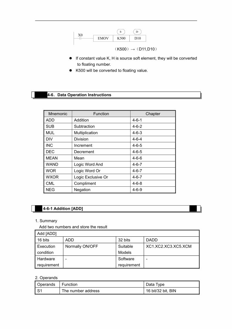
EMOV K500 D10X0
S· D·
(K500)→(D11,D10)
If constant value K, H is source soft element, they will be convertedto floating number.
K500 will be converted to floating value.
4-6.Data Operation Instructions
Mnemonic Function ChapterADD Addition 4-6-1SUB Subtraction 4-6-2MUL Multiplication 4-6-3DIV Division 4-6-4INC Increment 4-6-5DEC Decrement 4-6-5MEAN Mean 4-6-6WAND Logic Word And 4-6-7WOR Logic Word Or 4-6-7WXOR Logic Exclusive Or 4-6-7CML Compliment 4-6-8NEG Negation 4-6-9
4-6-1 Addition [ADD]
1. SummaryAdd two numbers and store the resultAdd [ADD]16 bits ADD 32 bits DADDExecutioncondition
Normally ON/OFF SuitableModels
XC1.XC2.XC3.XC5.XCM
Hardwarerequirement
- Softwarerequirement
-
2. OperandsOperands Function Data TypeS1 The number address 16 bit/32 bit, BIN
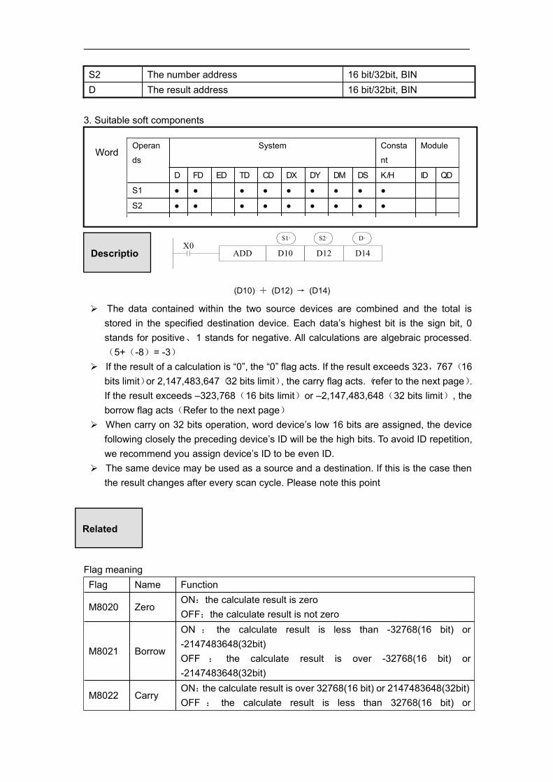
S2 The number address 16 bit/32bit, BIND The result address 16 bit/32bit, BIN
3. Suitable soft components
ADD D10 D12 D14X0
S1· S2· D·
The data contained within the two source devices are combined and the total isstored in the specified destination device. Each data’s highest bit is the sign bit, 0stands for positive、1 stands for negative. All calculations are algebraic processed.(5+(-8)= -3)
If the result of a calculation is “0”, the “0” flag acts. If the result exceeds 323,767(16bits limit)or 2,147,483,647(32 bits limit), the carry flag acts.(refer to the next page).If the result exceeds –323,768(16 bits limit)or –2,147,483,648(32 bits limit), theborrow flag acts(Refer to the next page)
When carry on 32 bits operation, word device’s low 16 bits are assigned, the devicefollowing closely the preceding device’s ID will be the high bits. To avoid ID repetition,we recommend you assign device’s ID to be even ID.
The same device may be used as a source and a destination. If this is the case thenthe result changes after every scan cycle. Please note this point
Flag meaningFlag Name Function
M8020 ZeroON:the calculate result is zeroOFF:the calculate result is not zero
M8021 Borrow
ON : the calculate result is less than -32768(16 bit) or-2147483648(32bit)OFF : the calculate result is over -32768(16 bit) or-2147483648(32bit)
M8022 CarryON:the calculate result is over 32768(16 bit) or 2147483648(32bit)OFF : the calculate result is less than 32768(16 bit) or
Operan
ds
System Consta
nt
Module
D FD ED TD CD DX DY DM DS K/H ID QD
S1 ● ● ● ● ● ● ● ● ●
S2 ● ● ● ● ● ● ● ● ●
D ● ● ● ● ● ●
Word
Descriptio
(D10) + (D12) → (D14)
Related

2147483648(32bit)
4-6-2.Subtraction [SUB]
1. SummarySub two numbers, store the resultSubtraction [SUB]16 bits SUB 32 bits DSUBExecutioncondition
Normally ON/OFF SuitableModels
XC1.XC2.XC3.XC5.XCM
Hardwarerequirement
- Softwarerequirement
-
2. OperandsOperands
Function Data Type
S1 The number address 16 bits /32 bits, BINS2 The number address 16 bits /32 bits, BIND The result address 16 bits /32 bits, BIN
3. Suitable soft component
SUB D10 D12 D14X0
S1· S2· D·
Operan
ds
System Consta
nt
Module
D FD ED TD CD DX DY DM DS K/H ID QD
S1 ● ● ● ● ● ● ● ● ●
S2 ● ● ● ● ● ● ● ● ●
D ● ● ● ● ● ●
Word
(D10)—(D12)→(D14)
Descriptio
Appoint the soft unit’s content; subtract the soft unit’s content appointed byin the format of algebra. The result will be stored in the soft unit appointed by .(5-(-8)=13)
The action of each flag, the appointment method of 32 bits operation’s soft unitsare both the same with the preceding ADD instruction.
The importance is: in the preceding program, if X0 is ON, SUB operation will beexecuted every scan cycle
S1· S2·
D·

The relationship of the flag’s action and vale’s positive/negative is shown below:
4-6-3.Multiplication [MUL]
1. SummaryMultiply two numbers, store the resultMultiplication [MUL]16 bits MUL 32 bits DMULExecutioncondition
Normally ON/OFF SuitableModels
XC1.XC2.XC3.XC5.XCM
Hardwarerequirement
- Softwarerequirement
-
2. OperandsOperands Function Data TypeS1 The number address 16 bits/32bits,BINS2 The number address 16 bits/32bits,BIND The result address 16 bits/32bits,BIN
3. Suitable soft component
Operan
ds
System Consta
nt
Module
D FD ED TD CD DX DY DM DS K/H ID QD
S1 ● ● ● ● ● ● ● ● ●
S2 ● ● ● ● ● ● ● ● ●
D ● ● ● ● ● ●
Word
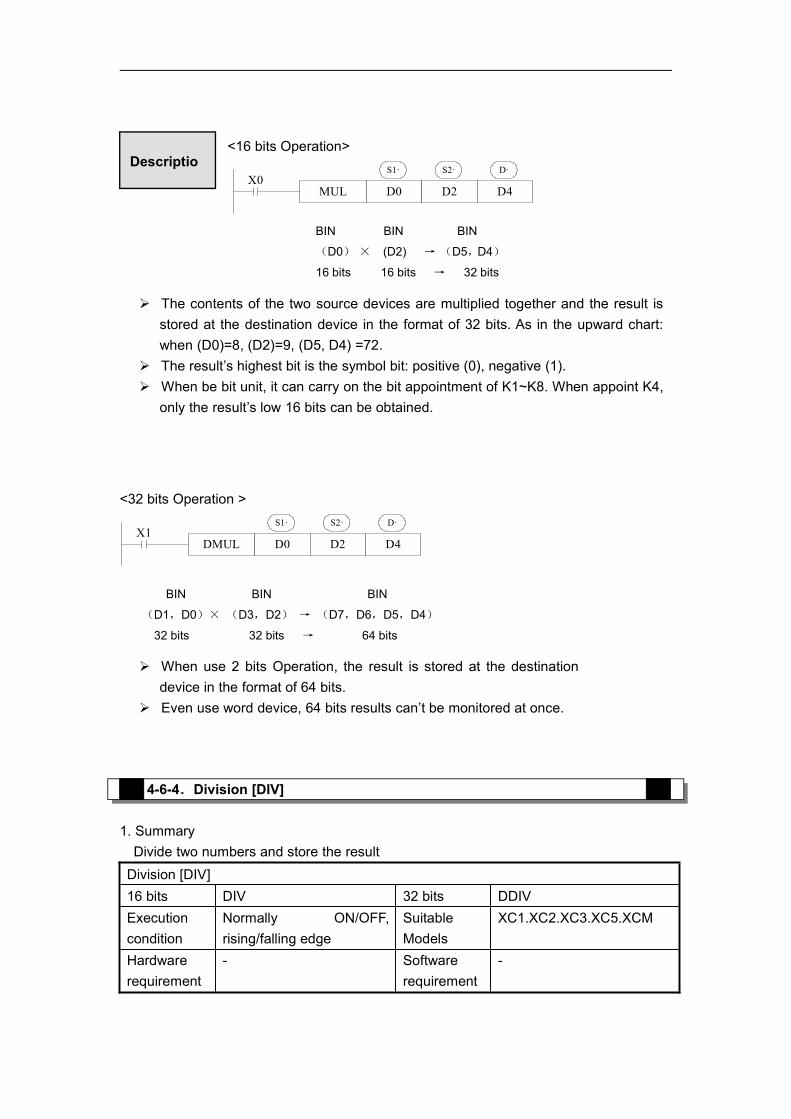
<16 bits Operation>
MUL D0 D2 D4X0
S1· S2· D·
<32 bits Operation >
X1DMUL D0 D2 D4
S1· S2· D·
4-6-4.Division [DIV]
1. SummaryDivide two numbers and store the resultDivision [DIV]16 bits DIV 32 bits DDIVExecutioncondition
Normally ON/OFF,rising/falling edge
SuitableModels
XC1.XC2.XC3.XC5.XCM
Hardwarerequirement
- Softwarerequirement
-
Descriptio
BIN BIN BIN
(D0) × (D2) → (D5,D4)
16 bits 16 bits → 32 bits
The contents of the two source devices are multiplied together and the result isstored at the destination device in the format of 32 bits. As in the upward chart:when (D0)=8, (D2)=9, (D5, D4) =72.
The result’s highest bit is the symbol bit: positive (0), negative (1). When be bit unit, it can carry on the bit appointment of K1~K8. When appoint K4,
only the result’s low 16 bits can be obtained.
BIN BIN BIN
(D1,D0)× (D3,D2) → (D7,D6,D5,D4)
32 bits 32 bits → 64 bits
When use 2 bits Operation, the result is stored at the destinationdevice in the format of 64 bits.
Even use word device, 64 bits results can’t be monitored at once.
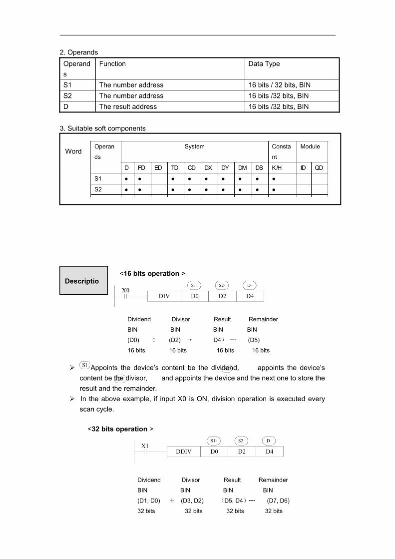
2. OperandsOperands
Function Data Type
S1 The number address 16 bits / 32 bits, BINS2 The number address 16 bits /32 bits, BIND The result address 16 bits /32 bits, BIN
3. Suitable soft components
<16 bits operation >
DIV D0 D2 D4X0
S1· S2· D·
<32 bits operation >
DDIV D0 D2 D4X1
S1· S2· D·
Operan
ds
System Consta
nt
Module
D FD ED TD CD DX DY DM DS K/H ID QD
S1 ● ● ● ● ● ● ● ● ●
S2 ● ● ● ● ● ● ● ● ●
D ● ● ● ● ● ●
Word
Dividend Divisor Result Remainder
BIN BIN BIN BIN
(D0) ÷ (D2) → D4) ┅ (D5)
16 bits 16 bits 16 bits 16 bits
Descriptio
Appoints the device’s content be the dividend, appoints the device’scontent be the divisor, and appoints the device and the next one to store theresult and the remainder.
In the above example, if input X0 is ON, division operation is executed everyscan cycle.
D·
S2·S1·
Dividend Divisor Result Remainder
BIN BIN BIN BIN
(D1, D0) ÷ (D3, D2) (D5, D4)┅ (D7, D6)
32 bits 32 bits 32 bits 32 bits

4-6-5.Increment [INC] & Decrement [DEC]
1. SummaryIncrease or decrease the numberIncrement 1[INC]16 bits INC 32 bits DINCExecutioncondition
Normally ON/OFF,rising/falling edge
SuitableModels
XC1.XC2.XC3.XC5.XCM
Hardwarerequirement
- Softwarerequirement
-
Increment 1[DEC]16 bits DEC 32 bits DDECExecutioncondition
Normally ON/OFF,rising/falling edge
SuitableModels
XC1.XC2.XC3.XC5.XCM
Hardwarerequirement
- Softwarerequirement
-
2. OperandsOperands Function Data TypeD The number address 16 bits / 32bits, BIN
3. Suitable soft components
The dividend is composed by the device appointed by and the next one. Thedivisor is composed by the device appointed by and the next one. The resultand the remainder are stored in the four sequential devices, the first one isappointed by
If the value of the divisor is 0, then an operation error is executed and theoperation of the DIV instruction is cancelled
S1·
S2·
D·
Word Operan
ds
System Consta
nt
Module
D FD ED TD CD DX DY DM DS K/H ID QD
D ● ● ● ● ● ●
The highest bit of the result and remainder is the symbol bit (positive: 0, negative: 1).When any of the dividend or the divisor is negative, then the result will be negative.When the dividend is negative, then the remainder will be negative.
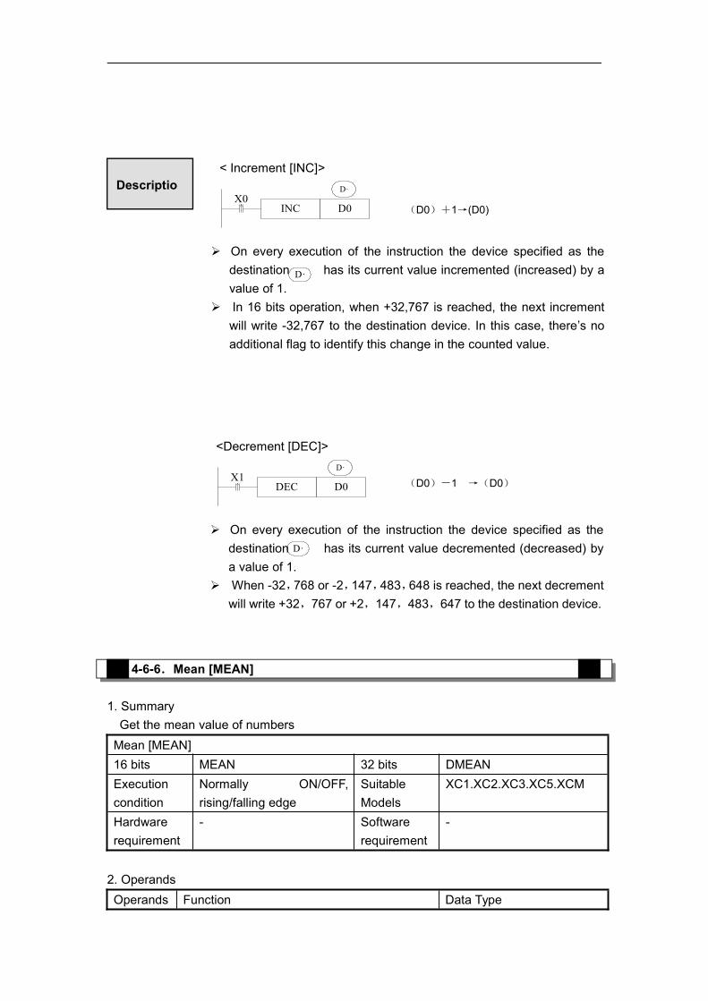
< Increment [INC]>
INC D0X0
D·
<Decrement [DEC]>
DEC D0X1
D·
4-6-6.Mean [MEAN]
1. SummaryGet the mean value of numbersMean [MEAN]16 bits MEAN 32 bits DMEANExecutioncondition
Normally ON/OFF,rising/falling edge
SuitableModels
XC1.XC2.XC3.XC5.XCM
Hardwarerequirement
- Softwarerequirement
-
2. OperandsOperands Function Data Type
Descriptio
(D0)+1→(D0)
On every execution of the instruction the device specified as thedestination has its current value incremented (increased) by avalue of 1.
In 16 bits operation, when +32,767 is reached, the next incrementwill write -32,767 to the destination device. In this case, there’s noadditional flag to identify this change in the counted value.
D·
(D0)-1 →(D0)
On every execution of the instruction the device specified as thedestination has its current value decremented (decreased) bya value of 1.
When -32,768 or -2,147,483,648 is reached, the next decrementwill write +32,767 or +2,147,483,647 to the destination device.
D·
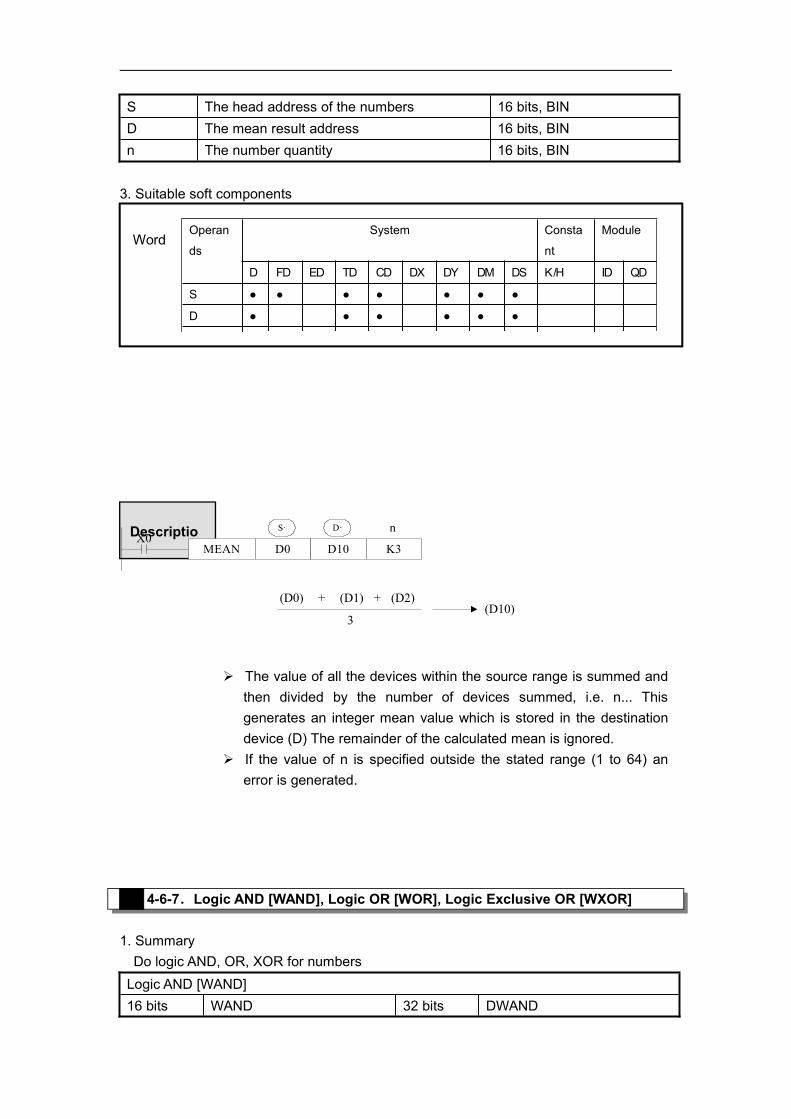
S The head address of the numbers 16 bits, BIND The mean result address 16 bits, BINn The number quantity 16 bits, BIN
3. Suitable soft components
(D0) + +
3(D10)
(D1) (D2)
4-6-7.Logic AND [WAND], Logic OR [WOR], Logic Exclusive OR [WXOR]
1. SummaryDo logic AND, OR, XOR for numbersLogic AND [WAND]16 bits WAND 32 bits DWAND
Operan
ds
System Consta
nt
Module
D FD ED TD CD DX DY DM DS K/H ID QD
S ● ● ● ● ● ● ●
D ● ● ● ● ● ●
n ●
Word
DescriptioMEAN D0 D10 K3
S· D·X0
n
The value of all the devices within the source range is summed andthen divided by the number of devices summed, i.e. n... Thisgenerates an integer mean value which is stored in the destinationdevice (D) The remainder of the calculated mean is ignored.
If the value of n is specified outside the stated range (1 to 64) anerror is generated.
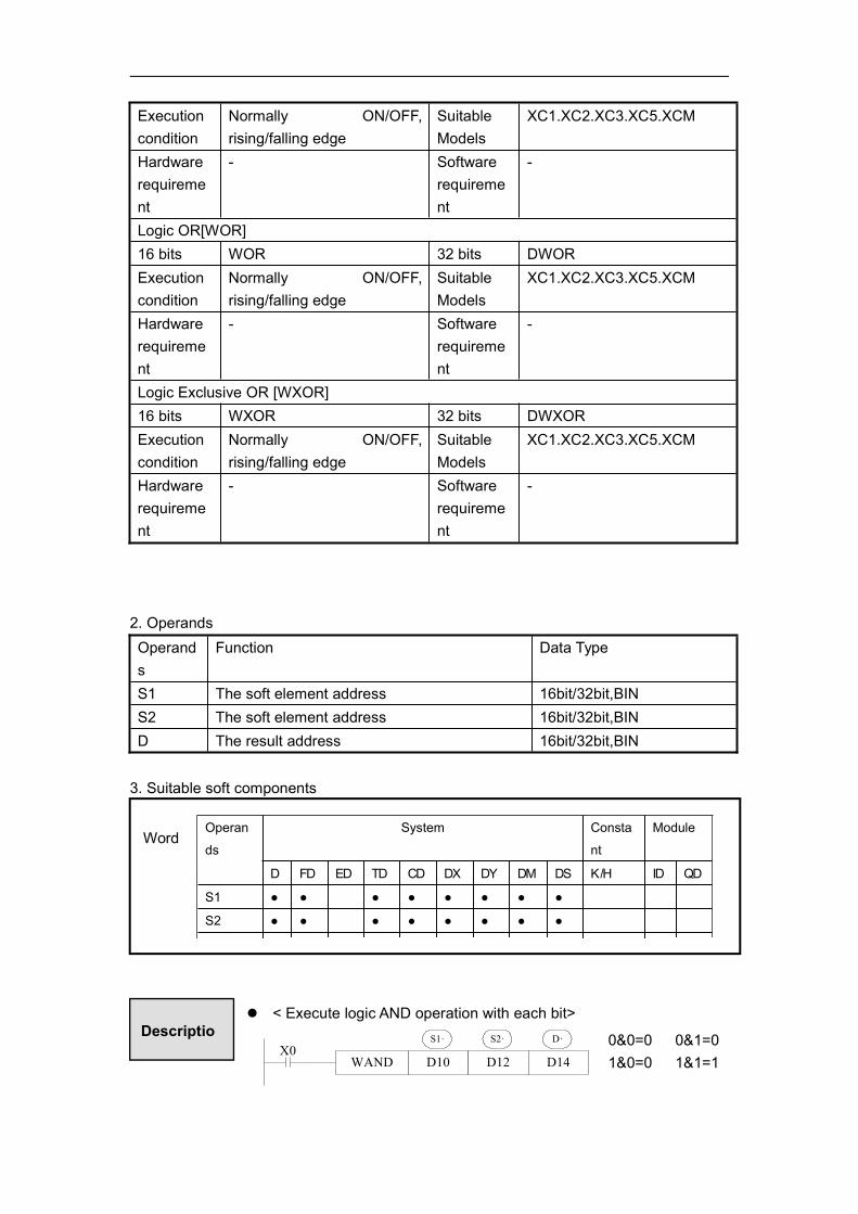
Executioncondition
Normally ON/OFF,rising/falling edge
SuitableModels
XC1.XC2.XC3.XC5.XCM
Hardwarerequirement
- Softwarerequirement
-
Logic OR[WOR]16 bits WOR 32 bits DWORExecutioncondition
Normally ON/OFF,rising/falling edge
SuitableModels
XC1.XC2.XC3.XC5.XCM
Hardwarerequirement
- Softwarerequirement
-
Logic Exclusive OR [WXOR]16 bits WXOR 32 bits DWXORExecutioncondition
Normally ON/OFF,rising/falling edge
SuitableModels
XC1.XC2.XC3.XC5.XCM
Hardwarerequirement
- Softwarerequirement
-
2. OperandsOperands
Function Data Type
S1 The soft element address 16bit/32bit,BINS2 The soft element address 16bit/32bit,BIND The result address 16bit/32bit,BIN
3. Suitable soft components
< Execute logic AND operation with each bit>
WAND D10 D12 D14
D·X0
S1· S2·
Operan
ds
System Consta
nt
Module
D FD ED TD CD DX DY DM DS K/H ID QD
S1 ● ● ● ● ● ● ● ●
S2 ● ● ● ● ● ● ● ●
D ● ● ● ● ● ●
Word
Descriptio 0&0=0 0&1=01&0=0 1&1=1

< Execute logic OR operation with each bit >
WOR D10 D12 D14
D·X0
S1· S2·
< Execute logic Exclusive OR operation with each bit >
WXOR D10 D12 D14
D·X0
S1· S2·
If use this instruction along with CML instruction, XOR NOT operationcould also be executed.
WXOR D10 D12 D14
D·X0
S1· S2·
CML D14 D14
4-6-8.Converse [CML]
1. SummaryConverse the phase of the numbersConverse [CML]16 bits CML 32 bits DCMLExecutioncondition
Normally ON/OFF,rising/falling edge
SuitableModels
XC1.XC2.XC3.XC5.XCM
Hardwarerequirement
- Softwarerequirement
-
2. OperandsOperands
Function Data Type
S Source number address 16 bits/32 bits, BIND Result address 16 bits/32 bits, BIN
3. Suitable soft components
0 or 0=0 0 or 1=11 or 0=1 1 or 1=1
0 xor 0=0 0 xor 1=11 xor 0=1 1 xor 1=0
Word Operan
ds
System Consta
nt
Module
D FD ED TD CD DX DY DM DS K/H ID QD
S1 ● ● ● ● ● ● ● ● ●
D ● ● ● ● ● ●
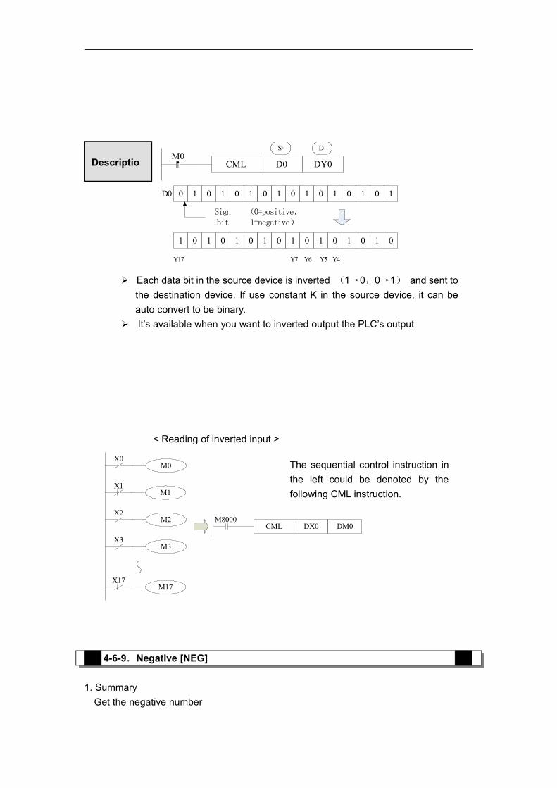
CML D0 DY0
S· D·M0↑
0 1 0 1 0 1 0 1 0 1 0 1 0 1 0 1
1 0 1 0 1 0 1 0 1 0 1 0 1 0 1 0
D0
Y17 Y7 Y6 Y5 Y4
Sign bit
(0=positive,1=negative)
< Reading of inverted input >
M0
M1
M2
M3
M17
CML DX0 DM0M8000
X0
X1
X2
X3
X17
4-6-9.Negative [NEG]
1. SummaryGet the negative number
Each data bit in the source device is inverted (1→0,0→1) and sent tothe destination device. If use constant K in the source device, it can beauto convert to be binary.
It’s available when you want to inverted output the PLC’s output
Descriptio
The sequential control instruction inthe left could be denoted by thefollowing CML instruction.

Negative [NEG]16 bits NEG 32 bits DNEGExecutioncondition
Normally ON/OFF,rising/falling edge
SuitableModels
XC1.XC2.XC3.XC5.XCM
Hardwarerequirement
- Softwarerequirement
-
2. OperandsOperands
Function Data Type
D The source number address 16 bits/ bits, BIN
3. Suitable soft components
NEG D10 (D10) +1 (D10)M0
D·
4-7.Shift Instructions
Mnemonic Function ChapterSHL Arithmetic shift left 4-7-1SHR Arithmetic shift right 4-7-1LSL Logic shift left 4-7-2
Operan
ds
System Consta
nt
Module
D FD ED TD CD DX DY DM DS K/H ID QD
D ● ● ● ● ● ●
Word
Descriptio
The bit format of the selected device is inverted, I.e. anyoccurrence of a “1’ becomes a “0” and any occurrence of “0”becomes “1”, when this is complete, a further binary 1 is addedto the bit format. The result is the total logic sigh change of theselected devices contents.
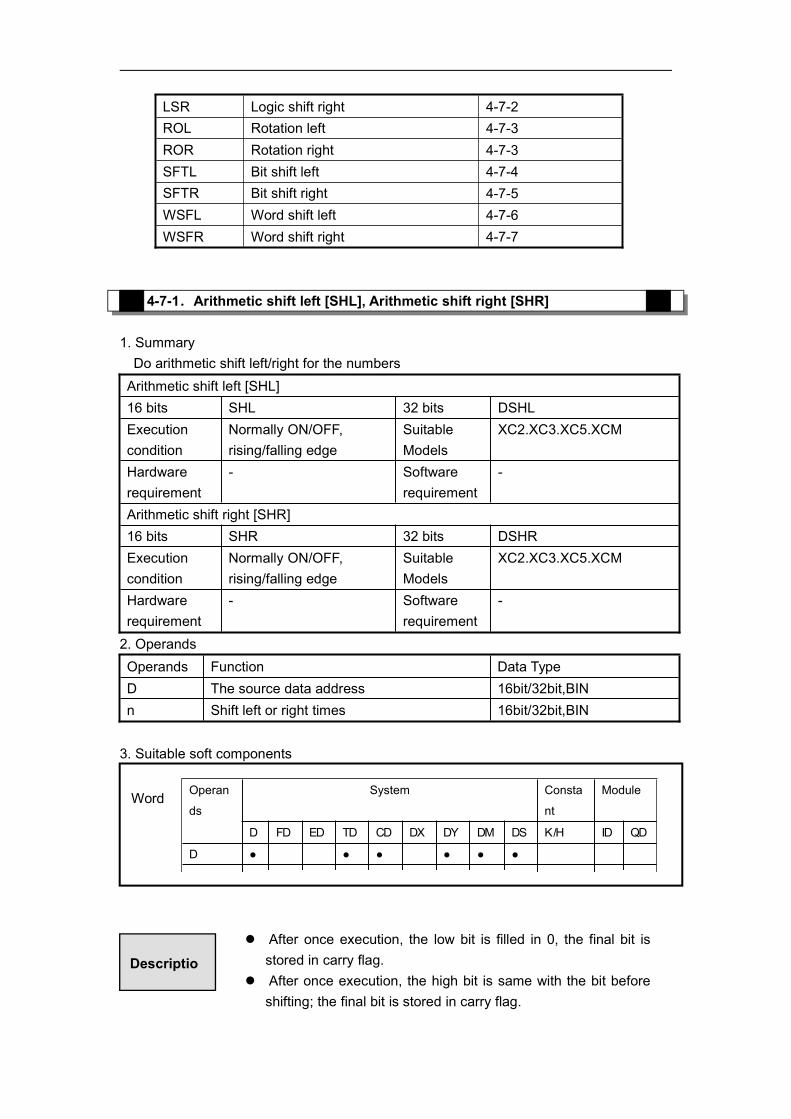
LSR Logic shift right 4-7-2ROL Rotation left 4-7-3ROR Rotation right 4-7-3SFTL Bit shift left 4-7-4SFTR Bit shift right 4-7-5WSFL Word shift left 4-7-6WSFR Word shift right 4-7-7
4-7-1.Arithmetic shift left [SHL], Arithmetic shift right [SHR]
1. SummaryDo arithmetic shift left/right for the numbersArithmetic shift left [SHL]16 bits SHL 32 bits DSHLExecutioncondition
Normally ON/OFF,rising/falling edge
SuitableModels
XC2.XC3.XC5.XCM
Hardwarerequirement
- Softwarerequirement
-
Arithmetic shift right [SHR]16 bits SHR 32 bits DSHRExecutioncondition
Normally ON/OFF,rising/falling edge
SuitableModels
XC2.XC3.XC5.XCM
Hardwarerequirement
- Softwarerequirement
-
2. OperandsOperands Function Data TypeD The source data address 16bit/32bit,BINn Shift left or right times 16bit/32bit,BIN
3. Suitable soft components
Operan
ds
System Consta
nt
Module
D FD ED TD CD DX DY DM DS K/H ID QD
D ● ● ● ● ● ●
n ●
Word
After once execution, the low bit is filled in 0, the final bit isstored in carry flag.
After once execution, the high bit is same with the bit beforeshifting; the final bit is stored in carry flag.
Descriptio
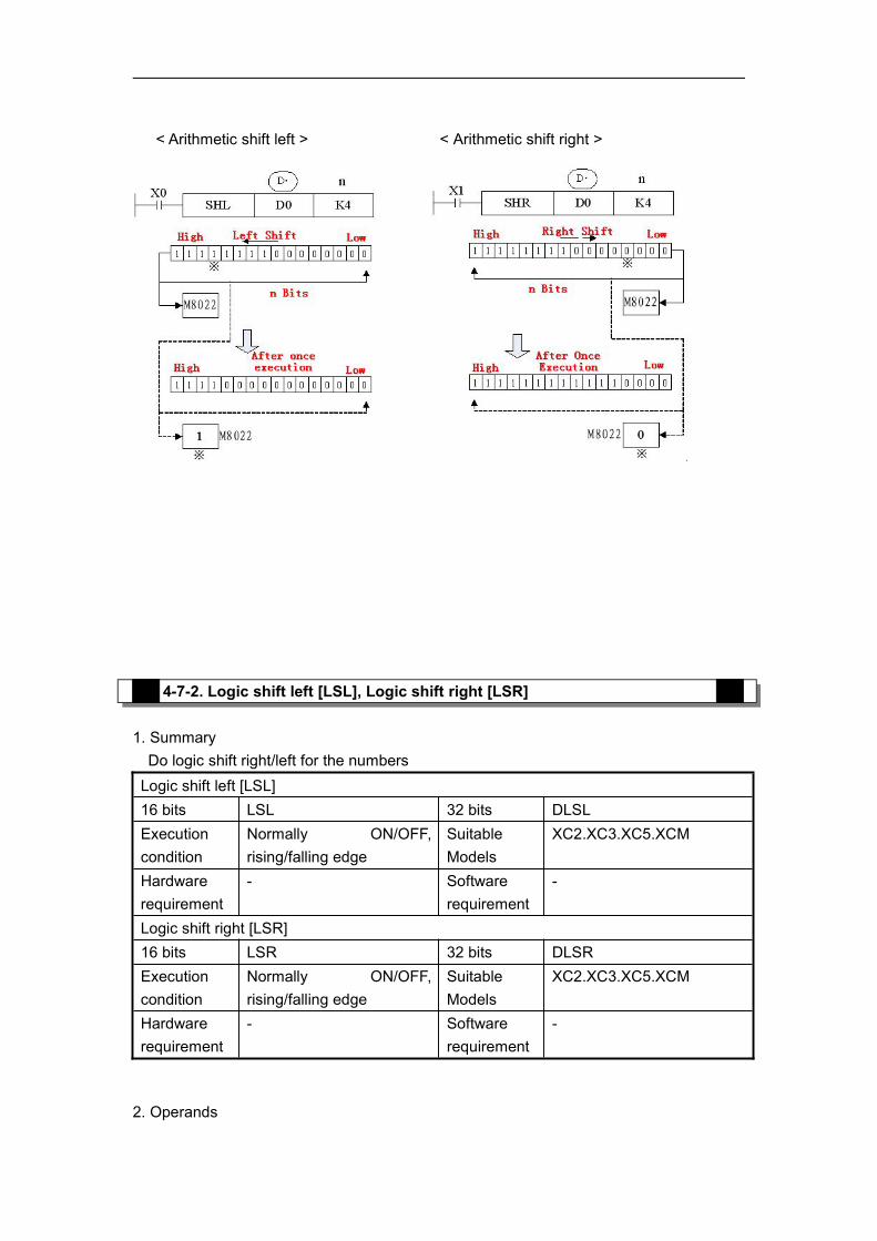
< Arithmetic shift left > < Arithmetic shift right >
4-7-2. Logic shift left [LSL], Logic shift right [LSR]
1. SummaryDo logic shift right/left for the numbersLogic shift left [LSL]16 bits LSL 32 bits DLSLExecutioncondition
Normally ON/OFF,rising/falling edge
SuitableModels
XC2.XC3.XC5.XCM
Hardwarerequirement
- Softwarerequirement
-
Logic shift right [LSR]16 bits LSR 32 bits DLSRExecutioncondition
Normally ON/OFF,rising/falling edge
SuitableModels
XC2.XC3.XC5.XCM
Hardwarerequirement
- Softwarerequirement
-
2. Operands
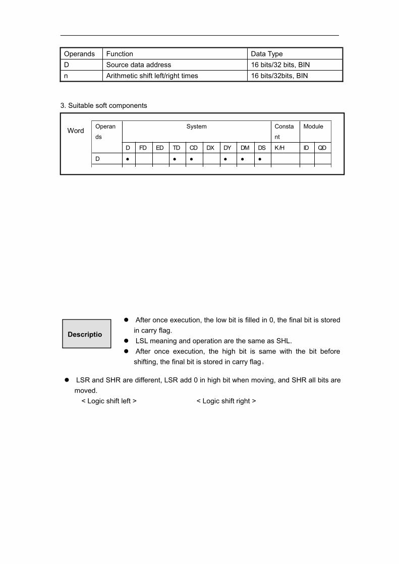
Operands Function Data TypeD Source data address 16 bits/32 bits, BINn Arithmetic shift left/right times 16 bits/32bits, BIN
3. Suitable soft components
LSR and SHR are different, LSR add 0 in high bit when moving, and SHR all bits aremoved.< Logic shift left > < Logic shift right >
Operan
ds
System Consta
nt
Module
D FD ED TD CD DX DY DM DS K/H ID QD
D ● ● ● ● ● ●
n ●
Word
After once execution, the low bit is filled in 0, the final bit is storedin carry flag.
LSL meaning and operation are the same as SHL. After once execution, the high bit is same with the bit before
shifting, the final bit is stored in carry flag。
Descriptio
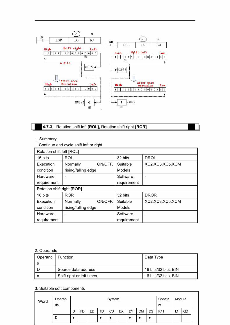
4-7-3.Rotation shift left [ROL], Rotation shift right [ROR]
1. SummaryContinue and cycle shift left or rightRotation shift left [ROL]16 bits ROL 32 bits DROLExecutioncondition
Normally ON/OFF,rising/falling edge
SuitableModels
XC2.XC3.XC5.XCM
Hardwarerequirement
- Softwarerequirement
-
Rotation shift right [ROR]16 bits ROR 32 bits DRORExecutioncondition
Normally ON/OFF,rising/falling edge
SuitableModels
XC2.XC3.XC5.XCM
Hardwarerequirement
- Softwarerequirement
-
2. OperandsOperands
Function Data Type
D Source data address 16 bits/32 bits, BINn Shift right or left times 16 bits/32 bits, BIN
3. Suitable soft components
Operan
ds
System Consta
nt
Module
D FD ED TD CD DX DY DM DS K/H ID QD
D ● ● ● ● ● ●
n ●
Word

< Rotation shift left > < Rotation shift right >
4-7-4.Bit shift left [SFTL]
1. SummaryBit shift leftBit shift left [SFTL]16 bits SFTL 32 bits DSFTLExecutioncondition
Normally ON/OFF,rising/falling edge
SuitableModels
XC2.XC3.XC5.XCM
Hardwarerequirement
- Softwarerequirement
-
2. OperandsOperands
Function Types
S Source soft element head address bitD Target soft element head address bitn1 Source data quantity 16 bits /32 bits, BIN
The bit format of the destination device is rotated n bit places tothe left on every operation of the instruction.
Descriptio
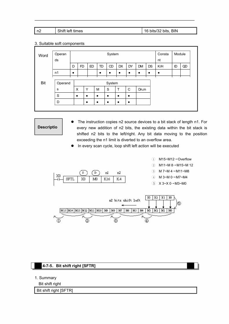
n2 Shift left times 16 bits/32 bits, BIN
3. Suitable soft components
4-7-5.Bit shift right [SFTR]
1. SummaryBit shift rightBit shift right [SFTR]
Word Operan
ds
System Consta
nt
Module
D FD ED TD CD DX DY DM DS K/H ID QD
n1 ● ● ● ● ● ● ● ●
n2 ● ● ● ● ● ● ● ●Operand
s
System
X Y M S T C Dn..m
S ● ● ● ● ● ●
D ● ● ● ● ●
Bit
The instruction copies n2 source devices to a bit stack of length n1. Forevery new addition of n2 bits, the existing data within the bit stack isshifted n2 bits to the left/right. Any bit data moving to the positionexceeding the n1 limit is diverted to an overflow area.
In every scan cycle, loop shift left action will be executed
Descriptio
1 M15~M12→Overflow
2 M11~M 8→M15~M 12
3 M 7~M 4→M11~M8
4 M 3~M 0→M7~M4
5 X 3~X 0→M3~M0

16 bits SFTR 32 bits DSFTRExecutioncondition
rising/falling edge SuitableModels
XC2.XC3.XC5.XCM
Hardwarerequirement
- Softwarerequirement
-
2. OperandsOperands
Function Data Type
S Source soft element head address bitD Target soft element head address bitn1 Source data quantity 16 bits/32 bits, BINn2 Shift right times 16 bits/32 bits, BIN
3. Suitable soft components
Operan
ds
System Consta
nt
Module
D FD ED TD CD DX DY DM DS K/H ID QD
n1 ● ● ● ● ● ● ● ●
n2 ● ● ● ● ● ● ● ●
Word
Bit
The instruction copies n2 source devices to a bit stack of length n1.For every new addition of n2 bits, the existing data within the bitstack is shifted n2 bits to the left/right. Any bit data moving to theposition exceeding the n1 limit is diverted to an overflow area.
In every scan cycle, loop shift right action will be executed
Descriptio
Operand
s
System
X Y M S T C Dn..m
S ● ● ● ● ● ●
D ● ● ● ● ●
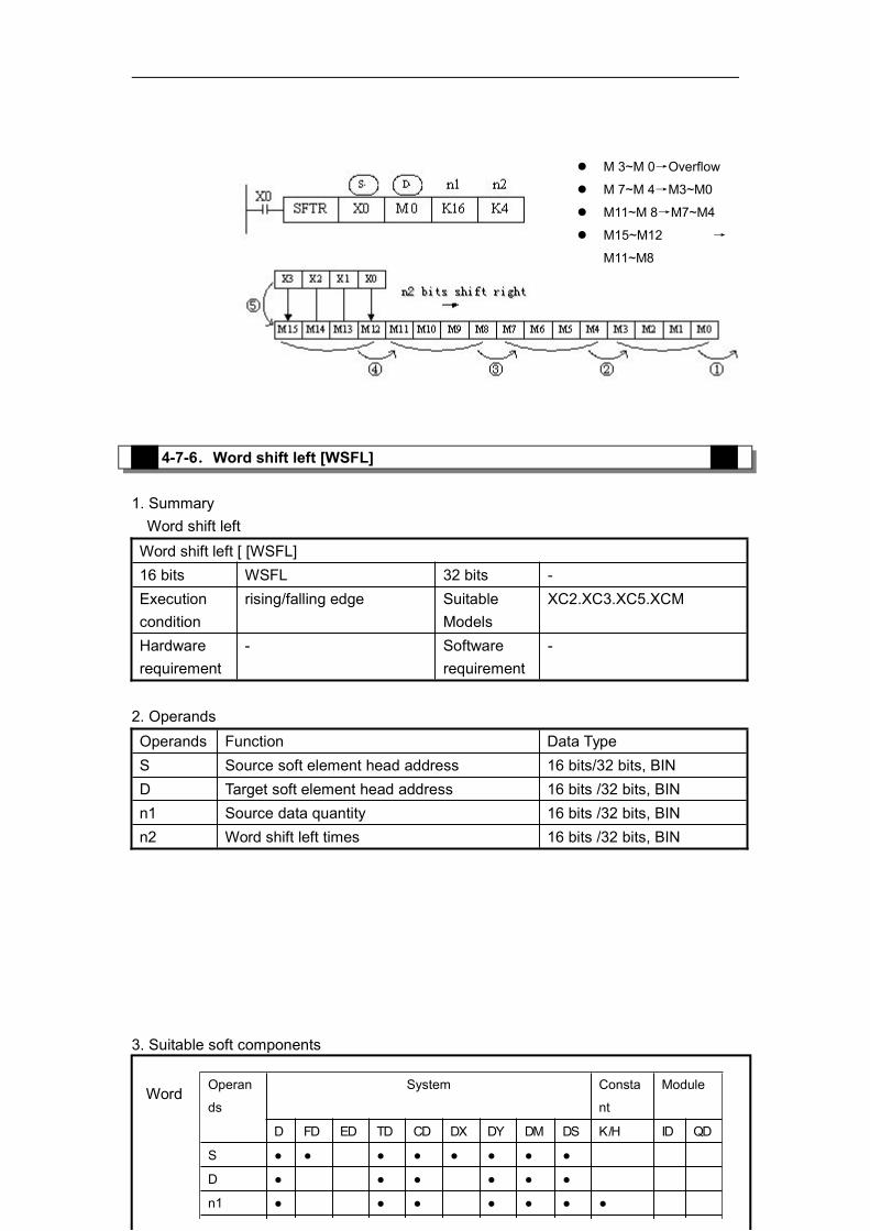
4-7-6.Word shift left [WSFL]
1. SummaryWord shift leftWord shift left [ [WSFL]16 bits WSFL 32 bits -Executioncondition
rising/falling edge SuitableModels
XC2.XC3.XC5.XCM
Hardwarerequirement
- Softwarerequirement
-
2. OperandsOperands Function Data TypeS Source soft element head address 16 bits/32 bits, BIND Target soft element head address 16 bits /32 bits, BINn1 Source data quantity 16 bits /32 bits, BINn2 Word shift left times 16 bits /32 bits, BIN
3. Suitable soft components
M 3~M 0→Overflow
M 7~M 4→M3~M0
M11~M 8→M7~M4
M15~M12 →
M11~M8
Operan
ds
System Consta
nt
Module
D FD ED TD CD DX DY DM DS K/H ID QD
S ● ● ● ● ● ● ● ●
D ● ● ● ● ● ●
n1 ● ● ● ● ● ● ●
n2 ● ● ● ● ● ● ●
Word

n2 word shift left
4-7-7.Word shift right [WSFR]
1. SummaryWord shift rightWord shift right [WSFR]16 bits WSFR 32 bits -Executioncondition
rising/falling edge SuitableModels
XC2.XC3.XC5.XCM
Hardwarerequirement
- Softwarerequirement
-
2. OperandsOperands Function Data TypeS Source soft element head address 16 bits/32 bits, BIND Target soft element head address 16 bits/32 bits, BIN
Descriptio The instruction copies n2 source devices to a word stack of lengthn1. For each addition of n2 words, the existing data within theword stack is shifted n2 words to the left. Any word data moving toa position exceeding the n1 limit is diverted to an overflow area.
In every scan cycle, loop shift left action will be executed.
1 D25~D22→Overflow
2 D21~D18→D25~D22
3 D17~D14→D21~D18
4 D13~D10→D17~D14
5 D 3~D 0→D13~D10

n2字右移
n1 Source data quantity 16 bits/32 bits, BINn2 Shift right times 16 bits/32 bits, BIN
3. Suitable soft components
4-8.Data Convert
Mnemonic Function ChapterWTD Single word integer converts to
double word integer4-8-1
FLT 16 bits integer converts to floatpoint
4-8-2
DFLT 32 bits integer converts to floatpoint
4-8-2
FLTD 64 bits integer converts to floatpoint
4-8-2
INT Float point converts to integer 4-8-3BIN BCD convert to binary 4-8-4
Operan
ds
System Consta
nt
Module
D FD ED TD CD DX DY DM DS K/H ID QD
S ● ● ● ● ● ● ● ●
D ● ● ● ● ● ●
n1 ● ● ● ● ● ● ●
n2 ● ● ● ● ● ● ●
Word
Descriptio The instruction copies n2 source devices to a word stack of length
n1. For each addition of n2 words, the existing data within theword stack is shifted n2 words to the right. Any word data movingto a position exceeding the n1 limit is diverted to an overflow area.
D13~D10→Overflow
D17~D14 →
D13~D10
D21~D18 →
D17~D14
In every scan cycle, loop shift right action will be executed
BCD Binary converts to BCD 4-8-5ASCI Hex. converts to ASCII 4-8-6HEX ASCII converts to Hex. 4-8-7DECO Coding 4-8-8ENCO High bit coding 4-8-9ENCOL Low bit coding 4-8-10
4-8-1.Single word integer converts to double word integer [WTD]
1. SummarySingle word integer converts to double word integer [WTD]16 bits WTD 32 bits -Executioncondition
Normally ON/OFF,rising/falling edge
SuitableModels
XC2.XC3.XC5.XCM
Hardwarerequirement
- Softwarerequirement
-
2. OperandsOperands
Function Data Type
S Source soft element address 16 bits, BIND Target soft element address 32 bits, BIN
3. Suitable soft components
Operan
ds
System Consta
nt
Module
D FD ED TD CD DX DY DM DS K/H ID QD
S ● ● ● ● ● ● ● ●
D ● ● ● ● ● ●
Word
Descriptio

WTD D0 D10X0
S· D·
High bits Low bits
D11 D10
0 or 1 D0
4-8-2.16 bits integer converts to float point [FLT]
1. Summary16 bits integer converts to float point [FLT]16 bits FLT 32 bits DFLT 64 bits FLTDExecutioncondition
Normally ON/OFF,rising/falling edge
SuitableModels
XC2.XC3.XC5.XCM
Hardwarerequirement
- Softwarerequirement
-
2. OperandsOperands Function Data TypeS Source soft element address 16 bits/32 bits/64 bits, BIND Target soft element address 32 bits/64 bits, BIN
3. Suitable soft components
(D0) → (D11,D10)Single Word Double
When single word D0 is positive integer, after executing thisinstruction, the high bit of double word D10 is 0.
When single word D0 is negative integer, after executing thisinstruction, the high bit of double word D10 is 1.
Operan
ds
System Consta
nt
Module
D FD ED TD CD DX DY DM DS K/H ID QD
S ● ● ●
D ●
Word
Descriptio
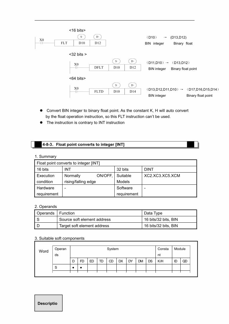
<16 bits>
<32 bits >
DFLT D10 D12
S· D·X0
<64 bits>
FLTD D10 D14
S· D·X0
4-8-3.Float point converts to integer [INT]
1. SummaryFloat point converts to integer [INT]16 bits INT 32 bits DINTExecutioncondition
Normally ON/OFF,rising/falling edge
SuitableModels
XC2.XC3.XC5.XCM
Hardwarerequirement
- Softwarerequirement
-
2. OperandsOperands Function Data TypeS Source soft element address 16 bits/32 bits, BIND Target soft element address 16 bits/32 bits, BIN
3. Suitable soft components
(D10) → (D13,D12)
BIN integer Binary float
point
FLT D10 D12
S· D·X0
(D11,D10)→ (D13,D12)
BIN integer Binary float point
(D13,D12,D11,D10)→ (D17,D16,D15,D14)
BIN integer Binary float point
Convert BIN integer to binary float point. As the constant K, H will auto convertby the float operation instruction, so this FLT instruction can’t be used.
The instruction is contrary to INT instruction
Operan
ds
System Consta
nt
Module
D FD ED TD CD DX DY DM DS K/H ID QD
S ● ●
D ●
Word
Descriptio
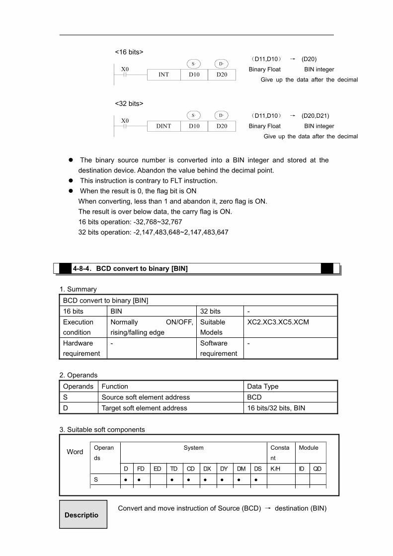
<16 bits>
INT D10 D20
S· D·X0
<32 bits>
DINT D10 D20
S· D·X0
4-8-4.BCD convert to binary [BIN]
1. SummaryBCD convert to binary [BIN]16 bits BIN 32 bits -Executioncondition
Normally ON/OFF,rising/falling edge
SuitableModels
XC2.XC3.XC5.XCM
Hardwarerequirement
- Softwarerequirement
-
2. OperandsOperands Function Data TypeS Source soft element address BCDD Target soft element address 16 bits/32 bits, BIN
3. Suitable soft components
(D11,D10) → (D20)
Binary Float BIN integer
Give up the data after the decimal
(D11,D10) → (D20,D21)
Binary Float BIN integer
Give up the data after the decimal
The binary source number is converted into a BIN integer and stored at thedestination device. Abandon the value behind the decimal point.
This instruction is contrary to FLT instruction. When the result is 0, the flag bit is ON
When converting, less than 1 and abandon it, zero flag is ON.The result is over below data, the carry flag is ON.16 bits operation: -32,768~32,76732 bits operation: -2,147,483,648~2,147,483,647
Operan
ds
System Consta
nt
Module
D FD ED TD CD DX DY DM DS K/H ID QD
S ● ● ● ● ● ● ● ●
D ● ● ● ● ● ●
Word
DescriptioConvert and move instruction of Source (BCD) → destination (BIN)
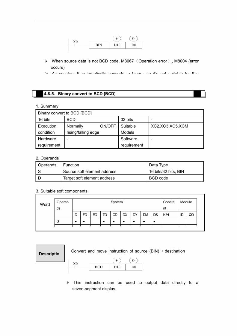
BIN D10 D0
S· D·X0
4-8-5.Binary convert to BCD [BCD]
1. SummaryBinary convert to BCD [BCD]16 bits BCD 32 bits -Executioncondition
Normally ON/OFF,rising/falling edge
SuitableModels
XC2.XC3.XC5.XCM
Hardwarerequirement
- Softwarerequirement
-
2. OperandsOperands Function Data TypeS Source soft element address 16 bits/32 bits, BIND Target soft element address BCD code
3. Suitable soft components
BCD D10 D0
S· D·X0
When source data is not BCD code, M8067(Operation error), M8004 (erroroccurs)
As constant K automatically converts to binary, so it’s not suitable for this
Operan
ds
System Consta
nt
Module
D FD ED TD CD DX DY DM DS K/H ID QD
S ● ● ● ● ● ● ● ●
D ● ● ● ● ● ●
Word
Descriptio Convert and move instruction of source (BIN)→ destination
This instruction can be used to output data directly to aseven-segment display.

4-8-6.Hex. Converts to ASCII [ASCI]
1. SummaryHex. convert to ASCII [ASCI]16 bits ASCI 32 bits -Executioncondition
Normally ON/OFF,rising/falling edge
SuitableModels
XC2.XC3.XC5.XCM
Hardwarerequirement
- Softwarerequirement
-
2. OperandsOperands Function Data TypeS Source soft element address 2 bits, HEXD Target soft element address ASCII coden Transform character quantity 16 bits, BIN
3. Suitable soft components
ASCI D100 D200 K4
S· D· nX0
Operan
ds
System Consta
nt
Module
D FD ED TD CD DX DY DM DS K/H ID QD
S ● ● ● ● ● ● ● ●
D ● ● ● ● ● ●
n ● ● ● ● ● ● ●
Word
Descriptio
D·S· Convert each bit of source’s (S) hex format data to be ASCII code, move separatelyto the high 8 bits and low 8 bits of destination (D). The convert alphanumericnumber is assigned with n.is low 8 bits, high 8 bits, store ASCII data.D·

The convert result is this
4-8-7.ASCII converts to hex. [HEX]
1. SummaryASCII converts to Hex. [HEX]16 bits HEX 32 bits -Executioncondition
Normally ON/OFF,rising/falling edge
SuitableModels
XC2.XC3.XC5.XCM
Hardwarerequirement
- Softwarerequirement
-
2. OperandsOperands Function Date typeS Source soft element address ASCIID Target soft element address 2 bits, HEXn Character quantity 16 bits, BIN
3. Suitable soft components
nD
K1 K2 K3 K4 K5 K6 K7 K8 K9
D200down
[C] [B] [A] [0] [4] [3] [2] [1] [8]
D200 up [C] [B] [A] [0] [4] [3] [2] [1]D201down
[C] [B] [A] [0] [4] [3] [2]
D201 up [C] [B] [A] [0] [4] [3]D202down
[C] [B] [A] [0] [4]
D202 up [C] [B] [A] [0]D203down
[C] [B] [A]
D203 up [C] [B]D204down
[C]
Assign startdevice:(D100)=0ABCH(D101)=1234H(D102)=5678H[0]=30H [1] =31H[5]=35H [A] =41H[2]=32H [6] =36H[B]=42H [3] =33H[7]=37H [C]=43H[4]=34H [8] =38H
Operan
ds
System Consta
nt
Module
D FD ED TD CD DX DY DM DS K/H ID QD
S ● ● ● ● ● ● ● ●
D ● ● ● ● ● ●
n ●
Word
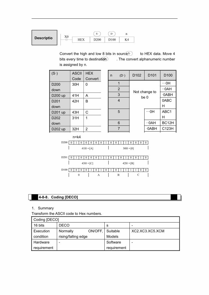
HEX D200 D100 K4
S· D· nX0
The convert of the upward program is the following:
时
n=k40 1 0 0 0 0 0 1 0 0 1 1 0 0 0 0D200
41H→[A] 30H→[0]
0 1 0 0 0 0 1 1 0 1 0 1 0 0 1 0D201
43H→[C] 42H→[B]
0 0 0 0 1 0 1 0 1 0 1 1 1 1 0 0D100
0 A B C
4-8-8.Coding [DECO]
1. SummaryTransform the ASCII code to Hex numbers.Coding [DECO]16 bits DECO s -Executioncondition
Normally ON/OFF,rising/falling edge
SuitableModels
XC2.XC3.XC5.XCM
Hardwarerequirement
- Softwarerequirement
-
Descriptio
Convert the high and low 8 bits in source to HEX data. Move 4bits every time to destination . The convert alphanumeric numberis assigned by n.
S·
D·
(S·) ASCIICode
HEXConvert
D200down
30H 0
D200 up 41H AD201down
42H B
D201 up 43H CD202down
31H 1
D202 up 32H 2D203 33H 3
n (D·) D102 D101 D100
1
Not change tobe 0
···0H2 ··0AH3 ·0ABH4 0ABC
H5 ···0H ABC1
H6 ··0AH BC12H7 ·0ABH C123H8 0ABC 1234H

③
② ①
2. OperandsOperands Function Data TypeS Source soft element address ASCIID Target soft element address 2 bits HEXn The coding soft element quantity 16bits, BIN
3.Suitable soft components
< When is bit unit > n≤16
DX0DECO M10 K3X10
nS· D·
0 1 1
0 0 0 1 0 0 0
X002 X001 X000
M17 M16 M15 M14 M13 M12 M11 M10
7 6 5 4 2 1 0
4
0
< When is word device > n≤4
D0DECO D1 K3X0
nS· D·
Operan
ds
System Consta
nt
Module
D FD ED TD CD DX DY DM DS K/H ID QD
S ● ● ● ● ● ● ● ●
n ●
Word
Operand
s
System
X Y M S T C Dn.m
D ● ● ● ● ● ●
Bit
Descriptio D·
The source address is 1+2=3,so starts from M10, the number 3bit (M13) is 1. If the source is all 0, M10 is 1.
When n=0, no operation, beyond n=0~16, don’t execute theinstruction.
When n=16, if coding command is soft unit, it’s point is2^16=65536。
When drive input is OFF, instructions are not executed, the
D·
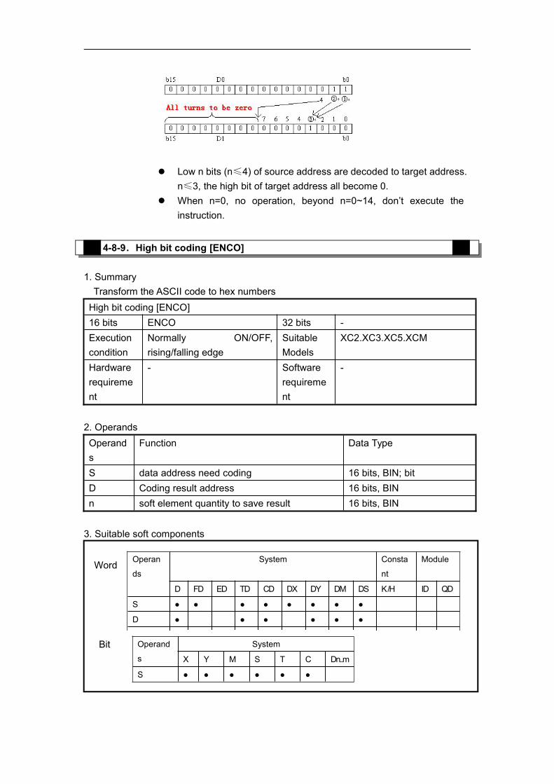
全部转化为 0③
①②
4-8-9.High bit coding [ENCO]
1. SummaryTransform the ASCII code to hex numbersHigh bit coding [ENCO]16 bits ENCO 32 bits -Executioncondition
Normally ON/OFF,rising/falling edge
SuitableModels
XC2.XC3.XC5.XCM
Hardwarerequirement
- Softwarerequirement
-
2. OperandsOperands
Function Data Type
S data address need coding 16 bits, BIN; bitD Coding result address 16 bits, BINn soft element quantity to save result 16 bits, BIN
3. Suitable soft components
Low n bits (n≤4) of source address are decoded to target address.n≤3, the high bit of target address all become 0.
When n=0, no operation, beyond n=0~14, don’t execute theinstruction.
Operan
ds
System Consta
nt
Module
D FD ED TD CD DX DY DM DS K/H ID QD
S ● ● ● ● ● ● ● ●
D ● ● ● ● ● ●
n ●
Word
Operand
s
System
X Y M S T C Dn..m
S ● ● ● ● ● ●
Bit
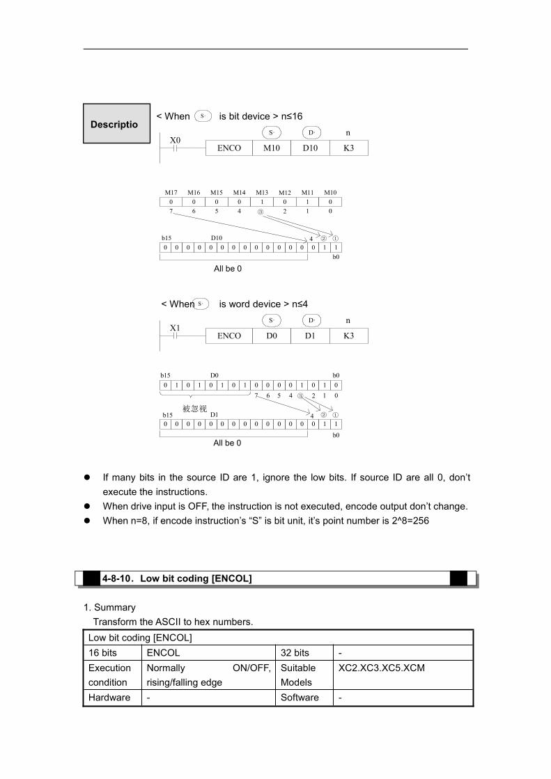
All be 0
② ①
③
被忽视
All be 0
①②
③
< When is bit device > n≤16
M10ENCO D10 K3X0
nS· D·
0 0 0 1 0 1 0M17 M16 M15 M14 M13 M12 M11 M10
7 6 5 4 2 1 00
0 0 0 0 0 0 0 0 0 0 0 0 0 0 1 1D10b15
b0
4
< When is word device > n≤4
D0ENCO D1 K3X1
nS· D·
0 1 0 1 0 1 0 1 0 0 0 0 1 0 1 0
0 0 0 0 0 0 0 0 0 0 0 0 0 0 1 1
7 6 5 4 2 1 0
D0
D1b15
b15 b0
b0
4
If many bits in the source ID are 1, ignore the low bits. If source ID are all 0, don’texecute the instructions.
When drive input is OFF, the instruction is not executed, encode output don’t change. When n=8, if encode instruction’s “S” is bit unit, it’s point number is 2^8=256
4-8-10.Low bit coding [ENCOL]
1. SummaryTransform the ASCII to hex numbers.Low bit coding [ENCOL]16 bits ENCOL 32 bits -Executioncondition
Normally ON/OFF,rising/falling edge
SuitableModels
XC2.XC3.XC5.XCM
Hardware - Software -
DescriptioS·
S·
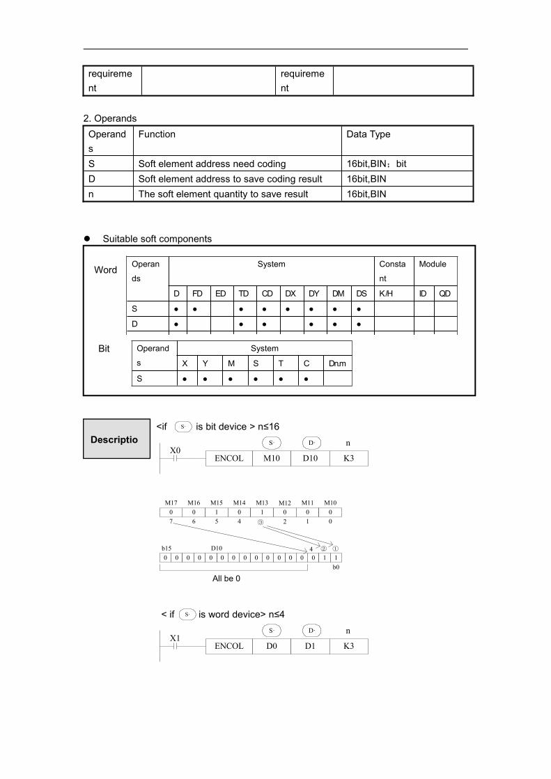
All be 0
② ①
③
requirement
requirement
2. OperandsOperands
Function Data Type
S Soft element address need coding 16bit,BIN;bitD Soft element address to save coding result 16bit,BINn The soft element quantity to save result 16bit,BIN
Suitable soft components
<if is bit device > n≤16
M10ENCOL D10 K3X0
nS· D·
0 1 0 1 0 0 0M17 M16 M15 M14 M13 M12 M11 M10
7 6 5 4 2 1 00
0 0 0 0 0 0 0 0 0 0 0 0 0 0 1 1D10b15
b0
4
< if is word device> n≤4
D0ENCOL D1 K3X1
nS· D·
Operan
ds
System Consta
nt
Module
D FD ED TD CD DX DY DM DS K/H ID QD
S ● ● ● ● ● ● ● ●
D ● ● ● ● ● ●
n ●
Word
Operand
s
System
X Y M S T C Dn.m
S ● ● ● ● ● ●
Bit
DescriptioS·
S·
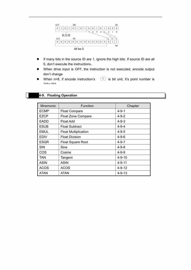
被忽视
All be 0
①②
③
0 1 0 1 0 1 0 1 0 0 1 0 1 0 0 0
0 0 0 0 0 0 0 0 0 0 0 0 0 0 1 1
7 6 5 4 2 1 0
D0
D1b15
b15 b0
b0
4
4-9.Floating Operation
Mnemonic Function ChapterECMP Float Compare 4-9-1EZCP Float Zone Compare 4-9-2EADD Float Add 4-9-3ESUB Float Subtract 4-9-4EMUL Float Multiplication 4-9-5EDIV Float Division 4-9-6ESQR Float Square Root 4-9-7SIN Sine 4-9-8COS Cosine 4-9-9TAN Tangent 4-9-10ASIN ASIN 4-9-11ACOS ACOS 4-9-12ATAN ATAN 4-9-13
If many bits in the source ID are 1, ignore the high bits. If source ID are all0, don’t execute the instructions。
When drive input is OFF, the instruction is not executed, encode outputdon’t change
When n=8, if encode instruction’s is bit unit, it’s point number is2^8=256
S·
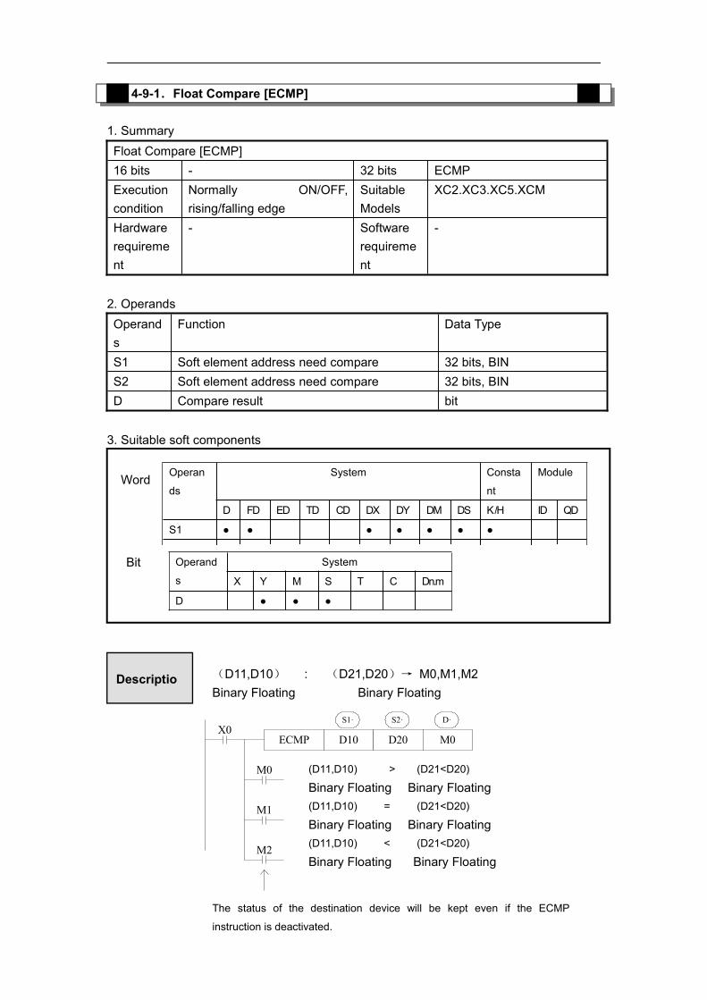
4-9-1.Float Compare [ECMP]
1. SummaryFloat Compare [ECMP]16 bits - 32 bits ECMPExecutioncondition
Normally ON/OFF,rising/falling edge
SuitableModels
XC2.XC3.XC5.XCM
Hardwarerequirement
- Softwarerequirement
-
2. OperandsOperands
Function Data Type
S1 Soft element address need compare 32 bits, BINS2 Soft element address need compare 32 bits, BIND Compare result bit
3. Suitable soft components
ECMP D10 D20 M0
M0
M1
M2
X0D·S1· S2·
Operan
ds
System Consta
nt
Module
D FD ED TD CD DX DY DM DS K/H ID QD
S1 ● ● ● ● ● ● ●
S2 ● ● ● ● ● ● ●
Word
Operand
s
System
X Y M S T C Dn.m
D ● ● ●
Bit
(D11,D10) : (D21,D20)→ M0,M1,M2Binary Floating Binary Floating
Descriptio
(D11,D10) > (D21<D20)
Binary Floating Binary Floating(D11,D10) = (D21<D20)
Binary Floating Binary Floating(D11,D10) < (D21<D20)
Binary Floating Binary Floating
The status of the destination device will be kept even if the ECMP
instruction is deactivated.

ECMP K500 D100 M10X0
4-9-2.Float Zone Compare [EZCP]
1. SummaryFloat Zone Compare [EZCP]16 bits - 32 bits EZCPExecutioncondition
Normally ON/OFF,rising/falling edge
SuitableModels
XC2.XC3.XC5.XCM
Hardwarerequirement
- Softwarerequirement
-
2. OperandsOperands
Function Data Type
S1 Soft element address need compare 32 bits, BINS2 Upper limit of compare data 32 bits, BINS3 Lower limit of compare data 32 bits, BIND The compare result soft element address bit
3. Suitable soft components
The binary float data of S1 is compared to S2. The result is indicated by 3 bitdevices specified with the head address entered as D
If a constant K or H used as source data, the value is converted to floatingpoint before the addition operation.
(K500) : (D101,D100)→M10,M11,M12
Binary converts Binary floating
to floating
Operan
ds
System Consta
nt
Module
D FD ED TD CD DX DY DM DS K/H ID QD
S1 ● ● ● ● ● ● ●
S2 ● ● ● ● ● ● ●
S3 ● ● ● ● ● ● ●
Word
Operand
s
System
X Y M S T C Dn..m
D ● ● ●
Bit

Compare a float range with a float value...
EZCP D10 D20 D0
M3
M4
M5
X0S1· S2·
M3
S3· D·
EZCP K10 K2800 D5 M0X0
4-9-3.Float Add [EADD]
1. SummaryFloat Add [EADD]16 bits - 32 bits EADDExecutioncondition
Normally ON/OFF,rising/falling edge
SuitableModels
XC2.XC3.XC5.XCM
Hardwarerequirement
- Softwarerequirement
-
2. Operands
Descriptio
(D1,D0) < (D11,D10) ON
Binary Floating Binary Floating
(D11,D10) ≤ (D1,D0 ) ≤(D21,D20) ON
Binary Floating Binary Floating Binary Floating
(D1,D0) > (D21, D20) ON
Binary Floating Binary Floating
The status of the destination device will be kept even if the EZCP
instruction is deactivated.
The data of S1 is compared to the data of S2. The result isindicated by 3 bit devices specified with the head address enteredas D.
If a constant K or H used as source data, the value is converted to
(K10)∶ [D6,D5]∶ (K2800)→ M0,M1,M2
Binary converts Binary Floating Binary converts
to Floating to Floating
Please set S1<S2, when S2>S1, see S2 as the same with S1 andcompare them
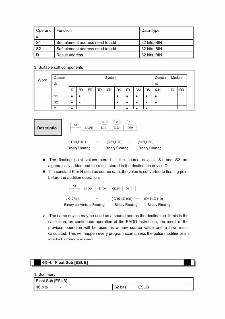
Operands
Function Data Type
S1 Soft element address need to add 32 bits, BINS2 Soft element address need to add 32 bits, BIND Result address 32 bits, BIN
3. Suitable soft components
EADD D10 D20 D50
S1· S2· D·X0
EADD D100 K1234 D110X1
4-9-4.Float Sub [ESUB]
1. SummaryFloat Sub [ESUB]16 bits - 32 bits ESUB
Operan
ds
System Consta
nt
Module
D FD ED TD CD DX DY DM DS K/H ID QD
S1 ● ● ● ● ● ● ●
S2 ● ● ● ● ● ● ●
D ● ● ● ●
Word
Descriptio
(D11,D10) + (D21,D20) → (D51,D50)
Binary Floating Binary Floating Binary Floating
The floating point values stored in the source devices S1 and S2 arealgebraically added and the result stored in the destination device D.
If a constant K or H used as source data, the value is converted to floating pointbefore the addition operation.
(K1234) + ( D101,D100) → (D111,D110)
Binary converts to Floating Binary Floating Binary Floating
The same device may be used as a source and as the destination. If this is thecase then, on continuous operation of the EADD instruction, the result of theprevious operation will be used as a new source value and a new resultcalculated. This will happen every program scan unless the pulse modifier or aninterlock program is used.

Executioncondition
Normally ON/OFF,rising/falling edge
SuitableModels
XC2.XC3.XC5.XCM
Hardwarerequirement
- Softwarerequirement
-
2. OperandsOperands
Function Data Type
S1 Soft element address need to subtract 32 bits, BINS2 Soft element address need to subtract 32 bits, BIND Result address 32 bits, BIN
3. Suitable soft components
ESUB D10 D20 D50
S1· S2· D·X0
ESUB D100K1234 D110X1
Operan
ds
System Consta
nt
Module
D FD ED TD CD DX DY DM DS K/H ID QD
S1 ● ● ● ● ● ● ●
S2 ● ● ● ● ● ● ●
D ● ● ● ●
Word
Descriptio
(D11,D10) - (D21,D20) → (D51,D50)
Binary Floating Binary Floating Binary Floating
The floating point value of S2 is subtracted from the floating point value of S1 andthe result stored in destination device D.
If a constant K or H used as source data, the value is converted to floating pointbefore the addition operation。
(K1234) - (D101,D100) → (D111,D110)
Binary converts to Floating Binary Floating Binary Floating
The same device may be used as a source and as the destination. If this is thecase then, on continuous operation of the EADD instruction, the result of theprevious operation will be used as a new source value and a new result calculated.This will happen every program scan unless the pulse modifier or an interlock
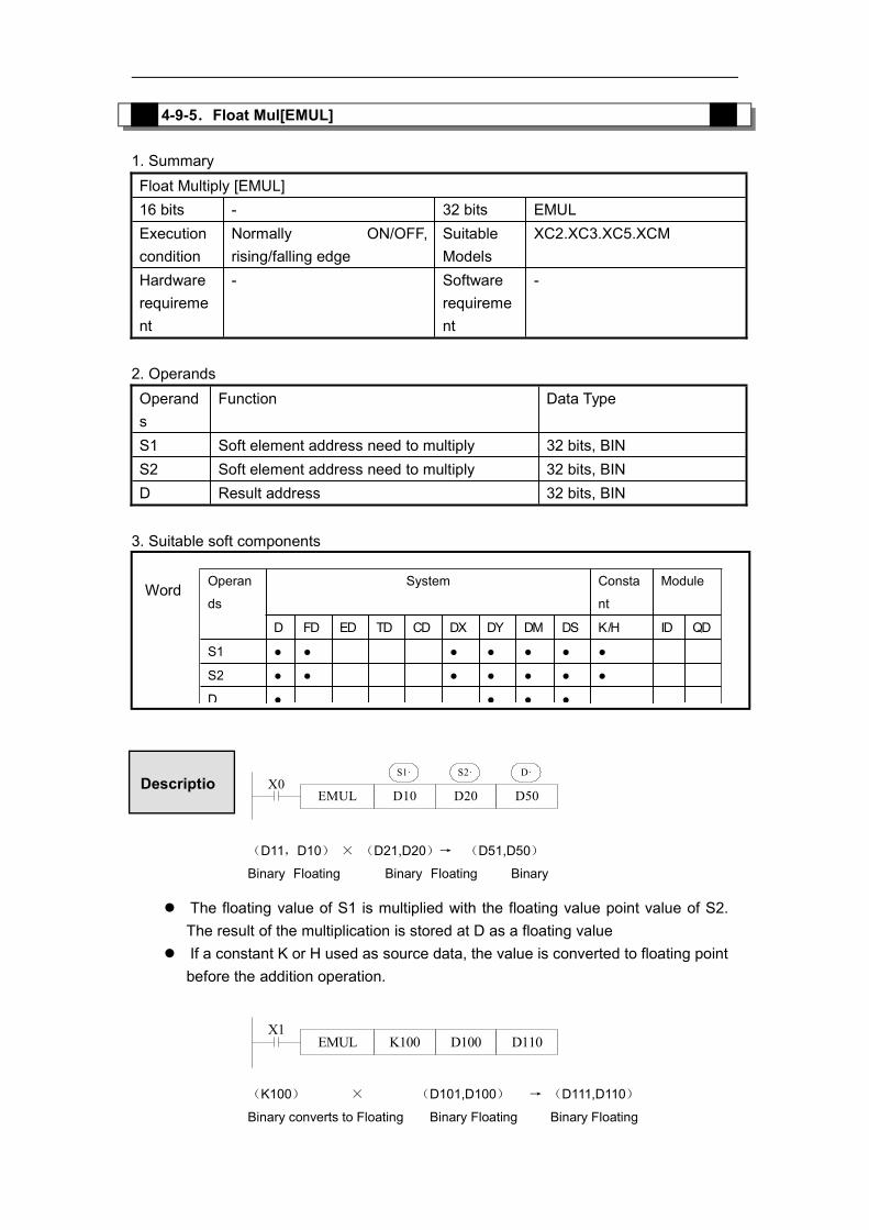
4-9-5.Float Mul[EMUL]
1. SummaryFloat Multiply [EMUL]16 bits - 32 bits EMULExecutioncondition
Normally ON/OFF,rising/falling edge
SuitableModels
XC2.XC3.XC5.XCM
Hardwarerequirement
- Softwarerequirement
-
2. OperandsOperands
Function Data Type
S1 Soft element address need to multiply 32 bits, BINS2 Soft element address need to multiply 32 bits, BIND Result address 32 bits, BIN
3. Suitable soft components
EMUL D10 D20 D50
S1· S2· D·X0
EMUL D100K100 D110X1
Operan
ds
System Consta
nt
Module
D FD ED TD CD DX DY DM DS K/H ID QD
S1 ● ● ● ● ● ● ●
S2 ● ● ● ● ● ● ●
D ● ● ● ●
Word
Descriptio
(D11,D10) × (D21,D20)→ (D51,D50)
Binary Floating Binary Floating Binary
The floating value of S1 is multiplied with the floating value point value of S2.The result of the multiplication is stored at D as a floating value
If a constant K or H used as source data, the value is converted to floating pointbefore the addition operation.
(K100) × (D101,D100) → (D111,D110)
Binary converts to Floating Binary Floating Binary Floating

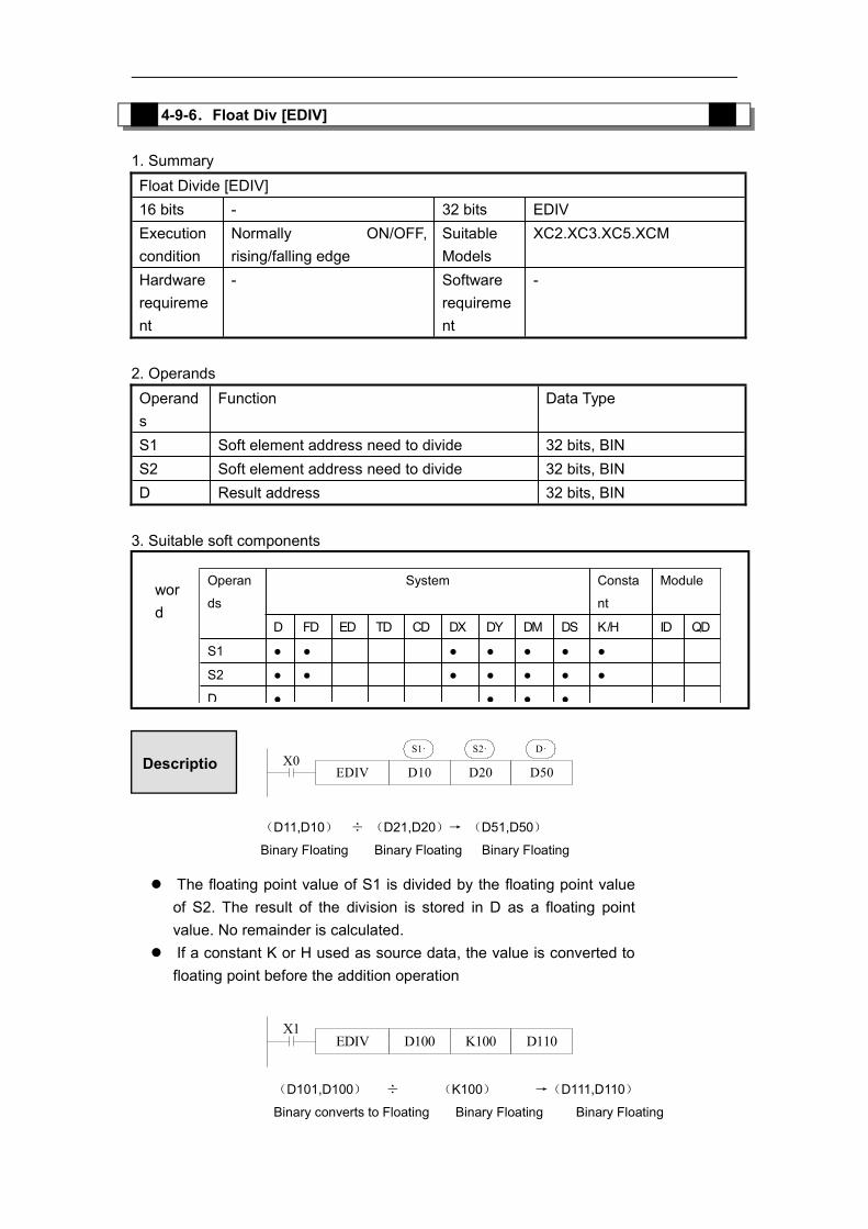
4-9-6.Float Div [EDIV]
1. SummaryFloat Divide [EDIV]16 bits - 32 bits EDIVExecutioncondition
Normally ON/OFF,rising/falling edge
SuitableModels
XC2.XC3.XC5.XCM
Hardwarerequirement
- Softwarerequirement
-
2. OperandsOperands
Function Data Type
S1 Soft element address need to divide 32 bits, BINS2 Soft element address need to divide 32 bits, BIND Result address 32 bits, BIN
3. Suitable soft components
EDIV D10 D20 D50
S1· S2· D·X0
EDIV D100 K100 D110X1
Operan
ds
System Consta
nt
Module
D FD ED TD CD DX DY DM DS K/H ID QD
S1 ● ● ● ● ● ● ●
S2 ● ● ● ● ● ● ●
D ● ● ● ●
word
Descriptio
(D11,D10) ÷ (D21,D20)→ (D51,D50)
Binary Floating Binary Floating Binary Floating
The floating point value of S1 is divided by the floating point valueof S2. The result of the division is stored in D as a floating pointvalue. No remainder is calculated.
If a constant K or H used as source data, the value is converted tofloating point before the addition operation
(D101,D100) ÷ (K100) →(D111,D110)
Binary converts to Floating Binary Floating Binary Floating

If S2 is 0, the calculate is error, the instruction can not work
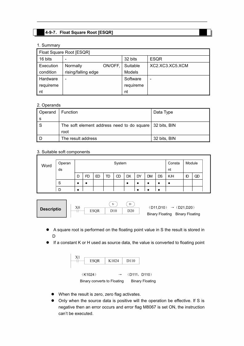
4-9-7.Float Square Root [ESQR]
1. SummaryFloat Square Root [ESQR]16 bits - 32 bits ESQRExecutioncondition
Normally ON/OFF,rising/falling edge
SuitableModels
XC2.XC3.XC5.XCM
Hardwarerequirement
- Softwarerequirement
-
2. OperandsOperands
Function Data Type
S The soft element address need to do squareroot
32 bits, BIN
D The result address 32 bits, BIN
3. Suitable soft components
ESQR D10 D20X0
S· D·
ESQR K1024 D110X1
Operan
ds
System Consta
nt
Module
D FD ED TD CD DX DY DM DS K/H ID QD
S ● ● ● ● ● ● ●
D ● ● ● ●
Word
(D11,D10) →(D21,D20)
Binary Floating Binary FloatingDescriptio
A square root is performed on the floating point value in S the result is stored inD
If a constant K or H used as source data, the value is converted to floating point
(K1024) → (D111,D110)
Binary converts to Floating Binary Floating
When the result is zero, zero flag activates. Only when the source data is positive will the operation be effective. If S is
negative then an error occurs and error flag M8067 is set ON, the instructioncan’t be executed.

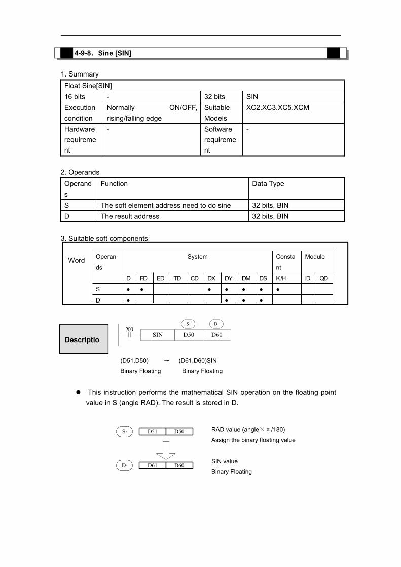
4-9-8.Sine [SIN]
1. SummaryFloat Sine[SIN]16 bits - 32 bits SINExecutioncondition
Normally ON/OFF,rising/falling edge
SuitableModels
XC2.XC3.XC5.XCM
Hardwarerequirement
- Softwarerequirement
-
2. OperandsOperands
Function Data Type
S The soft element address need to do sine 32 bits, BIND The result address 32 bits, BIN
3. Suitable soft components
SIN D50 D60X0
S· D·
D51 D50
D61 D60
S·
D·
Operan
ds
System Consta
nt
Module
D FD ED TD CD DX DY DM DS K/H ID QD
S ● ● ● ● ● ● ●
D ● ● ● ●
Word
Descriptio
(D51,D50) → (D61,D60)SIN
Binary Floating Binary Floating
This instruction performs the mathematical SIN operation on the floating pointvalue in S (angle RAD). The result is stored in D.
RAD value (angle×π/180)
Assign the binary floating value
SIN value
Binary Floating


4-9-9.Cosine [SIN]
1. SummaryFloat Cosine[COS]16 bits - 32 bits COSExecutioncondition
Normally ON/OFF,rising/falling edge
SuitableModels
XC2.XC3.XC5.XCM
Hardwarerequirement
- Softwarerequirement
-
2. OperandsOperands
Function Data Type
S Soft element address need to do cos 32 bits, BIND Result address 32 bits, BIN
3. Suitable soft components
COS D50 D60X0
S· D·
D51 D50
D61 D60
S·
D·
Operan
ds
System Consta
nt
Module
D FD ED TD CD DX DY DM DS K/H ID QD
S ● ● ● ● ● ● ●
D ● ● ● ●
Word
Descriptio
(D51, D50)RAD → (D61, D60)COS
Binary Floating Binary Floating
This instruction performs the mathematical COS operation on the floating pointvalue in S (angle RAD). The result is stored in D
RAD value (angle×π/180)
Assign the binary floating value
COS value
Binary Floating


4-9-10.TAN [TAN]
1. SummaryTAN [TAN]16 bits - 32 bits TANExecutioncondition
Normally ON/OFF,rising/falling edge
SuitableModels
XC2.XC3.XC5.XCM
Hardwarerequirement
- Softwarerequirement
-
2. OperandsOperands
Function Data Type
S Soft element address need to do tan 32bit,BIND Result address 32bit,BIN
3. Suitable soft components
TAN D50 D60X0
S· D·
D51 D50
D61 D60
S·
D·
Word Operan
ds
System Consta
nt
Module
D FD ED TD CD DX DY DM DS K/H ID QD
S ● ● ● ● ● ● ●
D ● ● ● ●
Descriptio
(D51,D50)RAD → (D61,D60)TAN
Binary Floating Binary Floating
This instruction performs the mathematical TAN operation on the floating pointvalue in S. The result is stored in D.
RAD value (angle×π/180)
Assign the binary floating value
TAN value
Binary Floating
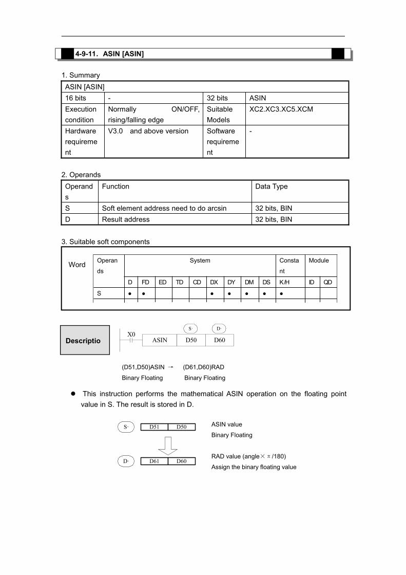
4-9-11.ASIN [ASIN]
1. SummaryASIN [ASIN]16 bits - 32 bits ASINExecutioncondition
Normally ON/OFF,rising/falling edge
SuitableModels
XC2.XC3.XC5.XCM
Hardwarerequirement
V3.0 and above version Softwarerequirement
-
2. OperandsOperands
Function Data Type
S Soft element address need to do arcsin 32 bits, BIND Result address 32 bits, BIN
3. Suitable soft components
ASIN D50 D60X0
S· D·
D51 D50
D61 D60
S·
D·
Operan
ds
System Consta
nt
Module
D FD ED TD CD DX DY DM DS K/H ID QD
S ● ● ● ● ● ● ●
D ● ● ● ●
Word
Descriptio
(D51,D50)ASIN → (D61,D60)RAD
Binary Floating Binary Floating
This instruction performs the mathematical ASIN operation on the floating pointvalue in S. The result is stored in D.
ASIN value
Binary Floating
RAD value (angle×π/180)
Assign the binary floating value
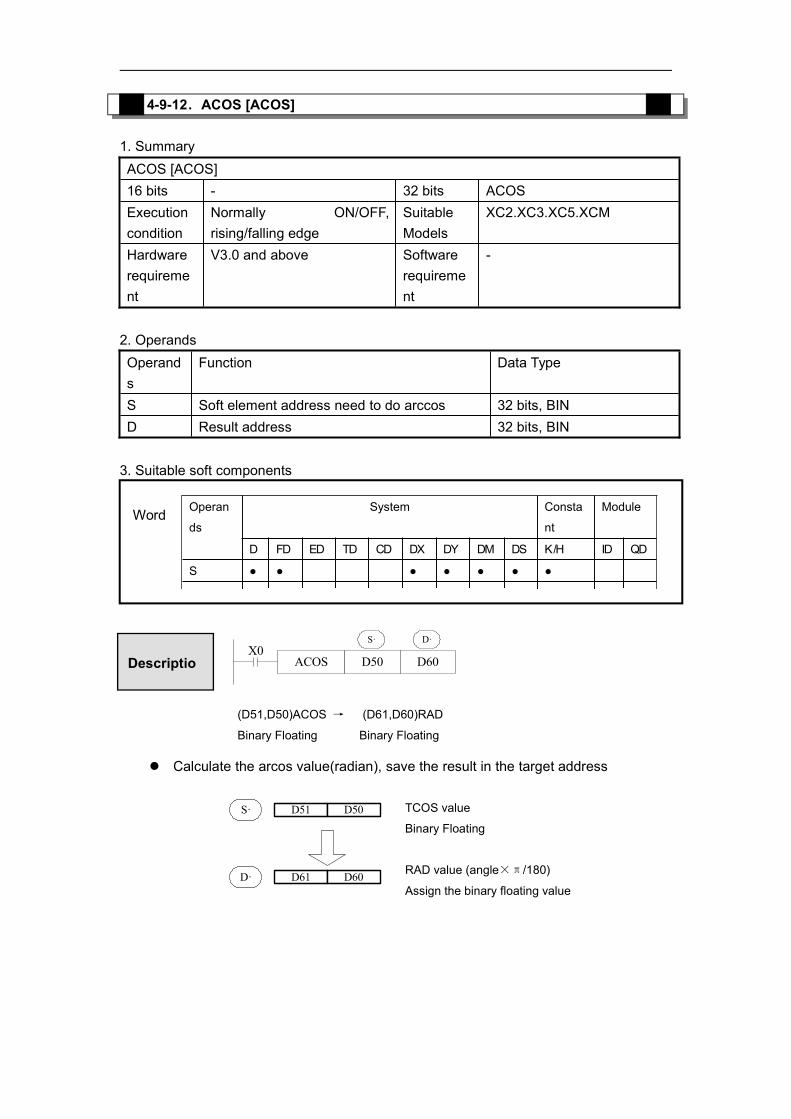
4-9-12.ACOS [ACOS]
1. SummaryACOS [ACOS]16 bits - 32 bits ACOSExecutioncondition
Normally ON/OFF,rising/falling edge
SuitableModels
XC2.XC3.XC5.XCM
Hardwarerequirement
V3.0 and above Softwarerequirement
-
2. OperandsOperands
Function Data Type
S Soft element address need to do arccos 32 bits, BIND Result address 32 bits, BIN
3. Suitable soft components
ACOS D50 D60X0
S· D·
D51 D50
D61 D60
S·
D·
Operan
ds
System Consta
nt
Module
D FD ED TD CD DX DY DM DS K/H ID QD
S ● ● ● ● ● ● ●
D ● ● ● ●
Word
Descriptio
(D51,D50)ACOS → (D61,D60)RAD
Binary Floating Binary Floating
Calculate the arcos value(radian), save the result in the target address
TCOS value
Binary Floating
RAD value (angle×π/180)
Assign the binary floating value

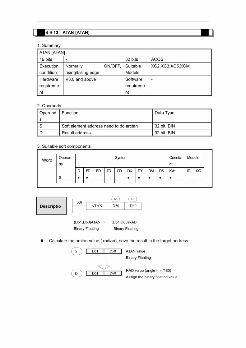
4-9-13.ATAN [ATAN]
1. SummaryATAN [ATAN]16 bits - 32 bits ACOSExecutioncondition
Normally ON/OFF,rising/falling edge
SuitableModels
XC2.XC3.XC5.XCM
Hardwarerequirement
V3.0 and above Softwarerequirement
-
2. OperandsOperands
Function Data Type
S Soft element address need to do arctan 32 bit, BIND Result address 32 bit, BIN
3. Suitable soft components
ATAN D50 D60X0
S· D·
D51 D50
D61 D60
S·
D·
Operan
ds
System Consta
nt
Module
D FD ED TD CD DX DY DM DS K/H ID QD
S ● ● ● ● ● ● ●
D ● ● ● ●
Word
Descriptio
(D51,D50)ATAN → (D61,D60)RAD
Binary Floating Binary Floating
Calculate the arctan value ( radian), save the result in the target address
ATAN value
Binary Floating
RAD value (angle×π/180)
Assign the binary floating value
4-10.RTC Instructions
Mnemonic Function ChapterTRD Clock data read 4-10-1TWR Clock data write 4-10-2
※1: To use the instructions, The Model should be equipped with RTC function;
4-10-1.Read the clock data [TRD]
1. Instruction SummaryRead the clock data:Read the clock data: [TRD]16 bits TRD 32 bits -Executioncondition
Normally ON/OFF,rising/falling edge
SuitableModels
XC2.XC3.XC5.XCM
Hardwarerequirement
V2.51 and above Softwarerequirement
-
2. OperandsOperands
Function Data Type
D Register to save clock data 16 bits, BIN
3. Suitable Soft Components
Word Operan
ds
System Consta
nt
Module
D FD ED TD CD DX DY DM DS K/H ID QD
D ● ● ●
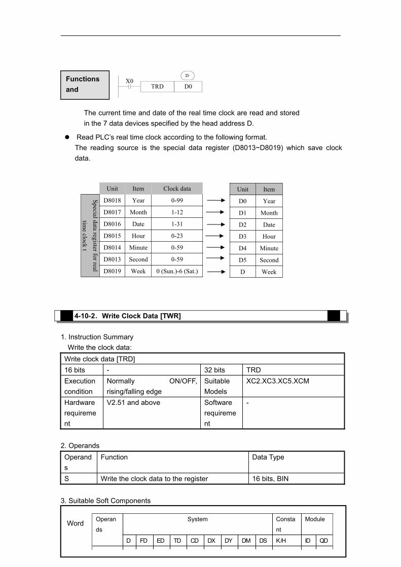
TRD D0X0
D·
Read PLC’s real time clock according to the following format.The reading source is the special data register (D8013~D8019) which save clockdata.
4-10-2.Write Clock Data [TWR]
1. Instruction SummaryWrite the clock data:Write clock data [TRD]16 bits - 32 bits TRDExecutioncondition
Normally ON/OFF,rising/falling edge
SuitableModels
XC2.XC3.XC5.XCM
Hardwarerequirement
V2.51 and above Softwarerequirement
-
2. OperandsOperands
Function Data Type
S Write the clock data to the register 16 bits, BIN
3. Suitable Soft Components
FunctionsandActions
The current time and date of the real time clock are read and storedin the 7 data devices specified by the head address D.
Unit Item
D0 Year
D1 Month
D2 Date
D3 Hour
D4 Minute
D5 Second
D Week
Unit Item Clock data
Specialdataregisterforreal
time
clockt
D8018 Year 0-99
D8017 Month 1-12
D8016 Date 1-31
D8015 Hour 0-23
D8014 Minute 0-59
D8013 Second 0-59
D8019 Week 0 (Sun.)-6 (Sat.)
Word Operan
ds
System Consta
nt
Module
D FD ED TD CD DX DY DM DS K/H ID QD
S ● ● ● ● ● ● ● ●
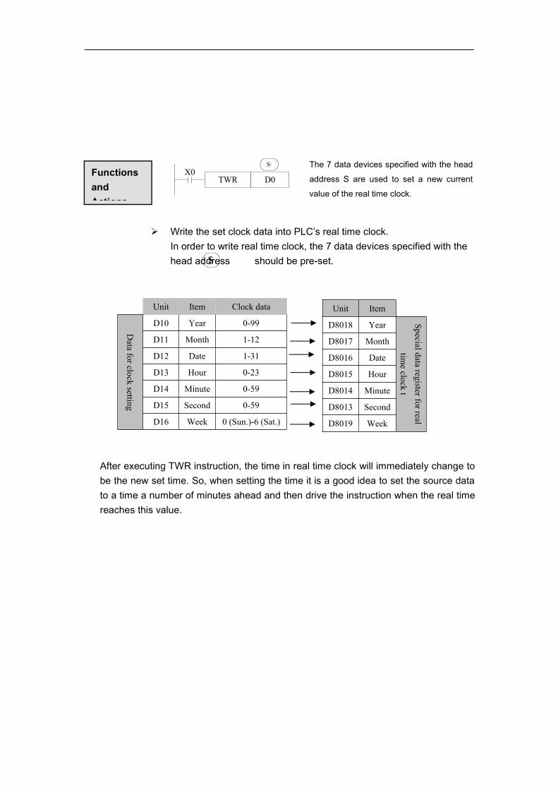
TWR D0X0
S· The 7 data devices specified with the head
address S are used to set a new current
value of the real time clock.
FunctionsandActions
Write the set clock data into PLC’s real time clock.In order to write real time clock, the 7 data devices specified with thehead address should be pre-set.S·
Unit Item Clock data
Data
forclocksetting
D10 Year 0-99
D11 Month 1-12
D12 Date 1-31
D13 Hour 0-23
D14 Minute 0-59
D15 Second 0-59
D16 Week 0 (Sun.)-6 (Sat.)
Unit Item
D8018 Year Specialdataregisterforreal
time
clockt
D8017 Month
D8016 Date
D8015 Hour
D8014 Minute
D8013 Second
D8019 Week
After executing TWR instruction, the time in real time clock will immediately change tobe the new set time. So, when setting the time it is a good idea to set the source datato a time a number of minutes ahead and then drive the instruction when the real timereaches this value.

5 High Speed Counter (HSC)
5 High speed counter (HSC)
In this chapter we tell high speed counter’s functions, including high speed count model,wiring method, read/write HSC value, reset etc.
5-1.FUNCTIONS SUMMARY
5-2.HIGH SPEED COUNTER’S MODE
5-3.HIGH SPEED COUNTER’S RANGE
5-4.INPUT WIRING OF HIGH SPEED COUNTER
5-5.INPUT TERMINALS ASSIGNMENT FOR HSC
5-6.READ AND WRITE THE HSC VALUE
5-7.RESET MODE OF HSC
5-8.FREQUENCY MULTIPLICATION OF AB PHASE HSC
5-9.HSC EXAMPLES
5-10.HSC INTERRUPTION

5 High Speed Counter (HSC)
Instructions List for HSC
MNEMONIC
FUNCTIONCIRCUIT AND SOFTCOMPONENTS
CHAPTER
READ/WRITE HIGH SPEED COUNTER
HSCR Read HSC 5-6-1
HSCW Write HSC 5-6-2
OUTHSC (High SpeedCounter)
3-13
OUT24 segments HSCInterruption
5-10
RST HSC Reset 3-13

5 High Speed Counter (HSC)
5-1.Functions Summary
XC series PLC has HSC (High Speed Counter) function which is independent withthe scan cycle. Via choosing different counter, test the high speed input signals with detectsensors and rotary encoders. The highest testing frequency can reach 80 KHz.
5-2.HSC Mode
XC series high speed counters function has three count modes: Increment Mode,Pulse + Direction Mode and AB phase Mode;
Under this mode, count and input the pulse signal, the count value increase at eachpulse’s rising edge;
Increment Mode
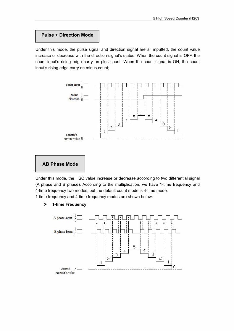
5 High Speed Counter (HSC)
Under this mode, the pulse signal and direction signal are all inputted, the count valueincrease or decrease with the direction signal’s status. When the count signal is OFF, thecount input’s rising edge carry on plus count; When the count signal is ON, the countinput’s rising edge carry on minus count;
Under this mode, the HSC value increase or decrease according to two differential signal(A phase and B phase). According to the multiplication, we have 1-time frequency and4-time frequency two modes, but the default count mode is 4-time mode.1-time frequency and 4-time frequency modes are shown below:
1-time Frequency
Pulse + Direction Mode
AB Phase Mode
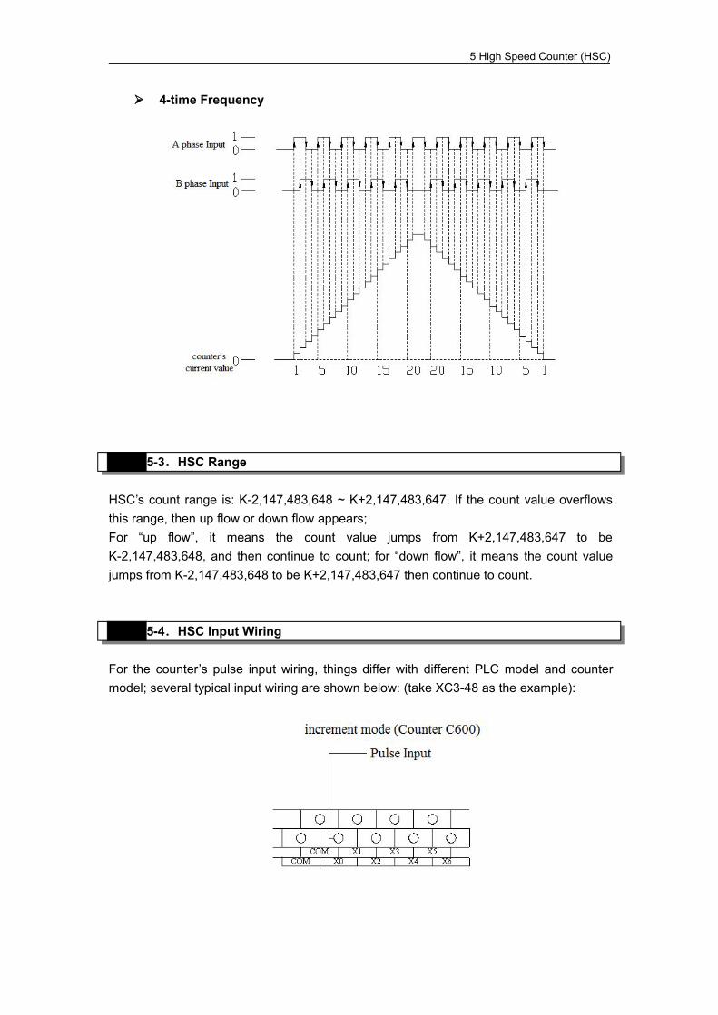
5 High Speed Counter (HSC)
4-time Frequency
5-3.HSC Range
HSC’s count range is: K-2,147,483,648 ~ K+2,147,483,647. If the count value overflowsthis range, then up flow or down flow appears;For “up flow”, it means the count value jumps from K+2,147,483,647 to beK-2,147,483,648, and then continue to count; for “down flow”, it means the count valuejumps from K-2,147,483,648 to be K+2,147,483,647 then continue to count.
5-4.HSC Input Wiring
For the counter’s pulse input wiring, things differ with different PLC model and countermodel; several typical input wiring are shown below: (take XC3-48 as the example):

5 High Speed Counter (HSC)
5-5.HSC ports assignment
Each letter’s meaning:U Dir A B
Pulse input Count Direction Judgment(OFF=increment, ON=decrement)
A phaseinput
B phase input
Normally, X0 and X1 can accept 80 KHz frequency under single phase mode and ABphase mode. Other terminals can accept only 10 KHz under single phase mode, 5 KHzunder AB phase mode. X can use as normal input terminals when they are not used ashigh speed input. The detailed assignment is shown as below:
XC2 series PLC
Increment Pulse+Dir InputAB PhaseMode
C600
C602
C604
C606
C608
C610
C612
C614
C616
C618
C620
C622
C624
C626
C628
C630
C632
C634
Max.F 80K 80K 10K 10K 10K 80K 10K 80K 5K4-times
F1/4 1
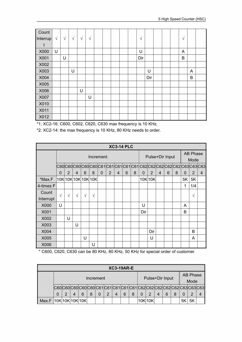
5 High Speed Counter (HSC)
*1: XC2-16: C600, C602, C620, C630 max frequency is 10 KHz.*2: XC2-14: the max frequency is 10 KHz, 80 KHz needs to order.
* C600, C620, C630 can be 80 KHz, 80 KHz, 50 KHz for special order of customer.
CountInterrup
t√ √ √ √ √ √ √
X000 U U AX001 U Dir BX002X003 U U AX004 Dir BX005X006 UX007 UX010X011X012
XC3-14 PLC
Increment Pulse+Dir InputAB PhaseMode
C600
C602
C604
C606
C608
C610
C612
C614
C616
C618
C620
C622
C624
C626
C628
C630
C632
C634
*Max.F 10K10K10K 10K 10K 10K10K 5K 5K4-times F 1 1/4CountInterrupt
√ √ √ √ √ √
X000 U U AX001 Dir BX002 UX003 UX004 Dir BX005 U U AX006 U
XC3-19AR-E
Increment Pulse+Dir InputAB PhaseMode
C600
C602
C604
C606
C608
C610
C612
C614
C616
C618
C620
C622
C624
C626
C628
C630
C632
C634
Max.F 10K10K 10K 10K 10K10K 5K 5K
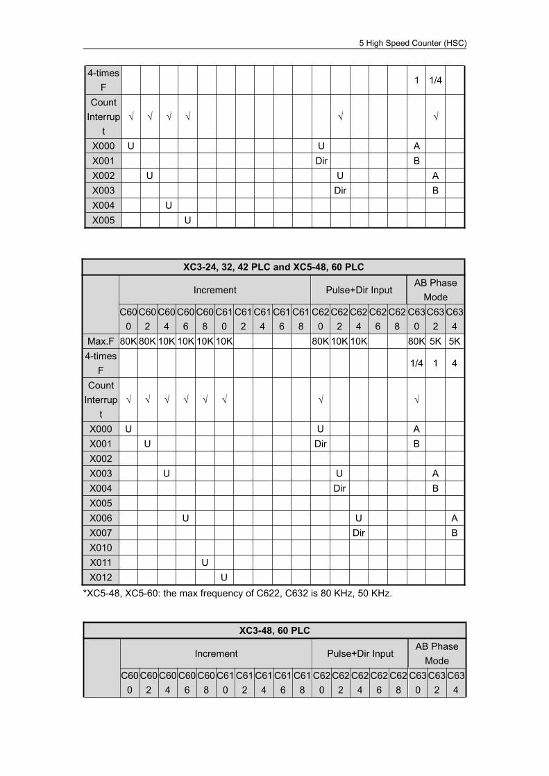
5 High Speed Counter (HSC)
*XC5-48, XC5-60: the max frequency of C622, C632 is 80 KHz, 50 KHz.
4-timesF
1 1/4
CountInterrup
t√ √ √ √ √ √
X000 U U AX001 Dir BX002 U U AX003 Dir BX004 UX005 U
XC3-24, 32, 42 PLC and XC5-48, 60 PLC
Increment Pulse+Dir InputAB PhaseMode
C600
C602
C604
C606
C608
C610
C612
C614
C616
C618
C620
C622
C624
C626
C628
C630
C632
C634
Max.F 80K 80K 10K 10K 10K 10K 80K 10K 10K 80K 5K 5K4-times
F1/4 1 4
CountInterrup
t√ √ √ √ √ √ √ √
X000 U U AX001 U Dir BX002X003 U U AX004 Dir BX005X006 U U AX007 Dir BX010X011 UX012 U
XC3-48, 60 PLC
Increment Pulse+Dir InputAB PhaseMode
C600
C602
C604
C606
C608
C610
C612
C614
C616
C618
C620
C622
C624
C626
C628
C630
C632
C634
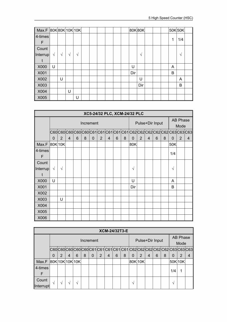
5 High Speed Counter (HSC)
XCM-24/32T3-E
Increment Pulse+Dir InputAB PhaseMode
C600
C602
C604
C606
C608
C610
C612
C614
C616
C618
C620
C622
C624
C626
C628
C630
C632
C634
Max.F 80K 10K 10K 10K 80K 10K 50K 10K4-times
F1/4 1
CountInterrupt
√ √ √ √ √ √
Max.F 80K 80K 10K 10K 80K 80K 50K 50K4-times
F1 1/4
CountInterrup
t√ √ √ √ √ √
X000 U U AX001 Dir BX002 U U AX003 Dir BX004 UX005 U
XC5-24/32 PLC, XCM-24/32 PLC
Increment Pulse+Dir InputAB PhaseMode
C600
C602
C604
C606
C608
C610
C612
C614
C616
C618
C620
C622
C624
C626
C628
C630
C632
C634
Max.F 80K 10K 80K 50K4-times
F1/4
CountInterrup
t√ √ √ √
X000 U U AX001 Dir BX002X003 UX004X005X006
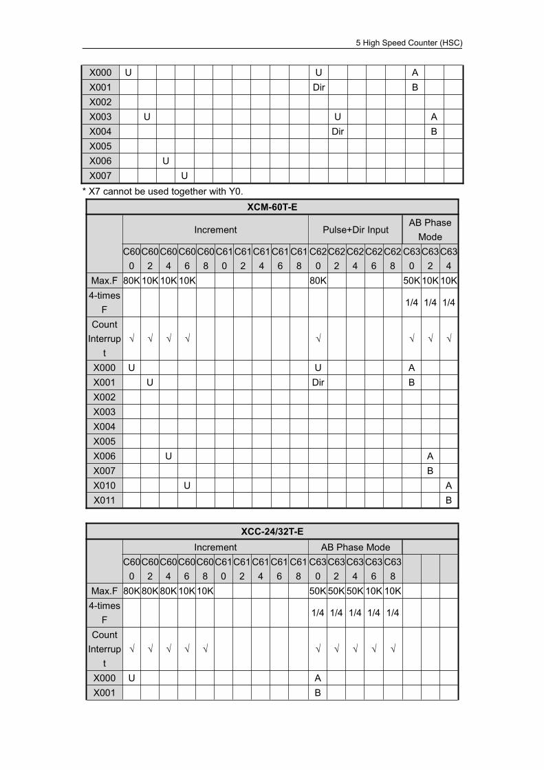
5 High Speed Counter (HSC)
X000 U U AX001 Dir BX002X003 U U AX004 Dir BX005X006 UX007 U
* X7 cannot be used together with Y0.XCM-60T-E
Increment Pulse+Dir InputAB PhaseMode
C600
C602
C604
C606
C608
C610
C612
C614
C616
C618
C620
C622
C624
C626
C628
C630
C632
C634
Max.F 80K10K10K10K 80K 50K10K10K4-times
F1/4 1/4 1/4
CountInterrup
t√ √ √ √ √ √ √ √
X000 U U AX001 U Dir BX002X003X004X005X006 U AX007 BX010 U AX011 B
XCC-24/32T-EIncrement AB Phase Mode
C600
C602
C604
C606
C608
C610
C612
C614
C616
C618
C630
C632
C634
C636
C638
Max.F 80K80K80K10K10K 50K50K50K 10K 10K4-times
F1/4 1/4 1/4 1/4 1/4
CountInterrup
t√ √ √ √ √ √ √ √ √ √
X000 U AX001 B
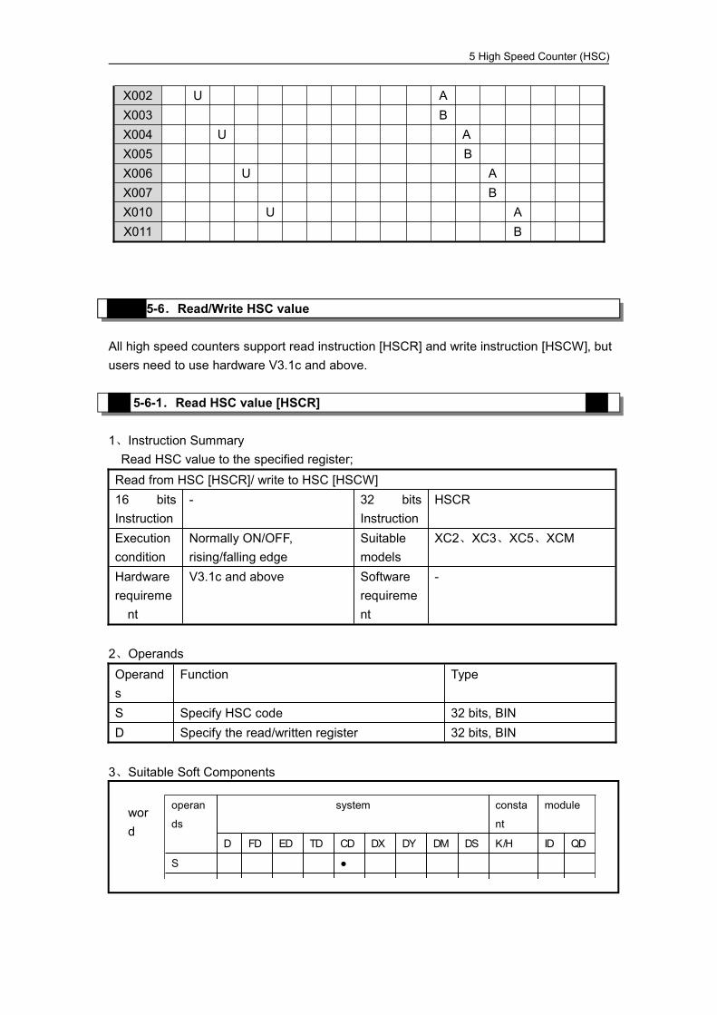
5 High Speed Counter (HSC)
X002 U AX003 BX004 U AX005 BX006 U AX007 BX010 U AX011 B
5-6.Read/Write HSC value
All high speed counters support read instruction [HSCR] and write instruction [HSCW], butusers need to use hardware V3.1c and above.
5-6-1.Read HSC value [HSCR]
1、Instruction SummaryRead HSC value to the specified register;Read from HSC [HSCR]/ write to HSC [HSCW]16 bitsInstruction
- 32 bitsInstruction
HSCR
Executioncondition
Normally ON/OFF,rising/falling edge
Suitablemodels
XC2、XC3、XC5、XCM
Hardwarerequirement
V3.1c and above Softwarerequirement
-
2、OperandsOperands
Function Type
S Specify HSC code 32 bits, BIND Specify the read/written register 32 bits, BIN
3、Suitable Soft Components
operan
ds
system consta
nt
module
D FD ED TD CD DX DY DM DS K/H ID QD
S ●
D ●
word

5 High Speed Counter (HSC)
HSCR C630 D10M0
S· D·
Sample Program:
5-6-2.Write HSC value [HSCW]
1、Instruction SummaryWrite the specified register value into HSC;Write HSC value [HSCW]16 bitsInstruction
- 32 bitsInstruction
HSCW
Executioncondition
Normally ON/OFF,rising/falling edge
Suitablemodels
XC2、XC3、XC5、XCM
Hardwarerequirement
V3.1c and above Softwarerequirement
-
FUNCTIONS AND ACTIONS
When the activate condition is true, read the HSC value in C630 (DWORD)into D10 (DWORD)
Instruction HSCR read the HSC value into the specified register, improveHSC value’s precision.
Note: For hardware version larger than 3.1, please use HSCR to move thehigh speed counter value to the register. DMOV instruction cannot be used.
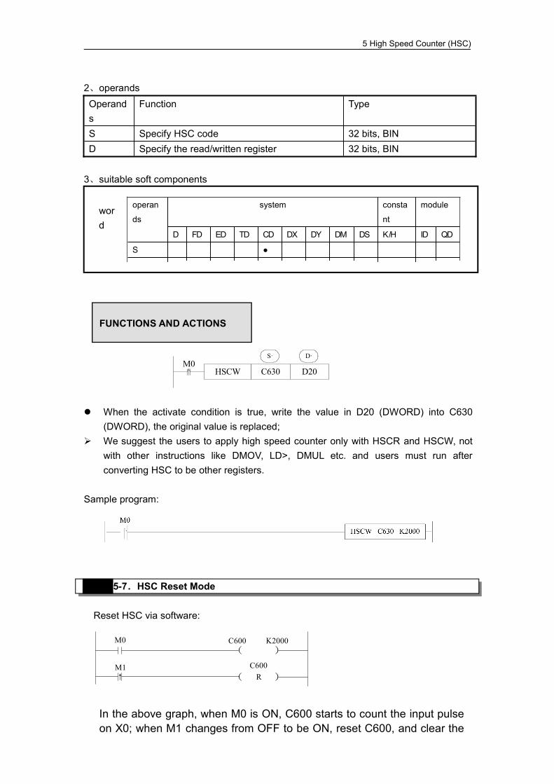
5 High Speed Counter (HSC)
2、operandsOperands
Function Type
S Specify HSC code 32 bits, BIND Specify the read/written register 32 bits, BIN
3、suitable soft components
HSCW C630 D20M0
S· D·
When the activate condition is true, write the value in D20 (DWORD) into C630(DWORD), the original value is replaced;
We suggest the users to apply high speed counter only with HSCR and HSCW, notwith other instructions like DMOV, LD>, DMUL etc. and users must run afterconverting HSC to be other registers.
Sample program:
5-7.HSC Reset Mode
Reset HSC via software:
M0
M1
( )C600 K2000
( )C600
R↑
operan
ds
system consta
nt
module
D FD ED TD CD DX DY DM DS K/H ID QD
S ●
D ●
word
FUNCTIONS AND ACTIONS
In the above graph, when M0 is ON, C600 starts to count the input pulseon X0; when M1 changes from OFF to be ON, reset C600, and clear the
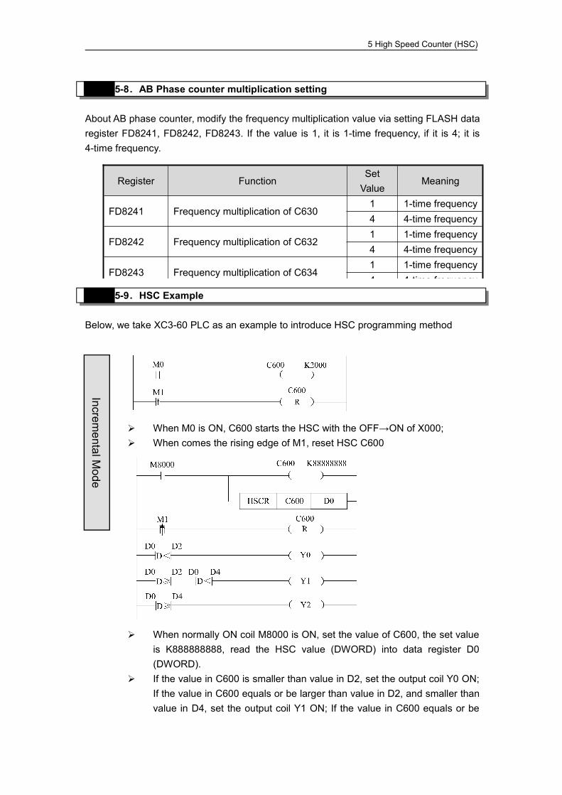
5 High Speed Counter (HSC)
5-8.AB Phase counter multiplication setting
About AB phase counter, modify the frequency multiplication value via setting FLASH dataregister FD8241, FD8242, FD8243. If the value is 1, it is 1-time frequency, if it is 4; it is4-time frequency.
Register FunctionSetValue
Meaning
FD8241 Frequency multiplication of C6301 1-time frequency4 4-time frequency
FD8242 Frequency multiplication of C6321 1-time frequency4 4-time frequency
FD8243 Frequency multiplication of C6341 1-time frequency4 4-time frequency
5-9.HSC Example
Below, we take XC3-60 PLC as an example to introduce HSC programming method
When M0 is ON, C600 starts the HSC with the OFF→ON of X000; When comes the rising edge of M1, reset HSC C600
When normally ON coil M8000 is ON, set the value of C600, the set valueis K888888888, read the HSC value (DWORD) into data register D0(DWORD).
If the value in C600 is smaller than value in D2, set the output coil Y0 ON;If the value in C600 equals or be larger than value in D2, and smaller thanvalue in D4, set the output coil Y1 ON; If the value in C600 equals or be
IncrementalM
ode
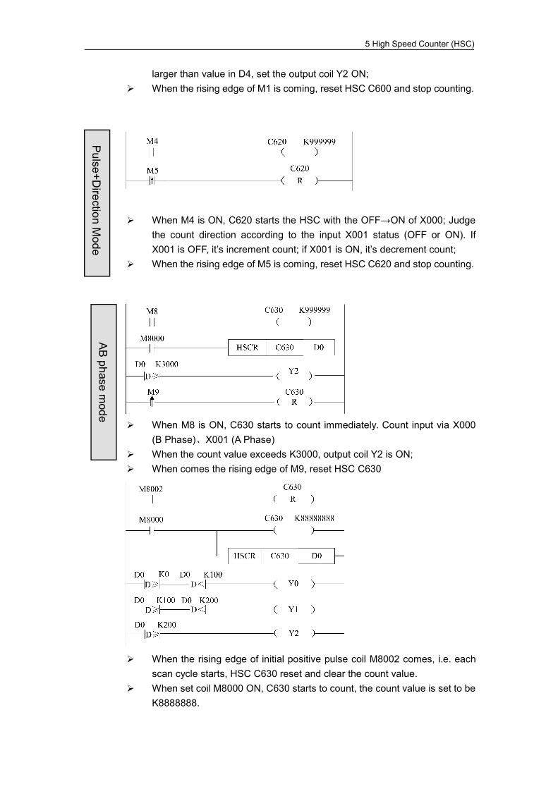
5 High Speed Counter (HSC)
larger than value in D4, set the output coil Y2 ON; When the rising edge of M1 is coming, reset HSC C600 and stop counting.
When M4 is ON, C620 starts the HSC with the OFF→ON of X000; Judgethe count direction according to the input X001 status (OFF or ON). IfX001 is OFF, it’s increment count; if X001 is ON, it’s decrement count;
When the rising edge of M5 is coming, reset HSC C620 and stop counting.
When M8 is ON, C630 starts to count immediately. Count input via X000(B Phase)、X001 (A Phase)
When the count value exceeds K3000, output coil Y2 is ON; When comes the rising edge of M9, reset HSC C630
When the rising edge of initial positive pulse coil M8002 comes, i.e. eachscan cycle starts, HSC C630 reset and clear the count value.
When set coil M8000 ON, C630 starts to count, the count value is set to beK8888888.
Pulse+D
irectionMode
ABphase
mode
5 High Speed Counter (HSC)
If the count value is greater than K0 but smaller than K100, the output coilY0 set ON; If the count value is greater than K100 but smaller than K200,the output coil Y1 set ON; If the count value is greater thanK200, theoutput coil Y2 set ON;
To XC series PLC, each HSC channels has 24 segments 32-bit pre-set value. Whenthe HSC difference value equals the correspond 24-segment pre-set value, theninterruption occurs according to the interruption tag;
To use this function, please use hardware V3.1c or above;
(For the program about interruption, please refer chapter 5-10-4)
LD M0 //HSC activates condition M0 (interruption countcondition)OUT C600 K20000 D4000 //HSC value and set the start ID of
24-segmentLDP M1 //activate condition of resetRST C600 //HSC and 24-segment reset(interruption reset)
As shown in the above graph, data register D4000 is the start ID of 24-segmentpre-set value area. Behind it, save each pre-set value in DWORD form. Please payattention when using HSC: If certain pre-set value is 0, it means count interruption end at this segment; Set the interruption pre-set value but not write the correspond interruption program
is not allowed; 24-segment interruption of HSC occurs in order. If the first segment interruption
doesn't happen, then the second segment interruption will not happen; 24-segment pre-set value can be specified to be relative value or absolute value.
Meantime, users can specify the value to be loop or not. But the loop mode can't beused together with absolute value. (Please refer to special coil M8190~M8209,M8270~M8287).
5-10. HSC Interruption
5-10-1. Instruction Description

5 High Speed Counter (HSC)
Counte
r
Interruption tag
C630 I2501~I2524
C632 I2601~I2624
C634 I2701~I2724
C636 I2801~I2824
C638 I2901~I2924
In the below table, we list each counter's 24-segment pre-set value to its interruption tag.I.e.: 24-segment pre-set value of counter C600 correspond with the interruption pointer:I1001, I1002, and I1003 …I1024.
Increment mode pulse + direction mode AB phase mode
E.g. 1, the current value is C630 is 0, the first preset value is 10000, the preset value insegment 2 is -5000, and the present value in segment 3 is 20000. When start to count,the counter's current value is 10000, generate first interruption I2501; When start to count,the counter's current value is 5000, generate first interruption I2502; When start to count,the counter's current value is 25000, generate first interruption I2503.
See graph below:
Counte
r
Interruption tag
C600 I1001~I1024
C602 I1101~I1124
C604 I1201~I1224
C606 I1301~I1324
C608 I1401~I1424
C610 I1501~I1524
C612 I1601~I1624
C614 I1701~I1724
C616 I1801~I1824
C618 I1901~I1924
Counte
r
Interruption tag
C620 I2001~I2024
C622 I2101~I2124
C624 I2201~I2224
C626 I2301~I2324
C628 I2401~I2424
HSC 24-segment pre-set value is the difference value, the count value equals thecounter's current value plus the preset value, generate the interruption. N interruptiontags correspond with N interruption preset values. The (N+1) preset value is 0;
Define the present
5-10-2. Interruption tags to HSC

5 High Speed Counter (HSC)
C600= K5000+K20000=K25000
C600= K10000+(K-5000)=K5000
C600=
C630 D4000 D4001 D4002 D4003 D4004 D4005
K0 K10000 K-5000 K20000
I2501
I2502
I2503
E.g. 2, the current value is C630 is 10000, the first preset value is 10000, the preset valuein segment 2 is 5000, and the preset value in segment 3 is 20000. When start to count,the counter's current value is 20000, generate first interruption I2501; When start to count,the counter's current value is 25000, generate first interruption I2502;When start to count,the counter's current value is 45000, generate first interruption I2503.
See graph below:
C600= K25000+K20000=K45000
C600= K20000+K5000=K25000
C600=
C630 D4000 D4001 D4002
D4003 D4004 D4005
K10000 K10000 K5000 K20000
I2501
I2502
I2503
Mode 1: Single loop (normal mode)Not happen after HSC interruption ends. The conditions below can re-start the
interruption: reset the HSC Reboot the HSC activate condition
Mode 2: Continuous loop
5-10-3. Loop mode of HSC Interruption
5 High Speed Counter (HSC)
Restart after HSC interruption ends. This mode is especially suitable for the followingapplication:
continuous back-forth movement Generate cycle interruption according to the defined pulse
Via setting the special auxiliary relays, users can set the HSC interruption to be unicyclemode or continuous loop mode. The loop mode is only suitable with the relative count.The detailed assignment is show below:
ID HSC ID Setting
M827024 segments HSC interruption loop(C600)
OFF: single loop modeON: continuous loopmode
M827124 segments HSC interruption loop(C602)
M827224 segments HSC interruption loop(C604)
M827324 segments HSC interruption loop(C606)
M827424 segments HSC interruption loop(C608)
M827524 segments HSC interruption loop(C610)
M827624 segments HSC interruption loop(C612)
M827724 segments HSC interruption loop(C614)
M827824 segments HSC interruption loop(C616)
M827924 segments HSC interruption loop(C618)
M828024 segments HSC interruption loop(C620)
M828124 segments HSC interruption loop(C622)
M828224 segments HSC interruption loop(C624)
M828324 segments HSC interruption loop(C626)
M828424 segments HSC interruption loop(C628)
M828524 segments HSC interruption loop(C630)
M8286 24 segments HSC interruption loop
5 High Speed Counter (HSC)
(C632)
M828724 segments HSC interruption loop(C634)
E.g.1: when M0 is ON, C630 starts counting from D4000. When it reaches the presentvalue, the interruption is produced. When the rising edge of M1 is coming, clear the C630.
DMOV K10000 D4000M8000
DMOV K-10000 D4002
DMOV K0 D4004
FEND
I2501
M0 C630 K200000 D4000( )
M1( )
C630R
M8000INC D0
IRET
I2502
M8000INC D1
IRET
E.g.2: Application on knit-weaving machine (continuous loop mode)The system theory is shown as below: Control the inverter via PLC, thereby control themotor. Meantime, via the feedback signal from encoder, control the knit-weaving machineand realize the precise position.
5-10-4. Example of HSC Interruption
5 High Speed Counter (HSC)
Below is PLC program: Y2 represents forward output signal; Y3 represents backwardoutput signal; Y4 represents output signal of speed 1; C340: Back-forth time’saccumulation counter; C630: AB phase HSC;

5 High Speed Counter (HSC)
FEND
I2501
M8000 Y4S
IRET
IRET
M8000( )
M8285S
Y2S( )
Y2OUT C340 K1000000
DMOV K75000 D4000M8000
DMOV K15000 D4002
DMOV K-75000 D4004
DMOV K-15000 D4006
M8000OUT C630 D4000K30000000
M8000HSCR C630 D200
( )
I2502
M8000 Y4R( )
Y2R( )
Y3S( )
I2503
M8000 Y4S( )
IRET
I2504
IRET
M8000 Y3R( )
Y4R( )
Y2S( )
5 High Speed Counter (HSC)
Instruction List Form:
LD M8002 //M8002 is initial positive pulse coilSETM8285 //special auxiliary relay set ON, to enable C630continuous loopSETY2 //set output coil Y2 (i.e. Start run forth)LDPY2 //knit-weaving machine back-forth times counter's activate condition Y2 (forthrising edge activate)OUT C340 K1000000 //counter C340 starts to countLD M8000 //M8000 is normally ON coilDMOV K75000 D4000 //set segment-1 ID D4000 to be K75000,DMOV K15000 D4002 //set segment-2 D4002 to be K15000,DMOV K-75000 D4004 //set segment-3 D4004 to be K-75000,DMOV K-15000 D4006 //set segment-4 D4004 to be K-15000,LD M8000 //M8000 is normally ON coilOUT C630 K30000000 D4000 //HSC and start ID of 24-segmentLD M8000 //M8000 is normally ON coilHSCR C630 D200 //read the HSC value of C630 to D200FEND //main program endI2501 //interruption tag of segment 1LD M8000 //M8000 is normally ON coilSET Y4 //output coil Y4 set (low-speed run with speed 1)IRET //interruption return tagI2502 ///interruption tag of segment 2LD M8000 //M8000 is normally ON coilRST Y4 //output coil Y4 reset (low-speed run stop)RST Y2 //output coil Y2 reset (run forward stops)SETY3 //output coil Y3 set (back running)IRET //interruption return tagI2503 ///interruption tag of segment 3LD M8000 //M8000 is normally ON coilSETY4 //output coil Y4 set (low-speed run with speed 1)IRET //interruption return tagI2504 ///interruption tag of segment 4LD M8000 //M8000 is normally ON coilRST Y3 //output coil Y3 reset (back running stop)RST Y4 //output coil Y4 reset (low-speed run stop)SETY2 //output coil Y2 set (run forward)IRET //interruption return tag
6 Pulse Output
6 PULSE OUTPUT
In this chapter we will tell the pulse function of XC series PLC. The content includes pulseoutput instructions, input/output wiring, notes, and relate coils and registers etc.
6-1.Functions Summary
6-2.Pulse Output Types and Instructions
6-3.Output Wiring
6-4.Notes
6-5.Sample Programs
6-6.Coils and Registers Relate To Pulse Output

6 Pulse Output
Pulse Output Instructions List
Mnemonic Function Circuit And Soft Device Chapter
PULSE OUTPUT
PLSY
Unidirectionalration pulseoutput withoutACC/DECtime change
PLSY S1 S2 D 6-2-1
PLSFVariablefrequencypulse output
PLSF S D 6-2-2
PLSR
Ration pulseoutput withACC/DECspeed
PLSR S1 S2 S3 D 6-2-3
PLSNEXT/PLSNT
Pulse SectionSwitch
PLSNT S 6-2-4
STOP Pulse Stop STOP S 6-2-5
PLSMVRefresh PulseNr.immediately
PLSMV S D 6-2-6
ZRNOriginalReturn
ZRN S1 S2 S3 D 6-2-7
DRVIRelativePositionControl
DRVI S1 S2 S3 D1 D2 6-2-8
DRVAAbsolutePositionControl
DRVA S1 S2 S3 D1 D2 6-2-9
PLSA
AbsolutePositionmulti-sectionpulse control
PLSA S1 S2 D 6-2-10
PTO
Relativepositionmulti-sectionpulse control
6-2-11
PTOA
Absolutepositionmulti-sectionpulse control
6-2-12
PTO D0 Y0M0 S1· D1·
Y1
D2·
PTOA D0 Y0M0 S1· D1·
Y1
D2·
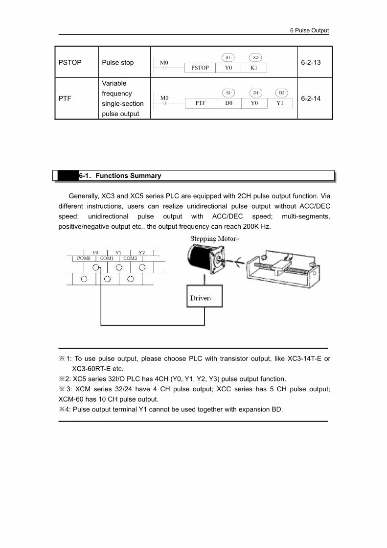
6 Pulse Output
PSTOP Pulse stop 6-2-13
PTF
Variablefrequencysingle-sectionpulse output
6-2-14
6-1.Functions Summary
Generally, XC3 and XC5 series PLC are equipped with 2CH pulse output function. Viadifferent instructions, users can realize unidirectional pulse output without ACC/DECspeed; unidirectional pulse output with ACC/DEC speed; multi-segments,positive/negative output etc., the output frequency can reach 200K Hz.
※1: To use pulse output, please choose PLC with transistor output, like XC3-14T-E orXC3-60RT-E etc.
※2: XC5 series 32I/O PLC has 4CH (Y0, Y1, Y2, Y3) pulse output function.※ 3: XCM series 32/24 have 4 CH pulse output; XCC series has 5 CH pulse output;XCM-60 has 10 CH pulse output.※4: Pulse output terminal Y1 cannot be used together with expansion BD.
PSTOP Y0 K1M0
S1· S2·
PTF D0 Y0M0
S1· D1·
Y1
D2·
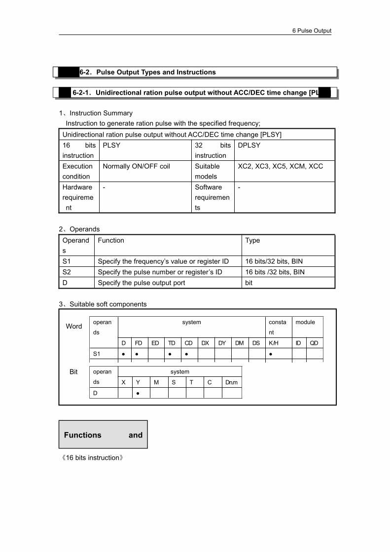
6 Pulse Output
6-2.Pulse Output Types and Instructions
6-2-1.Unidirectional ration pulse output without ACC/DEC time change [PLSY]
1、Instruction SummaryInstruction to generate ration pulse with the specified frequency;Unidirectional ration pulse output without ACC/DEC time change [PLSY]16 bitsinstruction
PLSY 32 bitsinstruction
DPLSY
Executioncondition
Normally ON/OFF coil Suitablemodels
XC2, XC3, XC5, XCM, XCC
Hardwarerequirement
- Softwarerequirements
-
2、OperandsOperands
Function Type
S1 Specify the frequency’s value or register ID 16 bits/32 bits, BINS2 Specify the pulse number or register’s ID 16 bits /32 bits, BIND Specify the pulse output port bit
3、Suitable soft components
《16 bits instruction》
operan
ds
system consta
nt
module
D FD ED TD CD DX DY DM DS K/H ID QD
S1 ● ● ● ● ●
S2 ● ● ● ● ●
Word
operan
ds
system
X Y M S T C Dn.m
D ●
Bit
Functions and
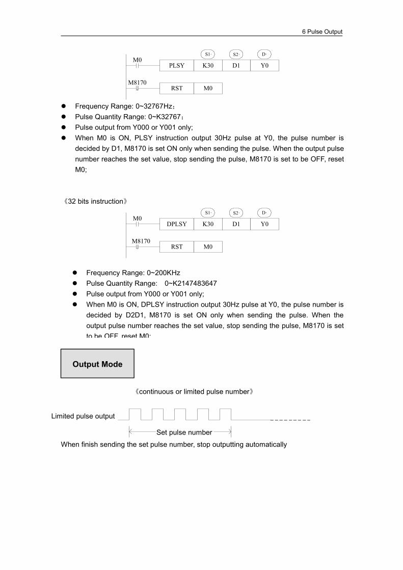
6 Pulse Output
PLSY K30 D1 Y0M0
S1· S2· D·
M8170RST M0
Frequency Range: 0~32767Hz; Pulse Quantity Range: 0~K32767; Pulse output from Y000 or Y001 only; When M0 is ON, PLSY instruction output 30Hz pulse at Y0, the pulse number is
decided by D1, M8170 is set ON only when sending the pulse. When the output pulsenumber reaches the set value, stop sending the pulse, M8170 is set to be OFF, resetM0;
《32 bits instruction》
DPLSY K30 D1 Y0M0
S1· S2· D·
M8170RST M0
《continuous or limited pulse number》
When finish sending the set pulse number, stop outputting automatically
Frequency Range: 0~200KHz Pulse Quantity Range: 0~K2147483647 Pulse output from Y000 or Y001 only; When M0 is ON, DPLSY instruction output 30Hz pulse at Y0, the pulse number is
decided by D2D1, M8170 is set ON only when sending the pulse. When theoutput pulse number reaches the set value, stop sending the pulse, M8170 is setto be OFF, reset M0;
Output Mode
Limited pulse output
Set pulse number

6 Pulse Output
Note: T1 is pulse start time, T2 is pulse end time.
Pulse frequency=1000Hz, pulse quantity 20K, no acceleration/deceleration and singledirection pulse output:
Note: D0 is pulse frequency, D2 is pulse quantity. D0=1000, D2=20000.
If the control object is stepping/servo motor, we recommend users not use this instruction,to avoid the motor losing synchronism. PLSR is available.
6-2-2.Variable Pulse Output [PLSF]
PLSF has 4 control modes.Mode 1: changeable frequency continuous pulse output PLSF1、Instruction SummaryInstruction to generate continuous pulse in the form of variable frequencyVariable Pulse Output [PLSF]
Items to Note
Example
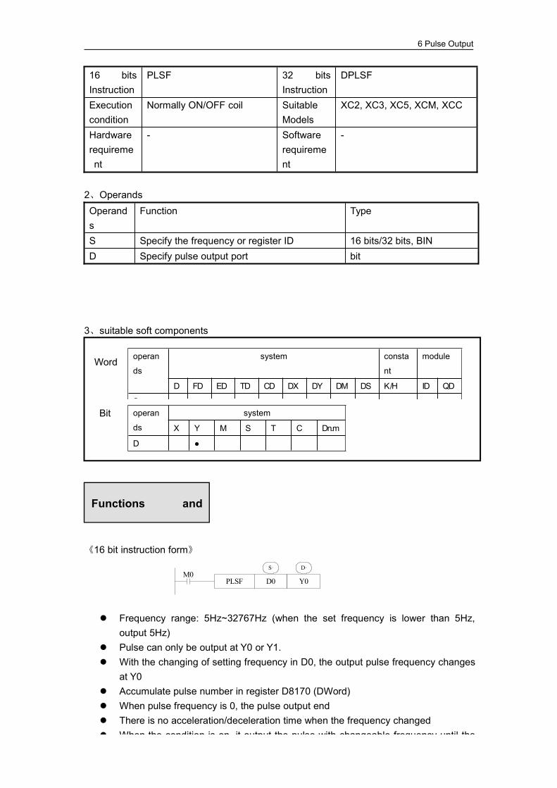
6 Pulse Output
16 bitsInstruction
PLSF 32 bitsInstruction
DPLSF
Executioncondition
Normally ON/OFF coil SuitableModels
XC2, XC3, XC5, XCM, XCC
Hardwarerequirement
- Softwarerequirement
-
2、OperandsOperands
Function Type
S Specify the frequency or register ID 16 bits/32 bits, BIND Specify pulse output port bit
3、suitable soft components
《16 bit instruction form》
PLSF D0 Y0M0
S· D·
Frequency range: 5Hz~32767Hz (when the set frequency is lower than 5Hz,output 5Hz)
Pulse can only be output at Y0 or Y1. With the changing of setting frequency in D0, the output pulse frequency changes
at Y0 Accumulate pulse number in register D8170 (DWord) When pulse frequency is 0, the pulse output end There is no acceleration/deceleration time when the frequency changed When the condition is on, it output the pulse with changeable frequency until the
operan
ds
system consta
nt
module
D FD ED TD CD DX DY DM DS K/H ID QD
S ● ● ● ● ●
Word
operan
ds
system
X Y M S T C Dn.m
D ●
Bit
Functions and
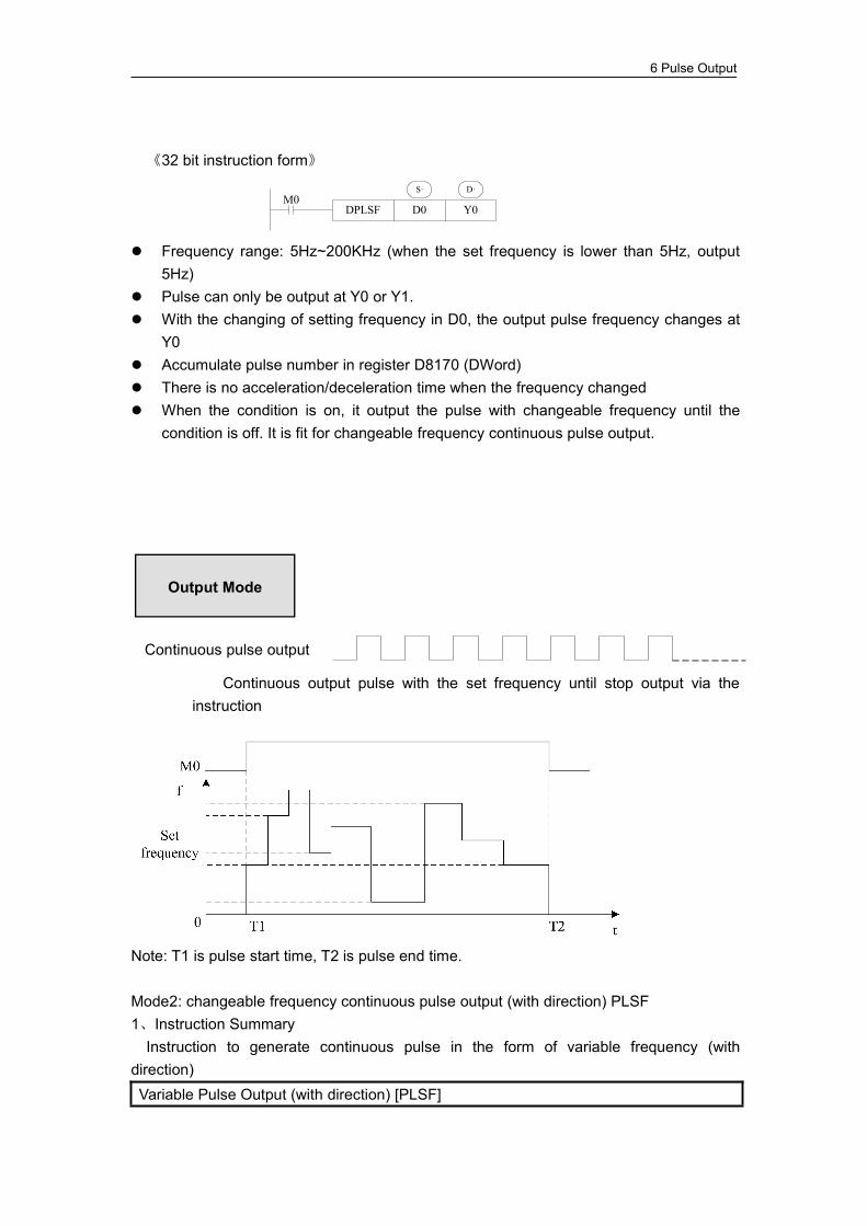
6 Pulse Output
《32 bit instruction form》
DPLSF D0 Y0M0
S· D·
Frequency range: 5Hz~200KHz (when the set frequency is lower than 5Hz, output5Hz)
Pulse can only be output at Y0 or Y1. With the changing of setting frequency in D0, the output pulse frequency changes at
Y0 Accumulate pulse number in register D8170 (DWord) There is no acceleration/deceleration time when the frequency changed When the condition is on, it output the pulse with changeable frequency until the
condition is off. It is fit for changeable frequency continuous pulse output.
Continuous output pulse with the set frequency until stop output via theinstruction
Note: T1 is pulse start time, T2 is pulse end time.
Mode2: changeable frequency continuous pulse output (with direction) PLSF1、Instruction SummaryInstruction to generate continuous pulse in the form of variable frequency (with
direction)Variable Pulse Output (with direction) [PLSF]
Continuous pulse output
Output Mode
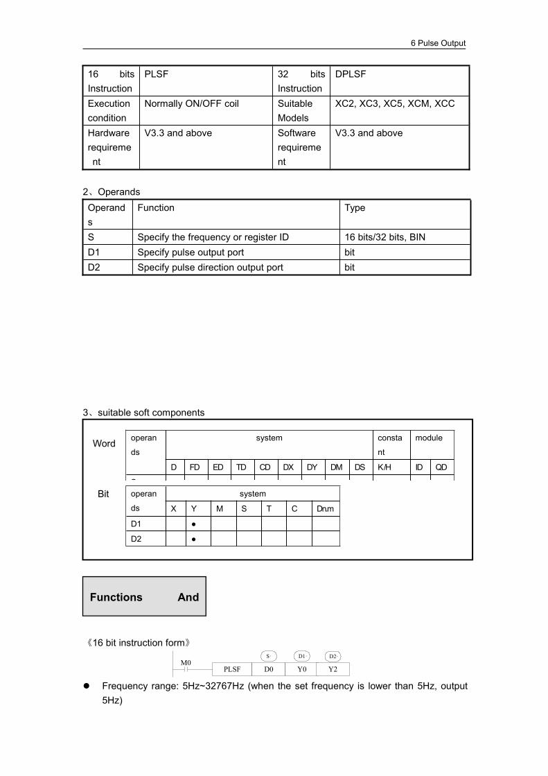
6 Pulse Output
16 bitsInstruction
PLSF 32 bitsInstruction
DPLSF
Executioncondition
Normally ON/OFF coil SuitableModels
XC2, XC3, XC5, XCM, XCC
Hardwarerequirement
V3.3 and above Softwarerequirement
V3.3 and above
2、OperandsOperands
Function Type
S Specify the frequency or register ID 16 bits/32 bits, BIND1 Specify pulse output port bitD2 Specify pulse direction output port bit
3、suitable soft components
《16 bit instruction form》
PLSF D0 Y0M0
S· D1·
Y2
D2·
Frequency range: 5Hz~32767Hz (when the set frequency is lower than 5Hz, output5Hz)
operan
ds
system consta
nt
module
D FD ED TD CD DX DY DM DS K/H ID QD
S ● ● ● ● ●
Word
operan
ds
system
X Y M S T C Dn.m
D1 ●
D2 ●
Bit
Functions And
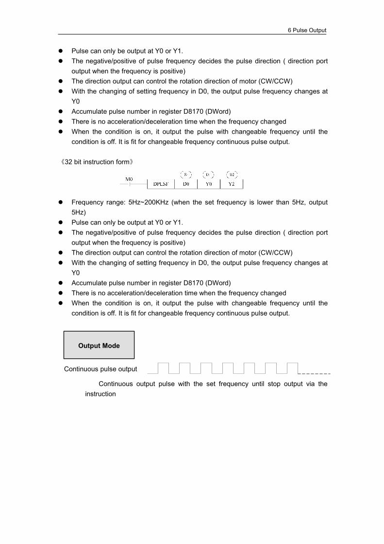
6 Pulse Output
Pulse can only be output at Y0 or Y1. The negative/positive of pulse frequency decides the pulse direction ( direction port
output when the frequency is positive) The direction output can control the rotation direction of motor (CW/CCW) With the changing of setting frequency in D0, the output pulse frequency changes at
Y0 Accumulate pulse number in register D8170 (DWord) There is no acceleration/deceleration time when the frequency changed When the condition is on, it output the pulse with changeable frequency until the
condition is off. It is fit for changeable frequency continuous pulse output.
《32 bit instruction form》
Frequency range: 5Hz~200KHz (when the set frequency is lower than 5Hz, output5Hz)
Pulse can only be output at Y0 or Y1. The negative/positive of pulse frequency decides the pulse direction ( direction port
output when the frequency is positive) The direction output can control the rotation direction of motor (CW/CCW) With the changing of setting frequency in D0, the output pulse frequency changes at
Y0 Accumulate pulse number in register D8170 (DWord) There is no acceleration/deceleration time when the frequency changed When the condition is on, it output the pulse with changeable frequency until the
condition is off. It is fit for changeable frequency continuous pulse output.
Continuous output pulse with the set frequency until stop output via theinstruction
Continuous pulse output
Output Mode
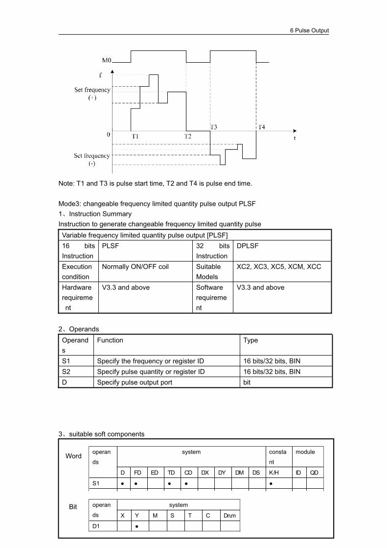
6 Pulse Output
Note: T1 and T3 is pulse start time, T2 and T4 is pulse end time.
Mode3: changeable frequency limited quantity pulse output PLSF1、Instruction SummaryInstruction to generate changeable frequency limited quantity pulseVariable frequency limited quantity pulse output [PLSF]16 bitsInstruction
PLSF 32 bitsInstruction
DPLSF
Executioncondition
Normally ON/OFF coil SuitableModels
XC2, XC3, XC5, XCM, XCC
Hardwarerequirement
V3.3 and above Softwarerequirement
V3.3 and above
2、OperandsOperands
Function Type
S1 Specify the frequency or register ID 16 bits/32 bits, BINS2 Specify pulse quantity or register ID 16 bits/32 bits, BIND Specify pulse output port bit
3、suitable soft components
operan
ds
system consta
nt
module
D FD ED TD CD DX DY DM DS K/H ID QD
S1 ● ● ● ● ●
S2 ● ● ● ● ●
Word
operan
ds
system
X Y M S T C Dn.m
D1 ●
Bit
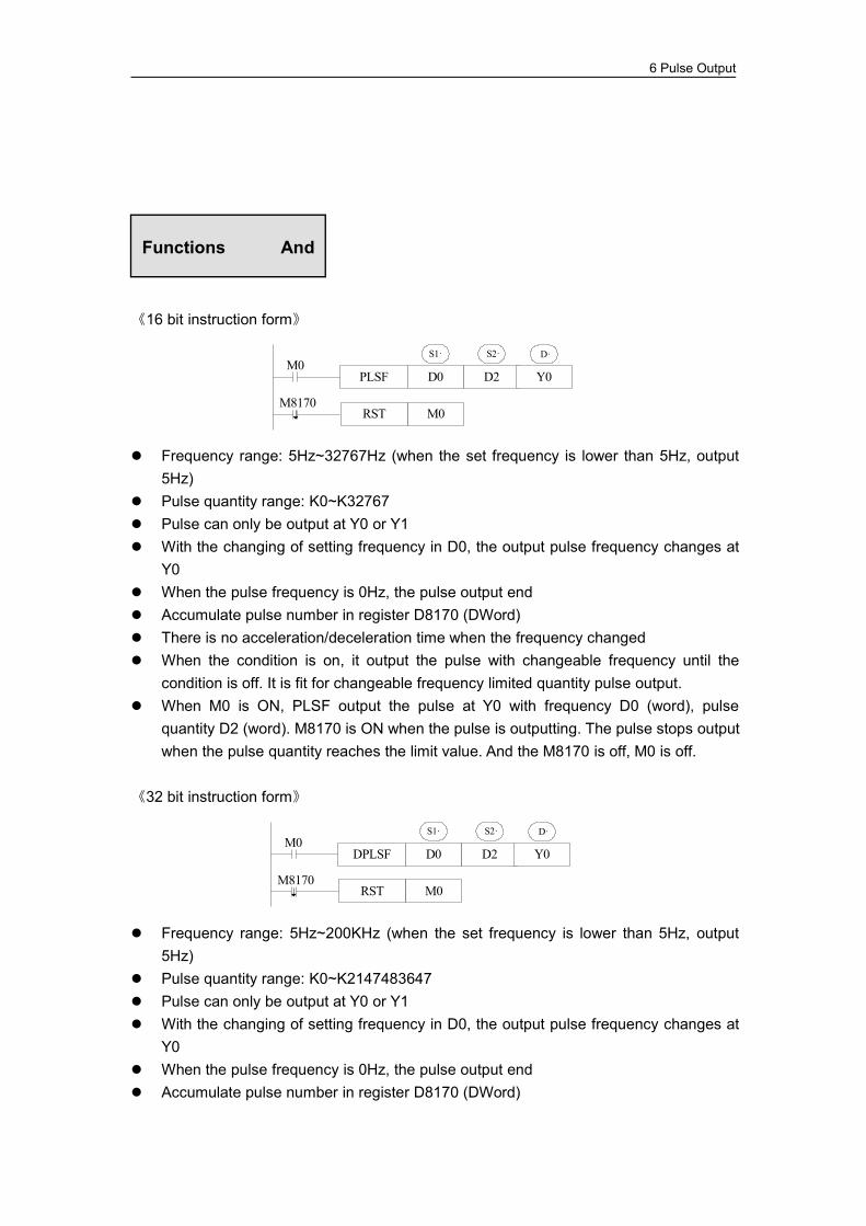
6 Pulse Output
《16 bit instruction form》
PLSF D0 D2M0
S1· S2·
Y0
D·
M8170RST M0
Frequency range: 5Hz~32767Hz (when the set frequency is lower than 5Hz, output5Hz)
Pulse quantity range: K0~K32767 Pulse can only be output at Y0 or Y1 With the changing of setting frequency in D0, the output pulse frequency changes at
Y0 When the pulse frequency is 0Hz, the pulse output end Accumulate pulse number in register D8170 (DWord) There is no acceleration/deceleration time when the frequency changed When the condition is on, it output the pulse with changeable frequency until the
condition is off. It is fit for changeable frequency limited quantity pulse output. When M0 is ON, PLSF output the pulse at Y0 with frequency D0 (word), pulse
quantity D2 (word). M8170 is ON when the pulse is outputting. The pulse stops outputwhen the pulse quantity reaches the limit value. And the M8170 is off, M0 is off.
《32 bit instruction form》
DPLSF D0 D2M0
S1· S2·
Y0
D·
M8170RST M0
Frequency range: 5Hz~200KHz (when the set frequency is lower than 5Hz, output5Hz)
Pulse quantity range: K0~K2147483647 Pulse can only be output at Y0 or Y1 With the changing of setting frequency in D0, the output pulse frequency changes at
Y0 When the pulse frequency is 0Hz, the pulse output end Accumulate pulse number in register D8170 (DWord)
Functions And
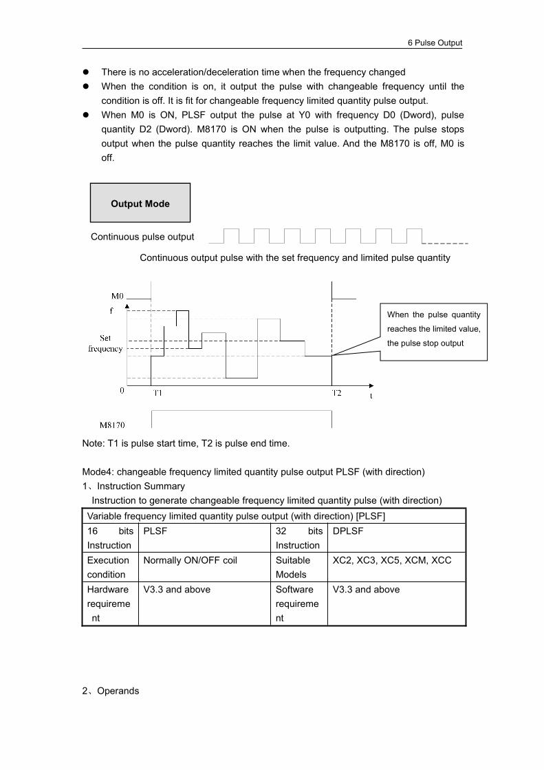
6 Pulse Output
There is no acceleration/deceleration time when the frequency changed When the condition is on, it output the pulse with changeable frequency until the
condition is off. It is fit for changeable frequency limited quantity pulse output. When M0 is ON, PLSF output the pulse at Y0 with frequency D0 (Dword), pulse
quantity D2 (Dword). M8170 is ON when the pulse is outputting. The pulse stopsoutput when the pulse quantity reaches the limit value. And the M8170 is off, M0 isoff.
Continuous output pulse with the set frequency and limited pulse quantity
Note: T1 is pulse start time, T2 is pulse end time.
Mode4: changeable frequency limited quantity pulse output PLSF (with direction)1、Instruction SummaryInstruction to generate changeable frequency limited quantity pulse (with direction)Variable frequency limited quantity pulse output (with direction) [PLSF]16 bitsInstruction
PLSF 32 bitsInstruction
DPLSF
Executioncondition
Normally ON/OFF coil SuitableModels
XC2, XC3, XC5, XCM, XCC
Hardwarerequirement
V3.3 and above Softwarerequirement
V3.3 and above
2、Operands
Continuous pulse output
Output Mode
When the pulse quantity
reaches the limited value,
the pulse stop output
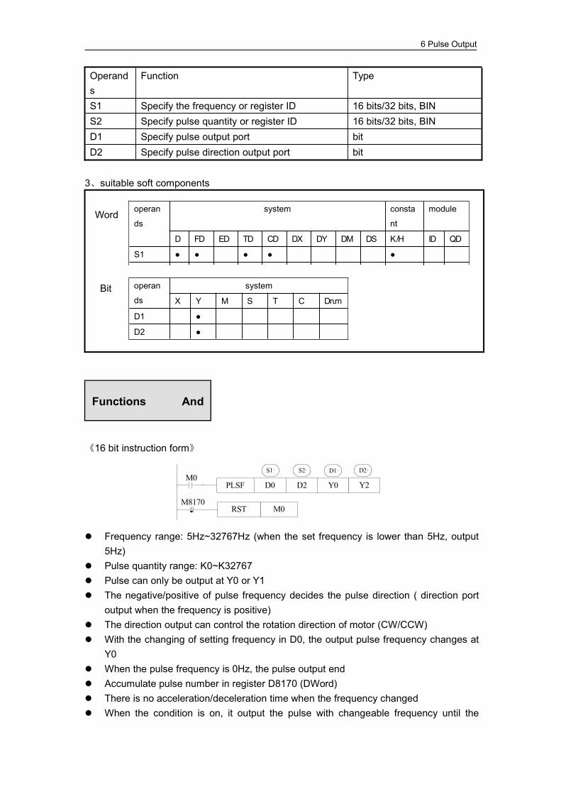
6 Pulse Output
Operands
Function Type
S1 Specify the frequency or register ID 16 bits/32 bits, BINS2 Specify pulse quantity or register ID 16 bits/32 bits, BIND1 Specify pulse output port bitD2 Specify pulse direction output port bit
3、suitable soft components
《16 bit instruction form》
PLSF D0 D2M0
S1· S2·
Y0
D1·
M8170RST M0
Y2
D2·
Frequency range: 5Hz~32767Hz (when the set frequency is lower than 5Hz, output5Hz)
Pulse quantity range: K0~K32767 Pulse can only be output at Y0 or Y1 The negative/positive of pulse frequency decides the pulse direction ( direction port
output when the frequency is positive) The direction output can control the rotation direction of motor (CW/CCW) With the changing of setting frequency in D0, the output pulse frequency changes at
Y0 When the pulse frequency is 0Hz, the pulse output end Accumulate pulse number in register D8170 (DWord) There is no acceleration/deceleration time when the frequency changed When the condition is on, it output the pulse with changeable frequency until the
operan
ds
system consta
nt
module
D FD ED TD CD DX DY DM DS K/H ID QD
S1 ● ● ● ● ●
S2 ● ● ● ● ●
Word
operan
ds
system
X Y M S T C Dn.m
D1 ●
D2 ●
Bit
Functions And

6 Pulse Output
condition is off. It is fit for changeable frequency limited quantity pulse output. When M0 is ON, PLSF output the pulse at Y0 with frequency D0 (word), pulse
quantity D2 (word). M8170 is ON when the pulse is outputting. The pulse stops outputwhen the pulse quantity reaches the limit value. And the M8170 is off, M0 is off.
《32 bit instruction form》
DPLSF D0 D2M0
S1· S2·
Y0
D1·
M8170RST M0
Y2
D2·
Frequency range: 5Hz~200KHz (when the set frequency is lower than 5Hz, output5Hz)
Pulse quantity range: K0~K2147483647 Pulse can only be output at Y0 or Y1 With the changing of setting frequency in D0, the output pulse frequency changes at
Y0 When the pulse frequency is 0Hz, the pulse output end Accumulate pulse number in register D8170 (DWord) There is no acceleration/deceleration time when the frequency changed When the condition is on, it output the pulse with changeable frequency until the
condition is off. It is fit for changeable frequency limited quantity pulse output. When M0 is ON, PLSF output the pulse at Y0 with frequency D0 (Dword), pulse
quantity D2 (Dword). M8170 is ON when the pulse is outputting. The pulse stopsoutput when the pulse quantity reaches the limit value. And the M8170 is off, M0 isoff.
Continuous output pulse with the set frequency and limited pulse quantity
Continuous pulse output
Output Mode
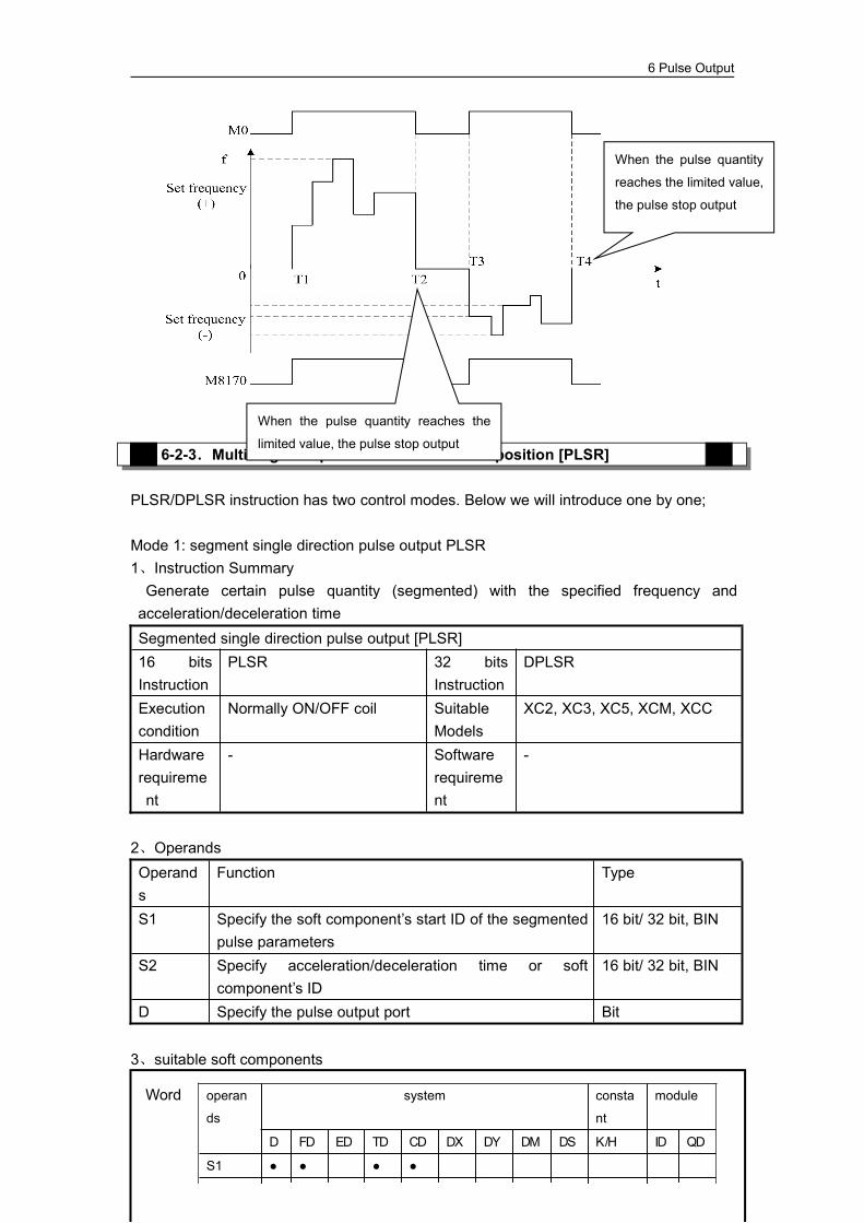
6 Pulse Output
6-2-3.Multi-segment pulse control at relative position [PLSR]
PLSR/DPLSR instruction has two control modes. Below we will introduce one by one;
Mode 1: segment single direction pulse output PLSR1、Instruction SummaryGenerate certain pulse quantity (segmented) with the specified frequency andacceleration/deceleration timeSegmented single direction pulse output [PLSR]16 bitsInstruction
PLSR 32 bitsInstruction
DPLSR
Executioncondition
Normally ON/OFF coil SuitableModels
XC2, XC3, XC5, XCM, XCC
Hardwarerequirement
- Softwarerequirement
-
2、OperandsOperands
Function Type
S1 Specify the soft component’s start ID of the segmentedpulse parameters
16 bit/ 32 bit, BIN
S2 Specify acceleration/deceleration time or softcomponent’s ID
16 bit/ 32 bit, BIN
D Specify the pulse output port Bit
3、suitable soft components
operan
ds
system consta
nt
module
D FD ED TD CD DX DY DM DS K/H ID QD
S1 ● ● ● ●
S2 ● ● ● ● ●
Word
When the pulse quantity
reaches the limited value,
the pulse stop output
When the pulse quantity reaches the
limited value, the pulse stop output

6 Pulse Output
《16 bit instruction form》
PLSR D0 D100 Y0
RST M0
M0
M8170
S1· S2· D·
《32 bit instruction form》
DPLSR D0 D100 Y0
RST M0
M0
M8170
S1· S2· D·
operan
ds
system
X Y M S T C Dn.m
D ●
Bit
Functions and
The parameters’ address is a section starts from Dn or FDn. In the above example(16bit instruction form): D0 set the first segment pulse’s highest frequency, D1 set thefirst segment’s pulse number, D2 set the second segment pulse’s highest frequency,D3 set the second segment’s pulse number, …… if the set value in Dn, Dn+1 is 0,this represents the end of segment, the segment number is not limited.
For 32 bit instruction DPLSR, D0, D1 set the first segment pulse’s highest frequency,D2, D3 set the first segment’s pulse number, D4, D5 set the second segment pulse’shighest frequency, D6, D7 set the second segment’s pulse number……
Acceleration/deceleration time is the time from the start to the first segment’s highestfrequency. Meantime, it defines the slope of all segment’s frequency to time. In thisway the following acceleration/deceleration will perform according to this slope.
Pulse can be output at only Y000 or Y001 Frequency range: 0~32767Hz (16 bits instruction), 0~200KHz (32 bits instruction) Acceleration/deceleration time : 0~65535 ms
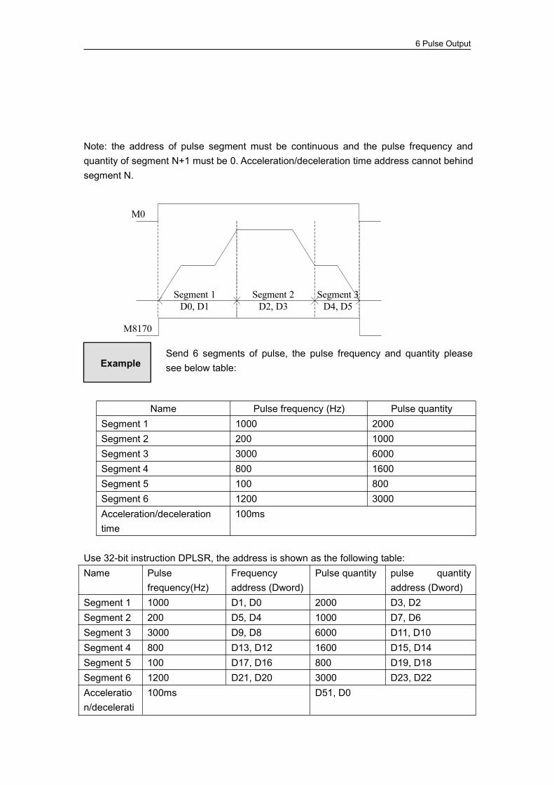
6 Pulse Output
Note: the address of pulse segment must be continuous and the pulse frequency andquantity of segment N+1 must be 0. Acceleration/deceleration time address cannot behindsegment N.
M8170
M0
Segment 1D0, D1
Segment 2D2, D3
Segment 3D4, D5
Name Pulse frequency (Hz) Pulse quantitySegment 1 1000 2000Segment 2 200 1000Segment 3 3000 6000Segment 4 800 1600Segment 5 100 800Segment 6 1200 3000Acceleration/decelerationtime
100ms
Use 32-bit instruction DPLSR, the address is shown as the following table:Name Pulse
frequency(Hz)Frequencyaddress (Dword)
Pulse quantity pulse quantityaddress (Dword)
Segment 1 1000 D1, D0 2000 D3, D2Segment 2 200 D5, D4 1000 D7, D6Segment 3 3000 D9, D8 6000 D11, D10Segment 4 800 D13, D12 1600 D15, D14Segment 5 100 D17, D16 800 D19, D18Segment 6 1200 D21, D20 3000 D23, D22Acceleration/decelerati
100ms D51, D0
ExampleSend 6 segments of pulse, the pulse frequency and quantity pleasesee below table:
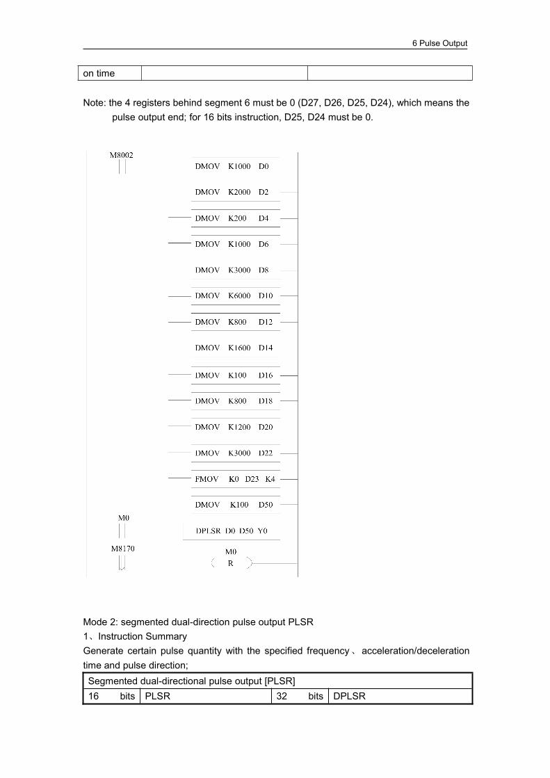
6 Pulse Output
on time
Note: the 4 registers behind segment 6 must be 0 (D27, D26, D25, D24), which means thepulse output end; for 16 bits instruction, D25, D24 must be 0.
Mode 2: segmented dual-direction pulse output PLSR1、Instruction SummaryGenerate certain pulse quantity with the specified frequency、acceleration/decelerationtime and pulse direction;Segmented dual-directional pulse output [PLSR]16 bits PLSR 32 bits DPLSR
6 Pulse Output
Instruction InstructionExecutioncondition
Normally ON/OFF coil SuitableModels
XC2, XC3, XC5, XCM, XCC
Hardwarerequirement
- Softwarerequirement
-
2、OperandsOperands
Function Type
S1 Specify the soft component’s start ID of the segmentedpulse parameters
16 bit/ 32 bit,BIN
S2 Specify acceleration/deceleration time or softcomponent’s ID
16 bit/ 32 bit,BIN
D1 Specify the pulse output port BitD2 Specify the pulse output direction’s port Bit
3、suitable soft components
《16 bit instruction form》
PLSR D0 D100 Y0
RST M0
M0
M8170
S1· S2·
Y3
D1· D2·
The parameters’ address is a section starts from Dn or FDn. In the above example:D0 set the first segment pulse’s highest frequency, D1 set the first segment’s pulsenumber,D2 set the second segment pulse’s highest frequency, D3 set the secondsegment’s pulse number, …… if the set value in Dn, Dn+1 is 0, this represents the
operan
ds
system consta
nt
module
D FD ED TD CD DX DY DM DS K/H ID QD
S1 ● ● ● ●
S2 ● ● ● ● K
Word
operan
ds
system
X Y M S T C Dn.m
D1 ●
D2 ●
Bit
Functions And

6 Pulse Output
end of segment, the segment number is not limited. For 32 bit instruction DPLSR, D0, D1 set the first segment pulse’s highest frequency,
D2, D3 set the first segment’s pulse number, D4, D5 set the second segment pulse’shighest frequency, D6, D7 set the second segment’s pulse number……
Acceleration/deceleration time is the time from the start to the first segment’s highestfrequency. Meantime, it defines the slope of all segment’s frequency to time. In thisway the following acceleration/deceleration will perform according to this slope.
Pulse can be output at only Y0 or Y1 Pulse direction output terminal Y can be specified freely. E.g.: if in S1 (the first
segment) the pulse number is positive, Y output is ON; if the pulse number is negative,Y output is OFF; Note: the pulse direction is decided by the pulse number’s nature(positive or negative) of the first segment.
Frequency range: 0~32767Hz (16 bits), 0~200KHz (32 bits) Pulse number range: 0~K32,767 (16 bits instruction), 0~K2,147,483,647 (32 bits
instruction) Acceleration/deceleration time : below 65535 ms
M8170
M0
Segment 1D0, D1
Segment 2D2, D3
Segment 3D4, D5
Name Pulse frequency (Hz) Pulse quantitySegment 1 1000 2000Segment 2 200 1000Segment 3 3000 6000Segment 4 800 1600Segment 5 100 800Segment 6 1200 3000Acceleration/deceleration time 100ms
Use 32bits instruction DPLSR, the address is shown as the following table:Name Pulse frequency Frequency Pulse quantity Pulse quantity
Example6 segments pulse output. The pulse frequency and quantity are shownin the following table:
6 Pulse Output
(Hz) address (Dword) address (Dword)Segment 1 1000 D1, D0 2000 D3, D2Segment 2 200 D5, D4 1000 D7, D6Segment 3 3000 D9, D8 6000 D11, D10Segment 4 800 D13, D12 1600 D15, D14Segment 5 100 D17, D16 800 D19, D18Segment 6 1200 D21, D20 3000 D23, D22Acceleration/deceleration time
100ms D51, D0
Note: the 4 registers behind segment 6 must be 0 (D27, D26, D25, D24), which means thepulse output end; for 16 bits instruction, D25, D24 must be 0.

6 Pulse Output
6-2-4.Pulse Segment Switch [PLSNEXT]/ [PLSNT]
1、Instruction SummaryEnter the next segment of pulse output;Pulse segment switch [PLSNEXT]/[PLSNT]
6 Pulse Output
16 bitsInstruction
PLSNEXT/PLSNT 32 bitsInstruction
-
Executioncondition
Rising/falling edge SuitableModels
XC2, XC3, XC5, XCM, XCC
Hardwarerequirement
- Softwarerequirement
-
2、OperandsOperands
Function Type
D Specify the pulse output port Bit
3、suitable soft components
《16 bit instruction form》
Y0PLSNEXTM1
PLSR D0 D100 Y0M0
D
If the pulse output reaches the highest frequency at the current segment, andoutput steadily at this frequency; when M1 changes from OFF to ON, then enterthe next pulse output with the acceleration/deceleration time; (this instruction issuitable for multi-segment pulse output)
Run the instruction within the acceleration/deceleration time is invalid Instruction PLSNT is the same to PLSNEXT
operan
ds
system
X Y M S T C Dn.m
D ●
Bit
Functions And

6 Pulse Output
The object needs to move from A to B to C. The speed of the three segments is different.The position of A, B and C is uncertain. We can use DPLSR and PLSNEXT to make thisprogram. We can use proximity switch in position A, B, C. Connect the proximity to PLCterminal X1, X2, X3. Pulse frequency terminal is Y0, pulse direction terminal is Y2.
Name Pulsefrequency (Hz)
Frequencyaddress(Dword)
Pulsequantity
Pulse quantityaddress (Dword)
Segmentorigin-A
1000 D1, D0 999999999 D3, D2
Segment A-B 3000 D5, D4 999999999 D7, D6Segment B-C 2000 D9, D8 999999999 D11, D10Acceleration/decelerationtime
30ms D31, D30
Note: the pulse quantity should be set to a large value to ensure it can reach the proximityswitch. Please clear the 4 registers behind segment 3. (D15, D14, D13, D12).
-------- the dashed line represents the original pulse output
Example
6 Pulse Output
Diagram:

6 Pulse Output
6-2-5.Pulse Stop [STOP]
1、Instruction SummaryStop pulse output immediately;Pulse stop [STOP]16 bitsInstruction
STOP 32 bitsInstruction
-
Executioncondition
Rising/falling edge SuitableModels
XC2, XC3, XC5, XCM, XCC
Hardwarerequirement
- Softwarerequirement
-
2、OperandsOperands
Function Type
D Specify the port to stop pulse output Bit
3、suitable soft components
《16 bit instruction form》
D0PLSR D100 Y0M0
M1
M8170
STOP Y0
RST M0
D
When M0 changes from OFF to be ON, PLSR output pulse at Y0. D0 specify thefrequency, D1 specify the pulse number, D100 specify the acceleration/decelerationtime; when the output pulse number reaches the set value, stop outputting the pulse;on the rising edge of M1, STOP instruction stops outputting the pulse at Y0;
When STOP works, the pulse will stop at once even the M0 is not off.
operan
ds
system
X Y M S T C Dn.m
D ●
Bit
Functions And

6 Pulse Output
6-2-6.Refresh the pulse number at the port [PLSMV]
1、Instruction SummaryRefresh the pulse number at the port;Refresh the pulse number at the port [PLSMV]16 bitsInstruction
- 32 bitsInstruction
PLSMV
Executioncondition
Normally ON/OFF coil SuitableModels
XC2, XC3, XC5, XCM, XCC
Hardwarerequirement
- Softwarerequirement
-
2、OperandsOperands
Function Type
S Specify the pulse number or soft components’ID
32bit, BIN
D Specify the port to refresh the pulse Bit
3、suitable soft components
operan
ds
system
X Y M S T C Dn.m
D ●
Bit
operan
ds
system consta
nt
module
D FD ED TD CD DX DY DM DS K/H ID QD
S ● ● ● ● ●
Word
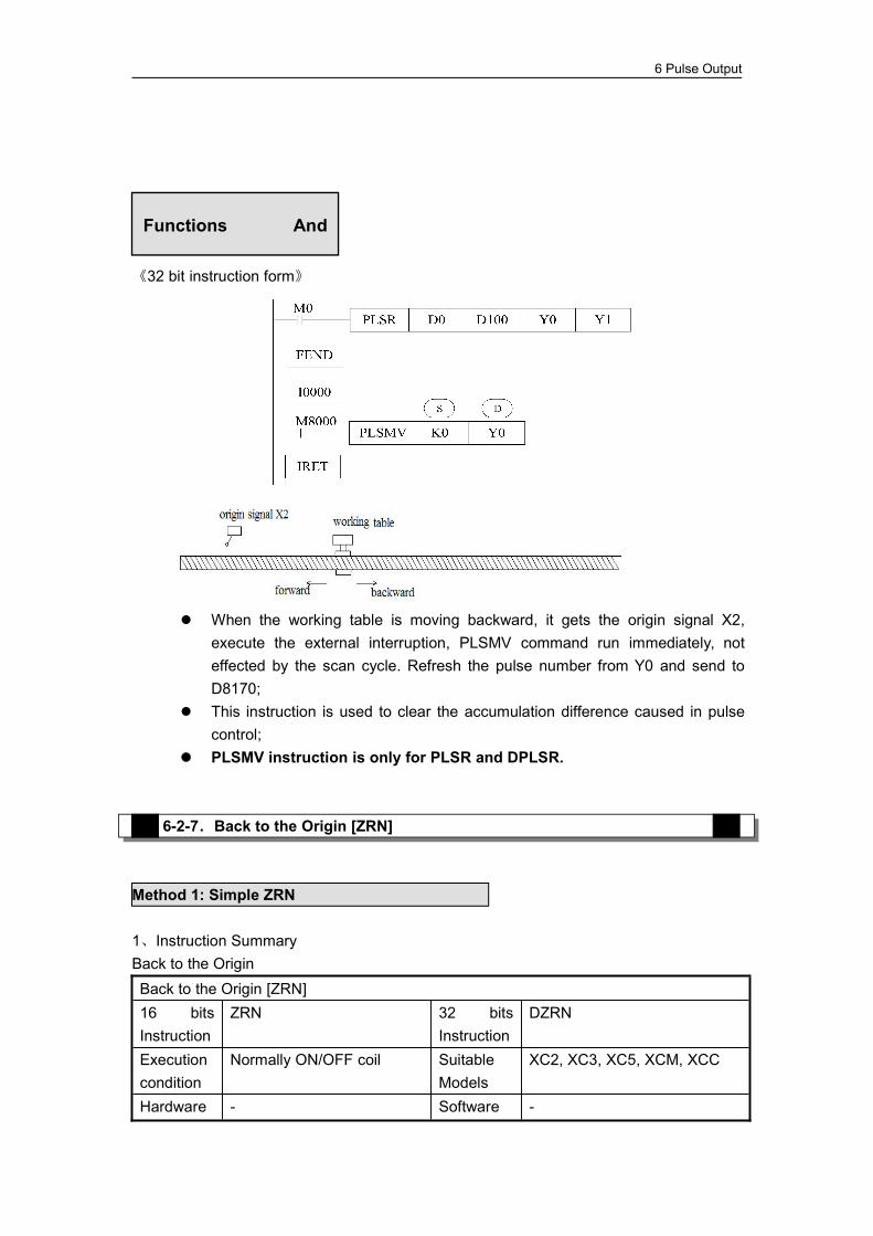
6 Pulse Output
《32 bit instruction form》
When the working table is moving backward, it gets the origin signal X2,execute the external interruption, PLSMV command run immediately, noteffected by the scan cycle. Refresh the pulse number from Y0 and send toD8170;
This instruction is used to clear the accumulation difference caused in pulsecontrol;
PLSMV instruction is only for PLSR and DPLSR.
6-2-7.Back to the Origin [ZRN]
Method 1: Simple ZRN
1、Instruction SummaryBack to the OriginBack to the Origin [ZRN]16 bitsInstruction
ZRN 32 bitsInstruction
DZRN
Executioncondition
Normally ON/OFF coil SuitableModels
XC2, XC3, XC5, XCM, XCC
Hardware - Software -
Functions And
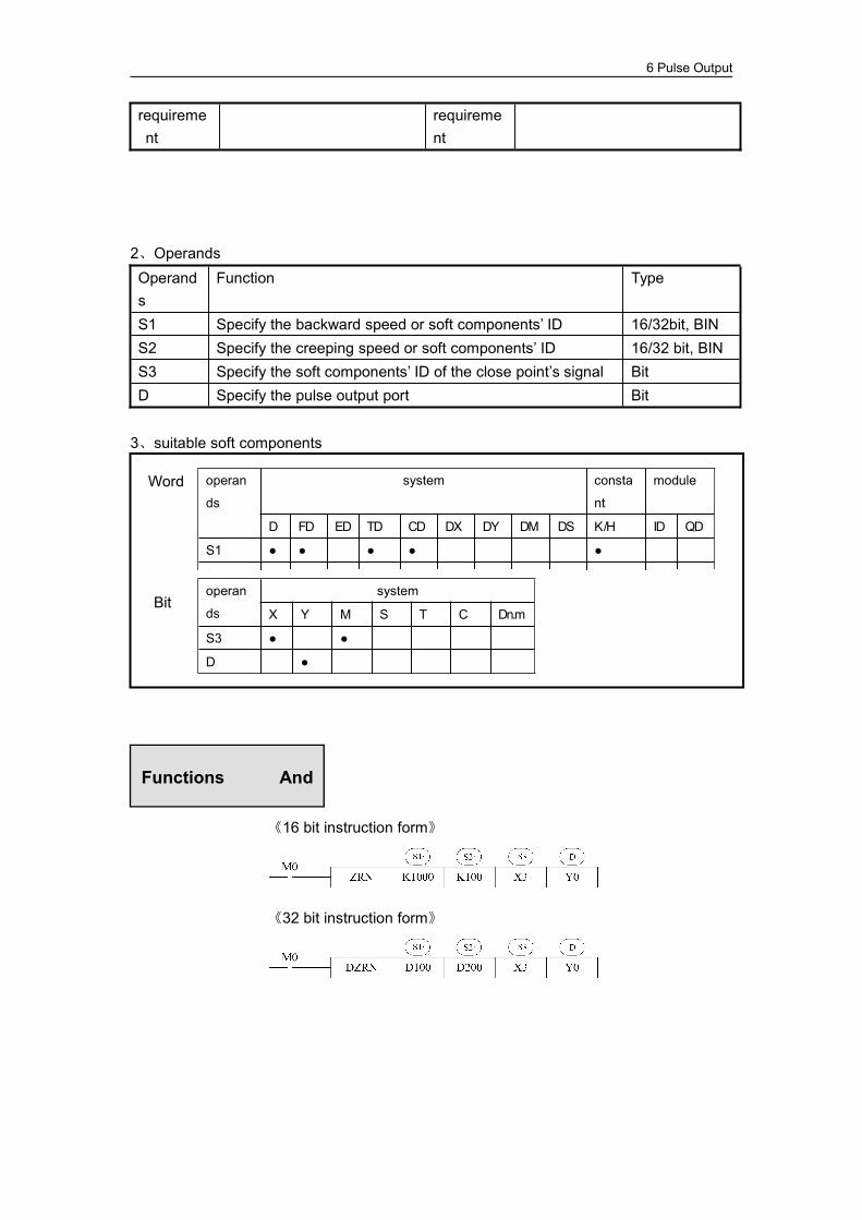
6 Pulse Output
requirement
requirement
2、OperandsOperands
Function Type
S1 Specify the backward speed or soft components’ ID 16/32bit, BINS2 Specify the creeping speed or soft components’ ID 16/32 bit, BINS3 Specify the soft components’ ID of the close point’s signal BitD Specify the pulse output port Bit
3、suitable soft components
《16 bit instruction form》
《32 bit instruction form》
operan
ds
system
X Y M S T C Dn.m
S3 ● ●
D ●
Word
Functions And
Bit
operan
ds
system consta
nt
module
D FD ED TD CD DX DY DM DS K/H ID QD
S1 ● ● ● ● ●
S2 ● ● ● ● ●
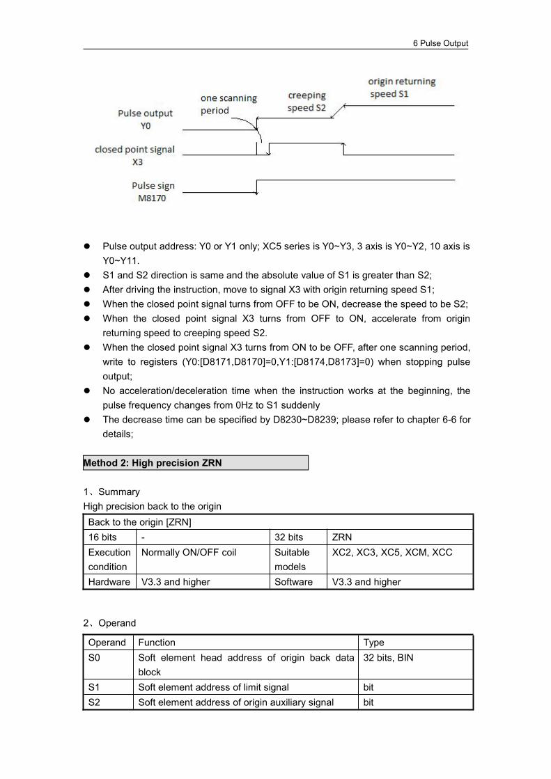
6 Pulse Output
Pulse output address: Y0 or Y1 only; XC5 series is Y0~Y3, 3 axis is Y0~Y2, 10 axis isY0~Y11.
S1 and S2 direction is same and the absolute value of S1 is greater than S2; After driving the instruction, move to signal X3 with origin returning speed S1; When the closed point signal turns from OFF to be ON, decrease the speed to be S2; When the closed point signal X3 turns from OFF to ON, accelerate from origin
returning speed to creeping speed S2. When the closed point signal X3 turns from ON to be OFF, after one scanning period,
write to registers (Y0:[D8171,D8170]=0,Y1:[D8174,D8173]=0) when stopping pulseoutput;
No acceleration/deceleration time when the instruction works at the beginning, thepulse frequency changes from 0Hz to S1 suddenly
The decrease time can be specified by D8230~D8239; please refer to chapter 6-6 fordetails;
Method 2: High precision ZRN
1、SummaryHigh precision back to the originBack to the origin [ZRN]16 bits - 32 bits ZRNExecutioncondition
Normally ON/OFF coil Suitablemodels
XC2, XC3, XC5, XCM, XCC
Hardware V3.3 and higher Software V3.3 and higher
2、Operand
Operand Function TypeS0 Soft element head address of origin back data
block32 bits, BIN
S1 Soft element address of limit signal bitS2 Soft element address of origin auxiliary signal bit
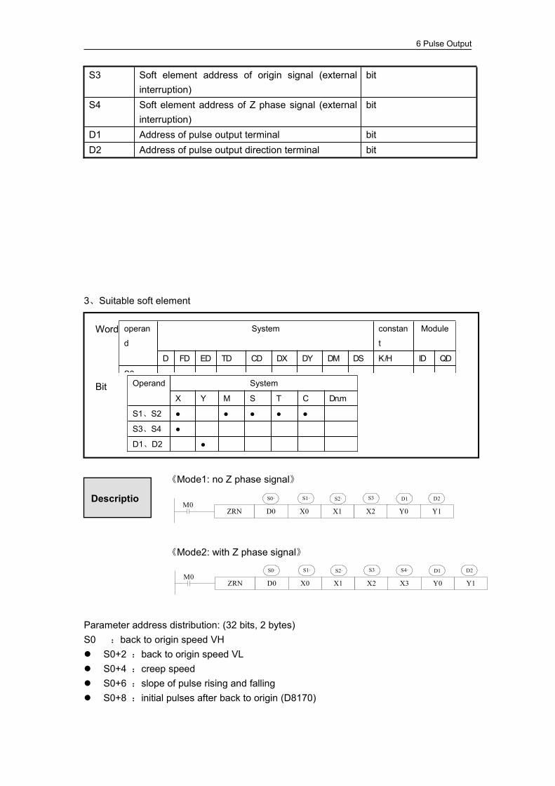
6 Pulse Output
S3 Soft element address of origin signal (externalinterruption)
bit
S4 Soft element address of Z phase signal (externalinterruption)
bit
D1 Address of pulse output terminal bitD2 Address of pulse output direction terminal bit
3、Suitable soft element
《Mode1: no Z phase signal》
《Mode2: with Z phase signal》
Parameter address distribution: (32 bits, 2 bytes)S0 :back to origin speed VH S0+2 :back to origin speed VL S0+4 :creep speed S0+6 :slope of pulse rising and falling S0+8 :initial pulses after back to origin (D8170)
Operand System
X Y M S T C Dn.m
S1、S2 ● ● ● ● ●
S3、S4 ●
D1、D2 ●
Word
Descriptio
Bit
operan
d
System constan
t
Module
D FD ED TD CD DX DY DM DS K/H ID QD
S0 ● ● ● ●
ZRN D0 X0 X1M0
S2·
X2
S3S0·
Y0 Y1
D1 D2S1·
ZRN D0 X0 X1M0
S2·
X2
S3S0·
X3 Y0
D1 D2S1·
Y1
S4·

6 Pulse Output
S0+10:Z phase count value (for mode2)
(A)back start point is behind the originMode1:
Description: Move towards the origin with speed VH. If it encounters origin auxiliary signal S2, it will decelerate to speed VL with the slope
K (note: if it encounters the origin when decelerating from VH to VL, please modifythe pulse slope or origin position to avoid it).
Keep forward with the current speed VL. Decelerate to 0 with the slope K after touching the origin. Start to delay (delay time is FD8209, unit is ms). It accelerates to creep speed with
the slope K after delaying. Move in reverse direction with creep speed. Stop origin returning when it leaves the origin with creep speed.
Change the pulses (D8170) to setting value.
Note: in this mode, please keep the origin limit switch ON during the process (fromtouching the origin limit switch at speed VL to stop origin returning)
Mode2:
VL
Slope
VH
Speed=0
Limit Origin Origin auxiliary
Creep speed

6 Pulse Output
VL
Slope VH
Speed=0
Limit Origin Origin auxiliary
Creep speed
Count for Z phase signal
Description: Move towards origin with speed VH. If it encounters origin auxiliary signal S2, decelerate to speed VL with slope K. Move forward at speed VL. Decelerate to 0 with slope K when encountering the origin. Start to delay (the delay time is FD8209, unit is ms). Accelerate to creep speed with
the slope K. Move in reverse direction at creep speed. Stop Z phase counting when leaving the origin at creep speed. Stop origin returning when Z phase cumulative value is equal to setting value.
Change the pulses (D8170) to setting value.
Note: in this mode, please keep the origin limit switch ON during the process (fromtouching the origin limit switch at speed VL to stop origin returning)
(B)the start point is ahead the origin, with limit signal
Mode1:
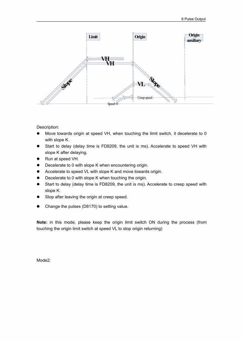
6 Pulse Output
VLSlope
VH
Speed=0
Limit Origin Origin auxiliary
Creep speed
VH
Slope
Description: Move towards origin at speed VH, when touching the limit switch, it decelerate to 0
with slope K. Start to delay (delay time is FD8209, the unit is ms). Accelerate to speed VH with
slope K after delaying. Run at speed VH. Decelerate to 0 with slope K when encountering origin. Accelerate to speed VL with slope K and move towards origin. Decelerate to 0 with slope K when touching the origin. Start to delay (delay time is FD8209, the unit is ms). Accelerate to creep speed with
slope K. Stop after leaving the origin at creep speed.
Change the pulses (D8170) to setting value.
Note: in this mode, please keep the origin limit switch ON during the process (fromtouching the origin limit switch at speed VL to stop origin returning)
Mode2:

6 Pulse Output
VLSlope
VH
Speed=0
Limit Origin Origin auxiliary
Creep speed
VH
Slope
Count for Z phase signal
Description: Move towards origin at speed VH, decelerate to 0 with slope K when touching the
limit signal. Start to delay (delay time is FD8209, the unit is ms). Accelerate to speed VH with
slope K after delaying. Run at speed VH. Decelerate to 0 with slope K when encountering the origin. Accelerate to speed VL with slope K and move toward origin. Decelerate to 0 with slope K when touching the origin. Start to delay (delay time is FD8209, the unit is ms). Accelerate to creep speed with
slope K after delaying. Start to count Z phase signal after leaving origin at creep speed. Stop origin returning when cumulative value of Z phase signal is equal to setting
value. Change the pulses to setting value. (D8170)
Note: in this mode, please keep the origin limit switch ON during the process (fromtouching the origin limit switch at speed VL to stop origin returning)
6-2-8.Relative position single-segment pulse control [DRVI]
1、Instruction SummaryRelative position single-segment pulse control;Relative position single-segment pulse control [DRVI]16 bitsInstruction
DRVI 32 bitsInstruction
DDRVI
Executioncondition
Normally ON/OFF coil SuitableModels
XC2, XC3, XC5, XCM, XCC

6 Pulse Output
Hardwarerequirement
- Softwarerequirement
-
2、OperandsOperands
Function Type
S1 Specify the output pulse value or soft components ID 16/32bit, BINS2 Specify the output pulse frequency or soft
components ID16/32 bit, BIN
D1 Specify the pulse output port BitD2 Specify the pulse output direction port Bit
3、suitable soft components
《16 bit instruction form》
《32 bit instruction form》
operan
ds
system
X Y M S T C Dn.m
D1 ●
D2 ●
Word
Functions And
Bit
operan
ds
system consta
nt
module
D FD ED TD CD DX DY DM DS K/H ID QD
S1 ● ● ● ● ●
S2 ● ● ● ● ●

6 Pulse Output
Pulse output ID: only Y0 or Y1; XC5 series is Y0~Y3, 3 axis is Y0~Y2, 10 axis isY0~Y11
Pulse output direction can specify any Y; Acceleration/deceleration time is specified by D8230 (single word) The relative drive form means: move from the current position (the distance from
current position to target position); Confirm the value of current position registers before executing the instruction
(D8171, D8170[Y0]/ D8174, D8173[Y1] ……)
The current position of X axis is (100, 0), it will move to target position (3000, 0) at thespeed of 1000Hz, pulse output terminal is Y0, direction terminal is Y4. The distancebetween current position and target position is 2900=3000-100. The DRVI executingdiagram is shown as below:
Program:
Example

6 Pulse Output
6-2-9.Absolute position single-segment pulse control [DRVA]
1、Instruction SummaryAbsolute position single-segment pulse controlAbsolute position single-segment pulse control [DRVA]16 bitsInstruction
DRVA 32 bitsInstruction
DDRVA
Executioncondition
Normally ON/OFF coil SuitableModels
XC2, XC3, XC5, XCM, XCC
Hardwarerequirement
- Softwarerequirement
-
2、OperandsOperands
Function Type
S1 Specify the output pulse value or soft components ID 16/32bit, BINS2 Specify the output pulse frequency or soft components ID 16/32 bit, BIND1 Specify the pulse output port BitD2 Specify the pulse output direction port Bit
3、suitable soft components
《16 bit instruction form》
operan
ds
system
X Y M S T C Dn.m
D1 ●
D2 ●
Word
Functions And
Bit
operan
ds
system consta
nt
module
D FD ED TD CD DX DY DM DS K/H ID QD
S1 ● ● ● ● ●
S2 ● ● ● ● ●
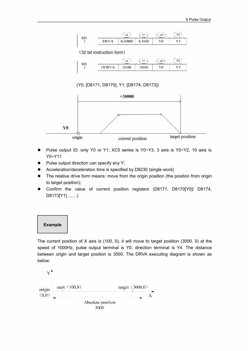
6 Pulse Output
《32 bit instruction form》
(Y0: [D8171, D8170], Y1: [D8174, D8173])
Pulse output ID: only Y0 or Y1; XC5 series is Y0~Y3, 3 axis is Y0~Y2, 10 axis isY0~Y11
Pulse output direction can specify any Y; Acceleration/deceleration time is specified by D8230 (single word) The relative drive form means: move from the origin position (the position from origin
to target position); Confirm the value of current position registers (D8171, D8170[Y0]/ D8174,
D8173[Y1] ……)
The current position of X axis is (100, 0), it will move to target position (3000, 0) at thespeed of 1000Hz, pulse output terminal is Y0, direction terminal is Y4. The distancebetween origin and target position is 3000. The DRVA executing diagram is shown asbelow:
Example
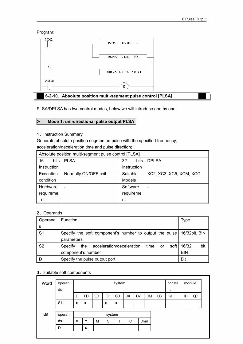
6 Pulse Output
Program:
6-2-10.Absolute position multi-segment pulse control [PLSA]
PLSA/DPLSA has two control modes, below we will introduce one by one;
Mode 1: uni-directional pulse output PLSA
1、Instruction SummaryGenerate absolute position segmented pulse with the specified frequency,acceleration/deceleration time and pulse direction;Absolute position multi-segment pulse control [PLSA]16 bitsInstruction
PLSA 32 bitsInstruction
DPLSA
Executioncondition
Normally ON/OFF coil SuitableModels
XC2, XC3, XC5, XCM, XCC
Hardwarerequirement
- Softwarerequirement
-
2、OperandsOperands
Function Type
S1 Specify the soft component’s number to output the pulseparameters
16/32bit, BIN
S2 Specify the acceleration/deceleration time or softcomponent’s number
16/32 bit,BIN
D Specify the pulse output port Bit
3、suitable soft components
operan
ds
system
X Y M S T C Dn.m
D1 ●
Word
Bit
operan
ds
system consta
nt
module
D FD ED TD CD DX DY DM DS K/H ID QD
S1 ● ● ● ●
S2 ● ● ● ● K

6 Pulse Output
《16 bit instruction form》
《32 bit instruction form》
The parameters’ address is a section starts from Dn or FDn. In the above example:D0 set the first segment pulse’s highest frequency 、 D1 set the first segment’sabsolute position,D2 set the second segment pulse’s highest frequency、D3 set thesecond segment’s absolute position,…… if the set value in Dn、Dn+1 is 0, thisrepresents the end of segment, we can set 24 segments in total;
For 32 bits instruction DPLSA, D0, D1 set the first segment pulse highest frequency,D2,D3 set the first segment pulse quantity, D4, D5 set the second segment pulsehighest frequency, D6,D7 set the second segment pulse quantity……. If the settingvalue of Dn, Dn+1, Dn+2, Dn+3 are 0, it means the end of the segment. It can set 24segments in total.
Acceleration/deceleration time is the time from the start to the first segment’s highestfrequency. Meantime, it defines the slope of all segment’s frequency to time. In thisway the following acceleration/deceleration will perform according to this slope.
Pulse can be output at only Y0 or Y1; XC5 series is Y0~Y3, 3 axis is Y0~Y2, 10 axisis Y0~Y11;
Functions And

6 Pulse Output
Frequency range: 0~32767Hz (16 bits instruction), 0~200KHz (32 bits instruction) Pulse number range: K0~K32,767 (16 bits instruction), K0~K2,147,483,647 (32 bits
instruction) Confirm the value in current position registers (D8171, D8170[Y0]/ D8174,
D8173[Y1] ……)
Note: if the segment quantity is n, the address of the segments must be continuous, andthe pulse frequency and quantity of n+1 segment must be 0. It means the pulse outputend. The address of acceleration/deceleration time cannot follow the segment n.
Output 6 segments of pulse through instruction DPLSA. Y0 is pulse output terminal.
Name Frequency (Hz) Absolution positionSegment 1 1000 2000Segment 2 200 3000Segment 3 3000 9000Segment 4 800 10600Segment 5 100 11400Segment 6 1200 14400Acceleration/deceleration time 100ms
Use 32 bits instruction DPLSA:Name Frequency
(Hz)Frequencyaddress(Dword)
Absolutionposition
Absolution positionaddress (Dword)
Segment 1 1000 D1、D0 2000 D3、D2Segment 2 200 D5、D4 3000 D7、D6Segment 3 3000 D9、D8 9000 D11、D10Segment 4 800 D13、D12 10600 D15、D14Segment 5 100 D17、D16 11400 D19、D18Segment 6 1200 D21、D20 14400 D23、D22Acceleration/deceleration time
100ms D51、D0
Note: the 4 registers after segment 6 must be 0. (D27, D26, D25, D24).It means the pulseoutput end. For 16 bits instruction PLSA, 2 registers after segment 6 must be 0.
Example
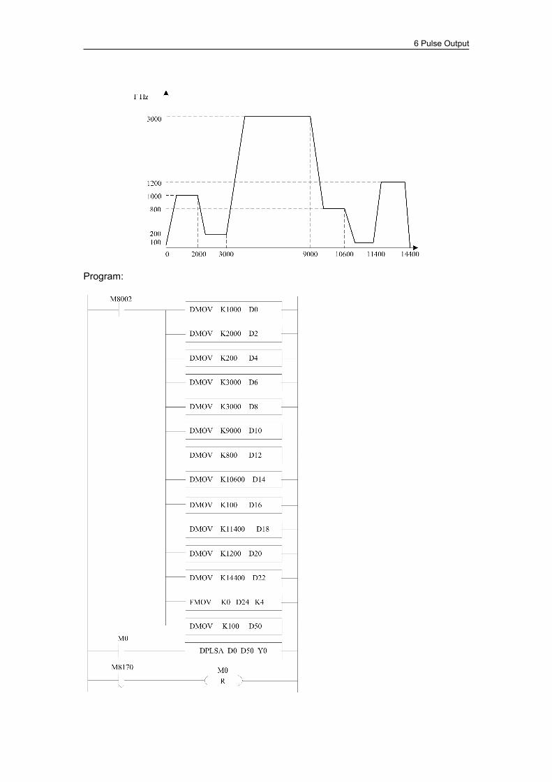
6 Pulse Output
Program:

6 Pulse Output
Mode2: dual-directional pulse output PLSA
1、Instruction SummaryGenerate absolute position pulse with the specified frequency, acceleration/decelerationtime and pulse direction;Absolute position multi-segment pulse control [PLSA]16 bitsInstruction
PLSA 32 bitsInstruction
DPLSA
Executioncondition
Normally ON/OFF coil SuitableModels
XC2, XC3, XC5, XCM, XCC
Hardwarerequirement
- Softwarerequirement
-
2、OperandsOperands
Function Type
S1 Specify the soft component’s number to output the pulseparameters
16/32bit, BIN
S2 Specify the acceleration/deceleration time or softcomponent’s number
16/32 bit, BIN
D1 Specify the pulse output port BitD2 Specify the pulse direction port Bit
3、suitable soft components
《16 bit instruction form》
operan
ds
system
X Y M S T C Dn.m
D1 ●
D2 ●
Word
Functions And Actions
Bit
operan
ds
system consta
nt
module
D FD ED TD CD DX DY DM DS K/H ID QD
S1 ● ● ● ●
S2 ● ● ● ● K
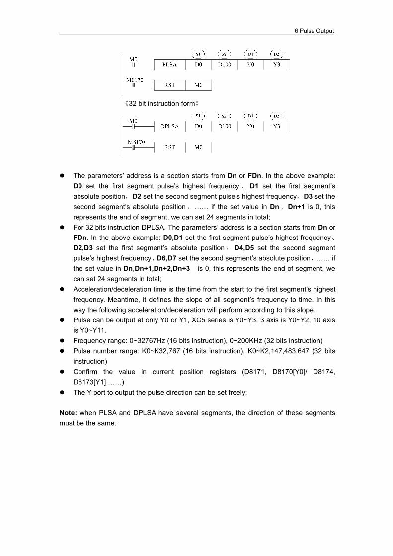
6 Pulse Output
《32 bit instruction form》
The parameters’ address is a section starts from Dn or FDn. In the above example:D0 set the first segment pulse’s highest frequency 、 D1 set the first segment’sabsolute position,D2 set the second segment pulse’s highest frequency、D3 set thesecond segment’s absolute position,…… if the set value in Dn、Dn+1 is 0, thisrepresents the end of segment, we can set 24 segments in total;
For 32 bits instruction DPLSA. The parameters’ address is a section starts from Dn orFDn. In the above example: D0,D1 set the first segment pulse’s highest frequency、D2,D3 set the first segment’s absolute position,D4,D5 set the second segmentpulse’s highest frequency、D6,D7 set the second segment’s absolute position,…… ifthe set value in Dn,Dn+1,Dn+2,Dn+3 is 0, this represents the end of segment, wecan set 24 segments in total;
Acceleration/deceleration time is the time from the start to the first segment’s highestfrequency. Meantime, it defines the slope of all segment’s frequency to time. In thisway the following acceleration/deceleration will perform according to this slope.
Pulse can be output at only Y0 or Y1, XC5 series is Y0~Y3, 3 axis is Y0~Y2, 10 axisis Y0~Y11.
Frequency range: 0~32767Hz (16 bits instruction), 0~200KHz (32 bits instruction) Pulse number range: K0~K32,767 (16 bits instruction), K0~K2,147,483,647 (32 bits
instruction) Confirm the value in current position registers (D8171, D8170[Y0]/ D8174,
D8173[Y1] ……) The Y port to output the pulse direction can be set freely;
Note: when PLSA and DPLSA have several segments, the direction of these segmentsmust be the same.
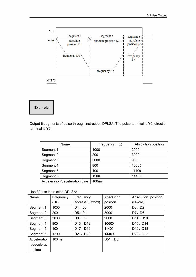
6 Pulse Output
Output 6 segments of pulse through instruction DPLSA. The pulse terminal is Y0, directionterminal is Y2.
Name Frequency (Hz) Absolution positionSegment 1 1000 2000Segment 2 200 3000Segment 3 3000 9000Segment 4 800 10600Segment 5 100 11400Segment 6 1200 14400Acceleration/deceleration time 100ms
Use 32 bits instruction DPLSA:Name Frequency
(Hz)Frequencyaddress (Dword)
Absolutionposition
Absolution position(Dword)
Segment 1 1000 D1、D0 2000 D3、D2Segment 2 200 D5、D4 3000 D7、D6Segment 3 3000 D9、D8 9000 D11、D10Segment 4 800 D13、D12 10600 D15、D14Segment 5 100 D17、D16 11400 D19、D18Segment 6 1200 D21、D20 14400 D23、D22Acceleration/deceleration time
100ms D51、D0
Example
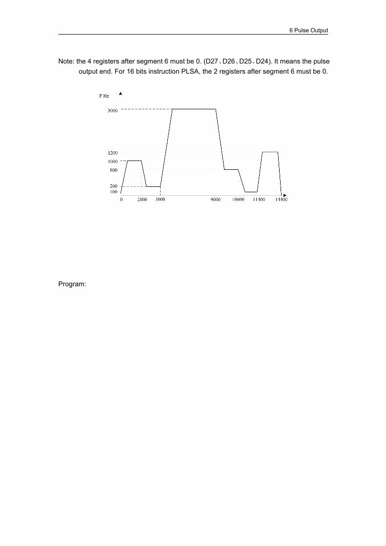
6 Pulse Output
Note: the 4 registers after segment 6 must be 0. (D27、D26、D25、D24). It means the pulseoutput end. For 16 bits instruction PLSA, the 2 registers after segment 6 must be 0.
Program:

6 Pulse Output
6-2-11.Relative position multi-section pulse control [PTO]
1、SummaryProduce relative position multi-section pulse as setting parameters.Relative position multi-section pulse control [PTO]16 bits - 32 bits PTOExecutioncondition
Edge triggering Suitablemodels
XC3、XC5、XCM、XCC
Hardware V3.3 and higher Software V3.3 and higher
2、OperandOperands
Function Type
S1 Soft element head address of output pulseparameters
32 bits, BIN
S2 External interruption input port no. Bit

6 Pulse Output
D1 Pulse output port no. BitD2 Pulse output direction port no. Bit
3、Suitable soft element
PTO instruction has two control modes.
Mode1: PTO without external interruption
《32 bits instruction》
《no direction》
《with direction》
Parameters distribution: (the parameters are 32 bits 2 bytes): S1 :section quantity N, range 1~255 S1+2 :reserved S1+4 :pulse direction, 0 is positive direction; 1 is negative direction
Among each section, only one section pulse quantity can be 0. S1+6 :Pulse falling slope, which is decreasing frequency per second. 0 means
urgent stop.
S1+8 :start frequency of section 1 S1+10:end frequency of section 1 S1+12:pulse quantity of section 1
Oper
-and
System
X Y M S T C Dn.m
S2 ●
D1 ●
D2 ●
Word
Descriptio
Bit
Oper
-and
System Cons
t-ant
Module
D FD ED TD CD DX DY DM DS K/H ID QD
S1 ● ● ●
PTO D0 Y0M0 S1· D1·
PTO D0 Y0M0 S1· D1·
Y1
D2·

6 Pulse Output
S1+14:start frequency of section 2 S1+16:end frequency of section 2 S1+18:pulse quantity of section 2
S1+20:start frequency of section 3 S1+22:end frequency of section 3 S1+24:pulse quantity of section 3
…… and so on, user can set section N parameters
The parameters address starts from Dn or FDnIn the above example:(D1,D0) is pulse section quantity;(D5,D4)is pulse direction;(D7,D6)is pulse falling frequency;(D9,D8)is start frequency of section 1;(D11,D10)is end frequency of section 1; (D13, D12) is the pulse quantity of section 1. The maxsection quantity can be 255.
Pulse output: Y0, Y1; the pulse output terminal is different for each model. If pulse quantity of section m is 0, this means the pulse quantity is unlimited. If pulse quantity of section m is 0, the start frequency must be equal to the end
frequency; otherwise this section will not be executed. If pulse quantity is not 0, the pulse direction is decided by the positive/negative of
pulse. If the pulse quantity is 0, the pulse direction is set through S1+4. S1+6 is the slow stop slope when executing PSTOP (refer to PSTOP instruction). Pulse parameters occupy the register size: [(N*3+4) + (N*3+4) + (N*4+5)]*2. The instruction is executed at the rising edge; if the signal is normally close, the
instruction will be executed repeatedly.
Section Startfrequency
(Hz)
End frequency(Hz)
Relative pulsequantity
1 2 3 4 5 6 7 8 9
ExampleContinuous output 9 sections of pulses, the pulse output terminal is Y0,pulse direction terminal is Y2, the start frequency and end frequencyplease see the following table:
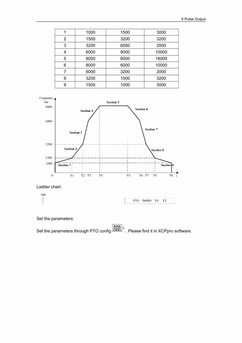
6 Pulse Output
1 1000 1500 30002 1500 3200 32003 3200 6000 20004 6000 8000 100005 8000 8000 180006 8000 6000 100007 6000 3200 20008 3200 1500 32009 1500 1000 3000
Ladder chart:
Set the parameters:
Set the parameters through PTO config . Please find it in XCPpro software.

6 Pulse Output
Note:(1) PTO parameters will occupy the registers of D4000~D4205, please don’t use
these registers for other purpose.
(2) Click “Write to PLC” / OK. Then click stop , run .

6 Pulse Output
Mode2: PTO with external interruption
《32 bits instruction》
Parameter distribution (the parameter is 32 bits, 2 bytes): S1 :section quantity N, range 1~255 S1+2 :reserved S1+4 :pulse direction (the section of 0 pulses), 0 is positive direction, 1 is negative
direction S1+6 :pulse falling slope, decreasing frequency per second, 0 is urgent stop
S1+8 :start frequency of section 1 S1+10:end frequency of section 1 S1+12:pulse quantity of section 1
S1+14:start frequency of section 2 S1+16:end frequency of section 2 S1+18:pulse quantity of section 2
S1+20:start frequency of section 3 S1+22:end frequency of section 3 S1+24:pulse quantity of section 3
…… And so on, user can set the parameters of section N
If user has not set the 0 pulse section, the instruction will not be executed. If the external signal is produced in zero pulse section, it will switch to the next section
(if there is no next section, stop the pulse output). If the external signal is produced in non-zero pulse section, it will run the rest pulses
with the set slope (S1+6 parameter); if the rest pulses is larger than the pulse quantityof frequency falling section, it will run a smooth section and then the falling section.
S1+6 are the urgent stop slope when running PSTOP instruction.
Descriptio
PTO D0 X1M0 S1· D1·
Y0
S2·
1 2 6 7 8
Extenal signal

6 Pulse Output
Cannot support absolute position instruction, cannot support instruction withdirection.
The instruction will be executed at the rising edge; if it is normally close signal, theinstruction will be executed repeatedly.
The instruction execution in different conditions:
The external interruption signal is produced in zero pulse section.
The instruction will switch to the next section when encountering the externalinterruption signal, Ss=S3+S4+S5.S3 is section 3 pulse quantity.S4 is section 4 pulse quantity.S5 is section 5 pulse quantity.
External interruption signal is produced in non-zero pulse section, rest pulses Ss islarger than falling pulses Sn.
When encountering the external interruption signal, it runs the smooth section withthe current frequency Sm=Ss-Sn, then the falling section Sn.
Ss is pulses of rest section.Sn is pulses of frequency falling section when encountering external interruptionsignal.Sm is pulses of smooth section when encountering the external interruption signal.S6 is the pulses of section 6S7 is the pulses of section 7S8 is the pulses of section 8
1 4 5
External signal
S3
4 6 7 8
External signal
Slope KS
nm
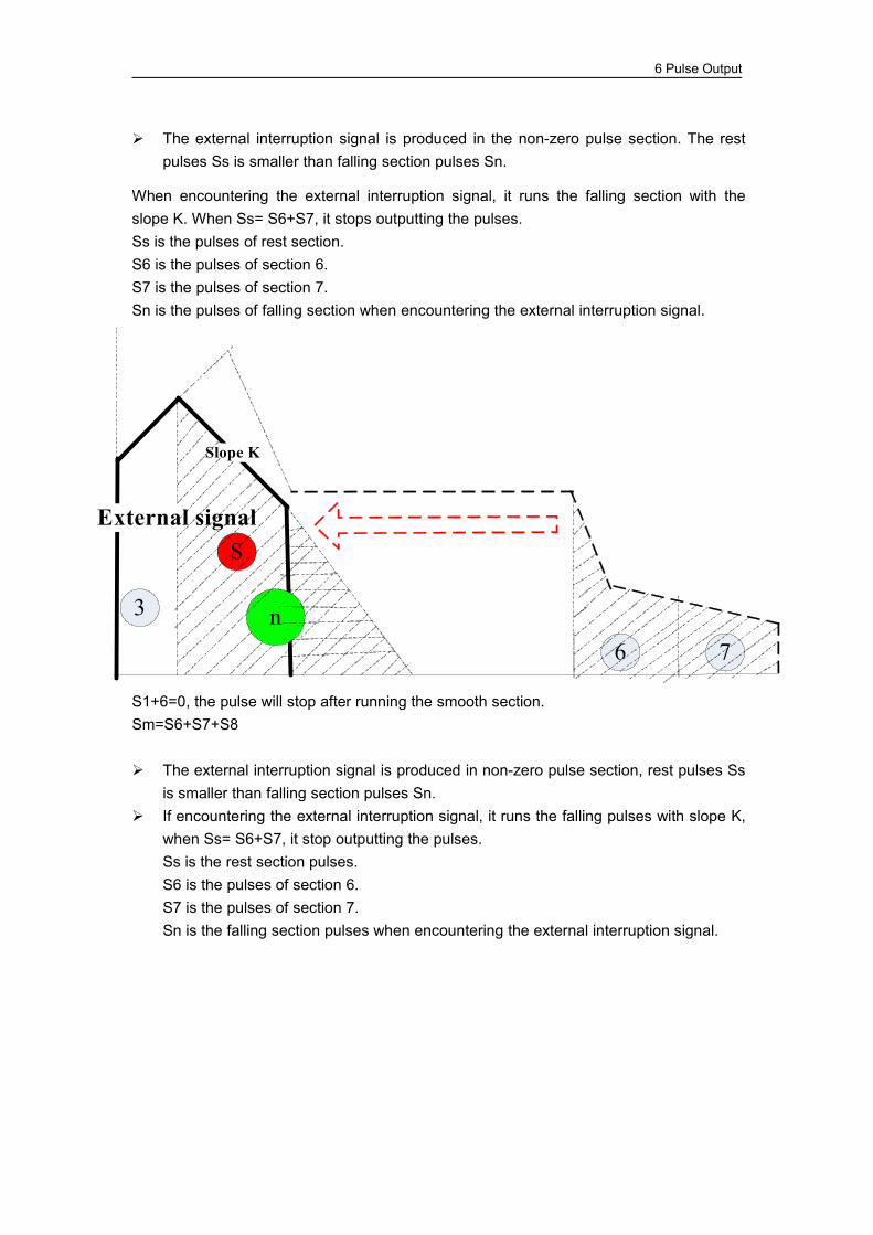
6 Pulse Output
The external interruption signal is produced in the non-zero pulse section. The restpulses Ss is smaller than falling section pulses Sn.
When encountering the external interruption signal, it runs the falling section with theslope K. When Ss= S6+S7, it stops outputting the pulses.Ss is the pulses of rest section.S6 is the pulses of section 6.S7 is the pulses of section 7.Sn is the pulses of falling section when encountering the external interruption signal.
S1+6=0, the pulse will stop after running the smooth section.Sm=S6+S7+S8
The external interruption signal is produced in non-zero pulse section, rest pulses Ssis smaller than falling section pulses Sn.
If encountering the external interruption signal, it runs the falling pulses with slope K,when Ss= S6+S7, it stop outputting the pulses.Ss is the rest section pulses.S6 is the pulses of section 6.S7 is the pulses of section 7.Sn is the falling section pulses when encountering the external interruption signal.
3
6 7
External signal
Slope K
S
n
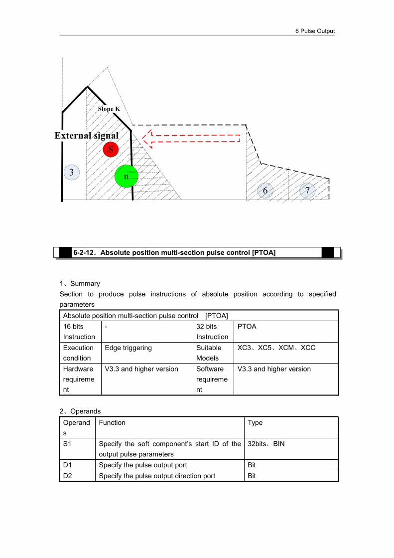
6 Pulse Output
6-2-12.Absolute position multi-section pulse control [PTOA]
1、SummarySection to produce pulse instructions of absolute position according to specifiedparametersAbsolute position multi-section pulse control [PTOA]16 bitsInstruction
- 32 bitsInstruction
PTOA
Executioncondition
Edge triggering SuitableModels
XC3、XC5、XCM、XCC
Hardwarerequirement
V3.3 and higher version Softwarerequirement
V3.3 and higher version
2、OperandsOperands
Function Type
S1 Specify the soft component’s start ID of theoutput pulse parameters
32bits,BIN
D1 Specify the pulse output port BitD2 Specify the pulse output direction port Bit
3
6 7
External signal
Slope K
S
n

6 Pulse Output
3、Suitable soft components
Mode: PTOA (Fixed pulse quantity)
《32 bits instruction form》
《Without direction》
《With direction》
The parameters address and functions are shown as below (the parameter is 32 bits, twobytes): S1 :Total section N, range is 1~255 S1+2 :reserved S1+4 :The direction(0 is positive,1 is negative) of unlimited pulse section (zero pulse
section) S1+6 : Pulse descending slope, decreasing frequency per second, 0 means urgent
stop
S1+8 : Start pulse frequency of section 1 S1+10: End pulse frequency of section 1 S1+12:Absolute pulse position of section 1
S1+14:Start pulse frequency of section 2
operand
s
System
X Y M S T C Dn.m
D1 ●
D2 ●
Word
Bit
operand
s
System constan
t
module
D FD ED TD CD DX DY DM DS K/H ID QD
S1 ● ● ● ●
PTOA D0 Y0M0
S1· D1·
PTOA D0 Y0M0 S1· D1·
Y1
D2·
Description

6 Pulse Output
S1+16:End pulse frequency of section 2 S1+18:Absolute pulse position of section 2
S1+20:Start pulse frequency of section 3 S1+22:End pulse frequency of section 3 S1+24:Absolute pulse position of section 3
…… The pulse parameters address of section N can be known by this discipline
The pulse direction of section 1 is decided by current pulse quantity and cumulativepulse quantity, other section directions are decided by current pulse quantity and lastsection pulse quantity;
Occupied registers size: [(N*3+4)+(N*3+4)+(N*4+5)]*2; The toggle condition to execute the pulse is rising edge, if the signal is closed signal
the pulse will execute repeatedly.
Name Start Frequency(Hz) EndFrequency(Hz)
Absolute pulse quantity of eachsection
Section 1 1000 1500 3000Section 2 1500 3200 6200Section 3 3200 6000 8200Section 4 6000 8000 18200Section 5 8000 8000 36200Section 6 8000 6000 46200Section 7 6000 3200 48200Section 8 3200 1500 51400Section 9 1500 1000 54400
1 2 3 4 5 6 7 8 9
ExampleThe pulse output terminal is Y0, direction terminal is Y2; The start, endfrequency, pulse absolute position is shown in below table:
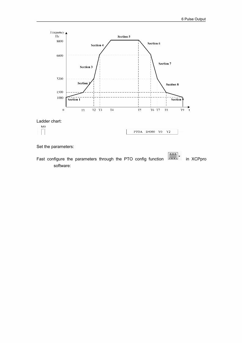
6 Pulse Output
Ladder chart:
Set the parameters:
Fast configure the parameters through the PTO config function in XCPprosoftware:
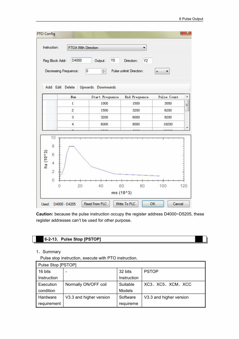
6 Pulse Output
Caution: because the pulse instruction occupy the register address D4000~D5205, theseregister addresses can’t be used for other purpose.
6-2-13.Pulse Stop [PSTOP]
1、SummaryPulse stop instruction, execute with PTO instruction.Pulse Stop [PSTOP]16 bitsInstruction
- 32 bitsInstruction
PSTOP
Executioncondition
Normally ON/OFF coil SuitableModels
XC3、XC5、XCM、XCC
Hardwarerequirement
V3.3 and higher version Softwarerequireme
V3.3 and higher version
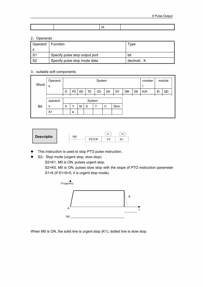
6 Pulse Output
nt
2、OperandsOperands
Function Type
S1 Specify pulse stop output port bitS2 Specify pulse stop mode data decimal,K
3、suitable soft components
This instruction is used to stop PTO pulse instruction. S2:Stop mode (urgent stop; slow stop).
S2=K1, M0 is ON, pulses urgent stop.S2=K0, M0 is ON, pulses slow stop with the slope of PTO instruction parameterS1+6 (If S1+6=0, it is urgent stop mode).
When M0 is ON, the solid line is urgent stop (K1), dotted line is slow stop.
operand
s
System
X Y M S T C Dn.m
S1 ●
Word
Descriptio
Bit
Operand
s
System constan
t
module
D FD ED TD CD DX DY DM DS K/H ID QD
S2 ●
PSTOP Y0 K1M0
S1· S2·
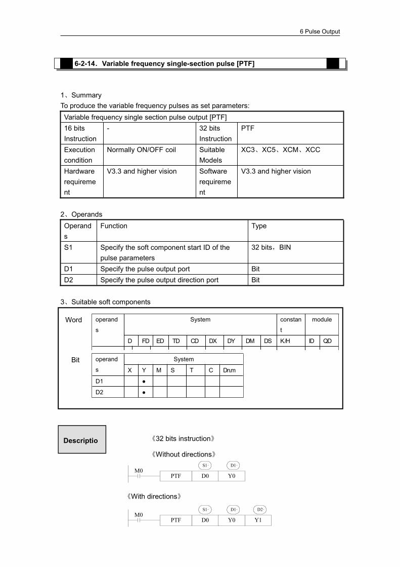
6 Pulse Output
6-2-14.Variable frequency single-section pulse [PTF]
1、SummaryTo produce the variable frequency pulses as set parameters:Variable frequency single section pulse output [PTF]16 bitsInstruction
- 32 bitsInstruction
PTF
Executioncondition
Normally ON/OFF coil SuitableModels
XC3、XC5、XCM、XCC
Hardwarerequirement
V3.3 and higher vision Softwarerequirement
V3.3 and higher vision
2、OperandsOperands
Function Type
S1 Specify the soft component start ID of thepulse parameters
32 bits,BIN
D1 Specify the pulse output port BitD2 Specify the pulse output direction port Bit
3、Suitable soft components
《32 bits instruction》
《Without directions》
《With directions》
operand
s
System
X Y M S T C Dn.m
D1 ●
D2 ●
Word
Descriptio
Bit
operand
s
System constan
t
module
D FD ED TD CD DX DY DM DS K/H ID QD
S1 ● ● ● ●
PTF D0 Y0M0
S1· D1·
PTF D0 Y0M0
S1· D1·
Y1
D2·
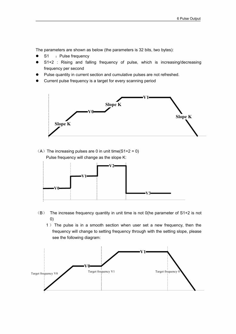
6 Pulse Output
The parameters are shown as below (the parameters is 32 bits, two bytes): S1 :Pulse frequency S1+2 : Rising and falling frequency of pulse, which is increasing/decreasing
frequency per second Pulse quantity in current section and cumulative pulses are not refreshed. Current pulse frequency is a target for every scanning period
(A)The increasing pulses are 0 in unit time(S1+2 = 0)Pulse frequency will change as the slope K:
(B) The increase frequency quantity in unit time is not 0(he parameter of S1+2 is not0)
1) The pulse is in a smooth section when user set a new frequency, then thefrequency will change to setting frequency through with the setting slope, pleasesee the following diagram:
V0
V1
V2
V3
Slope K
V0Slope K
V1
Slope K
Target frequency V0
V0
V1
Target frequency V1 Target frequency 0

6 Pulse Output
2)The pulse is in non-smooth section when user set a new frequency, then thefrequency will change to setting frequency with setting slope (current settingfrequency>last setting frequency, current setting frequency will be the target),please see the following diagram:
Before the frequency reaches V0, user set the new target frequency V1 (V1>V0),then the frequency will turn to V1 according to the slope.
3)The pulse is in non-smooth section, when user set the new frequency, thenchange to setting frequency with the setting slope (Current settingfrequency<last setting frequency, current setting frequency<current frequency),please see the following diagram:
Before the frequency reaches V0, user set the new target frequency V1 (V1<V0,V1<current frequency), it will go to the decreasing section until V1, the slope is thesame to the increasing section.
Target frequency V0
V2Target frequency V1 Target frequency 0
V0
V1
Target frequency V2
Target frequency V0
V2
Target frequency V1 Target frequency 0
V0
V1
Target frequency V2
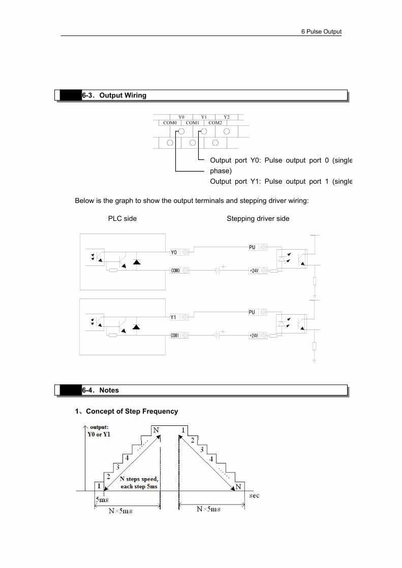
6 Pulse Output
6-3.Output Wiring
Y0COM0
Y1COM1
Y2COM2
Below is the graph to show the output terminals and stepping driver wiring:
Y0PU
PUY1
6-4.Notes
1、Concept of Step Frequency
PLC side Stepping driver side
Output port Y0: Pulse output port 0 (singlephase)Output port Y1: Pulse output port 1 (single

6 Pulse Output
频率的跳变
2、frequency jump in segment pulse output
When outputting the segmented pulse, if the current segment’s pulse has been setout, while meantime it doesn’t reach the highest frequency, then from the currentsegment to the next pulse output segment, pulse jump appears, see graph above;
To avoid frequency jump, please set suitable acceleration/deceleration time.
3、dual pulse output is invalid
D0PLSR D100 Y0M0
D200PLSR D1000 Y0M1
In the following cases, dual pulse output is invalid:(1)in main program
In one main program, users can’t write two or more pulse output instructions withone output port Y;
The below sample is wrong;
During ACC/DEC, each step time is 5ms, this time is fixed and not changeable. The minimum step frequency (each step’s rising/falling time) is 10Hz. If the
frequency is lower than 10Hz, calculate as 10Hz; the maximum step frequency is15Hz. If the frequency is larger than 15Hz, calculate as 15Hz;
In case of frequency larger than 200Hz, please make sure each segment’s pulsenumber no less than 10, if the set value is less than 10, send as 200Hz;
6 Pulse Output
(2)in STL
(3)in subprogram
(4)one in main program, another in STL
6 Pulse Output
(5)one in main program, another in subprogram
The correct programming method when it needs to write more than one pulse outputinstructions:Method 1: use STL, each STL only write one pulse output instructionExample:
6 Pulse Output
Note: the two STL cannot work at the same time! (M2 and M3 cannot be ON at the sametime)
Method2: if the same instruction needs to work in many places of the program, user canwrite one instruction in the main program, and put its parameter registers in STL.
6 Pulse Output
Method3: use sequence block. BLOCK can support multi-instruction sequential working.Please refer to chapter 10.
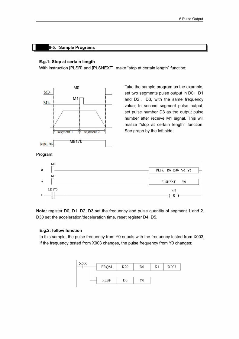
6 Pulse Output
6-5.Sample Programs
Program:
Note: register D0, D1, D2, D3 set the frequency and pulse quantity of segment 1 and 2.D30 set the acceleration/deceleration time, reset register D4, D5.
FRQM K20 D0 K1 X003X000
PLSF D0 Y0
E.g.2: follow functionIn this sample, the pulse frequency from Y0 equals with the frequency tested from X003.If the frequency tested from X003 changes, the pulse frequency from Y0 changes;
E.g.1: Stop at certain lengthWith instruction [PLSR] and [PLSNEXT], make “stop at certain length” function;
M0
M1
M8170
Take the sample program as the example,set two segments pulse output in D0、D1and D2, D3, with the same frequencyvalue; In second segment pulse output,set pulse number D3 as the output pulsenumber after receive M1 signal. This willrealize “stop at certain length” function.See graph by the left side;
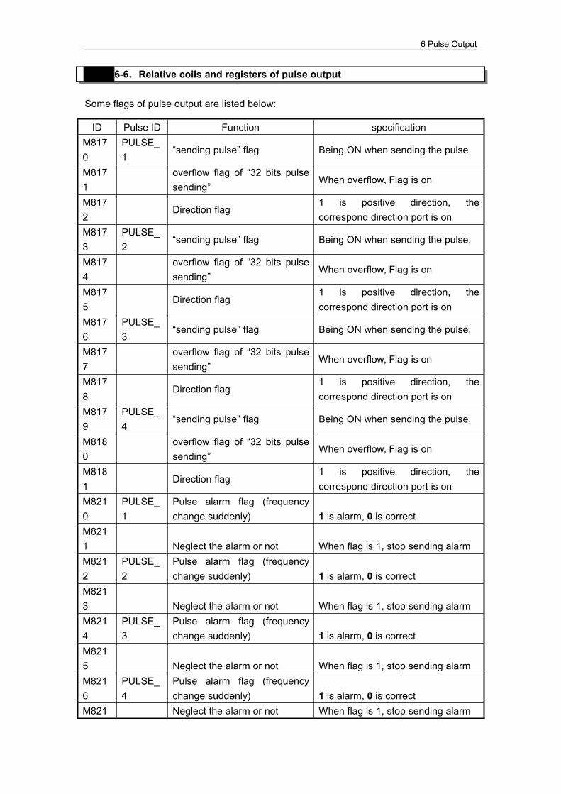
6 Pulse Output
6-6.Relative coils and registers of pulse output
Some flags of pulse output are listed below:
ID Pulse ID Function specificationM8170
PULSE_1
“sending pulse” flag Being ON when sending the pulse,
M8171
overflow flag of “32 bits pulsesending”
When overflow, Flag is on
M8172
Direction flag1 is positive direction, thecorrespond direction port is on
M8173
PULSE_2
“sending pulse” flag Being ON when sending the pulse,
M8174
overflow flag of “32 bits pulsesending”
When overflow, Flag is on
M8175
Direction flag1 is positive direction, thecorrespond direction port is on
M8176
PULSE_3
“sending pulse” flag Being ON when sending the pulse,
M8177
overflow flag of “32 bits pulsesending”
When overflow, Flag is on
M8178
Direction flag1 is positive direction, thecorrespond direction port is on
M8179
PULSE_4
“sending pulse” flag Being ON when sending the pulse,
M8180
overflow flag of “32 bits pulsesending”
When overflow, Flag is on
M8181
Direction flag1 is positive direction, thecorrespond direction port is on
M8210
PULSE_1
Pulse alarm flag (frequencychange suddenly) 1 is alarm, 0 is correct
M8211 Neglect the alarm or not When flag is 1, stop sending alarmM8212
PULSE_2
Pulse alarm flag (frequencychange suddenly) 1 is alarm, 0 is correct
M8213 Neglect the alarm or not When flag is 1, stop sending alarmM8214
PULSE_3
Pulse alarm flag (frequencychange suddenly) 1 is alarm, 0 is correct
M8215 Neglect the alarm or not When flag is 1, stop sending alarmM8216
PULSE_4
Pulse alarm flag (frequencychange suddenly) 1 is alarm, 0 is correct
M821 Neglect the alarm or not When flag is 1, stop sending alarm

6 Pulse Output
Some special registers of pulse output are listed below:
7M8218
PULSE_5
Pulse alarm flag (frequencychange suddenly) 1 is alarm, 0 is correct
M8219 Neglect the alarm or not When flag is 1, stop sending alarm
ID Pulse ID Function Specification
D8170 PULSE_1The low 16 bits of accumulated pulsenumber
D8171The high 16 bits of accumulated pulsenumber
D8172 The current segment (means segment n)
D8173 PULSE_2The low 16 bits of accumulated pulsenumber
D8174The high 16 bits of accumulated pulsenumber
D8175The current segment ( means segmentn )
D8176 PULSE_3The low 16 bits of accumulated pulsenumber
D8177The high 16 bits of accumulated pulsenumber
D8178The current segment ( means segmentn )
D8179 PULSE_4The low 16 bits of accumulated pulsenumber
D8180The high 16 bits of accumulated pulsenumber
D8181The current segment ( means segmentn )
D8190 PULSE_1The low 16 bits of the currentaccumulated current pulse number
D8191The high 16 bits of the currentaccumulated current pulse number
D8192 PULSE_2The low 16 bits of the currentaccumulated current pulse number
D8193 The high 16 bits of the current

6 Pulse Output
Absolute position/relative position/back to origin;
Note: for frequency rising time of absolution/relative positioning instruction, the registersetting value should meet the following formula:
Register (D8230, D8232……)Rising time(ms) × max
100K
accumulated current pulse number
D8194 PULSE_3The low 16 bits of the currentaccumulated current pulse number
Only XC5-32RT-E(4PLS) model has
D8195The high 16 bits of the currentaccumulated current pulse number
D8196 PULSE_4The low 16 bits of the currentaccumulated current pulse number
D8197The high 16 bits of the currentaccumulated current pulse number
D8210 PULSE_1 The error pulse segment’s positionD8212 PULSE_2 The error pulse segment’s positionD8214 PULSE_3 The error pulse segment’s positionD8216 PULSE_4 The error pulse segment’s positionD8218 PULSE_5 The error pulse segment’s position
ID Pulse Function Description
D8230PULSE_1
Rising time of the absolute/relation positioninstruction (Y0)
D8231Falling time of the origin return instruction(Y0)
D8232PULSE_2
Rising time of the absolute/relation positioninstruction (Y1)
D8233Falling time of the origin return instruction(Y1)
D8234PULSE_3
Rising time of the absolute/relation positioninstruction (Y2)
D8235Falling time of the origin return instruction(Y2)
D8236PULSE_4
Rising time of the absolute/relation positioninstruction (Y3)
D8237Falling time of the origin return instruction(Y3)
D8238PULSE_5
Rising time of the absolute/relation positioninstruction
D8239 Falling time of the origin return instruction

6 Pulse Output
For example: instruction DRVA K300080 K3000 Y0 Y4, rising time is 100ms.Then register D8230 (Dword) = 3=[100(ms)×3000(Hz)] ÷100K(Hz).
7 Communication Function
7 Communication Function
This chapter mainly includes: basic concept of communication, Modbus communication,free communication and CAN-bus communication;
7-1.Summary
7-2.Modbus Communication
7-3.Free Communication
7-4.CAN Communication
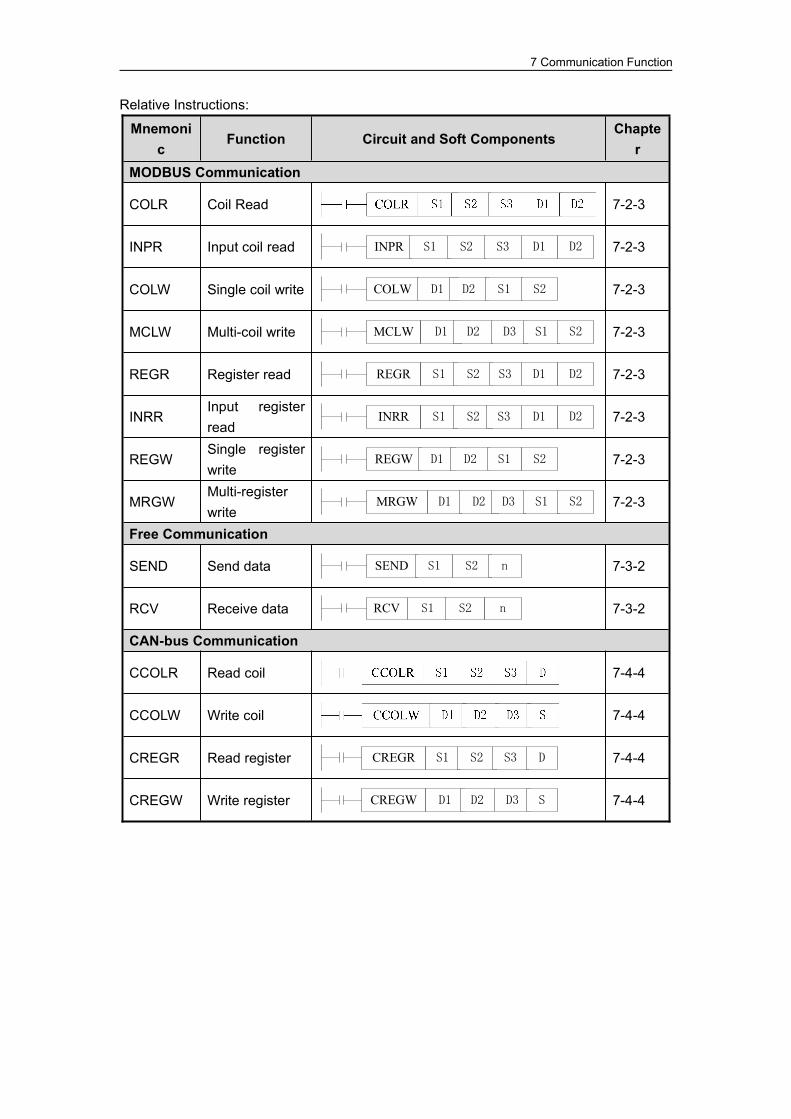
7 Communication Function
Relative Instructions:
Mnemonic
Function Circuit and Soft ComponentsChapte
rMODBUS Communication
COLR Coil Read 7-2-3
INPR Input coil read INPR S1 S2 S3 D1 D2 7-2-3
COLW Single coil write COLW D1 D2 S1 S2 7-2-3
MCLW Multi-coil write MCLW D1 D2 D3 S1 S2 7-2-3
REGR Register read REGR S1 S2 S3 D1 D2 7-2-3
INRRInput registerread
INRR S1 S2 S3 D1 D2 7-2-3
REGWSingle registerwrite
REGW D1 D2 S1 S2 7-2-3
MRGWMulti-registerwrite
MRGW D1 D2 D3 S1 S2 7-2-3
Free Communication
SEND Send data SEND S1 S2 n 7-3-2
RCV Receive data RCV S1 S2 n 7-3-2
CAN-bus Communication
CCOLR Read coil 7-4-4
CCOLW Write coil 7-4-4
CREGR Read register CREGR S1 S2 S3 D 7-4-4
CREGW Write register CREGW D1 D2 D3 S 7-4-4
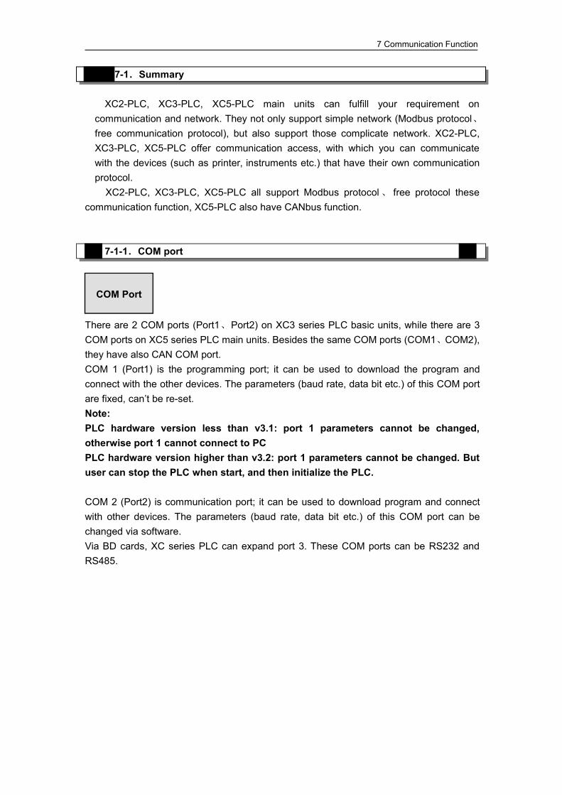
7 Communication Function
7-1.Summary
XC2-PLC, XC3-PLC, XC5-PLC main units can fulfill your requirement oncommunication and network. They not only support simple network (Modbus protocol、free communication protocol), but also support those complicate network. XC2-PLC,XC3-PLC, XC5-PLC offer communication access, with which you can communicatewith the devices (such as printer, instruments etc.) that have their own communicationprotocol.XC2-PLC, XC3-PLC, XC5-PLC all support Modbus protocol、 free protocol these
communication function, XC5-PLC also have CANbus function.
7-1-1.COM port
There are 2 COM ports (Port1、Port2) on XC3 series PLC basic units, while there are 3COM ports on XC5 series PLC main units. Besides the same COM ports (COM1、COM2),they have also CAN COM port.COM 1 (Port1) is the programming port; it can be used to download the program andconnect with the other devices. The parameters (baud rate, data bit etc.) of this COM portare fixed, can’t be re-set.Note:PLC hardware version less than v3.1: port 1 parameters cannot be changed,otherwise port 1 cannot connect to PCPLC hardware version higher than v3.2: port 1 parameters cannot be changed. Butuser can stop the PLC when start, and then initialize the PLC.
COM 2 (Port2) is communication port; it can be used to download program and connectwith other devices. The parameters (baud rate, data bit etc.) of this COM port can bechanged via software.Via BD cards, XC series PLC can expand port 3. These COM ports can be RS232 andRS485.
COM Port
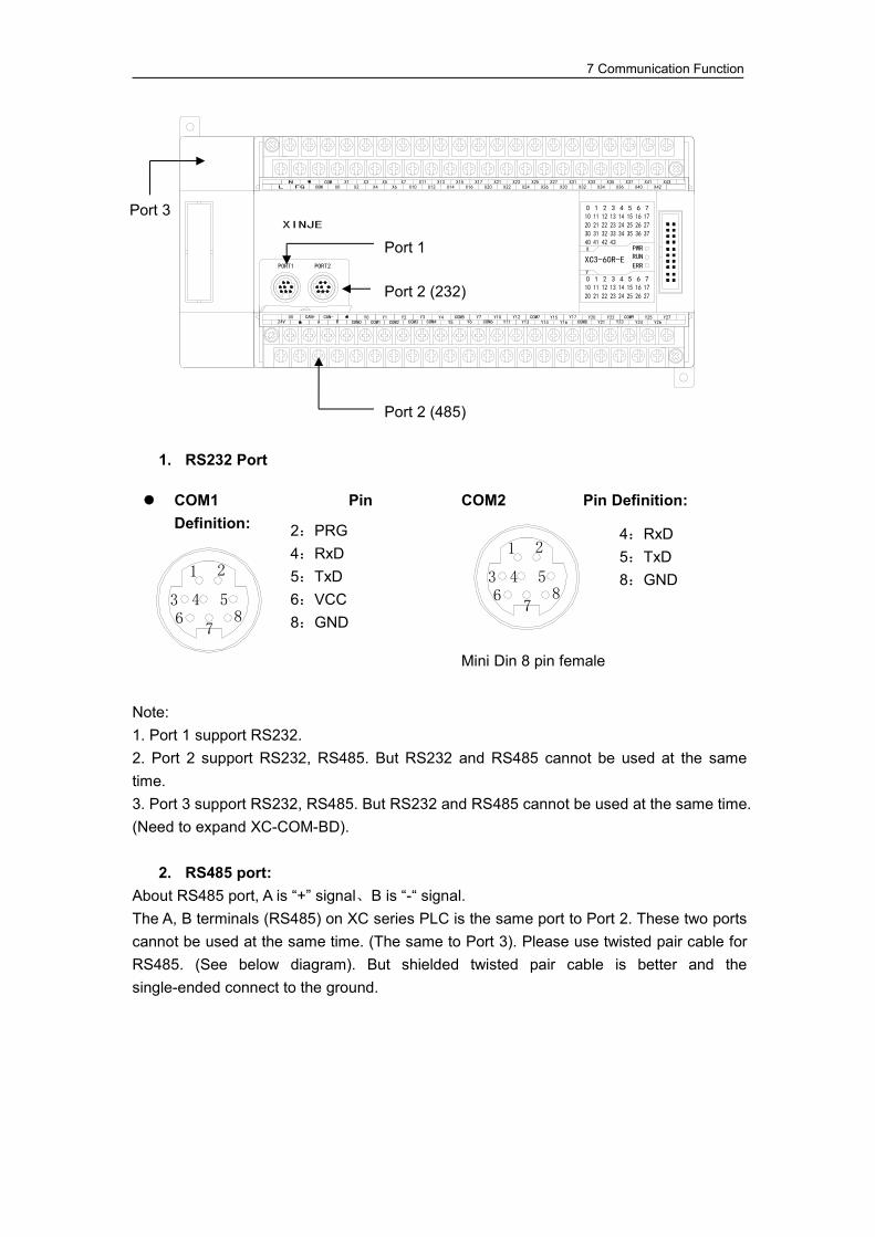
7 Communication Function
COM9COM8
Y
X
X0X1COM
COM X2X3X4X5X6X7X10X11X12X13X14X15X16X17X20X21X22X23X24X25X26X27X30
X37X40X36
X35X34
X33X32
X31 X41X42X43
Y27Y26
Y25Y24
Y15 Y17COM6 Y21
Y20COM7Y23
Y22Y16Y13 Y14
COM5Y11Y12Y7 Y10
Y6COM4Y4Y5COM3
Y3Y2Y1COM2
Y0COM1COM0
CAN+ CAN-A B
0V24V
PORT2PORT1XC3-60R-E
ERR
RUNPWR
0 1 32 6 754
4 5 762 310
1. RS232 Port
Note:1. Port 1 support RS232.2. Port 2 support RS232, RS485. But RS232 and RS485 cannot be used at the sametime.3. Port 3 support RS232, RS485. But RS232 and RS485 cannot be used at the same time.(Need to expand XC-COM-BD).
2. RS485 port:About RS485 port, A is “+” signal、B is “-“ signal.The A, B terminals (RS485) on XC series PLC is the same port to Port 2. These two portscannot be used at the same time. (The same to Port 3). Please use twisted pair cable forRS485. (See below diagram). But shielded twisted pair cable is better and thesingle-ended connect to the ground.
COM1 PinDefinition:
3 4 5
1 2
6 87
2:PRG4:RxD5:TxD6:VCC8:GND
COM2 Pin Definition:
3 4 5
1 2
6 87
Mini Din 8 pin female
4:RxD5:TxD8:GND
Port 1
Port 2 (232)
Port 3
Port 2 (485)

7 Communication Function
3. CAN port:CAN port can be applied to CANBUS communication. The pin terminals are “CAN+”,“CAN-“For the detailed CAN communication functions, please refer to chapter 7-4 CAN busfunction.
Send Receive
Receive Send
Interference

7-1-2.Communication Parameters
Station Modbus Station number: 1~254、255 (FF) is free format communicationBaud Rate 300bps~115.2KbpsData Bit 8 bits data、7 bits dataStop Bit 2 stop bits、1 stop bitParity Even、Odd、No check
The default parameters of COM 1:Station number is 1、baud rate is 19200bps、8 data bit、1 stop bit、Even parity
COM 1
Number Function Description
FD8210 Communication mode255 is free format,1~254 bit is Modbus stationnumber
FD8211 Communication format Baud rate, data bit, stop bit, parity
FD8212 ASC timeout judgment timeUnit: ms, if set to be 0, it means notimeout waiting
FD8213Reply timeout judgmenttime
Unit: ms, if set to be 0, it means notimeout waiting
FD8214 Start symbol High 8 bits invalidFD8215 End symbol High 8 bits invalid
FD8216 Free format setting8/16 bits cushion,with/without start bit,with/without stop bit
COM 2
FD8220 Communication mode255 is free format,1~254 bit is Modbus stationnumber
FD8221 Communication format Baud rate, data bit, stop bit, parity
FD8222 ASC timeout judgment timeUnit: ms, if set to be 0, it means notimeout waiting
FD8223Reply timeout judgmenttime
Unit: ms, if set to be 0, it means notimeout waiting
FD8224 Start symbol High 8 bits invalid
Parameters Setting
Set the parameters with the COM ports on XC series PLC;
Communication
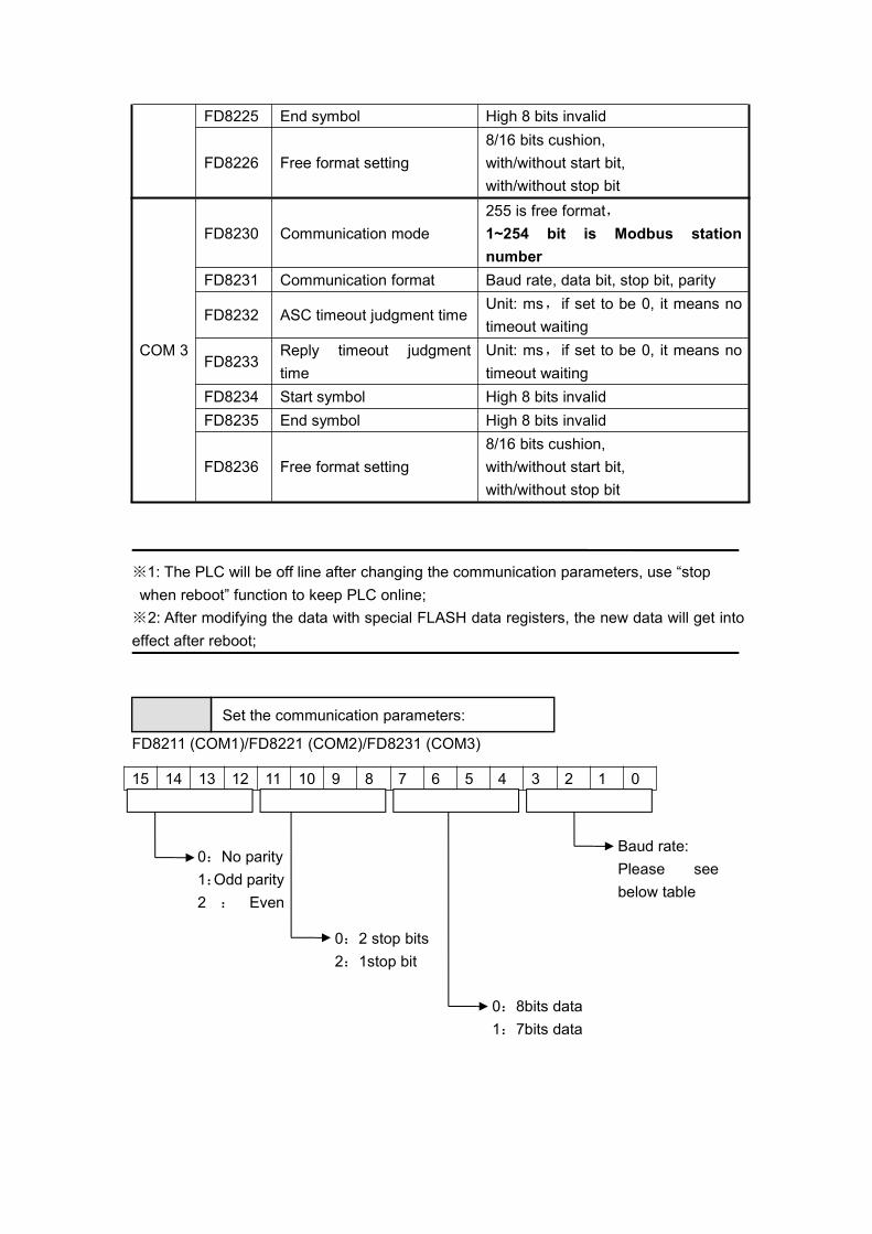
Baud rate:Please seebelow table
0:8bits data1:7bits data
0:2 stop bits2:1stop bit
0:No parity1:Odd parity2 : Even
FD8225 End symbol High 8 bits invalid
FD8226 Free format setting8/16 bits cushion,with/without start bit,with/without stop bit
COM 3
FD8230 Communication mode255 is free format,1~254 bit is Modbus stationnumber
FD8231 Communication format Baud rate, data bit, stop bit, parity
FD8232 ASC timeout judgment timeUnit: ms, if set to be 0, it means notimeout waiting
FD8233Reply timeout judgmenttime
Unit: ms, if set to be 0, it means notimeout waiting
FD8234 Start symbol High 8 bits invalidFD8235 End symbol High 8 bits invalid
FD8236 Free format setting8/16 bits cushion,with/without start bit,with/without stop bit
※1: The PLC will be off line after changing the communication parameters, use “stopwhen reboot” function to keep PLC online;
※2: After modifying the data with special FLASH data registers, the new data will get intoeffect after reboot;
FD8211 (COM1)/FD8221 (COM2)/FD8231 (COM3)
15 14 13 12 11 10 9 8 7 6 5 4 3 2 1 0
Set the communication parameters:

0: 8 bitscommunication
0: without start symbol1: with start symbol
0: without end symbol1: with end symbol
Reserve
bit0~bit3 baud rate:Baud rate Suitable
typeBaud rate Suitable type
0:300bps XC1 0:768Kbps - XC2、XCM、XCC1:600bps XC1 1:600bps XC3、XC5 XC2、XCM、XCC2:1200 bps XC1 2:1200 bps XC3、XC5 XC2、XCM、XCC3:2400 bps XC1 3:2400 bps XC3、XC5 XC2、XCM、XCC4:4800 bps XC1 4:4800 bps XC3、XC5 XC2、XCM、XCC5:9600 bps XC1 5:9600 bps XC3、XC5 XC2、XCM、XCC6:19.2K bps XC1 6:19.2Kbps XC3、XC5 XC2、XCM、XCC7:38.4K bps XC1 7:38.4Kbps XC3、XC5 XC2、XCM、XCC8:57.6K bps XC1 8:57.6Kbps XC3、XC5 -9:115.2K bps XC1 9:115.2Kbps XC3、XC5 -- - A:192Kbps XC3、XC5 XC2、XCM、XCC- - B:256Kbps - XC2、XCM、XCC- - C:288Kbps XC3、XC5 -- - D:384Kbps XC3、XC5 XC2、XCM、XCC- - E:512Kbps - XC2、XCM、XCC- - F:576Kbps XC3、XC5 -
FD8216 (COM1)/FD8226 (COM2)/FD8236 (COM3)
Note: user doesn’t have to calculate the FD value to set the communication parameter.Please set the parameters in XCPpro software.
15 14 13 12 11 10 9 8 7 6 5 4 3 2 1 0

After changing the parameters, please restart the PLC to make it effective.

7-2.MODBUS Communication
7-2-1.Function
XC series PLC support both Modbus master and Modbus slave.Master mode: When PLC is set to be master, PLC sends request to other slave devices
via Modbus instructions, other devices response the master. For example,Spectra PLC can control the inverter through Modbus.
Slave mode: when PLC is set to be slave, it can only response with other master devices.
Master and slave: in RS485 network, there are one maser and several slaves at one time(see below diagram). The master station can read and write any slave stations.Two slave stations cannot communicate with each other. Master stationcommunicates with slave station through Modbus instructions. Slave stationhas no program but only response the master station. (wiring: connect all theRS485 +, connect all the RS485-)
Master
Slave1
Slave2
Slave3
In RS232 network, there is only one master and one slave.
SlaveMaste
There is dotted line in the diagram. It means any PLC can be master station when theentire PLC in the network don’t send data. But more than one PLC will send data at onetime, the communication will fail. It is not recommended to use.
Note: For XC series PLC, RS232 only support half-duplex.
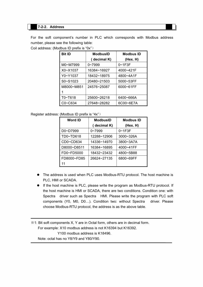
7-2-2.Address
For the soft component’s number in PLC which corresponds with Modbus addressnumber, please see the following table:Coil address: (Modbus ID prefix is “0x”)
Bit ID ModbusID( decimal K)
Modbus ID(Hex. H)
M0~M7999 0~7999 0~1F3FX0~X1037 16384~16927 4000~421FY0~Y1037 18432~18975 4800~4A1FS0~S1023 20480~21503 5000~53FFM8000~M8511
24576~25087 6000~61FF
T0~T618 25600~26218 6400~666AC0~C634 27648~28282 6C00~6E7A
Register address: (Modbus ID prefix is “4x”)Word ID ModbusID
( decimal K)Modbus ID(Hex. H)
D0~D7999 0~7999 0~1F3FTD0~TD618 12288~12906 3000~326ACD0~CD634 14336~14970 3800~3A7AD8000~D8511 16384~16895 4000~41FFFD0~FD5000 18432~23432 4800~5B88FD8000~FD8511
26624~27135 6800~69FF
The address is used when PLC uses Modbus-RTU protocol. The host machine isPLC, HMI or SCADA.
If the host machine is PLC, please write the program as Modbus-RTU protocol. Ifthe host machine is HMI or SCADA, there are two conditions. Condition one: withSpectra driver such as Spectra HMI. Please write the program with PLC softcomponents (Y0, M0, D0…). Condition two: without Spectra driver. Pleasechoose Modbus-RTU protocol, the address is as the above table.
※1: Bit soft components X, Y are in Octal form, others are in decimal form.For example: X10 modbus address is not K16394 but K16392.
Y100 modbus address is K18496.Note: octal has no Y8/Y9 and Y80/Y90.
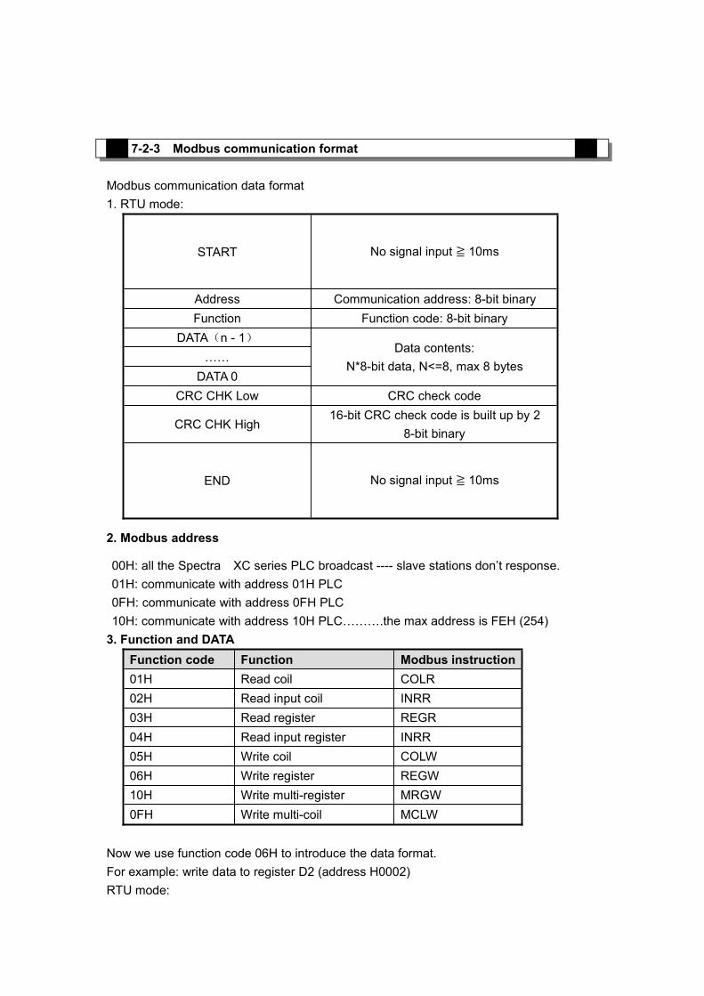
7-2-3 Modbus communication format
Modbus communication data format1. RTU mode:
START No signal input ≧ 10ms
Address Communication address: 8-bit binaryFunction Function code: 8-bit binary
DATA(n - 1)Data contents:
N*8-bit data, N<=8, max 8 bytes……
DATA 0CRC CHK Low CRC check code
CRC CHK High16-bit CRC check code is built up by 2
8-bit binary
END No signal input ≧ 10ms
2. Modbus address
00H: all the Spectra XC series PLC broadcast ---- slave stations don’t response.01H: communicate with address 01H PLC0FH: communicate with address 0FH PLC10H: communicate with address 10H PLC……….the max address is FEH (254)3. Function and DATA
Function code Function Modbus instruction01H Read coil COLR02H Read input coil INRR03H Read register REGR04H Read input register INRR05H Write coil COLW06H Write register REGW10H Write multi-register MRGW0FH Write multi-coil MCLW
Now we use function code 06H to introduce the data format.For example: write data to register D2 (address H0002)RTU mode:
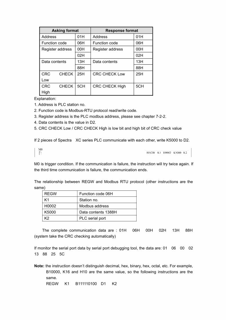
Asking format Response formatAddress 01H Address 01HFunction code 06H Function code 06HRegister address 00H Register address 00H
02H 02HData contents 13H Data contents 13H
88H 88HCRC CHECKLow
25H CRC CHECK Low 25H
CRC CHECKHigh
5CH CRC CHECK High 5CH
Explanation:1. Address is PLC station no.2. Function code is Modbus-RTU protocol read/write code.3. Register address is the PLC modbus address, please see chapter 7-2-2.4. Data contents is the value in D2.5. CRC CHECK Low / CRC CHECK High is low bit and high bit of CRC check value
If 2 pieces of Spectra XC series PLC communicate with each other, write K5000 to D2.
M0 is trigger condition. If the communication is failure, the instruction will try twice again. Ifthe third time communication is failure, the communication ends.
The relationship between REGW and Modbus RTU protocol (other instructions are thesame)
REGW Function code 06HK1 Station no.H0002 Modbus addressK5000 Data contents 1388HK2 PLC serial port
The complete communication data are : 01H 06H 00H 02H 13H 88H(system take the CRC checking automatically)
If monitor the serial port data by serial port debugging tool, the data are: 01 06 00 0213 88 25 5C
Note: the instruction doesn’t distinguish decimal, hex, binary, hex, octal, etc. For example,B10000, K16 and H10 are the same value, so the following instructions are thesame.REGW K1 B111110100 D1 K2

REGW K1 K500 D1 K2REGW K1 H1F4 D1 K2
7-2-4.Communication Instructions
Modbus instructions include coil read/write, register read/write; below, we describe theseinstructions in details:
The operand definition in the instruction:
1. Remote communication station and serial port number
For example, one PLC connects 3 inverters. PLC needs to write and read the parametersof inverter. The inverter station no. is 1, 2, and 3. So the remote communication station no.is 1, 2, and 3.
2. Remote register/coil quantity
For example, PLC read inverter frequency (H2103), output current (H2104) and busvoltage (H2105). So the remote register first address is H2103, quantity is K3 (3registers).
3. Local coil/register address
For example, local coil is M0, write the M0 state to remote coil.
Local register is D0, write the D0 value to remote register.
Coil Read [COLR]
1、Instruction SummaryRead the specified station’s specified coil status to the local PLC;Coil read [COLR]16 bitsinstruction
COLR 32 bitsinstruction
-
ExecutionCondition
Normally ON/OFF coil SuitableModels
XC2, XC3, XC5, XCM, XCC

HardwareRequirement
- SoftwareRequirement
-
2、OperandsOperands
Function Type
S1 Specify the remote communication station 16bits, BINS2 Specify the remote coil first address 16bits, BINS3 Specify the coil quantity 16bits, BIND1 Specify the local coil first address bitD2 Specify the serial port no. 16bits, BIN
3、suitable soft components
COLR K1 K500 K3 M1X0
K2
S1· S2· S3· D1· D2·
Read coil instruction, Modbus function code is 01H Serial Port: K1~K3 Operand S3: K1~K984, the max coil quantity is 984
Input Coil Read [INPR]
1、InstructionRead the specified station’s specified input coils into local coils:Input coil read [INPR]16 bitsinstruction
INPR 32 bitsinstruction
-
Operan
ds
Operands
X Y M S T C Dn.m
D1 ● ● ● ● ● ●
Word
Function
Bit
Operan
ds
System consta
nt
module
D FD ED TD CD DX DY DM DS K/H ID QD
S1 ● ● ● ● ●
S2 ● ● ● ● ●
S3 ● ● ● ● ●
D2 K
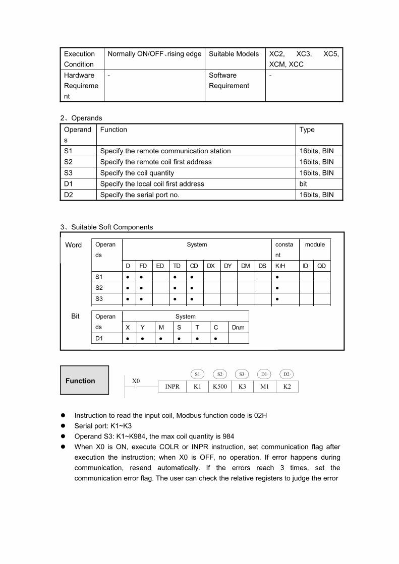
ExecutionCondition
Normally ON/OFF、rising edge Suitable Models XC2, XC3, XC5,XCM, XCC
HardwareRequirement
- SoftwareRequirement
-
2、OperandsOperands
Function Type
S1 Specify the remote communication station 16bits, BINS2 Specify the remote coil first address 16bits, BINS3 Specify the coil quantity 16bits, BIND1 Specify the local coil first address bitD2 Specify the serial port no. 16bits, BIN
3、Suitable Soft Components
INPR K1 K500 K3 M1X0
K2
S1· S2· S3· D1· D2·
Instruction to read the input coil, Modbus function code is 02H Serial port: K1~K3 Operand S3: K1~K984, the max coil quantity is 984 When X0 is ON, execute COLR or INPR instruction, set communication flag after
execution the instruction; when X0 is OFF, no operation. If error happens duringcommunication, resend automatically. If the errors reach 3 times, set thecommunication error flag. The user can check the relative registers to judge the error
Operan
ds
System
X Y M S T C Dn.m
D1 ● ● ● ● ● ●
Word
Function
Bit
Operan
ds
System consta
nt
module
D FD ED TD CD DX DY DM DS K/H ID QD
S1 ● ● ● ● ●
S2 ● ● ● ● ●
S3 ● ● ● ● ●
D2 K

single coil write [COLW]
1、summaryWrite the local coil status to the specified station’s specified coil;Single coil write [COLW]16 bitsinstruction
COLW 32 bitsinstruction
-
ExecutionCondition
Normally ON/OFF、rising edge SuitableModels
XC2, XC3, XC5, XCM,XCC
HardwareRequirement
- SoftwareRequirement
-
2、OperandsOperands
Function Type
D1 Specify the remote communication station 16bits, BIND2 Specify the remote coil first address 16bits, BINS1 Specify the local coil first address bitS2 Specify the serial port no. 16bits, BIN
3、suitable soft components
COLW K1 K500 M1X0
K2
D1· D2· S1· S2·
Write the single coil, Modbus function code is 05H
Operan
ds
System
X Y M S T C Dn.m
S1 ● ● ● ● ● ●
Word
Function
Bit
Operan
ds
System consta
nt
module
D FD ED TD CD DX DY DM DS K/H ID QD
D1 ● ● ● ● ●
D2 ● ● ● ● ●
S2 K
Serial port: K1~K3
multi-coil write [MCLW]
1、SummaryWrite the local multi-coil status into the specified station’s specified coil;Multi-coil write [MCLW]16 bitsinstruction
MCLW 32 bitsinstruction
-
ExecutionCondition
Normally ON/OFF、rising edge Suitable Models XC2, XC3, XC5,XCM, XCC
HardwareRequirement
- SoftwareRequirement
-
2、OperandsOperands
Function Type
D1 Specify the remote communication station 16bits, BIND2 Specify the remote coil first address 16bits, BIND3 Specify the coil quantity 16bits, BINS1 Specify the local coil first address bitS2 Specify the serial port no. 16bits, BIN
3、Suitable soft components
Operan
ds
System
X Y M S T C Dn.m
S1 ● ● ● ● ● ●
Word
Bit
Operan
ds
System consta
nt
module
D FD ED TD CD DX DY DM DS K/H ID QD
D1 ● ● ● ● ●
D2 ● ● ● ● ●
D3 ● ● ● ● ●
S2 K
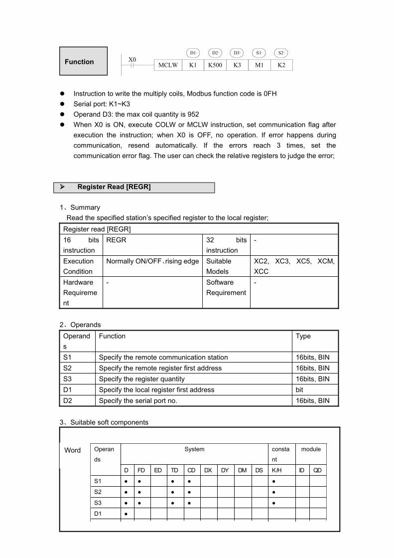
MCLW K1 K500 K3 M1X0
K2
D1· S1· S2·D2· D3·
Instruction to write the multiply coils, Modbus function code is 0FH Serial port: K1~K3 Operand D3: the max coil quantity is 952 When X0 is ON, execute COLW or MCLW instruction, set communication flag after
execution the instruction; when X0 is OFF, no operation. If error happens duringcommunication, resend automatically. If the errors reach 3 times, set thecommunication error flag. The user can check the relative registers to judge the error;
Register Read [REGR]
1、SummaryRead the specified station’s specified register to the local register;Register read [REGR]16 bitsinstruction
REGR 32 bitsinstruction
-
ExecutionCondition
Normally ON/OFF、rising edge SuitableModels
XC2, XC3, XC5, XCM,XCC
HardwareRequirement
- SoftwareRequirement
-
2、OperandsOperands
Function Type
S1 Specify the remote communication station 16bits, BINS2 Specify the remote register first address 16bits, BINS3 Specify the register quantity 16bits, BIND1 Specify the local register first address bitD2 Specify the serial port no. 16bits, BIN
3、Suitable soft components
Function
Word Operan
ds
System consta
nt
module
D FD ED TD CD DX DY DM DS K/H ID QD
S1 ● ● ● ● ●
S2 ● ● ● ● ●
S3 ● ● ● ● ●
D1 ●
D2 K
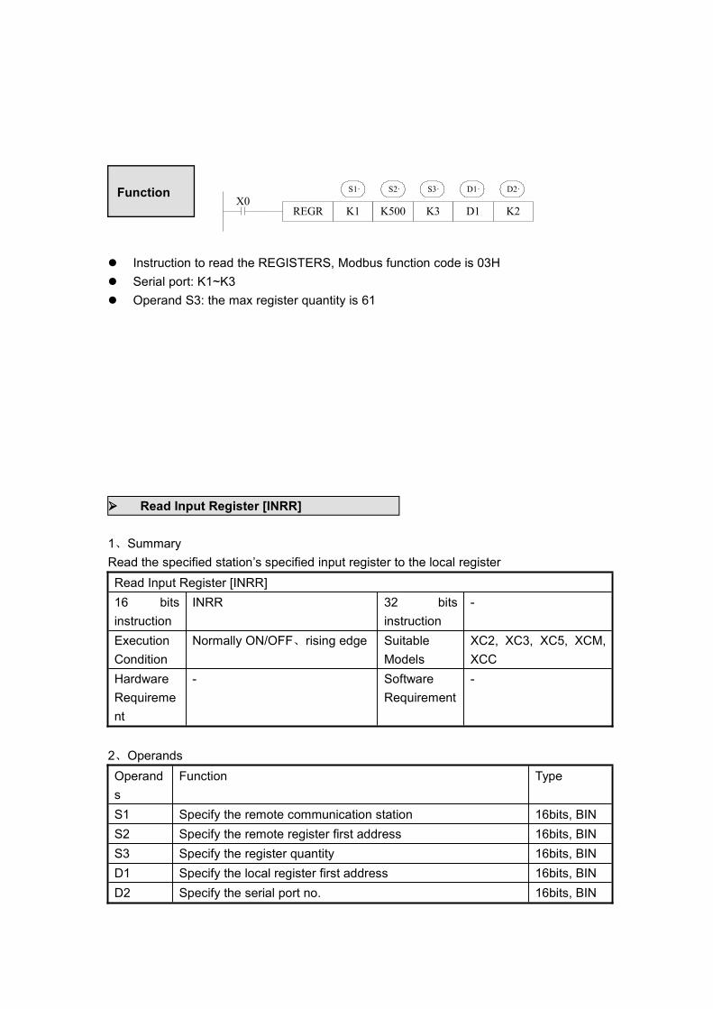
REGR K1 K500 K3 D1X0
K2
S1· S2· S3· D1· D2·
Instruction to read the REGISTERS, Modbus function code is 03H Serial port: K1~K3 Operand S3: the max register quantity is 61
Read Input Register [INRR]
1、SummaryRead the specified station’s specified input register to the local registerRead Input Register [INRR]16 bitsinstruction
INRR 32 bitsinstruction
-
ExecutionCondition
Normally ON/OFF、rising edge SuitableModels
XC2, XC3, XC5, XCM,XCC
HardwareRequirement
- SoftwareRequirement
-
2、OperandsOperands
Function Type
S1 Specify the remote communication station 16bits, BINS2 Specify the remote register first address 16bits, BINS3 Specify the register quantity 16bits, BIND1 Specify the local register first address 16bits, BIND2 Specify the serial port no. 16bits, BIN
Function

3、Suitable soft components
INRR K1 K500 K3 D1X0
K2
S1· S2· S3· D1· D2·
Instruction to read the input registers, Modbus function code is 04H Serial port: K1~K3 Operand S3: the max input register quantity is 61 When X0 is ON, execute REGR or INRR instruction, set communication flag after
execution the instruction; when X0 is OFF, no operation. If error happens duringcommunication, resend automatically. If the errors reach 4 times, set thecommunication error flag. The user can check the relative registers to judge the error;
Single register write [REGW]
1、summaryInstruction to write the local specified register into the specified station’s specified
register;Single register write [REGW]16 bitsinstruction
REGW 32 bitsinstruction
-
ExecutionCondition
Normally ON/OFF、rising edge SuitableModels
XC2, XC3, XC5, XCM,XCC
HardwareRequirement
- SoftwareRequirement
-
2、OperandsOperands
Function Type
D1 Specify the remote communication station 16bits, BIND2 Specify the remote register first address 16bits, BIN
Word
Function
Operan
ds
System consta
nt
module
D FD ED TD CD DX DY DM DS K/H ID QD
S1 ● ● ● ● ●
S2 ● ● ● ● ●
S3 ● ● ● ● ●
D1 ●
D2 K

S1 Specify the local register first address 16bits, BINS2 Specify the serial port no. 16bits, BIN
3、Suitable soft components
REGW K1 K500 D1X0
K2
D1· S1· S2·D2·
Write the single register, Modbus function code is 06H Serial port: K1~K3
Multi-register write [MRGW]
1、SummaryInstruction to write the local specified register to the specified station’s specified
register;Multi-register write [MRGW]16 bitsinstruction
MRGW 32 bitsinstruction
-
ExecutionCondition
Normally ON/OFF 、 risingedge
SuitableModels
XC2, XC3, XC5, XCM, XCC
HardwareRequirement
- SoftwareRequirement
-
2、OperandsOperan Function Type
Word
Function
Operan
ds
System consta
nt
module
D FD ED TD CD DX DY DM DS K/H ID QD
D1 ● ● ● ● ●
D2 ● ● ● ● ●
S1 ●
S2 K
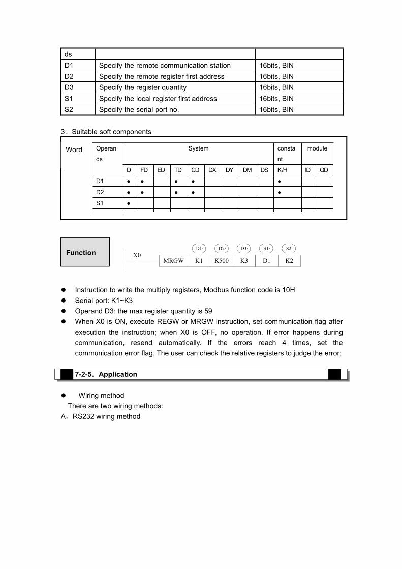
dsD1 Specify the remote communication station 16bits, BIND2 Specify the remote register first address 16bits, BIND3 Specify the register quantity 16bits, BINS1 Specify the local register first address 16bits, BINS2 Specify the serial port no. 16bits, BIN
3、Suitable soft components
MRGW K1 K500 K3 D1X0
K2
D1· D2· D3· S1· S2·
Instruction to write the multiply registers, Modbus function code is 10H Serial port: K1~K3 Operand D3: the max register quantity is 59 When X0 is ON, execute REGW or MRGW instruction, set communication flag after
execution the instruction; when X0 is OFF, no operation. If error happens duringcommunication, resend automatically. If the errors reach 4 times, set thecommunication error flag. The user can check the relative registers to judge the error;
7-2-5.Application
Wiring methodThere are two wiring methods:
A、RS232 wiring method
Word Operan
ds
System consta
nt
module
D FD ED TD CD DX DY DM DS K/H ID QD
D1 ● ● ● ● ●
D2 ● ● ● ● ●
S1 ●
S2 K
Function
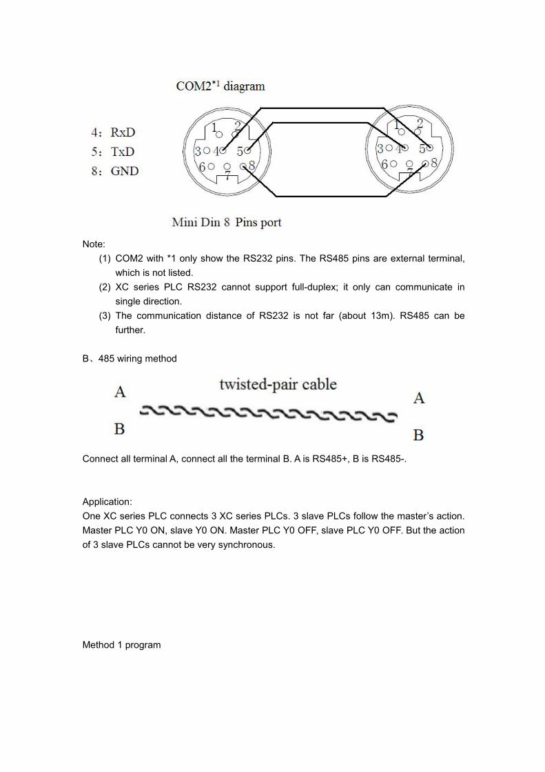
Note:(1) COM2 with *1 only show the RS232 pins. The RS485 pins are external terminal,
which is not listed.(2) XC series PLC RS232 cannot support full-duplex; it only can communicate in
single direction.(3) The communication distance of RS232 is not far (about 13m). RS485 can be
further.
B、485 wiring method
Connect all terminal A, connect all the terminal B. A is RS485+, B is RS485-.
Application:One XC series PLC connects 3 XC series PLCs. 3 slave PLCs follow the master’s action.Master PLC Y0 ON, slave Y0 ON. Master PLC Y0 OFF, slave PLC Y0 OFF. But the actionof 3 slave PLCs cannot be very synchronous.
Method 1 program

There are 3 STL in the program. Every STL is communication program of one slave. If oneSTL communication is successful, it jumps to the next STL. If not, it tries twice. If threetimes all fail, M8137 is ON and jump to the next STL. (This program uses serial port 2, ifit is other serial port, please see appendix 1 for communication flag bit)
Method 2: use BLOCK to make the program

M8000 is always ON coil, the master will keep on writing the Y0 state to slave Y0. (Pleaserefer to chapter 10 for BLOCK function).
Method 3: use broadcast function
When master Y0 state changes, it broadcasts the state to all the slaves. Thesynchronization is better than method 1 and 2.

7-3.FREE FORMAT COMMUNICATION
7-3-1.Communication mode
Free format communication transfer data in the form of data block, each block can transfer128 bytes at most.Free format communication modeFree format is free protocol communication. Now many devices support RS232 or RS485,but the communication protocol is different. For example, Spectra PLC is Modbusprotocol, some temperature controllers use special protocol. If PLC needs to readtemperature, it can send data according to the temperature controller protocol.
Note: Port1, Port2 or Port3 can support free format communication, but free format usually
needs to change the serial port parameters. Port 1 parameter cannot be changed, soit is not recommended to use port 1.
In free format mode, FD8220 (port 2) or FD8230 (port 3) should set to be 255 (FF) Baud Rate: 300bps~115.2Kbps Data Format
Data Bit: 7bits, 8bitsParity: Odd, Even, No CheckStop bit: 1 bit, 2 bits
Start bit: 1 bitStop bit: 1 bitUser can set a start/stop bit, then PLC will automatically add this start/stop bit whensending data; remove this start/stop bit when receiving data.Start bit and stop bit can be seemed as header and frame end. If slave station hasstarted and stop bit, they can be set in software or protocol.
Communication Format: 8 bits, 16 bitsIf choose 8 bits buffer format to communicate, in the communication process, thehigh bytes are invalid, PLC only use the low bytes to send and receive data.If choose 16 bits buffer format to communicate, when PLC is sending data, PLC willsend low bytes before sending higher bytes

7-3-2.Suitable condition
When can we use free format communication?In the last chapter, Spectra PLC communicates with temperature controller, thecontroller use own protocol. The protocol said that 4 characters should be sent whentemperature read/write.
Character Meaning: Data startR Read functionT TemperatureCR Enter, data end
PLC needs to send the ASCII code of above character to the controller.
The ASCII code of characters:
Character ASCII code: 3AR 52T 54CR 0D
PLC cannot use Modbus protocol to communicate with the controller. The free formatcommunication should be used. Please see the details in the following chapter.
7-3-3.Instruction form
Send data [SEND]
1、SummaryWrite the local specified data to the specified station’s specified ID;Send data [SEND]16 bitsinstruction
SEND 32 bitsinstruction
-
ExecutionCondition
Normally ON/OFF 、 risingedge
SuitableModels
XC2, XC3, XC5, XCM, XCC
HardwareRequirement
- SoftwareRequirement
-
2、OperandsOperands
Function Type
S1 Specify the start address of local sending data 16bits, BINS2 Specify the send character quantity or soft
component address16bits, BIN
n Specify the serial port no. 16bits, BIN
3、Suitable soft components
SEND D10 D100 K2
S1· S2· nM0
Data send instruction, send data on the rising edge of M0; Serial port: K2~K3 When sending data, set “sending” flag M8132 (COM2) ON
Receive Date [RCV]
1、SummaryWrite the specified station’s data to the local specified ID;Receive data [RCV]16 bitsinstruction
RCV 32 bitsinstruction
-
ExecutionCondition
Normally ON/OFF 、 risingedge
SuitableModels
XC2, XC3, XC5, XCM, XCC
HardwareRequirement
- SoftwareRequirement
-
Word Operan
ds
System consta
nt
module
D FD ED TD CD DX DY DM DS K/H ID QD
S1 ● ● ● ●
S2 ● ● ● ● ●
n ● K
Function

2、OperandsOperands
Function Type
S1 Specify the start address of local receiving data 16bits, BINS2 Specify the receive characters quantity or soft
component address16bits, BIN
n Specify the serial port no. 16bits, BIN
3、Suitable soft components
RCV D20 D200 K2
S1· S2· nM1
Data receive instruction, receive data on the rising edge of M0; Serial port: K2~K3 When receiving data, set “receiving” flag M8134(COM2) ON
※1: If you require PLC to receive but not send, or receive before send, you need to setthe communication timeout to 0ms
Word Operan
ds
System consta
nt
module
D FD ED TD CD DX DY DM DS K/H ID QD
S1 ● ● ● ●
S2 ● ● ● ● ●
n ●
Function
Release serial port [RCVST]
1、SummaryRelease the serial portReceive data [RCVST]16 bitsinstruction
RCVST 32 bitsinstruction
-
ExecutionCondition
Normally ON/OFF 、 risingedge
SuitableModels
XC2, XC3, XC5, XCM, XCC
HardwareRequirement
- SoftwareRequirement
-
2、OperandsOperands
Function Type
n Specify the serial port no. 16bits, BIN
3、Suitable soft components
RCVST K2
nM0
RCVST instruction, it executes once at the rising edge of M0 Serial port: K2, K3 When releasing the serial port, set OFF M8134 (port 2 receiving sign bit), set ON
M8135 (port 2 receive uncompleted sign bit) In free format communication mode, if there is no timeout or the timeout time is too
long, please use RCVST to release the serial port.
Word Operan
ds
System consta
nt
module
D FD ED TD CD DX DY DM DS K/H ID QD
Function
start
M0
M8135Receive
data
M8134
data

7-3-4.Free format communication application
Here we use the example in chapter 7-3-2 (Spectra PLC and temperature controller) toexplain the application.Operation:
1. Connect all the hardware wires.2. Set the PLC serial port parameters as the controller communication parameters.
(PLC station no. is 255 in free format communication). Please restart the PLCafter setting the parameters.
3. Make the program as the protocol in chapter 7-3-2.Read temperature send data: : R T CR: ---- startR ---- readT ---- temperatureCR ---- enter, end
Two methods to making the program:A. Normal method
If it needs to use STL, please refer to Modbus example program. Switch the STL by serialport communication sign bit.
B. use BLOCK to make the programSend data:
Receive data
Program:
M8000 is always ON coil; PLC will keep on reading the temperature.
When the PLC communicate with other device, please use serial port debug tool tomonitor the data. Then make the free format protocol as the data format in the tool. Thismethod can save time and easy to do.
7-4.CAN Bus Functions
7-4-1.Brief Introduction of CAN-bus
XC5 series PLC support CANbus bus function. Below we will give some basic concept onCANbus;
CAN (Controller Area Network) belongs to industrial area bus category. Compared withcommon communication bus, CAN bus data communication has performance ofoutstanding dependability、real time ability and flexibility.CAN controller works under multi-master format. In the network, each node can send datato bus according to the bus visit priority. These characters enable each node in CAN busnetwork to have stronger data communication real time performance, and easy toconstruct redundant structure, improve the system’s dependability and flexibility.
In CANBUS network, any node can initiatively send message at any time to any othernode, no master and no slave. Flexibility communication, it’s easy to composemulti-device backup system, distributing format monitor, control system. To fulfill different
CAN-bus nodeSub address 01
CAN-bus nodeSub address 02
CAN-bus nodeSub address 03
CAN-bus nodeSub address 04
Sub address
120R 120R
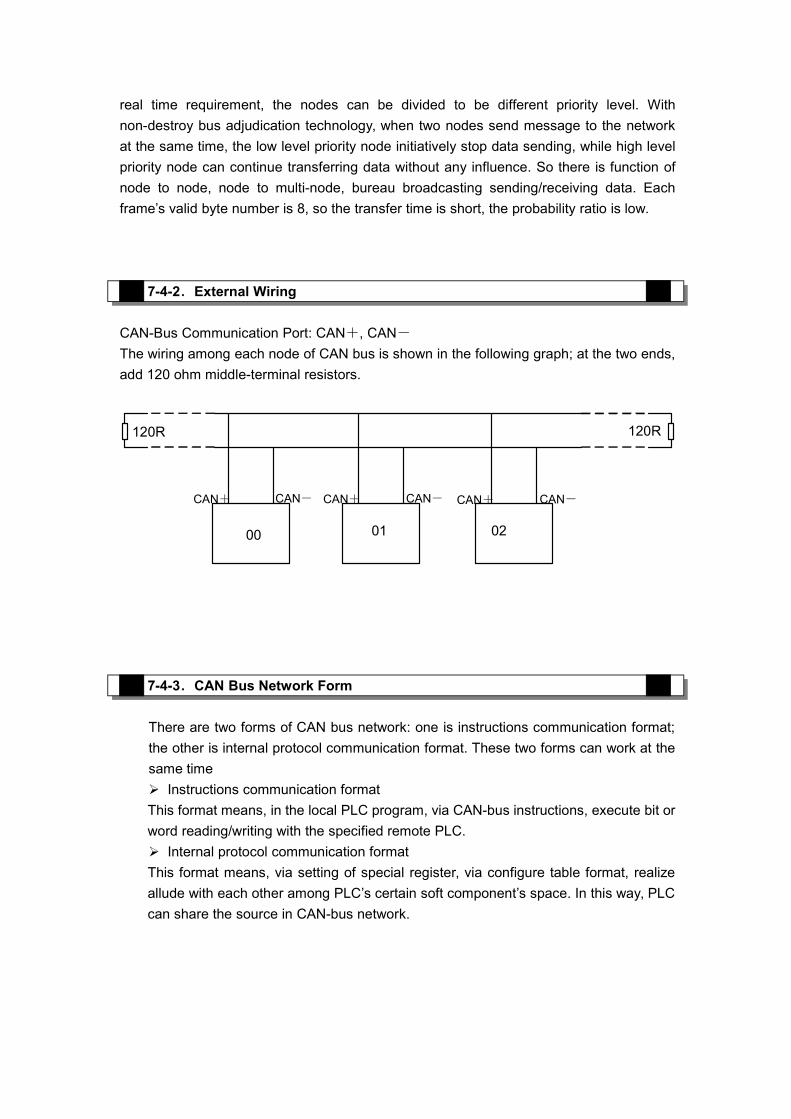
real time requirement, the nodes can be divided to be different priority level. Withnon-destroy bus adjudication technology, when two nodes send message to the networkat the same time, the low level priority node initiatively stop data sending, while high levelpriority node can continue transferring data without any influence. So there is function ofnode to node, node to multi-node, bureau broadcasting sending/receiving data. Eachframe’s valid byte number is 8, so the transfer time is short, the probability ratio is low.
7-4-2.External Wiring
CAN-Bus Communication Port: CAN+, CAN-The wiring among each node of CAN bus is shown in the following graph; at the two ends,add 120 ohm middle-terminal resistors.
7-4-3.CAN Bus Network Form
There are two forms of CAN bus network: one is instructions communication format;the other is internal protocol communication format. These two forms can work at thesame time Instructions communication formatThis format means, in the local PLC program, via CAN-bus instructions, execute bit orword reading/writing with the specified remote PLC. Internal protocol communication formatThis format means, via setting of special register, via configure table format, realizeallude with each other among PLC’s certain soft component’s space. In this way, PLCcan share the source in CAN-bus network.
120R 120R
00 01 02
CAN+ CAN- CAN+ CAN- CAN+ CAN-

7-4-4.CAN-bus Instructions
Read Coil [CCOLR]
1、Instruction DescriptionFunction: Read the specified station’s specified coil status into the local specified coil.
Read Coil [CCOLR]16 bitsinstruction
CCOLR 32 bitsinstruction
-
ExecutionCondition
Normally ON/OFF, risingedge activates
SuitableModels
XC5, XCC
HardwareRequirement
- SoftwareRequirement
-
2、OperandsOperands
Function Type
S1 Specify remote communication station no. or soft component’saddress;
16bits, BIN
S2 Specify the remote coil’s start address or soft component’saddress;
16bits, BIN
S3 Specify the coil quantity or soft component’s address; 16bits, BIND Specify the local receive coil’s start address bit
3、Suitable Soft Components
CCOLR K2 M20K20 K4
S1· S2· S3· D·X0
Word Operan
ds
System Consta
nt
Module
D FD ED TD CD DX DY DM DS K/H ID QD
S1 ● ● ● ● ●
S2 ● ● ● ● ●
S3 ● ● ● ● ●
Function
Operan
ds
System
X Y M S T C Dn.m
D ● ● ● ● ● ●
Bit
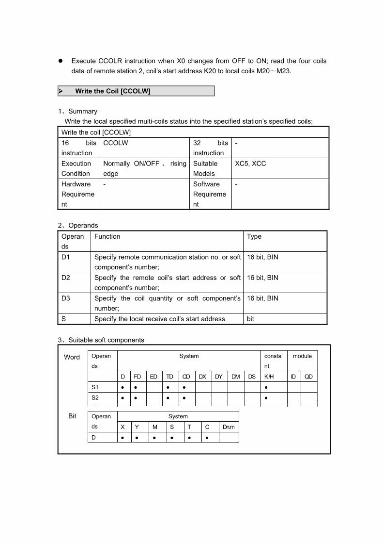
Execute CCOLR instruction when X0 changes from OFF to ON; read the four coilsdata of remote station 2, coil’s start address K20 to local coils M20~M23.
Write the Coil [CCOLW]
1、SummaryWrite the local specified multi-coils status into the specified station’s specified coils;Write the coil [CCOLW]16 bitsinstruction
CCOLW 32 bitsinstruction
-
ExecutionCondition
Normally ON/OFF 、 risingedge
SuitableModels
XC5, XCC
HardwareRequirement
- SoftwareRequirement
-
2、OperandsOperands
Function Type
D1 Specify remote communication station no. or softcomponent’s number;
16 bit, BIN
D2 Specify the remote coil’s start address or softcomponent’s number;
16 bit, BIN
D3 Specify the coil quantity or soft component’snumber;
16 bit, BIN
S Specify the local receive coil’s start address bit
3、Suitable soft components
Word Operan
ds
System consta
nt
module
D FD ED TD CD DX DY DM DS K/H ID QD
S1 ● ● ● ● ●
S2 ● ● ● ● ●
S3 ● ● ● ● ●Operan
ds
System
X Y M S T C Dn.m
D ● ● ● ● ● ●
Bit

CCOLW K2 M20K20 K4X0
S·D1· D2· D3·
Execute CCOLW instruction when X0 changes from OFF to ON; write the localM20~M23 to the remote station no.2, coil’s start address K20, coil quantity is 4.
Read Register [CREGR]
1、SummaryRead the specified station’s specified register to the local specified register;Read register [CREGR]16 bitsinstruction
CREGR 32 bits instruction -
ExecutionCondition
Normally ON/OFF、rising edge Suitable Models XC5, XCC
HardwareRequirement
- SoftwareRequirement
-
2、OperandsOperands
Function Type
D1 Specify remote communication station no. or soft component’snumber;
16bits, BIN
D2 Specify the remote register’s start address or soft component’snumber;
16bits, BIN
D3 Specify the register quantity or soft component’s number; 16bits, BINS Specify the local receive coil’s start address 16bits, BIN
3、Suitable soft components
Function
Word Operan
ds
System consta
nt
module
D FD ED TD CD DX DY DM DS K/H ID QD
S1 ● ● ● ● ●
S2 ● ● ● ● ●
S3 ● ● ● ● ●
D ● ● ●

CREGR K2 D20K20 K4
S1· S2· S3· D·X0
Execute CREGR instruction when X0 changes from OFF to ON; read the remotestation no.2, coil’s start address K20 (4 coils) to the local D20~D23
Write the Register [CREGW]
1、SummaryWrite the specified local input register to the specified station’s specified register;Write the register [CREGW]16 bitsinstruction
CREGW 32 bitsinstruction
-
ExecutionCondition
Normally ON/OFF、rising edge SuitableModels
XC5, XCC
HardwareRequirement
- SoftwareRequirement
-
2、OperandsOperands
Function Type
D1 Specify remote communication station no. or softcomponent’s number;
16bits, BIN
D2 Specify the remote register’s start address orsoft component’s number;
16bits, BIN
D3 Specify the register quantity or soft component’snumber;
16bits, BIN
S Specify the local receive coil’s start address 16bits, BIN
3、Suitable soft components
Function
Word Operan
ds
System consta
nt
module
D FD ED TD CD DX DY DM DS K/H ID QD
S1 ● ● ● ● ●
S2 ● ● ● ● ●
S3 ● ● ● ● ●
D ● ● ●
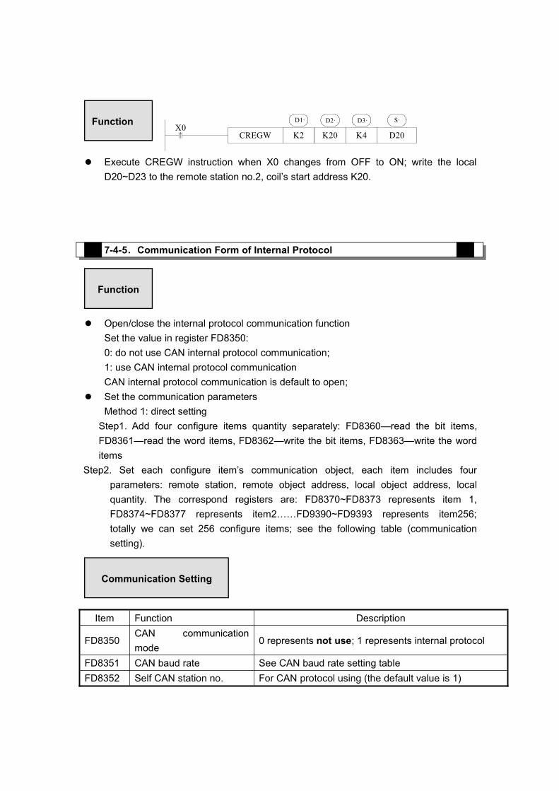
CREGW K2 D20K20 K4X0
S·D1· D2· D3·
Execute CREGW instruction when X0 changes from OFF to ON; write the localD20~D23 to the remote station no.2, coil’s start address K20.
7-4-5.Communication Form of Internal Protocol
Open/close the internal protocol communication functionSet the value in register FD8350:0: do not use CAN internal protocol communication;1: use CAN internal protocol communicationCAN internal protocol communication is default to open;
Set the communication parametersMethod 1: direct setting
Step1. Add four configure items quantity separately: FD8360—read the bit items,FD8361—read the word items, FD8362—write the bit items, FD8363—write the worditems
Step2. Set each configure item’s communication object, each item includes fourparameters: remote station, remote object address, local object address, localquantity. The correspond registers are: FD8370~FD8373 represents item 1,FD8374~FD8377 represents item2……FD9390~FD9393 represents item256;totally we can set 256 configure items; see the following table (communicationsetting).
Item Function Description
FD8350CAN communicationmode
0 represents not use; 1 represents internal protocol
FD8351 CAN baud rate See CAN baud rate setting tableFD8352 Self CAN station no. For CAN protocol using (the default value is 1)
Function
Function
Communication Setting
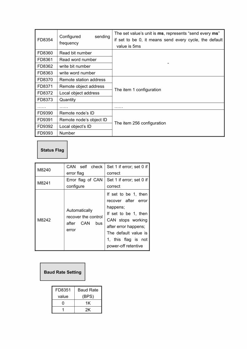
FD8354Configured sendingfrequency
The set value’s unit is ms, represents “send every ms”if set to be 0, it means send every cycle, the defaultvalue is 5ms
FD8360 Read bit number
-FD8361 Read word numberFD8362 write bit numberFD8363 write word numberFD8370 Remote station address
The item 1 configurationFD8371 Remote object addressFD8372 Local object addressFD8373 Quantity…… …… ……FD9390 Remote node’s ID
The item 256 configurationFD9391 Remote node’s object IDFD9392 Local object’s IDFD9393 Number
M8240CAN self checkerror flag
Set 1 if error; set 0 ifcorrect
M8241Error flag of CANconfigure
Set 1 if error; set 0 ifcorrect
M8242
Automaticallyrecover the controlafter CAN buserror
If set to be 1, thenrecover after errorhappens;If set to be 1, thenCAN stops workingafter error happens;The default value is1, this flag is notpower-off retentive
FD8351value
Baud Rate(BPS)
0 1K1 2K
Status Flag
Baud Rate Setting
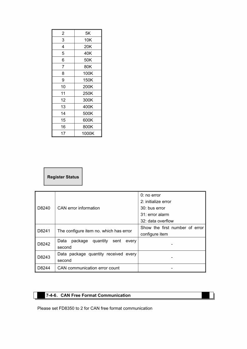
D8240 CAN error information
0: no error2: initialize error30: bus error31: error alarm32: data overflow
D8241 The configure item no. which has errorShow the first number of errorconfigure item
D8242Data package quantity sent everysecond
-
D8243Data package quantity received everysecond
-
D8244 CAN communication error count -
7-4-6.CAN Free Format Communication
Please set FD8350 to 2 for CAN free format communication
2 5K3 10K4 20K5 40K6 50K7 80K8 100K9 150K10 200K11 250K12 300K13 400K14 500K15 600K16 800K17 1000K
Register Status
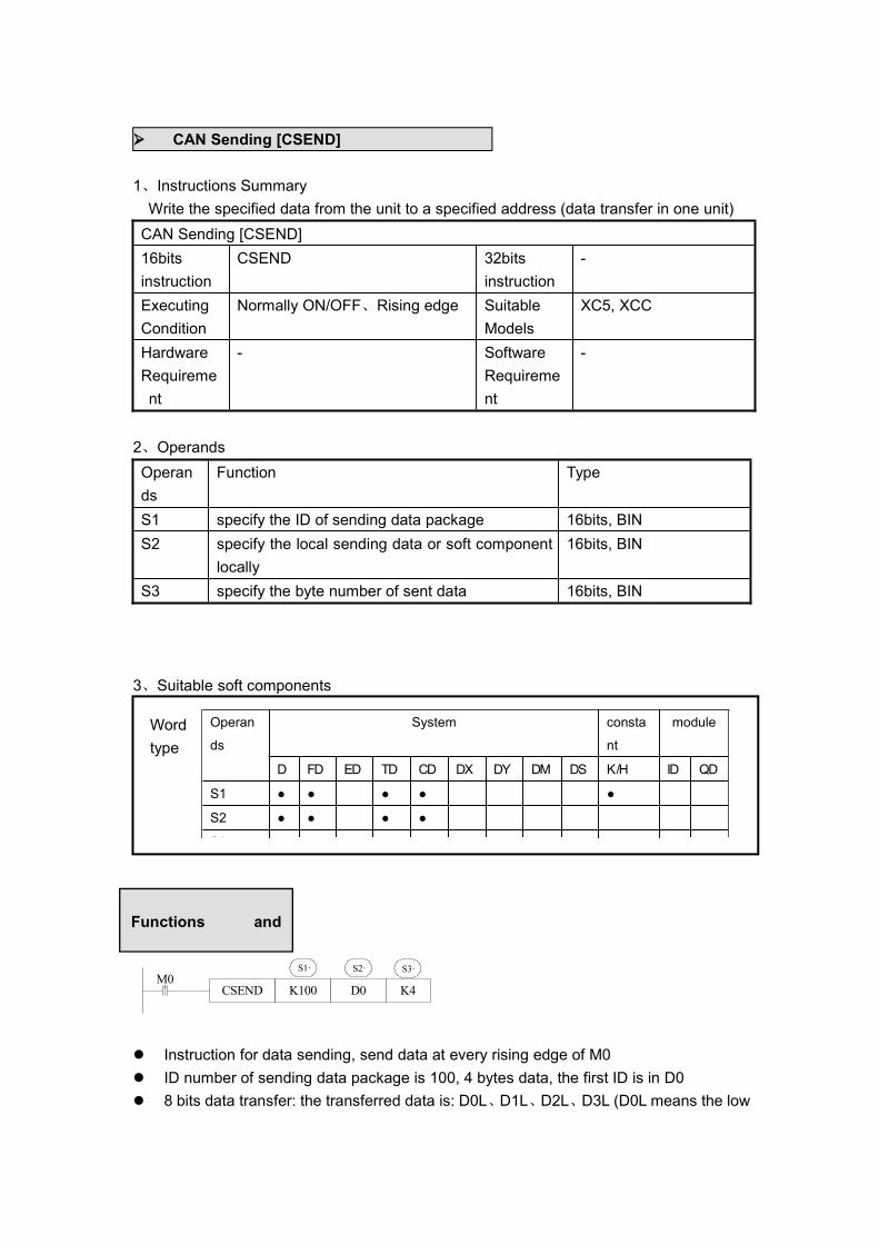
CAN Sending [CSEND]
1、Instructions SummaryWrite the specified data from the unit to a specified address (data transfer in one unit)CAN Sending [CSEND]16bitsinstruction
CSEND 32bitsinstruction
-
ExecutingCondition
Normally ON/OFF、Rising edge SuitableModels
XC5, XCC
HardwareRequirement
- SoftwareRequirement
-
2、OperandsOperands
Function Type
S1 specify the ID of sending data package 16bits, BINS2 specify the local sending data or soft component
locally16bits, BIN
S3 specify the byte number of sent data 16bits, BIN
3、Suitable soft components
CSEND K100 D0 K4
S1· S2·M0
S3·
Instruction for data sending, send data at every rising edge of M0 ID number of sending data package is 100, 4 bytes data, the first ID is in D0 8 bits data transfer: the transferred data is: D0L、D1L、D2L、D3L (D0L means the low
Wordtype
Operan
ds
System consta
nt
module
D FD ED TD CD DX DY DM DS K/H ID QD
S1 ● ● ● ● ●
S2 ● ● ● ●
S3 ● ● ● ● ●
Functions and
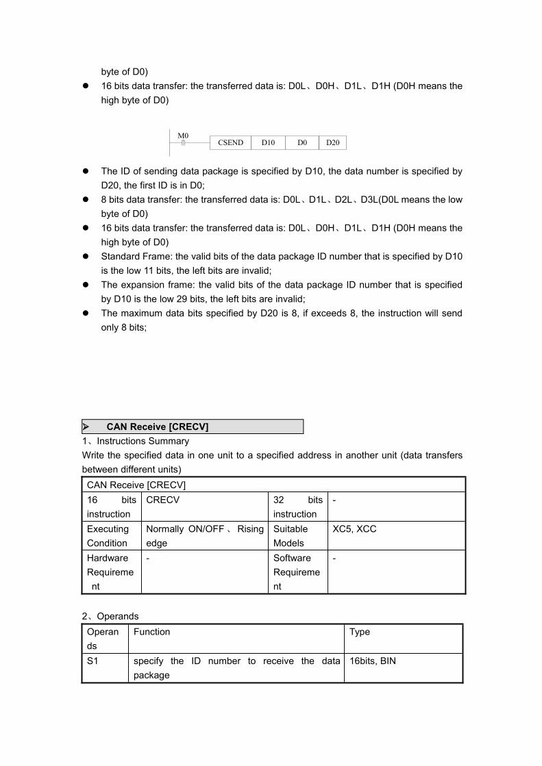
byte of D0) 16 bits data transfer: the transferred data is: D0L、D0H、D1L、D1H (D0H means the
high byte of D0)
CSEND D10 D0 D20M0
The ID of sending data package is specified by D10, the data number is specified byD20, the first ID is in D0;
8 bits data transfer: the transferred data is: D0L、D1L、D2L、D3L(D0L means the lowbyte of D0)
16 bits data transfer: the transferred data is: D0L、D0H、D1L、D1H (D0H means thehigh byte of D0)
Standard Frame: the valid bits of the data package ID number that is specified by D10is the low 11 bits, the left bits are invalid;
The expansion frame: the valid bits of the data package ID number that is specifiedby D10 is the low 29 bits, the left bits are invalid;
The maximum data bits specified by D20 is 8, if exceeds 8, the instruction will sendonly 8 bits;
CAN Receive [CRECV]1、Instructions SummaryWrite the specified data in one unit to a specified address in another unit (data transfersbetween different units)CAN Receive [CRECV]16 bitsinstruction
CRECV 32 bitsinstruction
-
ExecutingCondition
Normally ON/OFF、Risingedge
SuitableModels
XC5, XCC
HardwareRequirement
- SoftwareRequirement
-
2、OperandsOperands
Function Type
S1 specify the ID number to receive the datapackage
16bits, BIN
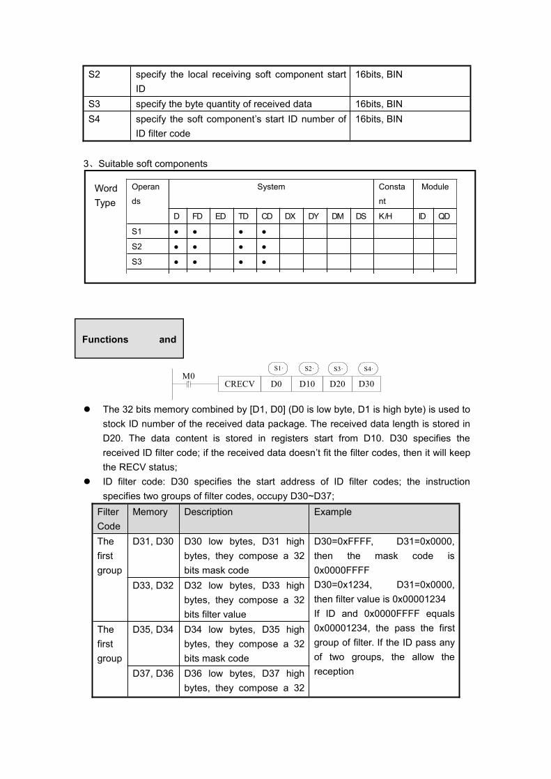
S2 specify the local receiving soft component startID
16bits, BIN
S3 specify the byte quantity of received data 16bits, BINS4 specify the soft component’s start ID number of
ID filter code16bits, BIN
3、Suitable soft components
CRECV D0 D10 D20
S1· S2·M0
S3·
D30
S4·
The 32 bits memory combined by [D1, D0] (D0 is low byte, D1 is high byte) is used tostock ID number of the received data package. The received data length is stored inD20. The data content is stored in registers start from D10. D30 specifies thereceived ID filter code; if the received data doesn’t fit the filter codes, then it will keepthe RECV status;
ID filter code: D30 specifies the start address of ID filter codes; the instructionspecifies two groups of filter codes, occupy D30~D37;
FilterCode
Memory Description Example
Thefirstgroup
D31, D30 D30 low bytes, D31 highbytes, they compose a 32bits mask code
D30=0xFFFF, D31=0x0000,then the mask code is0x0000FFFFD30=0x1234, D31=0x0000,then filter value is 0x00001234If ID and 0x0000FFFF equals0x00001234, the pass the firstgroup of filter. If the ID pass anyof two groups, the allow thereception
D33, D32 D32 low bytes, D33 highbytes, they compose a 32bits filter value
Thefirstgroup
D35, D34 D34 low bytes, D35 highbytes, they compose a 32bits mask code
D37, D36 D36 low bytes, D37 highbytes, they compose a 32
WordType
Operan
ds
System Consta
nt
Module
D FD ED TD CD DX DY DM DS K/H ID QD
S1 ● ● ● ●
S2 ● ● ● ●
S3 ● ● ● ●
S4 ●
Functions and
bits filter value Standard/ expansion frame: the setting of FD8358 has no effect to reception. If the
data frame fulfills ID mask codes, the standard frame and the expansion frames canbe all received. When receive the standard frame, the ID bits is 11, but will still occupythe 32 bits memory combined by [D1,D0]
8 bits data transfer: the transfer data is: D0L、D1L、D2L、D3L……(D0L means the lowbyte of D0)
16 bits data transfer: the transfer data is: D0L、D0H、D1L、D1H……(D0H means thehigh byte of D0)
Relate Special Soft Components List
1. System FD8000 SettingID Function Description
FD8350 CAN Mode0: not usable1: XC-CAN network2: Free format FREE
FD8351 CAN baud rate
0, 1KBPS initial value, actual is 5KBPS.1, 2KBPS initial value, actual is 5KBPS.2, 5KBPS initial value3, 10KBPS initial value4, 20KBPS initial value5, 40KBPS initial value6, 50KBPS initial value7, 80KBPS initial value8, 100KBPS initial value9, 150KBPS initial value10, 200KBPS initial value11, 250KBPS initial value12, 300KBPS initial value13, 400KBPS initial value14, 500KBPS initial value15, 600KBPS initial value16, 800KBPS initial value17, 1000KBPS initial value
FD8358CAN free formatmode
low 8 bits: 0-standard frame .low 8 bits: 1-expansion framehigh 8 bits: 0-8 bits data storehigh 8 bits: 1-16 bits data store
FD8359CAN accepttimeout time
for free format using, unit: ms
CAN send fixed to be 5ms

timeout time
2. System M8000 flagID Function Description
M8240 CAN error flag
ON: error happensOFF: normalif set M8242 as ON, and manually setM8240 as ON, this will enable CAN reset
M8241CAN node dropped offflag
XC-CAN mode validON: certain node/nodes are dropped offOFF: Normal
M8242do reset or not if CANerror happens
ON: CAN reset automatically when errorhappensOFF: take no operation when error happens
M8243CAN send/acceptfinished flag
FREE mode validON: receive/accept finishreset ON automatically when starting tosend/accept
M8244CAN send/accepttimeout flag
FREE mode validON: send/accept timeoutSet OFF automatically when starting tosend/accept
3. System D8000ID Function Description
D8240 CAN error information
0: no error2: initializing error30: CAN bus error31: error alarm32: data overflow
D8241configure item numberwhen error happens
XC-CAN valid
D8242data package number sentevery second
both XC-CAN and FREE modes arevalid
D8243data package numberaccepted every second
both XC-CAN and FREE modes arevalid
D8244CAN communication errorcounter
correspond with M8240at every CAN error, M8240 will beset ON one time, D8244 increase 1
Note: when D8240 is not zero, please try the follow operations:1. Check the wiring2. Decrease baud rate or increase sending frequency
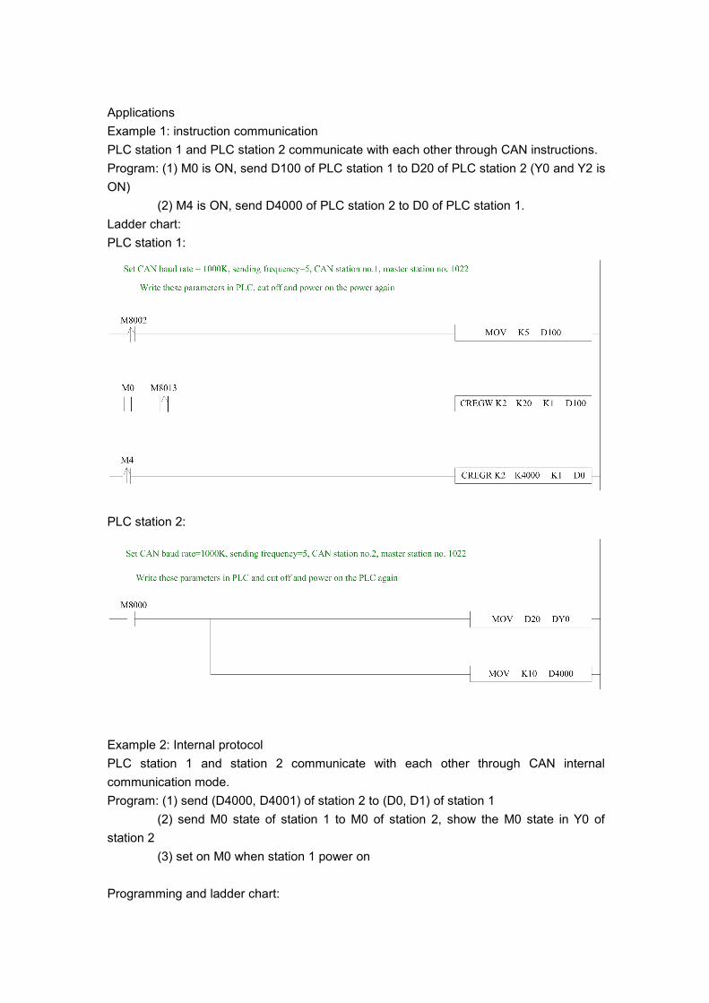
ApplicationsExample 1: instruction communicationPLC station 1 and PLC station 2 communicate with each other through CAN instructions.Program: (1) M0 is ON, send D100 of PLC station 1 to D20 of PLC station 2 (Y0 and Y2 isON)
(2) M4 is ON, send D4000 of PLC station 2 to D0 of PLC station 1.Ladder chart:PLC station 1:
PLC station 2:
Example 2: Internal protocolPLC station 1 and station 2 communicate with each other through CAN internalcommunication mode.Program: (1) send (D4000, D4001) of station 2 to (D0, D1) of station 1
(2) send M0 state of station 1 to M0 of station 2, show the M0 state in Y0 ofstation 2
(3) set on M0 when station 1 power on
Programming and ladder chart:
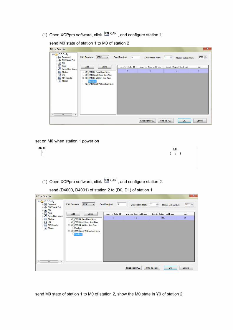
(1) Open XCPpro software, click , and configure station 1.
send M0 state of station 1 to M0 of station 2
set on M0 when station 1 power on
(1) Open XCPpro software, click , and configure station 2.
send (D4000, D4001) of station 2 to (D0, D1) of station 1
send M0 state of station 1 to M0 of station 2, show the M0 state in Y0 of station 2

Example 3: Free format (please set FD8350 to 2 first)Two Spectra PLCs communicate with each other through CAN free format modeProgram: (1) PLC station 1 sends the data package ID100 (4 bytes starts from D4000)every 1s
(2) When M0 is ON, PLC station 2 receives data package ID100 (4 bytes, ID filtercode is defaulted), then save the data in register starts from D4000.
Ladder chart:PLC station 1:
PLC station 2:

8 PID Control Function
8 PID Control Function
In this chapter, we mainly introduce the applications of PID instructions for XC series PLCbasic units, including: call the instructions, set the parameters, items to notice, sampleprograms etc.
8-1. Brief Introduction of the Functions
8-2. Instruction Formats
8-7. Sample Programs
8-5. Advanced Mode
8-6.Application Outlines
8-4. Auto Tune Mode
8-3. Parameter Setting

8 PID Control Function
8-1.Brief Introductions of the Functions
PID instruction and auto tune function are added into XC series PLC basic units (Version3.0 and above). Via auto tune method, users can get the best sampling time and PIDparameters and improve the control precision.
The previous versions can not support PID function on basic units unless they extendanalog module or BD cards. PID instruction has brought many facilities to the users. The output can be data form D and on-off quantity Y, user can choose them freelywhen program. Via auto tune, users can get the best sampling time and PID parameters and improvethe control precision. User can choose positive or negative action via software setting. The former is usedto heating control; the latter is used to cooling control. PID control separates the basic units with the expansions; this improves the flexibilityof this function. A new PID algorithm-critical oscillation is added in v3.3 and higher version of PLC.
For temperature control object:Step response method: the PID auto tune will start when current temperature of object isequal to ambient temperature.Critical oscillation method: the PID auto tune will start at any temperature.
8-2.Instruction Forms
1、Brief Introductions of the InstructionsExecute PID control instructions with the data in specified registers.PID control [PID]16 bitsinstruction
PID 32 bitsinstruction
-
ExecutingCondition
Normally ON/normallyclosed coil activates
SuitableModels
XC2, XC3, XC5, XCM, XCC
HardwareCondition
V3.0 or above SoftwareCondition
V3.0 or aboveV3.3a and above (criticaloscillation)
V3.3f and above (criticaloscillation)
2、OperandsOperands
Usage Type
S1 set the address of the target value (SV) 16bits, BIN

8 PID Control Function
S2 set the address of the tested value (PV) 16 bits, BINS3 set the start address of the control parameters 16 bits, BIND the address of the operation result (MV) or output
port16 bits, BIN; bit
3、Suitable soft components
PID D0 D10 D4000 D100X0
D·S1· S2· S3·
PID D0 D10 D4000 Y0X0
D·S1· S2· S3·
S3~ S3+ 43 will be occupied by this instruction, so please don’t use them as thecommon data registers.
This instruction executes when each sampling time interval comes.
To the operation result D, the data registers are used to store PID output values;the output points are used to output the occupy space ratio in the form ofON/OFF.
PID control rules are shown as below:
Operan
ds
System
X Y M S T C Dn.m
D ● ● ● ● ●
Word
Type
Functions andActions
Bit
Type
Operan
ds
System Consta
nt
Module
D FD ED TD CD DX DY DM DS K/H ID QD
S1 ● ●
S2 ● ●
S3 ●
D ● ●
u(t)
c (t)r (t) + e (t)
Proportion
Integral
Differential
Be controlledobject
+
+
+
-
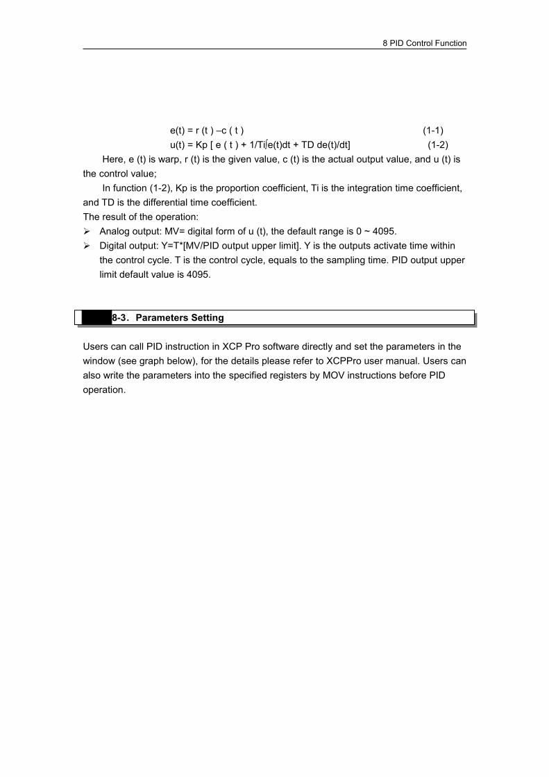
8 PID Control Function
e(t) = r (t ) –c ( t ) (1-1)u(t) = Kp [ e ( t ) + 1/Ti∫e(t)dt + TD de(t)/dt] (1-2)
Here, e (t) is warp, r (t) is the given value, c (t) is the actual output value, and u (t) isthe control value;
In function (1-2), Kp is the proportion coefficient, Ti is the integration time coefficient,and TD is the differential time coefficient.The result of the operation: Analog output: MV= digital form of u (t), the default range is 0 ~ 4095. Digital output: Y=T*[MV/PID output upper limit]. Y is the outputs activate time within
the control cycle. T is the control cycle, equals to the sampling time. PID output upperlimit default value is 4095.
8-3.Parameters Setting
Users can call PID instruction in XCP Pro software directly and set the parameters in thewindow (see graph below), for the details please refer to XCPPro user manual. Users canalso write the parameters into the specified registers by MOV instructions before PIDoperation.
8 PID Control Function
Auto tune mode:

8 PID Control Function
V3.3f and higher version software can choose auto tune mode: step response or criticaloscillation.
8-3-1.Registers and their functions
For PID control instruction’s relative parameters ID, please refer to the below table:ID Function Description MemoS3 sampling time 32 bits without sign Unit: msS3+1 sampling time 32 bits without sign Unit: msS3+2 mode setting bit0:
0: Negative action; 1 positiveaction;bit1~bit6 not usablebit7:0: Manual PID; 1: auto tune PIDbit8:

8 PID Control Function
1: auto tune successful flagbit9~bit10 auto tune method00: step response01: critical oscillationBit11~bit12: not useBit13~bit14: auto tune PIDmode(valid in critical oscillationmode)00: PID control01: PI control10: P controlbit15:0: regular mode; 1: advancedmode
S3+3 Proportion Gain(Kp)
Range: 1~32767[%]
S3+4 Integration time (TI) 0~32767[*100ms] 0 is taken as no integral.S3+5 Differential time
(TD)0~32767[*10ms] 0 is taken as no
differential.S3+6 PID operation zone 0~32767 PID adjustment band
width value.S3+7 control death zone 0~32767 PID value keeps constant
in death zoneS3+8 PID auto tune cycle
varied valuefull scale AD value * (0.3~1%)
S3+9 PID auto tuneovershootpermission
0: enable overshoot1:not overshoot
(valid when using stepresponse method)
S3+10 current target valueadjustment percentin auto tunefinishing transitionstage
S3+11 current target valueresident count inauto tune finishingtransition stage
S3+12~S3+39
occupied by PIDoperation’s internalprocess
Below is the ID of advanced PID mode settingS3+40 Input filter constant (a) 0~99[%] 0: no input filterS3+41 Differential gain (KD) 0~100[%] 0: no differential gain
8 PID Control Function
S3+42 Output upper limitvalue
-32767~32767
S3+43 Output lower limitvalue
-32767~32767
8-3-2.Parameters Description
Movement Direction:
Positive movement: the output value MV will increase with the increasing of thedetected value PV, usually used for cooling control.
Negative movement: the output value MV will decrease with the increasing of thedetected value PV, usually used for heating control.
Mode Setting
Common Mode:The parameter’s register zone is from S3 to S3+43, S3 to S3+11 needs to be set byusers. S3+12 to S3+43+12 are occupied by the system, users can’t use them.
Advanced ModeThe parameter’s register zone is from S3 to S3+43, S3 to (S3+11) and (S3+40) to(S3+43) need to be set by users. (S3+12) to (S3+39) are occupied by the system,users can’t use them.
Sample Time [S3]
The system collected the current value according to the certain time interval andcompared them with the output value. This time interval is the sample time T. There isno requirement for T during AD output. T should be larger than one PLC scan periodduring port output. T value should be chosen among 100~1000 times of PLC scanperiods.
PID Operation Zone [S3+6]
PID control is entirely opened at the beginning and close to the target value with thehighest speed (the defaulted value is 4095), when it entered into the PID computationrange, parameters Kp, Ti, TD will be effective.See graph below:
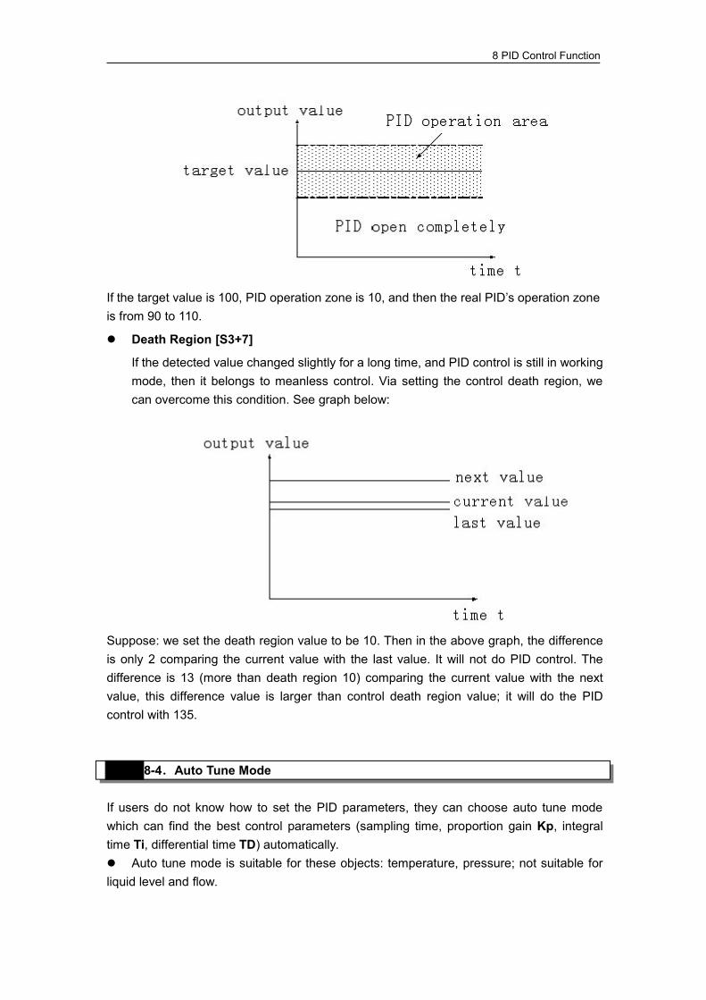
8 PID Control Function
If the target value is 100, PID operation zone is 10, and then the real PID’s operation zoneis from 90 to 110.
Death Region [S3+7]
If the detected value changed slightly for a long time, and PID control is still in workingmode, then it belongs to meanless control. Via setting the control death region, wecan overcome this condition. See graph below:
Suppose: we set the death region value to be 10. Then in the above graph, the differenceis only 2 comparing the current value with the last value. It will not do PID control. Thedifference is 13 (more than death region 10) comparing the current value with the nextvalue, this difference value is larger than control death region value; it will do the PIDcontrol with 135.
8-4.Auto Tune Mode
If users do not know how to set the PID parameters, they can choose auto tune modewhich can find the best control parameters (sampling time, proportion gain Kp, integraltime Ti, differential time TD) automatically. Auto tune mode is suitable for these objects: temperature, pressure; not suitable forliquid level and flow.
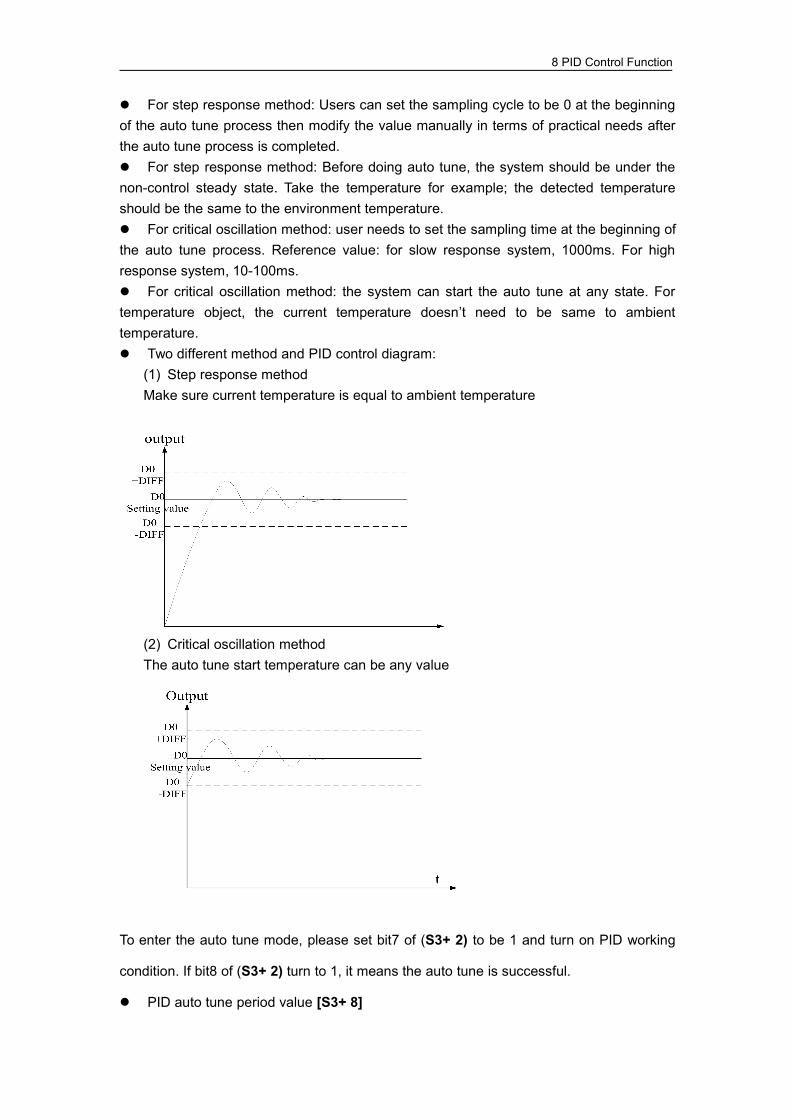
8 PID Control Function
For step response method: Users can set the sampling cycle to be 0 at the beginningof the auto tune process then modify the value manually in terms of practical needs afterthe auto tune process is completed. For step response method: Before doing auto tune, the system should be under thenon-control steady state. Take the temperature for example; the detected temperatureshould be the same to the environment temperature. For critical oscillation method: user needs to set the sampling time at the beginning ofthe auto tune process. Reference value: for slow response system, 1000ms. For highresponse system, 10-100ms. For critical oscillation method: the system can start the auto tune at any state. Fortemperature object, the current temperature doesn’t need to be same to ambienttemperature. Two different method and PID control diagram:
(1) Step response methodMake sure current temperature is equal to ambient temperature
(2) Critical oscillation methodThe auto tune start temperature can be any value
To enter the auto tune mode, please set bit7 of (S3+ 2) to be 1 and turn on PID working
condition. If bit8 of (S3+ 2) turn to 1, it means the auto tune is successful.
PID auto tune period value [S3+ 8]

8 PID Control Function
Set this value in [S3+ 8] during auto tune.This value decides the auto tune performance, in a general way, set this value to be theAD result corresponding to one standard detected unit. The default value is 10. Thesuggested setting range:full-scale AD result × 0.3 ~ 1%.User doesn’t need to change this value. However, if the system is interfered greatly byoutside, this value should be increased modestly to avoid wrong judgment for positive ornegative movement. If this value is too large, the PID control period (sampling time) gotfrom the auto tune process will be too long. As the result do not set this value too large.
※1: if users have no experience, please use the defaulted value 10, set PID samplingtime (control period) to be 0ms then start the auto tune.
PID auto tune overshooting permission setting [S3+ 9]If set 0, overshooting is permitted, the system can study the optimal PID parameters allthe time. But in auto tune process, detected value may be lower or higher than the targetvalue, safety factor should be considered here.
If set 1, overshooting is not permitted. For these objectives which have strict safety
demand such as pressure vessel, set [S3+ 9] to be 1 to prevent from detected value
seriously over the target value. In this process, if [S3+ 2] bit8 changes from 0 to 1, it
means the auto tune is successful and the optimal parameters are got; if [S3+ 2] is always
0 until [S3+ 2] bit7 changes from 1 to 0, it means the auto tune is completed but the
parameters are not the best and need to be modified by users.
Every adjustment percent of current target value at auto tune process finishing
transition stage [S3+10]
This parameter is effective only when [S3+ 9] is 1.
If doing PID control after auto tune, small range of overshooting may be occurred. It is
better to decrease this parameter to control the overshooting. But response delay may
occur if this value is too small. The defaulted value is 100% which means the parameter is
not effective. The recommended range is 50~80%.
Cutline Explanation:Current target value adjustment percent is 2/3 (S3 + 10 = 67%), the original temperatureof the system is 0 ºC, target temperature is 100 ºC, and the current target temperatureadjustment situation is shown as below:
Next current target value = current target value + (final target value – current target value)
× 2/3;
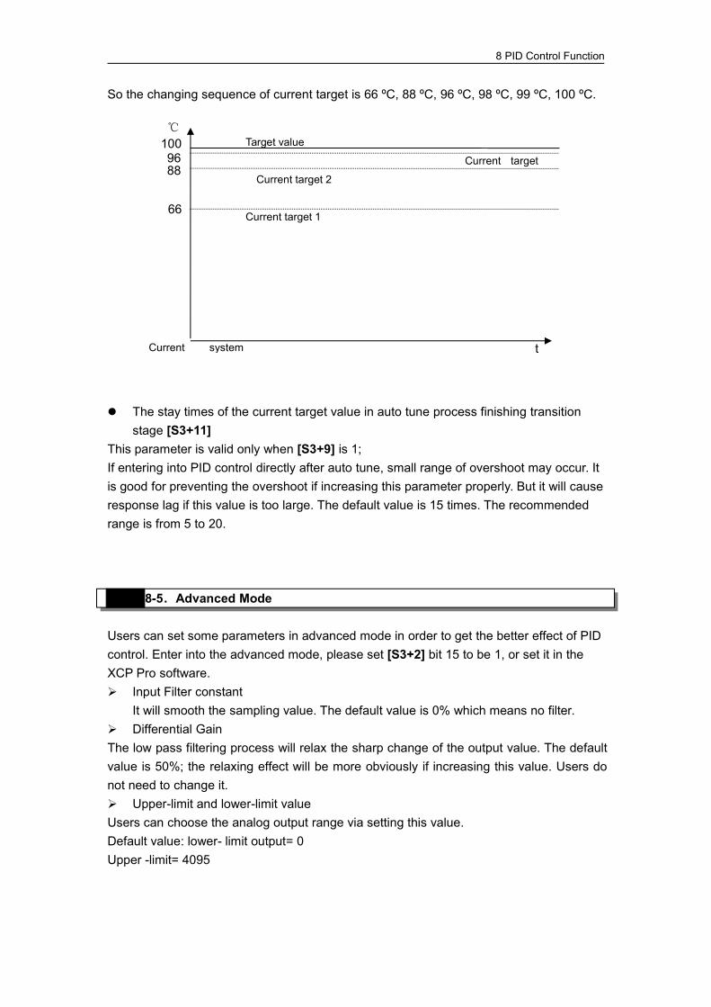
8 PID Control Function
So the changing sequence of current target is 66 ºC, 88 ºC, 96 ºC, 98 ºC, 99 ºC, 100 ºC.
The stay times of the current target value in auto tune process finishing transitionstage [S3+11]
This parameter is valid only when [S3+9] is 1;If entering into PID control directly after auto tune, small range of overshoot may occur. Itis good for preventing the overshoot if increasing this parameter properly. But it will causeresponse lag if this value is too large. The default value is 15 times. The recommendedrange is from 5 to 20.
8-5.Advanced Mode
Users can set some parameters in advanced mode in order to get the better effect of PIDcontrol. Enter into the advanced mode, please set [S3+2] bit 15 to be 1, or set it in theXCP Pro software. Input Filter constant
It will smooth the sampling value. The default value is 0% which means no filter. Differential GainThe low pass filtering process will relax the sharp change of the output value. The defaultvalue is 50%; the relaxing effect will be more obviously if increasing this value. Users donot need to change it. Upper-limit and lower-limit valueUsers can choose the analog output range via setting this value.Default value: lower- limit output= 0Upper -limit= 4095
℃
t
1009688
66
Current system
Current target
Current target 2
Current target 1
Target value
8 PID Control Function
8-6.Application Outlines
Under the circumstances of continuous output, the system whose effect ability will diedown with the change of the feedback value can do self-study, such as temperatureor pressure. It is not suitable for flux or liquid level.
Under the condition of overshoot permission, the system will get the optimal PIDparameters from self-study.
Under the condition of overshoot not allowed, the PID parameters got from self-studyis up to the target value, it means that different target value will produce different PIDparameters which are not the optimal parameters of the system and for referenceonly.
If the self-study is not available, users can set the PID parameters according topractical experience. Users need to modify the parameters when debugging. Beloware some experience values of the control system for your reference:
8-7.Application
PID Control Program is shown below:
Temperature system:P (%) 2000 ~ 6000, I (minutes) 3 ~ 10, D (minutes) 0.5 ~ 3 Flux system: P (%) 4000 ~ 10000, I (minutes) 0.1 ~ 1 Pressure system: P (%) 3000 ~ 7000, I (minutes) 0.4 ~
3 Liquid level system: P (%) 2000 ~ 8000, I (minutes) 1 ~
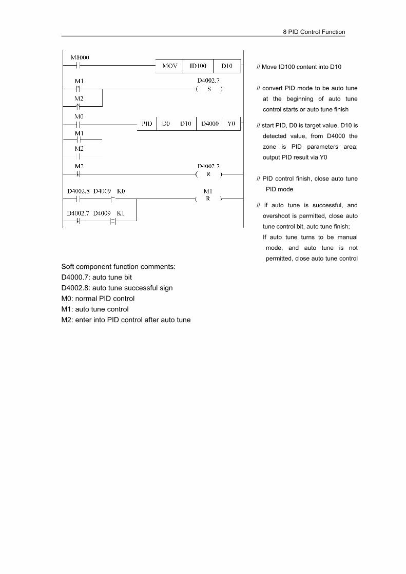
8 PID Control Function
Soft component function comments:D4000.7: auto tune bitD4002.8: auto tune successful signM0: normal PID controlM1: auto tune controlM2: enter into PID control after auto tune
// Move ID100 content into D10
// convert PID mode to be auto tune
at the beginning of auto tune
control starts or auto tune finish
// start PID, D0 is target value, D10 is
detected value, from D4000 the
zone is PID parameters area;
output PID result via Y0
// PID control finish, close auto tune
PID mode
// if auto tune is successful, and
overshoot is permitted, close auto
tune control bit, auto tune finish;
If auto tune turns to be manual
mode, and auto tune is not
permitted, close auto tune control
bit

10 Sequence Block
9 C Function Block
In this chapter, we focus on C language function block’s specifications, edition, instructioncalling, application points etc. we also attach the common Function list.
9-1.Functions Summary
9-2.Instrument Form
9-3.Operation Steps
9-4.Import and Export of the Functions
9-5.Edit the Function Block
9-6.Example Program
9-7.Application Points
9-8.Function List
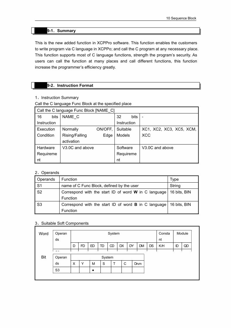
10 Sequence Block
9-1.Summary
This is the new added function in XCPPro software. This function enables the customersto write program via C language in XCPPo; and call the C program at any necessary place.This function supports most of C language functions, strength the program’s security. Asusers can call the function at many places and call different functions, this functionincrease the programmer’s efficiency greatly.
9-2.Instruction Format
1、Instruction SummaryCall the C language Func Block at the specified placeCall the C language Func Block [NAME_C]16 bitsInstruction
NAME_C 32 bitsInstruction
-
ExecutionCondition
Normally ON/OFF,Rising/Falling Edgeactivation
SuitableModels
XC1, XC2, XC3, XC5, XCM,XCC
HardwareRequirement
V3.0C and above SoftwareRequirement
V3.0C and above
2、OperandsOperands Function TypeS1 name of C Func Block, defined by the user StringS2 Correspond with the start ID of word W in C language
Function16 bits, BIN
S3 Correspond with the start ID of word B in C languageFunction
16 bits, BIN
3、Suitable Soft Components
Operan
ds
System
X Y M S T C Dn.m
S3 ●
Word
Bit
Operan
ds
System Consta
nt
Module
D FD ED TD CD DX DY DM DS K/H ID QD
S2 ●
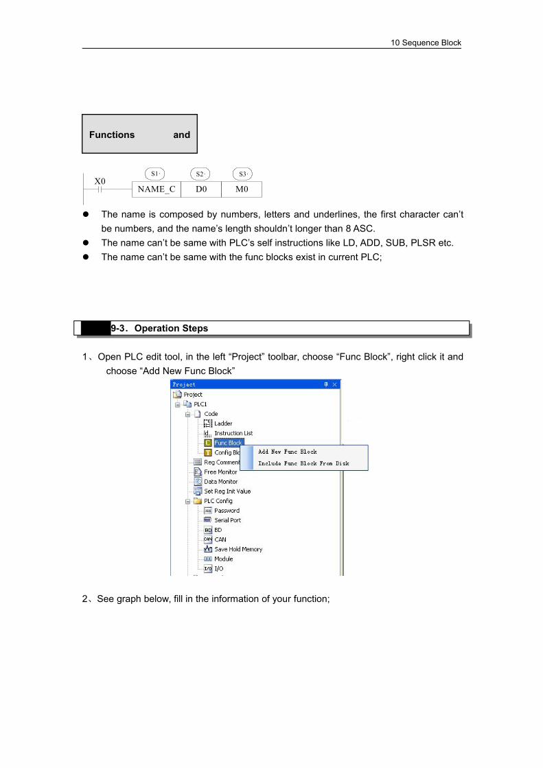
10 Sequence Block
NAME_C D0 M0X0
S1· S2· S3·
The name is composed by numbers, letters and underlines, the first character can’tbe numbers, and the name’s length shouldn’t longer than 8 ASC.
The name can’t be same with PLC’s self instructions like LD, ADD, SUB, PLSR etc. The name can’t be same with the func blocks exist in current PLC;
9-3.Operation Steps
1、Open PLC edit tool, in the left “Project” toolbar, choose “Func Block”, right click it andchoose “Add New Func Block”
2、See graph below, fill in the information of your function;
Functions and

10 Sequence Block
3、After new create the Func Block, you can see the edit interface as shown below:
Parameters’ transfer format: if call the Func Block in ladder, the transferred D and Mis the start ID of W and B. Take the above graph as the example, start with D0 and M0,then W[0] is D0, W[10] is D10, B[0 is M0, B[10]is M10. If in the ladder the usedparameters are D100, M100, then W[0] is D100, B[0] is M100. So, word and bitcomponent’s start address is defined in PLC program by the user.
Parameter W: represent Word soft component, use in the form of data group. E.g. W[0] =1; W [1] =W [2] +W [3]; in the program, use according to standard C languagerules.
Edit your C languageprogram between “{}”
Main function’s name (it’s function block’sname, this name can’t be changed freely,and users should modify in the edit window.
WORD W: correspond with soft component DBIT B: correspond with soft component M
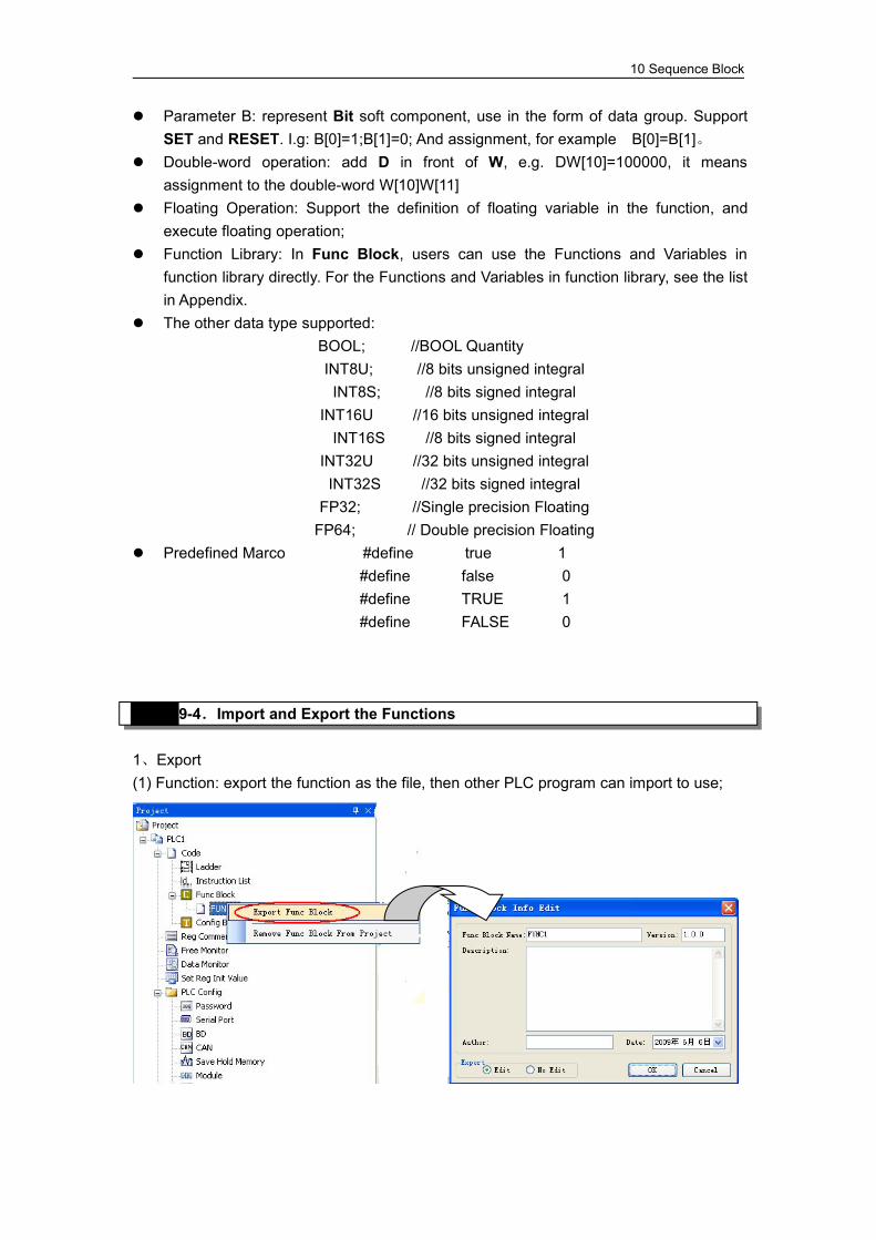
10 Sequence Block
Parameter B: represent Bit soft component, use in the form of data group. SupportSET and RESET. I.g: B[0]=1;B[1]=0; And assignment, for example B[0]=B[1]。
Double-word operation: add D in front of W, e.g. DW[10]=100000, it meansassignment to the double-word W[10]W[11]
Floating Operation: Support the definition of floating variable in the function, andexecute floating operation;
Function Library: In Func Block, users can use the Functions and Variables infunction library directly. For the Functions and Variables in function library, see the listin Appendix.
The other data type supported:BOOL; //BOOL QuantityINT8U; //8 bits unsigned integralINT8S; //8 bits signed integral
INT16U //16 bits unsigned integralINT16S //8 bits signed integral
INT32U //32 bits unsigned integralINT32S //32 bits signed integral
FP32; //Single precision FloatingFP64; // Double precision Floating
Predefined Marco #define true 1#define false 0#define TRUE 1#define FALSE 0
9-4.Import and Export the Functions
1、Export(1) Function: export the function as the file, then other PLC program can import to use;
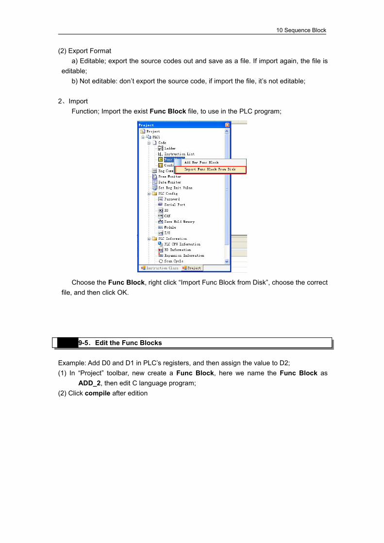
10 Sequence Block
(2) Export Formata) Editable; export the source codes out and save as a file. If import again, the file is
editable;b) Not editable: don’t export the source code, if import the file, it’s not editable;
2、ImportFunction; Import the exist Func Block file, to use in the PLC program;
Choose the Func Block, right click “Import Func Block from Disk”, choose the correctfile, and then click OK.
9-5.Edit the Func Blocks
Example: Add D0 and D1 in PLC’s registers, and then assign the value to D2;(1) In “Project” toolbar, new create a Func Block, here we name the Func Block as
ADD_2, then edit C language program;(2) Click compile after edition
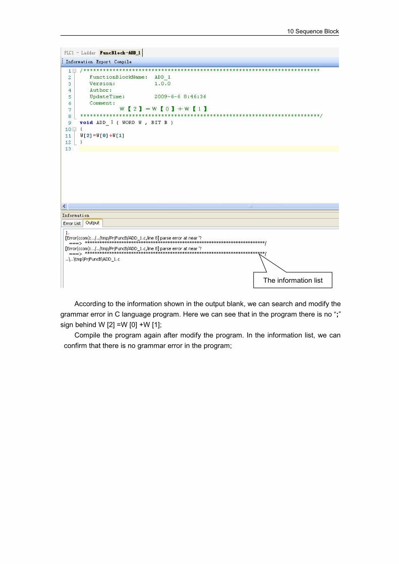
10 Sequence Block
According to the information shown in the output blank, we can search and modify thegrammar error in C language program. Here we can see that in the program there is no “;”sign behind W [2] =W [0] +W [1];
Compile the program again after modify the program. In the information list, we canconfirm that there is no grammar error in the program;
The information list
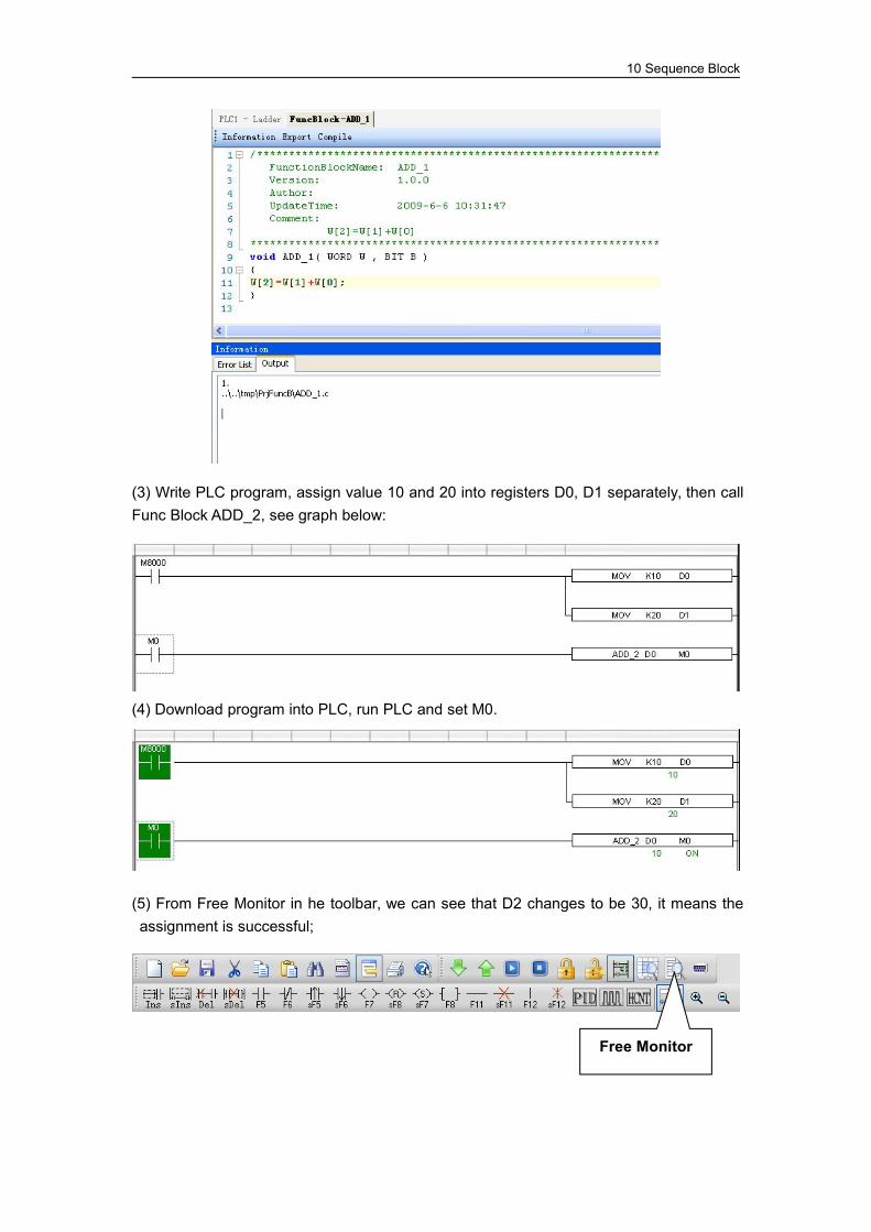
10 Sequence Block
(3) Write PLC program, assign value 10 and 20 into registers D0, D1 separately, then callFunc Block ADD_2, see graph below:
(4) Download program into PLC, run PLC and set M0.
(5) From Free Monitor in he toolbar, we can see that D2 changes to be 30, it means theassignment is successful;
Free Monitor

10 Sequence Block
9-6.Program Example
If PLC needs to do complicated calculation (including plus and minus calculation), thecalculation will be used for many times, C language function is easy to use.
Example 1:Calculation a=b/c+b*c+(c-3)*d.Method 1: use ladder chart: Get the result of c-3 Get the result of three multiplication equations Get the sumLadder chart only support two original operands, it needs many steps to get the result.
Note:1. The result of MUL is Dword, the result is stored in D14~D15.2. The result of DIV has quotient D16 and remainder D17. If D17 has value, the
calculation precision will decrease. Please use float format to ensure theprecision.
3. D16 quotient is word value, in plus calculation all the data should be changed toDword. The final result is stored in D22~D23.

10 Sequence Block
Method 2: use C languageLadder chart:
C program:
RESULT Function nameD0 In the function, W [0] =D0, W [1] =D1….
If S2=D32, then W [0] =D32, W [1] =D33….M0 In the function, B [0] =M0, B [1] =M1…..
If S2=M32, then B [0] =M32, B [1] =M33….
Method 2 can simplify the program.The C function is the same to ladder chart of method 1. The precision is not high. If itneeds to get the high precision, please use float calculation.
Example 2:Calculate CRC parity value via Func Block CRC calculation rules:(1) Set 16 bits register (CRC register) = FFFF H XOR (Exclusive OR) 8 bits information with the low byte of the 16 bits CRC register. Right shift 1 bit of CRC register, fill 0 in the highest bit. Check the right shifted value, if it is 0, save the new value from step3 into CRCregister; if it is not 0, XOR the CRC register value with A001 H and save the result into theCRC register. Repeat step3&4 until all the 8 bits have been calculated. Repeat step2~5, then calculate the next 8 bits information. Until all the informationhas been calculated, the result will be the CRC parity code in CRC register.
Edit C language Function Block program, see graph below:
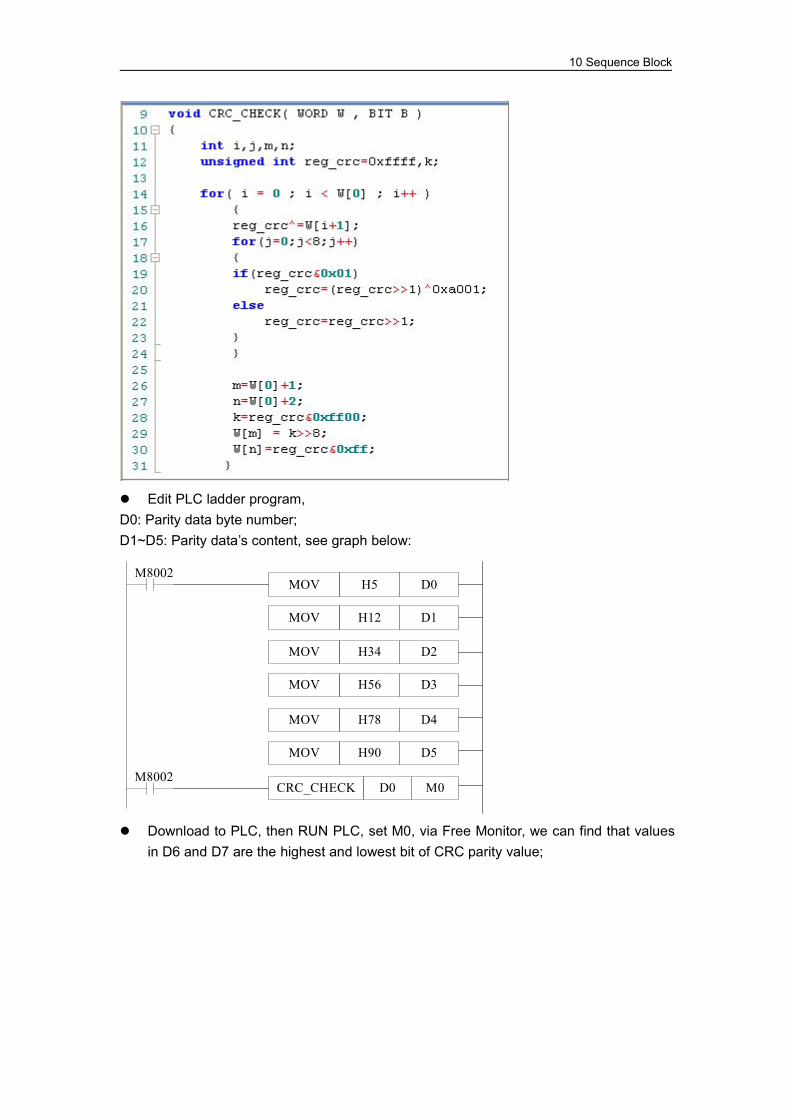
10 Sequence Block
Edit PLC ladder program,D0: Parity data byte number;D1~D5: Parity data’s content, see graph below:
MOV H5 D0M8002
MOV H12 D1
MOV H34 D2
MOV H56 D3
MOV H78 D4
MOV H90 D5
CRC_CHECK D0 M0M8002
Download to PLC, then RUN PLC, set M0, via Free Monitor, we can find that valuesin D6 and D7 are the highest and lowest bit of CRC parity value;
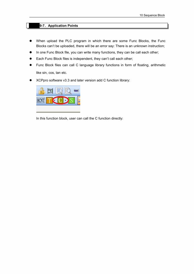
10 Sequence Block
9-7.Application Points
When upload the PLC program in which there are some Func Blocks, the FuncBlocks can’t be uploaded, there will be an error say: There is an unknown instruction;
In one Func Block file, you can write many functions, they can be call each other;
Each Func Block files is independent, they can’t call each other;
Func Block files can call C language library functions in form of floating, arithmetic
like sin, cos, tan etc.
XCPpro software v3.3 and later version add C function library:
In this function block, user can call the C function directly:
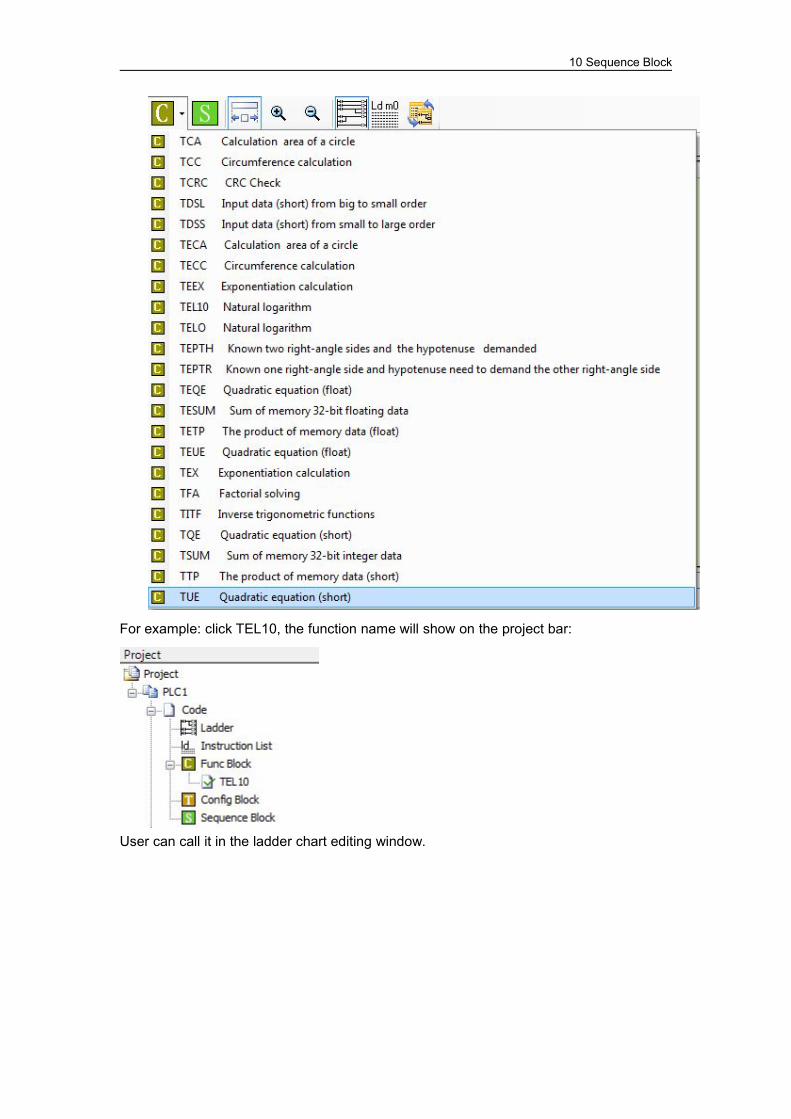
10 Sequence Block
For example: click TEL10, the function name will show on the project bar:
User can call it in the ladder chart editing window.

10 Sequence Block
9-8.Function Table
The default function libraryConstant Data Description_LOG2 (double)0.693147180559945309417232121458 Logarithm of 2_LOG10 (double)2.3025850929940459010936137929093 Logarithm of 10_SQRT2 (double)1.41421356237309504880168872421 Radical of 2
_PI (double)3.1415926535897932384626433832795 PI_PIP2 (double)1.57079632679489661923132169163975 PI/2_PIP2x3 (double)4.71238898038468985769396507491925 PI*3/2
String Function Description
void * memchr(const void *s, int c, size_t n);Return the first c position amongn words before s position
int memcmp(const void *s1, const void *s2,size_t n);
Compare the first n words ofposition s1 and s2
void * memcpy(void *s1, const void *s2, size_t n);Copy n words from position s2 tos1and return s1
void * memset(void *s, int c, size_t n);Replace the n words start from sposition with word c, and returnposition s
char * strcat(char *s1, const char *s2); Connect string ct behind string s
char * strchr(const char *s, int c);Return the first word c position instring s
int strcmp(const char *s1, const char *s2); Compare string s1 and s2char * strcpy(char *s1, const char *s2); Copy string s1 to string s2
Double-precision mathfunction
Single-precision mathfunction
Description
double acos(double x); float acosf(float x); Inverse cosine function.double asin(double x); float asinf(float x); Inverse sine functiondouble atan(double x); float atanf(float x); Inverse tangent functiondouble atan2(double y,double x);
float atan2f(float y, floatx);
Inverse tangent value ofparameter (y/x)
double ceil(double x); float ceilf(float x);Return the smallest doubleintegral which is greater orequal with parameter x
double cos(double x); float cosf(float x); Cosine function
double cosh(double x); float coshf(float x);Hyperbolic cosine functioncosh(x)=(e^x+e^(-x))/2.
double exp(double x); float expf(float x); Exponent (e^x) of a nature datadouble fabs(double x); float fabsf(float x); Absolute value of parameter x
10 Sequence Block
double floor(double x); float floorf(float x);Return the largets dounbleintegral which is smaller orequals with x
double fmod(double x,double y);
float fmodf(float x, floaty);
If y is not zero, return thereminder of floating x/y
double frexp(double val, int_far *exp);
float frexpf(float val, int_far *exp);
Break floating data x to bemantissa and exponent x =m*2^exp, return the mantissaof m, save the logarithm intoexp.
double ldexp(double x, intexp);
float ldexpf(float x, intexp);
X multipy the (two to the powerof n) is x*2^n.
double log(double x); float logf(float x); Nature logarithm logxdouble log10(double x); float log10f(float x); logarithm (log10x)
double modf(double val,double *pd);
float modff(float val, float*pd);
Break floating data X to beintegral part and decimal part,return the decimal part, savethe integral part into parameterip.
double pow(double x,double y);
float powf(float x, float y);Power value of parameter y(x^y)
double sin(double x); float sinf(float x); sine function
double sinh(double x); float sinhf(float x);Hyperbolic sine function,sinh(x)=(e^x-e^(-x))/2.
double sqrt(double x); float sqrtf(float x); Square root of parameter Xdouble tan(double x); float tanf(float x); tangent function.
double tanh(double x); float tanhf(float x);Hyperbolic tangent function,tanh(x)=(e^x-e^(-x))/(e^2+e^(-x)).
The using method of the functions in the table:
Take function arcsin as an example.
float asinf (float x);float asinf: float means the return value is float format;float x: float means the function formal parameter is float format.In actual using, it no needs to write the float. See line14 in the following example:
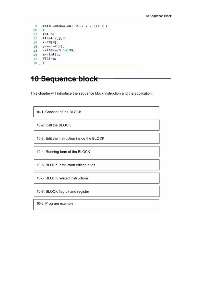
10 Sequence Block
10 Sequence block
This chapter will introduce the sequence block instruction and the application.
10-1. Concept of the BLOCK
10-2. Call the BLOCK
10-3. Edit the instruction inside the BLOCK
10-4. Running form of the BLOCK
10-5. BLOCK instruction editing rules
10-6. BLOCK related instructions
10-7. BLOCK flag bit and register
10-8. Program example

10 Sequence Block
Block instruction:
Instruction
Function Ladder chartChapte
rBlock
SBSTOP Stop the BLOCK SBSTOP S1 S2 10-6-1
SBGOONContinue runningthe BLOCK
SBGOON S1 S2 10-6-1
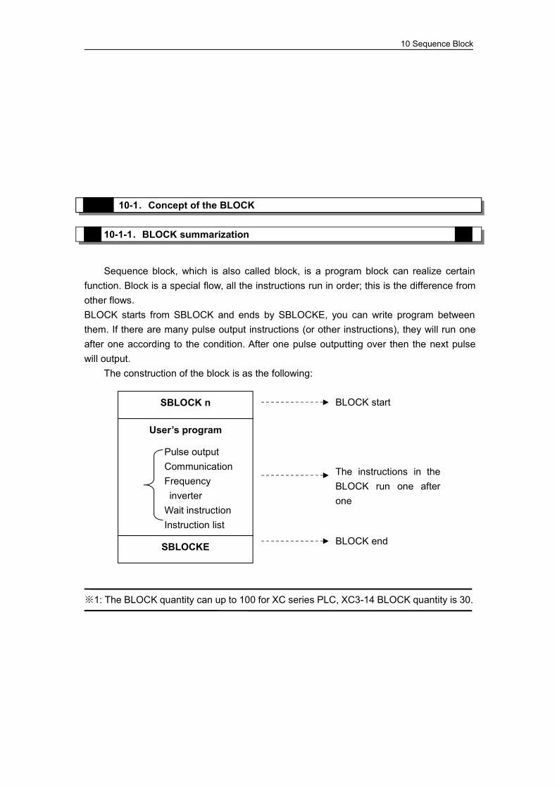
10 Sequence Block
10-1.Concept of the BLOCK
10-1-1.BLOCK summarization
Sequence block, which is also called block, is a program block can realize certainfunction. Block is a special flow, all the instructions run in order; this is the difference fromother flows.BLOCK starts from SBLOCK and ends by SBLOCKE, you can write program betweenthem. If there are many pulse output instructions (or other instructions), they will run oneafter one according to the condition. After one pulse outputting over then the next pulsewill output.
The construction of the block is as the following:
※1: The BLOCK quantity can up to 100 for XC series PLC, XC3-14 BLOCK quantity is 30.
User’s program
Pulse outputCommunicationFrequencyinverterWait instructionInstruction list
SBLOCK n
SBLOCKE
BLOCK start
The instructions in theBLOCK run one afterone
BLOCK end

10 Sequence Block
10-1-2.The reason to use BLOCK
To optimize the editing method of pulse and communication instruction in the processIn former program, XC series PLC can not support many pulse or communicationinstructions in one process, but BLOCK can support this and the instructions will run insequence.
Unavailable (×) Available (√)
Former
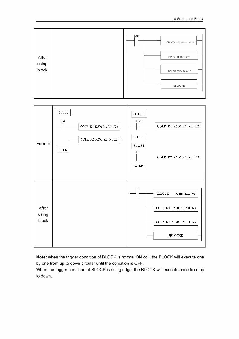
10 Sequence Block
Afterusingblock
DPLSR D0 D2 D4 Y0
M0
DPLSR D6D8D10Y0
SBLOCK Sequence block1
SBLOCKE
Former
Afterusingblock
Note: when the trigger condition of BLOCK is normal ON coil, the BLOCK will execute oneby one from up to down circular until the condition is OFF.When the trigger condition of BLOCK is rising edge, the BLOCK will execute once from upto down.

10 Sequence Block
10-2.Call the BLOCK
In one program file, it can call many BLOCK; the following is the method to addBLOCK in the program.
10-2-1.Add the BLOCK
Open XCPpro software; right click the sequence block in the project bar:
Click “add sequence block” will show below window:
You can edit the program in this window. Upwards and downwards are used tochange the position of the instruction in the block.
There is an “Insert” choice on the bottom left of the window, when selecting it, the addbutton will become insert:
10 Sequence Block
The difference between insert and add:Add is to add instructions in the end of the block; insert can add instruction in any
place in the block.Click add button, you will see the instructions can be added in the block.
For example, add a pulse item in the program:
10 Sequence Block
Click ok, the pulse item is added in the list:
Click ok, the BLOCK will show in the program:
10-2-2.Move the BLOCK
If you want to move the block to other position, you have to select the former blockand delete it.
Then put the cursor in the place you want to move:
10 Sequence Block
Right click the “add to lad” in the project bar:
Now the block is moved to the new place:
10 Sequence Block
10-2-3.Delete the BLOCK
You can select the whole block and delete it. If you want to delete the block forever,please right click the block you want to delete in the project bar and select “deletesequence block”. After this operation, you can not call this block anymore.
10-2-4.Modify the BLOCK
There are two methods to modify the block.(A)double click the start or end instruction to modify all the instructions in the block.

10 Sequence Block
(B)double click one instruction in the block to modify it:
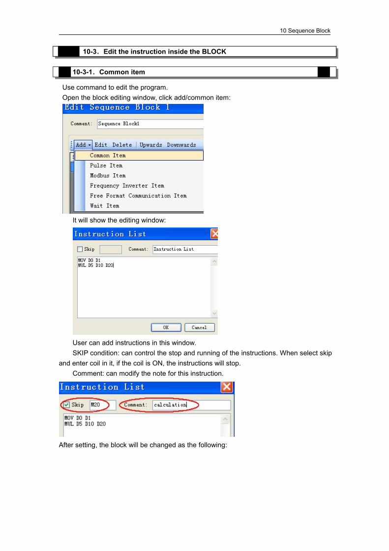
10 Sequence Block
10-3.Edit the instruction inside the BLOCK
10-3-1.Common item
Use command to edit the program.Open the block editing window, click add/common item:
It will show the editing window:
User can add instructions in this window.SKIP condition: can control the stop and running of the instructions. When select skip
and enter coil in it, if the coil is ON, the instructions will stop.Comment: can modify the note for this instruction.
After setting, the block will be changed as the following:
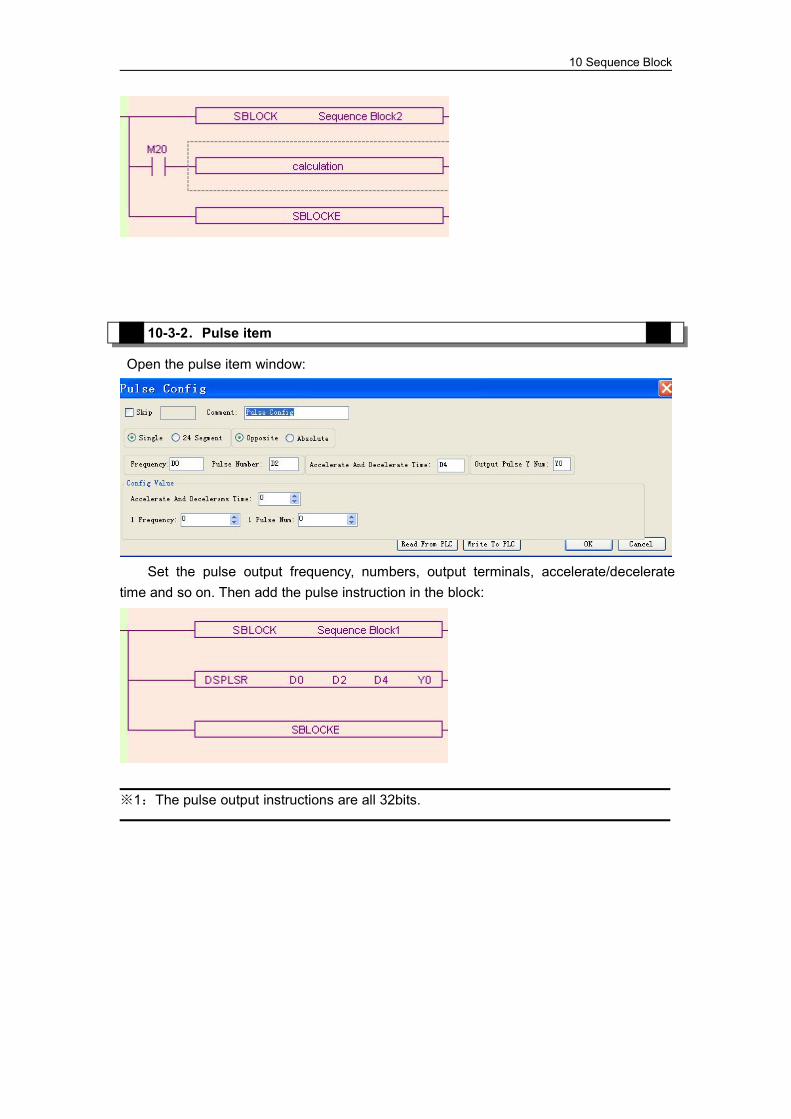
10 Sequence Block
10-3-2.Pulse item
Open the pulse item window:
Set the pulse output frequency, numbers, output terminals, accelerate/deceleratetime and so on. Then add the pulse instruction in the block:
※1:The pulse output instructions are all 32bits.

10 Sequence Block
10-3-3.Modbus item
Open the modbus item window:
Select the modbus instructions, set the address and com port, then software will buildan instruction.
10-3-4.Wait item
There are two modes to wait.(A) flag bit

10 Sequence Block
(B) timer wait
The ladder chart is as the following:
10-3-5.Frequency inverter item
Users only have to set the parameters in below window; the PLC will communicatewith the frequency inverter.
There are four areas in the window, the following will introduce one by one:(A) Inverter station number and serial number
Set the station number of the frequency inverter and the PLC serial port:
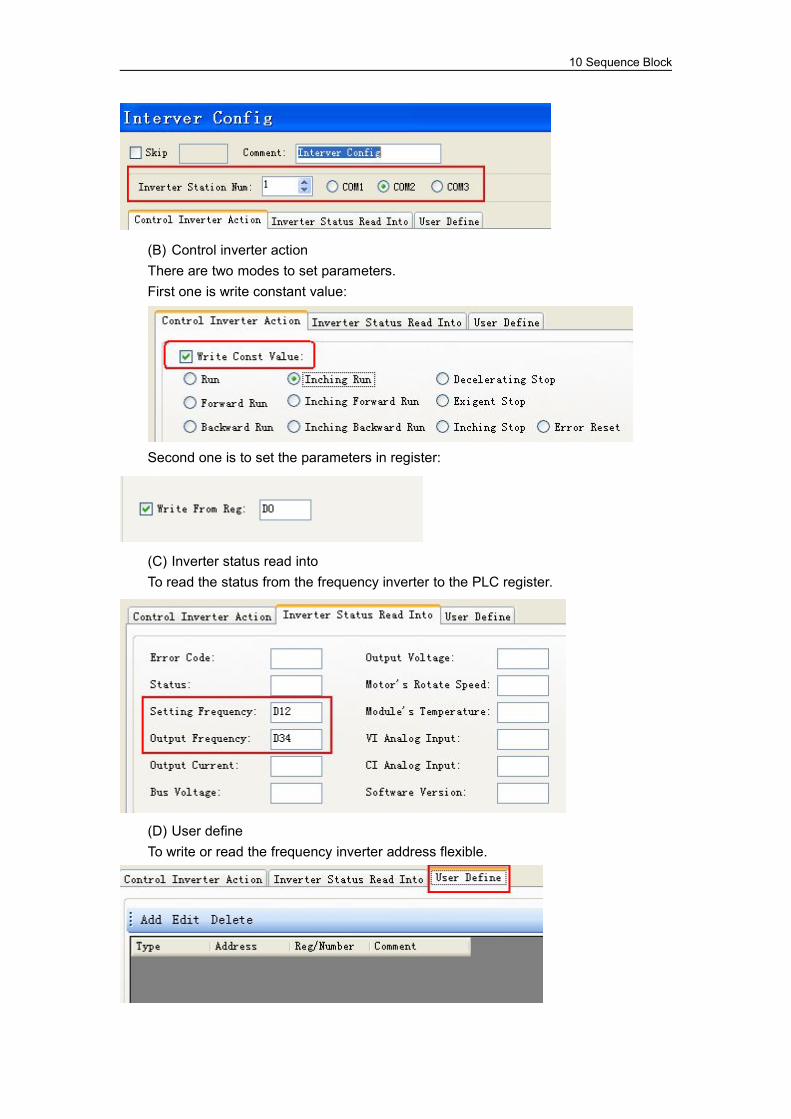
10 Sequence Block
(B) Control inverter actionThere are two modes to set parameters.First one is write constant value:
Second one is to set the parameters in register:
(C) Inverter status read intoTo read the status from the frequency inverter to the PLC register.
(D) User defineTo write or read the frequency inverter address flexible.

10 Sequence Block
For example, add a writing inverter instruction:
Add a reading inverter instruction:
The result after adding:
※1:Frequency inverter instructions will not expand in the block.
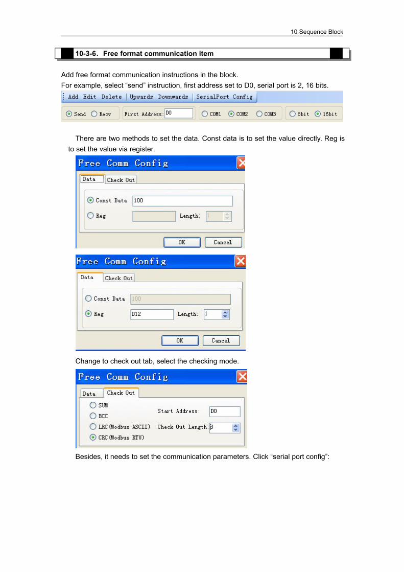
10 Sequence Block
10-3-6.Free format communication item
Add free format communication instructions in the block.For example, select “send” instruction, first address set to D0, serial port is 2, 16 bits.
There are two methods to set the data. Const data is to set the value directly. Reg isto set the value via register.
Change to check out tab, select the checking mode.
Besides, it needs to set the communication parameters. Click “serial port config”:

10 Sequence Block
10-4.Running form of the BLOCK
1. If there are many blocks, they run as the normal program. The block is running whenthe condition is ON.
(A) The condition is normal ON, normal OFF coil
M1SBLOCK Sequence block 1
SBLOCK Sequence block 2
SBLOCK Sequence block 3
M2
M3

10 Sequence Block
Scanning period 1 Scanning period 2 Scanning period 3
Block1 Block1, Block2 Block1, Block2, Block3
M1
M2
M3
(B) The condition is rising or falling edge of pulse
M1
SBLOCK Sequence block 1
SBLOCK Sequence block 2
SBLOCK Sequence block 3
M2
M3
↑
↑
↑
When M1, M2, M3 is from OFF to ON, all these blocks will run once.
2. The instructions in the block run in sequence according to the scanning time. They runone after another when the condition is ON.(A) Without SKIP condition

10 Sequence Block
M2
SBLOCK Sequence block1
Inverter Config
SBLOCKE
↑
M0( )Y0
M1( )Y1
DPLSR D0 D2 D4 Y0
DPLSR D0 D2 D4 Y1
The instructions running sequence in block 1 is shown as below:
Scanning period Scanning period Scanning period Scanning period Scanning period
PLS Y0 PLS Y1 Inverter config
BLOCK running
BLOCK condition is
OFF and all the
sequence
instructions are
M2
(B) With SKIP condition

10 Sequence Block
M2SBLOCK Sequence block1
Inverter config
SBLOCKE
M0( )Y0
M1( )Y1
DPLSR D0 D2 D4 Y0
DPLSR D0 D2 D4 Y1
M3
M4
M5
Explanation:A) When M2 is ON, block 1 is running.B) All the instructions run in sequence in the block.C) M3, M4, M5 are the sign of SKIP, when they are ON, this instruction will not run.D) When M3 is OFF, if no other instructions use this Y0 pulse , DPLSR D0 D2 D4
Y0 will run; if not, the DPLSR D0 D2 D4 Y0 will run after it is released by otherinstructions.
E) After “DPLSR D0 D2 D4 Y0” is over, check M4. If M4 is OFF, check “DPLSR D0D2 D4 Y1”, if M4 is ON, check M5. If M5 is OFF, “inverter config” will run.
10-5.BLOCK instruction editing rules
In the BLOCK, the instruction editing should accord with some standards.
1. Do not use the same pulse output terminal in different BLOCK.
NO(×) YES(√)

10 Sequence Block
DPLSR D0 D2 D4 Y0
M0
SBLOCK Sequence block1
SBLOCKE
M1
M2
DPLSR D10D12D14Y0
SBLOCK Sequence block2
SBLOCKE
DPLSR D0 D2 D4 Y0
M0
SBLOCK Sequence
block1
SBLOCKE
M1
M2
DPLSR D10D12D14Y1
SBLOCK Sequence
block2
SBLOCKE
2. Do not use the same pulse output terminal in BLOCK and main program.
NO(×) YES(√)
DPLSR D0D2D4Y0
M0
M2
DPLSR D10D12D14Y0
SBLOCK Sequence block1
SBLOCKE
DPLSR D0D2D4Y1
M0
M2
DPLSR D10D12D14Y0
SBLOCK Sequence
block1
SBLOCKE
3. There only can be one SKIP condition for one BLOCK instruction.
NO(×) YES(√)
DPLSR D0 D2D4 Y0
M0
SBLOCK Sequence
block1
SBLOCKE
M1 M2
DPLSR D0 D2D4 Y0
M0
SBLOCK Sequence block1
SBLOCKE
M1
4. The SKIP condition only can use M, X, can not use other coil or register.
NO(×) YES(√)
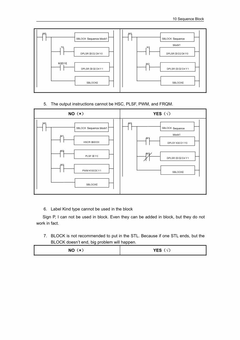
10 Sequence Block
DPLSR D0D2 D4 Y0
M0
SBLOCK Sequence block1
SBLOCKE
T0
M2[D10]
DPLSR D0 D2 D4Y1
DPLSR D0D2 D4 Y0
M0
SBLOCK Sequence
block1
SBLOCKE
X0
M2
DPLSR D0 D2 D4Y1
5. The output instructions cannot be HSC, PLSF, PWM, and FRQM.
NO(×) YES(√)
HSCR C600D0
M0
SBLOCK Sequence block1
SBLOCKE
M1
M2
PLSF D0 Y0
PWM K100D0 Y1
M3
DPLSY K30D1 Y0
M0
SBLOCK Sequence
block1
SBLOCKE
M1
M2
DPLSR D0 D2 D4Y1
6. Label Kind type cannot be used in the block
Sign P, I can not be used in block. Even they can be added in block, but they do notwork in fact.
7. BLOCK is not recommended to put in the STL. Because if one STL ends, but theBLOCK doesn’t end, big problem will happen.
NO(×) YES(√)

10 Sequence Block
10-6.BLOCK related instructions
10-6-1.Instruction explanation
stop running the BLOCK [SBSTOP]
1、SummarizationStop the instructions running in the block[SBSTOP]16 bits SBSTOP 32 bits -Condition NO,NC coil and pulse
edgeSuitabletypes
XC1, XC2, XC3, XC5, XCM,XCC
Hardware Software -
2、OperandOperand Function TypeS1 The number of the BLOCK 16 bits, BINS2 The mode to stop the BLOCK 16 bits, BIN
3、Suitable component
Word Operan
d
Register Consta
nt
Module
D FD ED TD CD DX DY DM DS K/H ID QD
S1 ● ●
S2 K
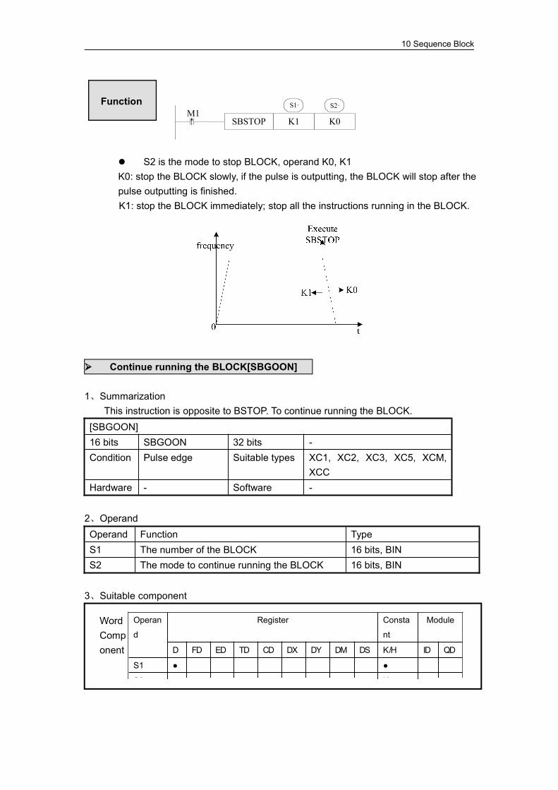
10 Sequence Block
S2 is the mode to stop BLOCK, operand K0, K1K0: stop the BLOCK slowly, if the pulse is outputting, the BLOCK will stop after thepulse outputting is finished.K1: stop the BLOCK immediately; stop all the instructions running in the BLOCK.
Continue running the BLOCK[SBGOON]
1、SummarizationThis instruction is opposite to BSTOP. To continue running the BLOCK.
[SBGOON]16 bits SBGOON 32 bits -Condition Pulse edge Suitable types XC1, XC2, XC3, XC5, XCM,
XCCHardware - Software -
2、OperandOperand Function TypeS1 The number of the BLOCK 16 bits, BINS2 The mode to continue running the BLOCK 16 bits, BIN
3、Suitable component
Function
WordComponent
Operan
d
Register Consta
nt
Module
D FD ED TD CD DX DY DM DS K/H ID QD
S1 ● ●
S2 K
SBSTOP K1 K0M1
S1· S2·
↑
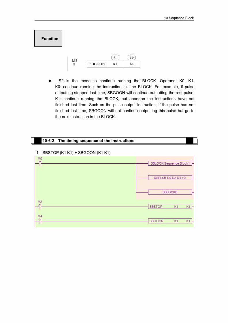
10 Sequence Block
S2 is the mode to continue running the BLOCK. Operand: K0, K1.K0: continue running the instructions in the BLOCK. For example, if pulseoutputting stopped last time, SBGOON will continue outputting the rest pulse.K1: continue running the BLOCK, but abandon the instructions have notfinished last time. Such as the pulse output instruction, if the pulse has notfinished last time, SBGOON will not continue outputting this pulse but go tothe next instruction in the BLOCK.
10-6-2.The timing sequence of the instructions
1. SBSTOP (K1 K1) + SBGOON (K1 K1)
Function
SBGOON K1 K0M3
S1· S2·
↑
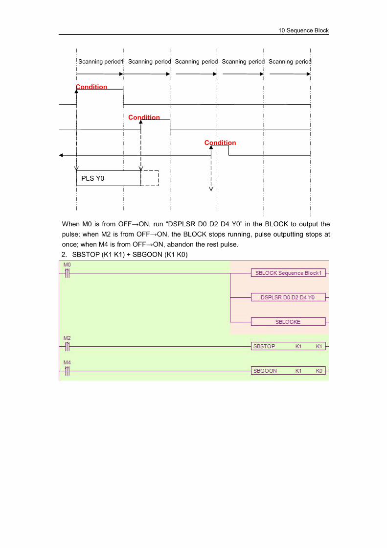
10 Sequence Block
Scanning period1 Scanning period Scanning period
Condition
Scanning period Scanning period
Condition
Condition
PLS Y0
When M0 is from OFF→ON, run “DSPLSR D0 D2 D4 Y0” in the BLOCK to output thepulse; when M2 is from OFF→ON, the BLOCK stops running, pulse outputting stops atonce; when M4 is from OFF→ON, abandon the rest pulse.2. SBSTOP (K1 K1) + SBGOON (K1 K0)
10 Sequence Block
Scanning period 1 Scanning period Scanning period
Condition
Scanning period Scanning period
Condition M2
Condition
PLS Y0
PLS Y0
When M0 is from OFF→ON, run “DSPLSR D0 D2 D4 Y0” in the BLOCK to output thepulse; when M2 is from OFF→ON, the BLOCK stops running, the pulse outputting stopsat once; when M4 is from OFF→ON, output the rest pulses.
3. SBSTOP (K1 K0) + SBGOON (K1 K1)

10 Sequence Block
Scanning period 1 Scanning period Scanning period
Condition
Scanning period Scanning period
Condition M1
Condition
PLS Y0
When M0 is from OFF→ON, run “DSPLSR D0 D2 D4 Y0” in the BLOCK to output thepulse; when M1 is from OFF→ON, stop the BLOCK, the pulse will stop slowly with slope,when M4 is from OFF→ON, abandon the rest pulses.
4. SBSTOP (K1 K0)+ SBGOON (K1 K0)
10 Sequence Block
Scanning period 1 Scanning period Scanning period
Condition M0
Scanning period Scanning period
Condition M1
Condition
PLS Y0
PLS Y0
When M0 is from OFF→ON, run “DSPLSR D0 D2 D4 Y0” in the BLOCK to output thepulse; when M1 is from OFF→ON, stop running the BLOCK, the pulse will stop slowly withslope; when M3 is from OFF→ON, output the rest pulses.
Please note that though the SBSTOP stops the pulse with slope, there maybe stillsome pulses; in this case, if run SBGOON K1 again, it will output the rest of the pulses.
10-7.BLOCK flag bit and register
1、BLOCK flag bit:
Address Function Explanation
M8630
1: running0: not running
M8631 BLOCK1 running flag
M8632 BLOCK2 running flag
……. …….
…….. …….
M8729 BLOCK99 running flag
10 Sequence Block
2、BLOCK flag register
10-8.Program example
Example 1:This example is used in the tracking system. The process is like this:Output some pulses and prohibit the exterior interruption.Continue outputting the pulse but at low speed, and open the exterior interruption. Whenchecked the exterior cursor signal, stop the pulse outputting and machine running.
Ladder chart:
Address Function Explanation
D8630
BLOCK use this value whenmonitoring
D 8631 BLOCK1 current running instruction
D8632 BLOCK2 current running instruction
……. …….
…….. …….
D8729BLOCK99 current runninginstruction
10 Sequence Block
MOV K100 D100
SBLOCKE
MOV K1000 D0
MOV K20000 D2
MOV K0 D4
I0000
IRET
M8000STOP Y0
M8002( )SM8050
X0↑ SBLOCKSequence block1
DPLSR D0 D2 D4 Y0
Instruction list
DPLSR D100 D102 D104 Y0
M8000
MOV K300 D102
MOV K20 D104
( )SM8050
The instruction list content:RST M8050
Notes:M8050: prohibit the exterior interruption
Output the pulses at low speed
PLC power on, prohibit the exterior interruption
BLOCK starts
Output the pulses and move some distance
Reset M8050, open the exterior interruption
BLOCK ends
The first pulse frequency
低速发脉冲The first pulse numbers
低速发脉冲Accelerate/decelerate time for the first pulse
低速发脉冲
The second pulse frequency
低速发脉冲The second pulse numbers
低速发脉冲Accelerate/decelerate time for the second pulse
Stop outputting the pulse
低速发脉冲Close the interruption
低速发脉冲The interruption ends
关闭外部中断
The interruption starts
关闭外部中断
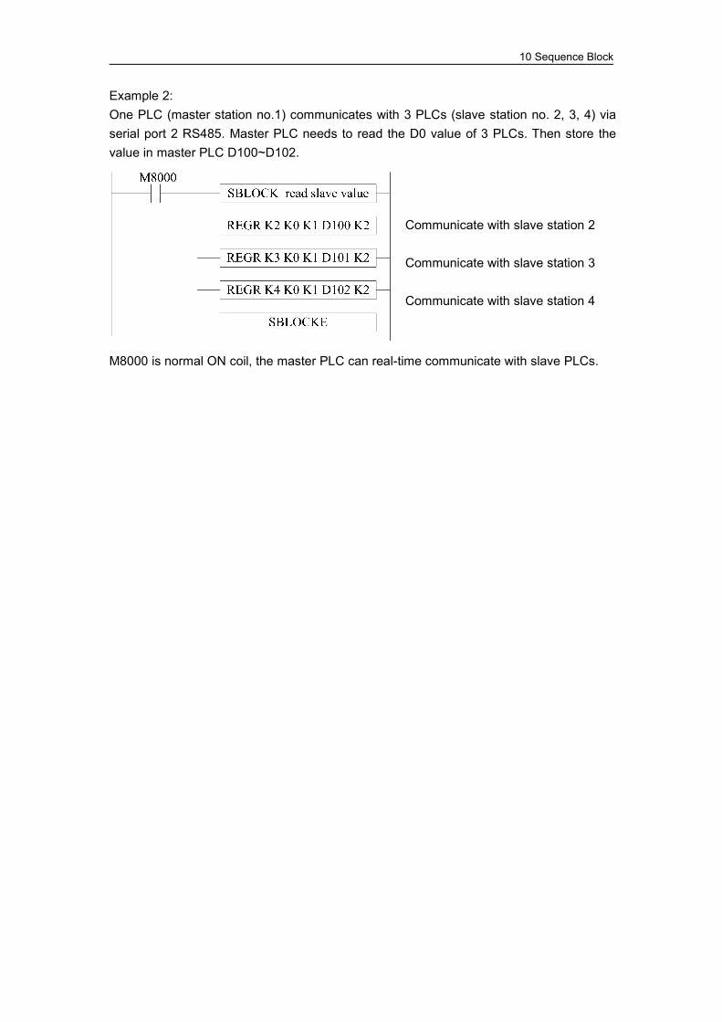
10 Sequence Block
Example 2:One PLC (master station no.1) communicates with 3 PLCs (slave station no. 2, 3, 4) viaserial port 2 RS485. Master PLC needs to read the D0 value of 3 PLCs. Then store thevalue in master PLC D100~D102.
M8000 is normal ON coil, the master PLC can real-time communicate with slave PLCs.
Communicate with slave station 2
Communicate with slave station 3
Communicate with slave station 4
11 Special Function Instructions
11 Special Function Instructions
In this chapter, we mainly introduce PWM pulse width modulation, frequency detect,precise time, interruption etc;
11-1.PWM Pulse Width Modulation
11-2.Frequency Detect
11-3.Precise Time
11-4.Interruption

11 Special Function Instructions
Instructions List
Mnemonic Function Circuit and soft components Chapter
Pulse Width Modulation, Frequency Detection
PWMOutput pulse with thespecified occupiedratio and frequency
PWM S1 S2 D 11-1
FRQM Frequency DetectionFRQM S1 D S2 S3
11-2
Time
STR Precise TimeSTR D1 D2
11-3
STRRRead Precise TimeRegister
STRR S11-3
STRS Stop Precise TimeSTRS S
11-3
Interruption
EI Enable InterruptionEI
11-4-1
DI Disable InterruptionDI
11-4-1
IRET Interruption ReturnIRET
11-4-1
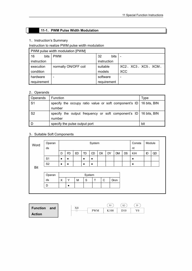
11 Special Function Instructions
11-1.PWM Pulse Width Modulation
1、Instruction’s SummaryInstruction to realize PWM pulse width modulationPWM pulse width modulation [PWM]16 bitsinstruction
PWM 32 bitsinstruction
-
executioncondition
normally ON/OFF coil suitablemodels
XC2、XC3、XC5、XCM、
XCChardwarerequirement
- softwarerequirement
-
2、OperandsOperands Function TypeS1 specify the occupy ratio value or soft component’s ID
number16 bits, BIN
S2 specify the output frequency or soft component’s IDnumber
16 bits, BIN
D specify the pulse output port bit
3、Suitable Soft Components
PWM K100 D10 Y0X0
S1· S2· D·
Operan
ds
System Consta
nt
Module
D FD ED TD CD DX DY DM DS K/H ID QD
S1 ● ● ● ● ●
S2 ● ● ● ● ●
Word
Bit
Operan
ds
System
X Y M S T C Dn.m
D ●
Function and
Action
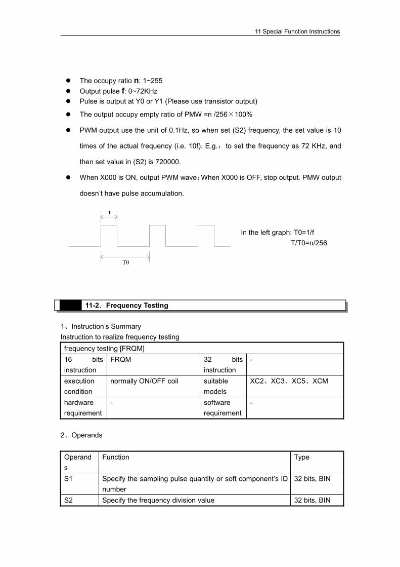
11 Special Function Instructions
T0
t
11-2.Frequency Testing
1、Instruction’s SummaryInstruction to realize frequency testingfrequency testing [FRQM]16 bitsinstruction
FRQM 32 bitsinstruction
-
executioncondition
normally ON/OFF coil suitablemodels
XC2、XC3、XC5、XCM
hardwarerequirement
- softwarerequirement
-
2、Operands
Operands
Function Type
S1 Specify the sampling pulse quantity or soft component’s IDnumber
32 bits, BIN
S2 Specify the frequency division value 32 bits, BIN
The occupy ratio n: 1~255 Output pulse f: 0~72KHz Pulse is output at Y0 or Y1 (Please use transistor output)
The output occupy empty ratio of PMW =n /256×100%
PWM output use the unit of 0.1Hz, so when set (S2) frequency, the set value is 10
times of the actual frequency (i.e. 10f). E.g.:to set the frequency as 72 KHz, and
then set value in (S2) is 720000.
When X000 is ON, output PWM wave;When X000 is OFF, stop output. PMW output
doesn’t have pulse accumulation.
In the left graph: T0=1/fT/T0=n/256
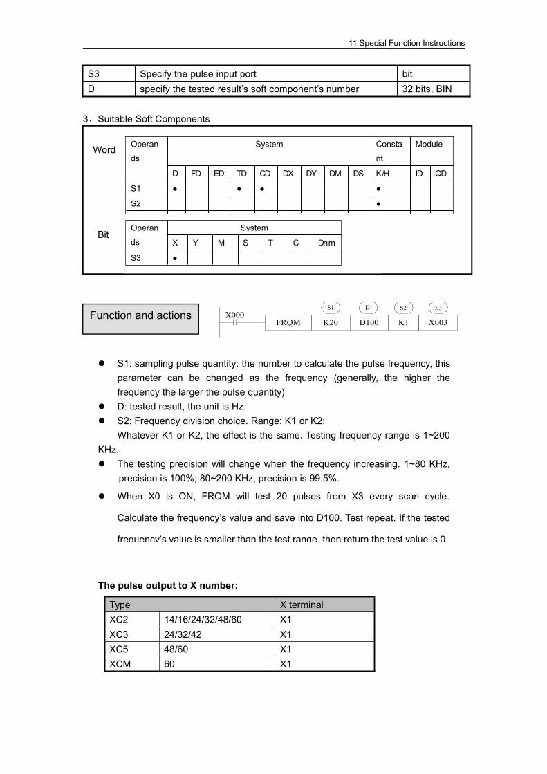
11 Special Function Instructions
S3 Specify the pulse input port bitD specify the tested result’s soft component’s number 32 bits, BIN
3、Suitable Soft Components
FRQM K20 D100 K1 X003X000
D·S1· S2· S3·
Operan
ds
System Consta
nt
Module
D FD ED TD CD DX DY DM DS K/H ID QD
S1 ● ● ● ●
S2 ●
D ● ● ●
Word
BitOperan
ds
System
X Y M S T C Dn.m
S3 ●
Function and actions
S1: sampling pulse quantity: the number to calculate the pulse frequency, thisparameter can be changed as the frequency (generally, the higher thefrequency the larger the pulse quantity)
D: tested result, the unit is Hz. S2: Frequency division choice. Range: K1 or K2;
Whatever K1 or K2, the effect is the same. Testing frequency range is 1~200KHz. The testing precision will change when the frequency increasing. 1~80 KHz,
precision is 100%; 80~200 KHz, precision is 99.5%.
When X0 is ON, FRQM will test 20 pulses from X3 every scan cycle.
Calculate the frequency’s value and save into D100. Test repeat. If the tested
frequency’s value is smaller than the test range, then return the test value is 0.
The pulse output to X number:
Type X terminalXC2 14/16/24/32/48/60 X1XC3 24/32/42 X1XC5 48/60 X1XCM 60 X1

11 Special Function Instructions
11-3.Precise Time
1、Instruction ListRead and stop precise time when execute precise time;precise time [STR]16 bitsinstruction
- 32 bitsinstruction
STR
executioncondition
edge activation suitablemodels
XC2、XC3、XC5、XCM、XCC
hardwarerequirement
- softwarerequirements
-
read precise time [STRR]16 bitsinstruction
- 32 bitsinstruction
STRR
executioncondition
edge activation suitablemodels
XC2、XC3、XC5、XCM、XCC
hardwarerequirement
V3.0e and above softwarerequirements
-
stop precise time [STRS]16 bitsinstruction
- 32 bitsinstruction
STRS
executioncondition
edge activation suitablemodels
XC2、XC3、XC5、XCM、XCC
hardwarerequirement
V3.0e and above softwarerequirements
-
2、OperandsOperands
Function Type
D Timer Number bitD1 Timer Number bitD2 specify timer’s value or soft component’s ID
number16 bits, BIN
3、Suitable Soft Components
operan
ds
system consta
nt
module
D FD ED TD CD DX DY DM DS K/H ID QD
D2 ● ● ● ● ●
Word

11 Special Function Instructions
《Precise Time》
STR T600 K100X0
D1· D2·
Y0T600
RST T600M0
X0
T600
100ms 100ms
M0
《read the precise time》、《stop precise time》
Bitoperan
ds
system
X Y M S T C Dn.m
D ●
D1 ●
Function andaction
D1: Timer’s number. Range: T600~T618 (T600、 T602、 T604… T618, thenumber should be even)
D2: Time Value
The precise timer works in form of 1ms The precise timer is 32 bits, the count range is 0~+2,147,483,647. When executing STR, the timer will be reset before start timing. When X0 turns from OFF to ON, timer T600 starts to time, when time
accumulation reaches 100ms, set T600; if X0 again turns from OFF to ON,timer T600 turns from ON to OFF,restart to time, when time accumulationreaches 100ms, T600 reset again. See graph below:
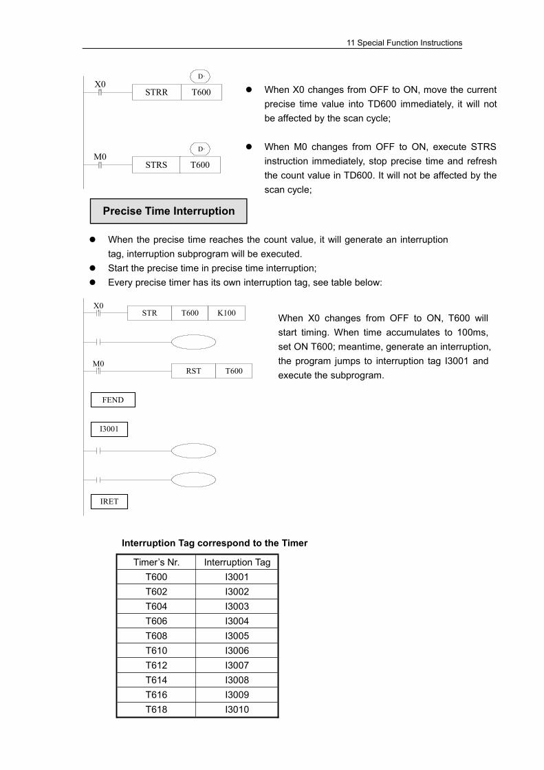
11 Special Function Instructions
STRR T600X0
STRS T600M0
D·
D·
STR T600 K100X0
RST T600M0
I3001
IRET
FEND
Interruption Tag correspond to the Timer
Timer’s Nr. Interruption TagT600 I3001T602 I3002T604 I3003T606 I3004T608 I3005T610 I3006T612 I3007T614 I3008T616 I3009T618 I3010
When the precise time reaches the count value, it will generate an interruptiontag, interruption subprogram will be executed.
Start the precise time in precise time interruption; Every precise timer has its own interruption tag, see table below:
Precise Time Interruption
When X0 changes from OFF to ON, T600 willstart timing. When time accumulates to 100ms,set ON T600; meantime, generate an interruption,the program jumps to interruption tag I3001 andexecute the subprogram.
When X0 changes from OFF to ON, move the currentprecise time value into TD600 immediately, it will notbe affected by the scan cycle;
When M0 changes from OFF to ON, execute STRSinstruction immediately, stop precise time and refreshthe count value in TD600. It will not be affected by thescan cycle;
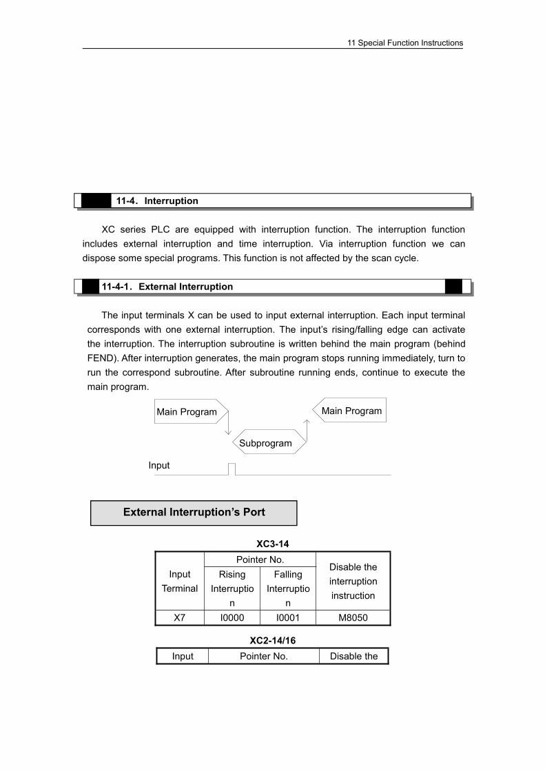
11 Special Function Instructions
11-4.Interruption
XC series PLC are equipped with interruption function. The interruption functionincludes external interruption and time interruption. Via interruption function we candispose some special programs. This function is not affected by the scan cycle.
11-4-1.External Interruption
The input terminals X can be used to input external interruption. Each input terminalcorresponds with one external interruption. The input’s rising/falling edge can activatethe interruption. The interruption subroutine is written behind the main program (behindFEND). After interruption generates, the main program stops running immediately, turn torun the correspond subroutine. After subroutine running ends, continue to execute themain program.
XC3-14
InputTerminal
Pointer No.Disable theinterruptioninstruction
RisingInterruptio
n
FallingInterruptio
nX7 I0000 I0001 M8050
XC2-14/16Input Pointer No. Disable the
Main Program Main Program
Subprogram
Input
External Interruption’s PortDefinition
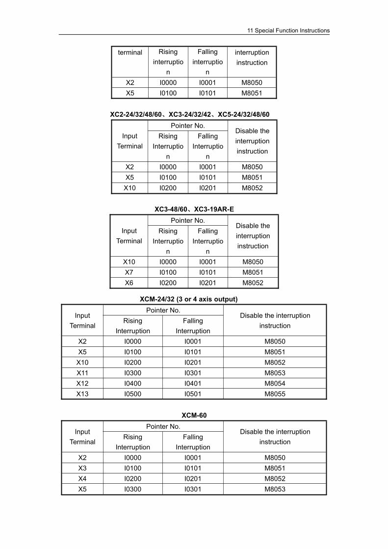
11 Special Function Instructions
terminal interruptioninstruction
Risinginterruptio
n
Fallinginterruptio
nX2 I0000 I0001 M8050X5 I0100 I0101 M8051
XC2-24/32/48/60、XC3-24/32/42、XC5-24/32/48/60
InputTerminal
Pointer No.Disable theinterruptioninstruction
RisingInterruptio
n
FallingInterruptio
nX2 I0000 I0001 M8050X5 I0100 I0101 M8051X10 I0200 I0201 M8052
XC3-48/60、XC3-19AR-E
InputTerminal
Pointer No.Disable theinterruptioninstruction
RisingInterruptio
n
FallingInterruptio
nX10 I0000 I0001 M8050X7 I0100 I0101 M8051X6 I0200 I0201 M8052
XCM-24/32 (3 or 4 axis output)
InputTerminal
Pointer No.Disable the interruption
instructionRising
InterruptionFalling
InterruptionX2 I0000 I0001 M8050X5 I0100 I0101 M8051X10 I0200 I0201 M8052X11 I0300 I0301 M8053X12 I0400 I0401 M8054X13 I0500 I0501 M8055
XCM-60
InputTerminal
Pointer No.Disable the interruption
instructionRising
InterruptionFalling
InterruptionX2 I0000 I0001 M8050X3 I0100 I0101 M8051X4 I0200 I0201 M8052X5 I0300 I0301 M8053

11 Special Function Instructions
XCC-24
InputTerminal
Pointer No.Disable the interruption
instructionRising
InterruptionFalling
InterruptionX14 I0000 I0001 M8050X15 I0100 I0101 M8051
XCC-32
InputTerminal
Pointer No.Disable the interruption
instructionRising
InterruptionFalling
InterruptionX14 I0000 I0001 M8050X15 I0100 I0101 M8051X16 I0200 I0201 M8052X17 I0300 I0301 M8053
Enable Interruption [EI]、Disable Interruption [DI]、Interruption Return [IRET]
If use EI instruction to allowinterruption, then when scanning theprogram, if interruption input changesfrom OFF to be ON, then executesubroutine① 、 ②, return to theoriginal main program;
Interruption pointer (I****) should bebehind FEND instruction;
PLC is default to allow interruption
Interruption Instruction
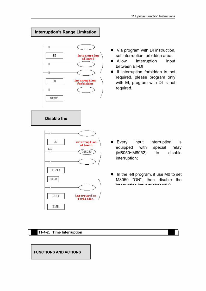
11 Special Function Instructions
11-4-2.Time Interruption
Via program with DI instruction,set interruption forbidden area;
Allow interruption inputbetween EI~DI
If interruption forbidden is notrequired, please program onlywith EI, program with DI is notrequired.
Every input interruption isequipped with special relay(M8050~M8052) to disableinterruption;
In the left program, if use M0 to setM8050 “ON”, then disable theinterruption input at channel 0.
FUNCTIONS AND ACTIONS
Interruption’s Range Limitation
Disable the
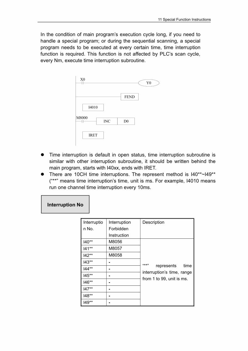
11 Special Function Instructions
Y0
FEND
I4010
INC D0
IRET
X0
M8000
Interruption No.
InterruptionForbiddenInstruction
Description
I40** M8056
“**” represents timeinterruption’s time, rangefrom 1 to 99, unit is ms.
I41** M8057I42** M8058I43** -I44** -I45** -I46** -I47** -I48** -I49** -
In the condition of main program’s execution cycle long, if you need tohandle a special program; or during the sequential scanning, a specialprogram needs to be executed at every certain time, time interruptionfunction is required. This function is not affected by PLC’s scan cycle,every Nm, execute time interruption subroutine.
Time interruption is default in open status, time interruption subroutine issimilar with other interruption subroutine, it should be written behind themain program, starts with I40xx, ends with IRET.
There are 10CH time interruptions. The represent method is I40**~I49**(“**” means time interruption’s time, unit is ms. For example, I4010 meansrun one channel time interruption every 10ms.
Interruption No
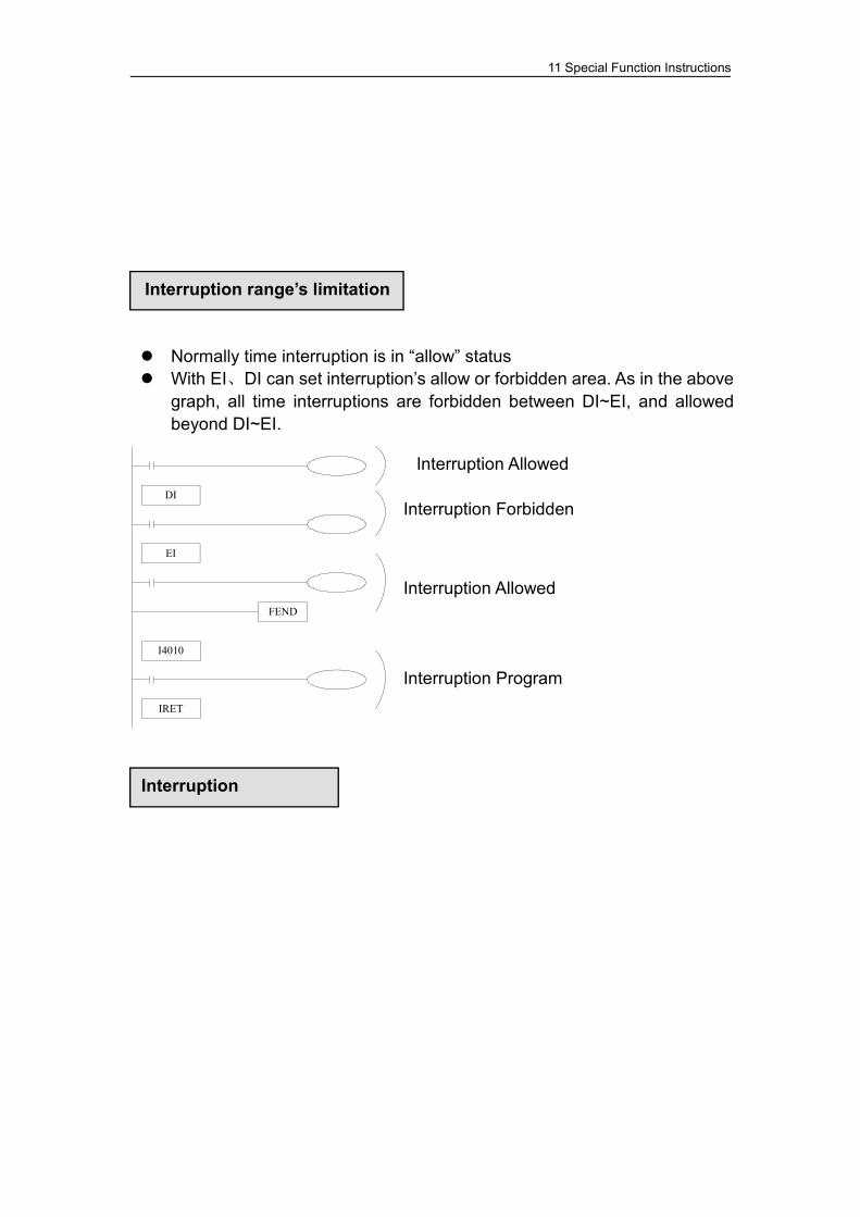
11 Special Function Instructions
FEND
I4010
IRET
DI
EI
Normally time interruption is in “allow” status With EI、DI can set interruption’s allow or forbidden area. As in the above
graph, all time interruptions are forbidden between DI~EI, and allowedbeyond DI~EI.
Interruption Allowed
Interruption Allowed
Interruption Forbidden
Interruption Program
Interruption range’s limitation
InterruptionForbidden
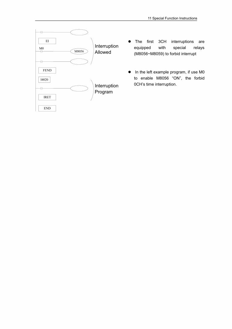
11 Special Function Instructions
EI
M8056
FEND
I4020
IRET
END
M0
The first 3CH interruptions areequipped with special relays(M8056~M8059) to forbid interrupt
In the left example program, if use M0to enable M8056 “ON”, the forbid0CH’s time interruption.
InterruptionAllowed
InterruptionProgram

12 Application Program Samples
In this chapter, we make some samples about pulse output instruction, Modbuscommunication instructions and free format communication instructions etc.
12-1.Pulse Output Sample
12-2.Modbus Communication Sample
12-3.Free Format Communication Sample

12-1.Pulse Output Application
Example: send high frequency and low frequency of pulseParameters:Stepping motor parameters: step angle= 1.8 degrees/step, scale=40, pulse number perrotate is 8000High frequency pulse: maximum frequency is 100 KHz, total pulse number is 24000 (3rotate)Low frequency pulse: maximum frequency is 10 KHz, total pulse number is 8000 (1rotates)
Ladder Program:
Explanation:When PLC changes from STOP to RUN, set ON M0, set the high frequency parameter D0,D2, low frequency parameter D4, D6, speed up/down time D20, clear D8~D11, set ON M1,set OFF M0. The motor rotates at high frequency for 3 turns, set ON M8170; then themotor rotates at low frequency for 1 turn, set OFF M8170, set OFF M1.
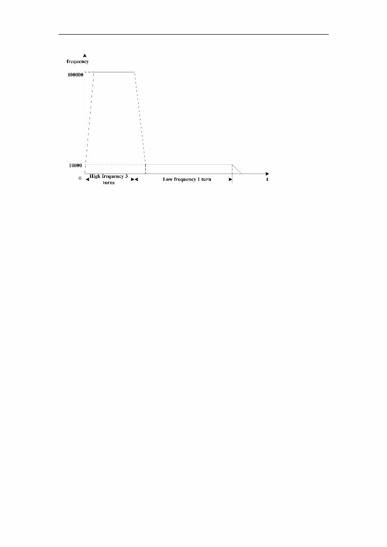
12-2.MODBUS COMMUNICATION SAMPLES
Example 1: one master station communicates with 3 slave stations.
Operation:(1) Write content in D10~D14 to D10~D14 of slave station 2;(2) Read D15~D19 of the slave station 2 to D15~D19 of the mater station; anyhow, writethe first five registers’ content to the slaves, the left five registers are used to store thecontent from the slaves;(3) Slave station 3 and 4 are similar;Soft component’s comments:D0: communication station numberD1: offsetM2: station 2 communication errorM3: station 3 communication errorM4: station 4 communication errorM8137: COM2 communication error endsignalM8138: COM2 communication correct endsignal
Ladder chart
S0: write the target stationS1: read the target stationS2: judge the communication statusS3: offset the communication addressT200: communication interval 1T201: communication interval 2D20: plus one for write error timesD21: plus one for read error times


Program Explanation:When PLC turns from STOP to RUN, M8002 gets a scan cycle. S0 flow open, write themaster’s D10~D14 to slave 2 D10~D14. If the communication is successful, it goes to thenext flow; if not, it will try three times then go to the S1 flow. It delays for a while then readD15~D19 of station 2. The method is similar to S0 flow. Then go to S2 flow. If thecommunication is failed, set ON M23. Then it goes to S3 flow. S3 flow will judge thestation no, if the no. is less than 4, the station no. will plus 1, offset value plus 10; if not, thestation no. will start again from 2.
Example 2: Spectra PLC writes frequency to two inverters via Modbus.
Set the first inverter’s station no. to 1; set the second inverter’s station no. to 2; store thefrequency in D1000 and D2000. Communicate with inverter via serial port.
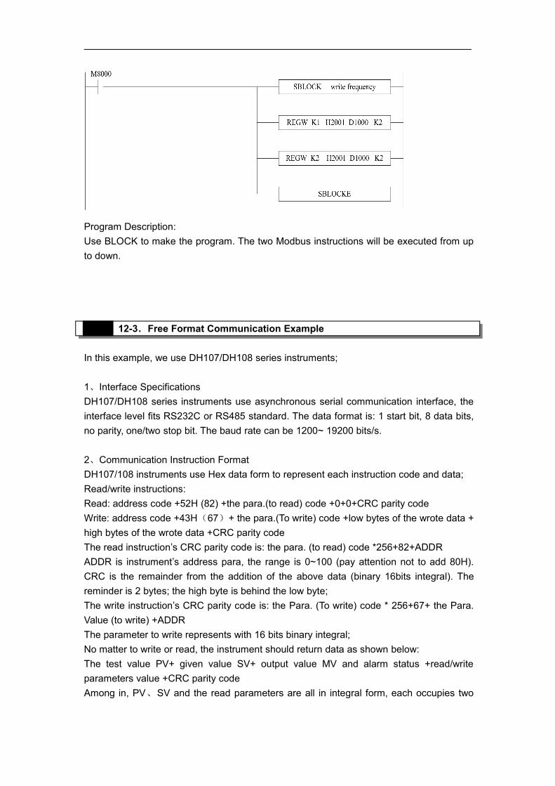
Program Description:Use BLOCK to make the program. The two Modbus instructions will be executed from upto down.
12-3.Free Format Communication Example
In this example, we use DH107/DH108 series instruments;
1、Interface SpecificationsDH107/DH108 series instruments use asynchronous serial communication interface, theinterface level fits RS232C or RS485 standard. The data format is: 1 start bit, 8 data bits,no parity, one/two stop bit. The baud rate can be 1200~ 19200 bits/s.
2、Communication Instruction FormatDH107/108 instruments use Hex data form to represent each instruction code and data;Read/write instructions:Read: address code +52H (82) +the para.(to read) code +0+0+CRC parity codeWrite: address code +43H(67)+ the para.(To write) code +low bytes of the wrote data +high bytes of the wrote data +CRC parity codeThe read instruction’s CRC parity code is: the para. (to read) code *256+82+ADDRADDR is instrument’s address para, the range is 0~100 (pay attention not to add 80H).CRC is the remainder from the addition of the above data (binary 16bits integral). Thereminder is 2 bytes; the high byte is behind the low byte;The write instruction’s CRC parity code is: the Para. (To write) code * 256+67+ the Para.Value (to write) +ADDRThe parameter to write represents with 16 bits binary integral;No matter to write or read, the instrument should return data as shown below:The test value PV+ given value SV+ output value MV and alarm status +read/writeparameters value +CRC parity codeAmong in, PV、SV and the read parameters are all in integral form, each occupies two

bytes, MV occupies one byte, the value range is 0~220, alarm status occupies one byte,CRC parity code occupies two bytes, totally 10 byes.CRC parity code is the reminder from the result of PV+SV+ (alarm status *256+MV) +Para. Value +ADDR;(For details, please refer to AIBUS communication description)
3、Write the programAfter power on the PLC, the PLC read the current temperature every 40ms. During thisperiod, the user can write the set temperature.Data zone definition: buffer area of sending data D10~D19
Buffer area of accepting data D20~D29Instruction’s station number: D30Read command’s value: D31=52 HWrite command’s value: D32=43 HParameter’s code: D33Temperature setting: D34CRC parity code: D36Temperature display: D200, D201
The send data form: 81H 43H 00H c8H 00H 0cH 01H (current temperature display)Communication parameters setting: baud rate: 9600, 8 data bits, 2 stop bits, no paritySet FD8220=255; FD8221=5(The hardware and software must be V2.4 or above)
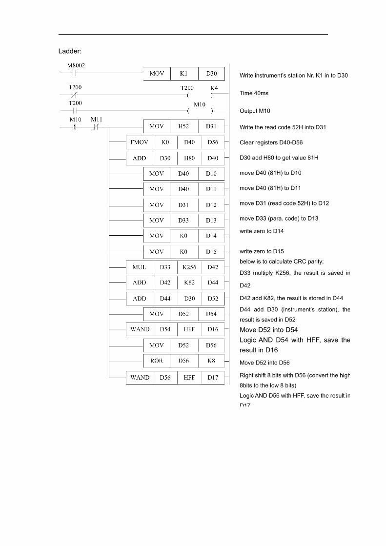
Ladder:
Write instrument’s station Nr. K1 in to D30
Time 40ms
Output M10
Write the read code 52H into D31
Clear registers D40-D56
D30 add H80 to get value 81H
move D40 (81H) to D10
move D40 (81H) to D11
move D31 (read code 52H) to D12
move D33 (para. code) to D13
write zero to D14
write zero to D15
below is to calculate CRC parity;
D33 multiply K256, the result is saved in
D42
D42 add K82, the result is stored in D44
D44 add D30 (instrument’s station), the
result is saved in D52
Move D52 into D54Logic AND D54 with HFF, save theresult in D16
Move D52 into D56
Right shift 8 bits with D56 (convert the high
8bits to the low 8 bits)
Logic AND D56 with HFF, save the result in
D17
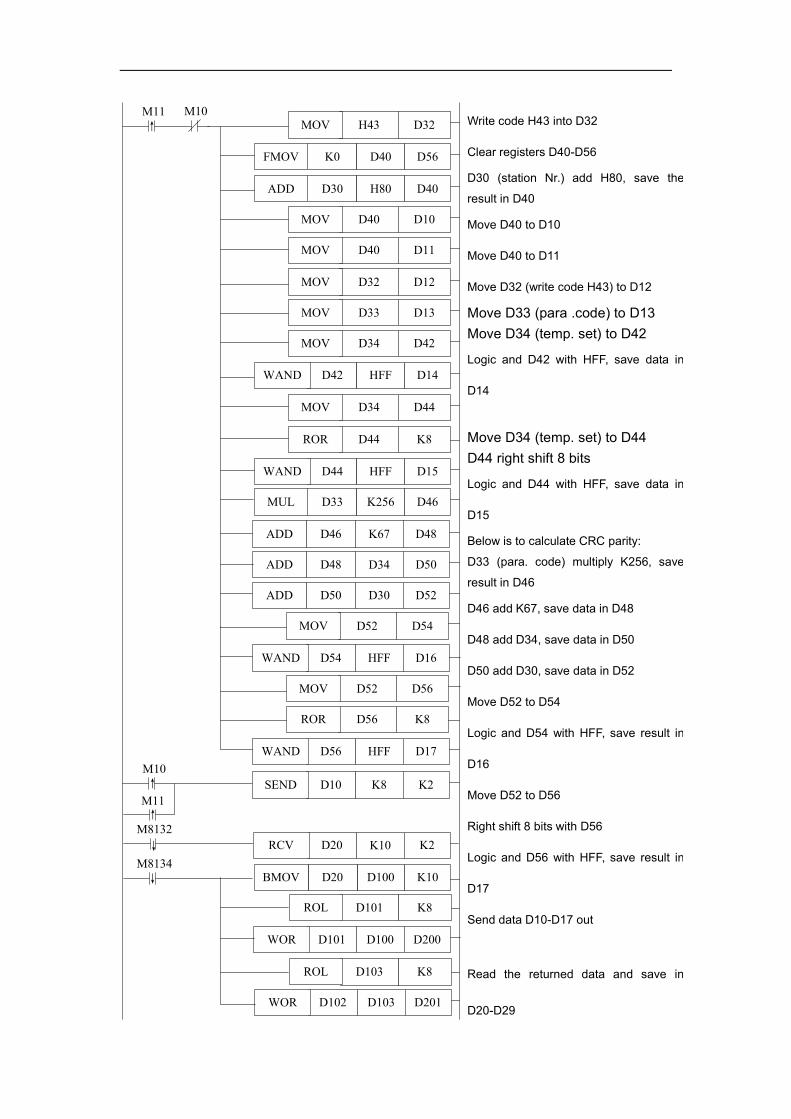
↓
M11↑
M10H43 D32MOV
K0 D40FMOV D56
D30 H80ADD D40
D40 D10MOV
D40 D11MOV
D32 D12MOV
D33 D13MOV
D34 D42MOV
D34 D44MOV
D33 K256MUL D46
D46 K67ADD D48
D48 D34ADD D50
D52 D54MOV
D44 HFFWAND D15
D52 D56MOV
D44 K8ROR
D54 HFFWAND D16
D42 HFFWAND D14
D50 D30ADD D52
D56 K8ROR
D56 HFFWAND D17M10↑ D10 K8SEND K2
M11↑
M8132D20 K10RCV K2
D101 K8ROL
D101 D100WOR D200
D103 K8ROL
D102 D103WOR D201
M8134D100 K10D20BMOV↓
Write code H43 into D32
Clear registers D40-D56
D30 (station Nr.) add H80, save the
result in D40
Move D40 to D10
Move D40 to D11
Move D32 (write code H43) to D12
Move D33 (para .code) to D13Move D34 (temp. set) to D42
Logic and D42 with HFF, save data in
D14
Move D34 (temp. set) to D44D44 right shift 8 bits
Logic and D44 with HFF, save data in
D15
Below is to calculate CRC parity:
D33 (para. code) multiply K256, save
result in D46
D46 add K67, save data in D48
D48 add D34, save data in D50
D50 add D30, save data in D52
Move D52 to D54
Logic and D54 with HFF, save result in
D16
Move D52 to D56
Right shift 8 bits with D56
Logic and D56 with HFF, save result in
D17
Send data D10-D17 out
Read the returned data and save in
D20-D29
Move the returned data to D100~109
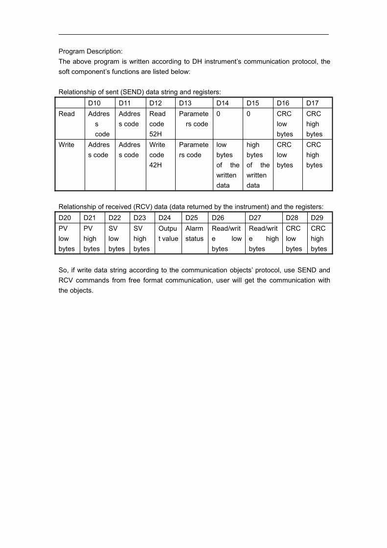
Program Description:The above program is written according to DH instrument’s communication protocol, thesoft component’s functions are listed below:
Relationship of sent (SEND) data string and registers:D10 D11 D12 D13 D14 D15 D16 D17
Read Addresscode
Address code
Readcode52H
Parameters code
0 0 CRClowbytes
CRChighbytes
Write Address code
Address code
Writecode42H
Parameters code
lowbytesof thewrittendata
highbytesof thewrittendata
CRClowbytes
CRChighbytes
Relationship of received (RCV) data (data returned by the instrument) and the registers:D20 D21 D22 D23 D24 D25 D26 D27 D28 D29PVlowbytes
PVhighbytes
SVlowbytes
SVhighbytes
Output value
Alarmstatus
Read/write lowbytes
Read/write highbytes
CRClowbytes
CRChighbytes
So, if write data string according to the communication objects’ protocol, use SEND andRCV commands from free format communication, user will get the communication withthe objects.
Appendix special soft device list
Appendix 1 Special soft device list
Here we mainly introduce the functions of special soft device, data register and FlashROM,and introduce the address of expansion. Users can scan fast.
Appendix 1-1.Special Auxiliary Relay List
Appendix 1-2.Special Data Register List
Appendix 1-3.Special Module Address List
Appendix 1-4.Special Flash Register List

Appendix special soft device list
Appendix 1-1.Special Auxiliary Relay List
ID Function Description
M8000Normally ON coilwhen running
M8000 keeps being ONstatus when PLC is
running
M8001Normally OFF coilwhen running
M8001 keeps being OFFstatus when PLC isrunning
M8002Initial positivepulse coil
M8002 be ON in firstscan cycle
M8003Initial negativepulse coil
M8003 be OFF in firstscan cycle
ID Function Description
M8011Shake with the cycle of10ms
5ms
5ms
M8012Shake with the cycle of100ms
50ms
50ms
M8013Shake with the cycle of10sec
0.5s
0.5s
M8014Shake with the cycle of1min
30s
30s
PC Status (M8000-M8003)
Clock (M8011-M8014)
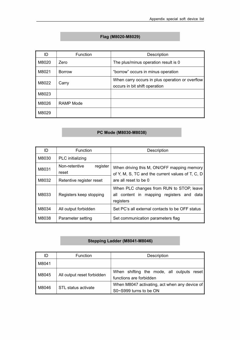
Appendix special soft device list
ID Function Description
M8020 Zero The plus/minus operation result is 0
M8021 Borrow “borrow” occurs in minus operation
M8022 CarryWhen carry occurs in plus operation or overflowoccurs in bit shift operation
M8023
M8026 RAMP Mode
M8029
ID Function Description
M8030 PLC initializing
M8031Non-retentive registerreset
When driving this M, ON/OFF mapping memoryof Y, M, S, TC and the current values of T, C, Dare all reset to be 0M8032 Retentive register reset
M8033 Registers keep stoppingWhen PLC changes from RUN to STOP, leaveall content in mapping registers and dataregisters
M8034 All output forbidden Set PC’s all external contacts to be OFF status
M8038 Parameter setting Set communication parameters flag
ID Function Description
M8041
M8045 All output reset forbiddenWhen shifting the mode, all outputs resetfunctions are forbidden
M8046 STL status activateWhen M8047 activating, act when any device ofS0~S999 turns to be ON
Flag (M8020-M8029)
PC Mode (M8030-M8038)
Stepping Ladder (M8041-M8046)

Appendix special soft device list
ID Function DescriptionM8050I000□ Forbid the input interruption 0
After executing EI instruction, even theinterruption is allowed, but if M acts at thistime, the correspond input interruptioncouldn’t act separatelyE.g.:when M8050 is ON, interrupt I000□is forbidden
M8051I010□ Forbid the input interruption 1M8052I020□ Forbid the input interruption 2M8053I030□ Forbid the input interruption 3M8054I040□ Forbid the input interruption 4M8055I050□ Forbid the input interruption 5M8056I40□□ Forbid the time interruption 0 After executing EI instruction, even the
interruption is allowed, but if M acts at thistime, the correspond time interruptioncouldn’t act separately
M8057I41□□ Forbid the time interruption 1M8058I42□□ Forbid the time interruption 2
M8059 Forbid the interruption Forbid all interruption
ID Function Description
M8067 Operation error happen when calculating
M8070 Scan time out
M8071 No user program Internal codes parity error
M8072 User program error execution codes or configure table parity error
Interruption (M8050-M8059)
Error Testing (M8067-M8072)

Appendix special soft device list
COM1
ID Function DescriptionM8120M8121 Waiting to send via RS232M8122 “sending by RS232” flagM8123 “RS232 receiving finish” flagM8124 RS232 receiving flag
M8125 “Receive incomplete” flagacceptance ends normally, but theaccepted data number is less than therequired number
M8126 Global signalM8127 “Accept error” flagM8128 “ Accept correct” flagM8129
COM2
M8130M8131 Waiting to send via RS232M8132 “sending by RS232” flagM8133 “RS232 receiving finish” flagM8134 RS232 receiving flag
M8135 “Receive incomplete” flagacceptance ends normally, but theaccepted data number is less than therequired number
M8136 Global signalM8137 “Accept error” flagM8138 “ Accept correct” flagM8139
COM3
M8140M8141 Waiting to send via RS232M8142 “sending by RS232” flagM8143 “RS232 receiving finish” flagM8144 RS232 receiving flag
M8145 “Receive incomplete” flagacceptance ends normally, but theaccepted data number is less than therequired number
M8146 Global signalM8147 “Accept error” flagM8148 “ Accept correct” flagM8149
Communication (M8120-M8148)
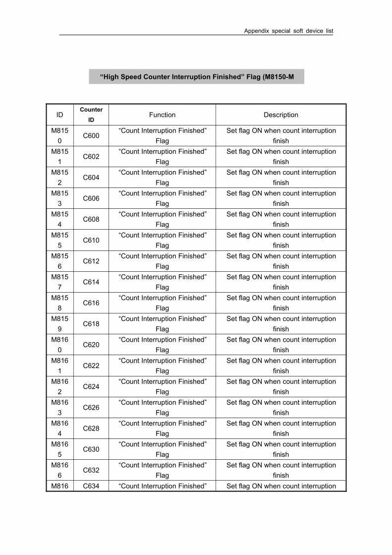
Appendix special soft device list
IDCounterID
Function Description
M8150
C600“Count Interruption Finished”
FlagSet flag ON when count interruption
finishM8151
C602“Count Interruption Finished”
FlagSet flag ON when count interruption
finishM8152
C604“Count Interruption Finished”
FlagSet flag ON when count interruption
finishM8153
C606“Count Interruption Finished”
FlagSet flag ON when count interruption
finishM8154
C608“Count Interruption Finished”
FlagSet flag ON when count interruption
finishM8155
C610“Count Interruption Finished”
FlagSet flag ON when count interruption
finishM8156
C612“Count Interruption Finished”
FlagSet flag ON when count interruption
finishM8157
C614“Count Interruption Finished”
FlagSet flag ON when count interruption
finishM8158
C616“Count Interruption Finished”
FlagSet flag ON when count interruption
finishM8159
C618“Count Interruption Finished”
FlagSet flag ON when count interruption
finishM8160
C620“Count Interruption Finished”
FlagSet flag ON when count interruption
finishM8161
C622“Count Interruption Finished”
FlagSet flag ON when count interruption
finishM8162
C624“Count Interruption Finished”
FlagSet flag ON when count interruption
finishM8163
C626“Count Interruption Finished”
FlagSet flag ON when count interruption
finishM8164
C628“Count Interruption Finished”
FlagSet flag ON when count interruption
finishM8165
C630“Count Interruption Finished”
FlagSet flag ON when count interruption
finishM8166
C632“Count Interruption Finished”
FlagSet flag ON when count interruption
finishM816 C634 “Count Interruption Finished” Set flag ON when count interruption
“High Speed Counter Interruption Finished” Flag (M8150-M

Appendix special soft device list
Absolute, relative bit:
7 Flag finishM8168
C636“Count Interruption Finished”
FlagSet flag ON when count interruption
finishM8169
C638“Count Interruption Finished”
FlagSet flag ON when count interruption
finish
ID Pulse ID Function specificationM8170
PULSE_1
“sending pulse” flag Being ON when sending the pulse,
M8171
overflow flag of “32 bits pulsesending”
When overflow, Flag is on
M8172
Direction flag1 is positive direction, thecorrespond direction port is on
M8173
PULSE_2
“sending pulse” flag Being ON when sending the pulse,
M8174
overflow flag of “32 bits pulsesending”
When overflow, Flag is on
M8175
Direction flag1 is positive direction, thecorrespond direction port is on
M8176
PULSE_3
“sending pulse” flag Being ON when sending the pulse,
M8177
overflow flag of “32 bits pulsesending”
When overflow, Flag is on
M8178
Direction flag1 is positive direction, thecorrespond direction port is on
M8179
PULSE_4
“sending pulse” flag Being ON when sending the pulse,
M8180
overflow flag of “32 bits pulsesending”
When overflow, Flag is on
M8181
Direction flag1 is positive direction, thecorrespond direction port is on
ID function specificationM8190 C600 (24 segments) 1 is absolute, 0 is relativeM8191 C602 (24 segments) 1 is absolute, 0 is relative
Pulse output (M8170~M8238)
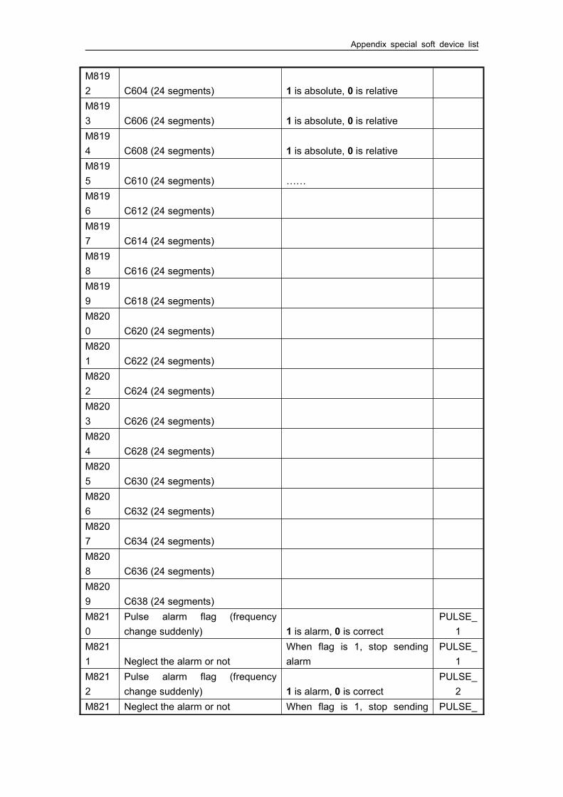
Appendix special soft device list
M8192 C604 (24 segments) 1 is absolute, 0 is relativeM8193 C606 (24 segments) 1 is absolute, 0 is relativeM8194 C608 (24 segments) 1 is absolute, 0 is relativeM8195 C610 (24 segments) ……M8196 C612 (24 segments)M8197 C614 (24 segments)M8198 C616 (24 segments)M8199 C618 (24 segments)M8200 C620 (24 segments)M8201 C622 (24 segments)M8202 C624 (24 segments)M8203 C626 (24 segments)M8204 C628 (24 segments)M8205 C630 (24 segments)M8206 C632 (24 segments)M8207 C634 (24 segments)M8208 C636 (24 segments)M8209 C638 (24 segments)M8210
Pulse alarm flag (frequencychange suddenly) 1 is alarm, 0 is correct
PULSE_1
M8211 Neglect the alarm or not
When flag is 1, stop sendingalarm
PULSE_1
M8212
Pulse alarm flag (frequencychange suddenly) 1 is alarm, 0 is correct
PULSE_2
M821 Neglect the alarm or not When flag is 1, stop sending PULSE_
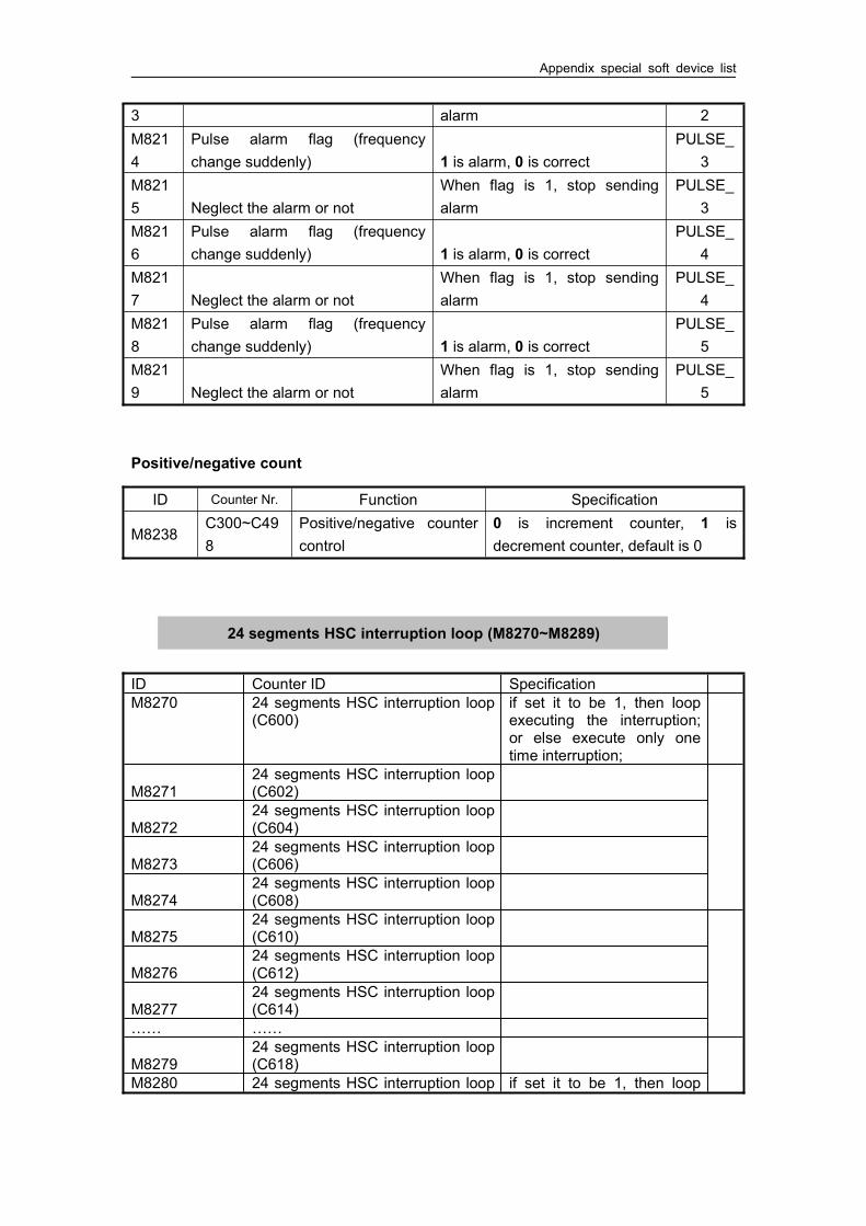
Appendix special soft device list
Positive/negative count
ID Counter ID SpecificationM8270 24 segments HSC interruption loop
(C600)if set it to be 1, then loopexecuting the interruption;or else execute only onetime interruption;
M827124 segments HSC interruption loop(C602)
M827224 segments HSC interruption loop(C604)
M827324 segments HSC interruption loop(C606)
M827424 segments HSC interruption loop(C608)
M827524 segments HSC interruption loop(C610)
M827624 segments HSC interruption loop(C612)
M827724 segments HSC interruption loop(C614)
…… ……
M827924 segments HSC interruption loop(C618)
M8280 24 segments HSC interruption loop if set it to be 1, then loop
3 alarm 2M8214
Pulse alarm flag (frequencychange suddenly) 1 is alarm, 0 is correct
PULSE_3
M8215 Neglect the alarm or not
When flag is 1, stop sendingalarm
PULSE_3
M8216
Pulse alarm flag (frequencychange suddenly) 1 is alarm, 0 is correct
PULSE_4
M8217 Neglect the alarm or not
When flag is 1, stop sendingalarm
PULSE_4
M8218
Pulse alarm flag (frequencychange suddenly) 1 is alarm, 0 is correct
PULSE_5
M8219 Neglect the alarm or not
When flag is 1, stop sendingalarm
PULSE_5
ID Counter Nr. Function Specification
M8238C300~C498
Positive/negative countercontrol
0 is increment counter, 1 isdecrement counter, default is 0
24 segments HSC interruption loop (M8270~M8289)
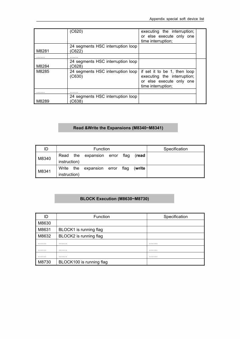
Appendix special soft device list
(C620) executing the interruption;or else execute only onetime interruption;
M828124 segments HSC interruption loop(C622)
…… ……
M828424 segments HSC interruption loop(C628)
M8285 24 segments HSC interruption loop(C630)
if set it to be 1, then loopexecuting the interruption;or else execute only onetime interruption;
…… ……
M828924 segments HSC interruption loop(C638)
ID Function Specification
M8340Read the expansion error flag (readinstruction)
M8341Write the expansion error flag (writeinstruction)
ID Function SpecificationM8630M8631 BLOCK1 is running flagM8632 BLOCK2 is running flag…… …… ………… …… ………… …… ……M8730 BLOCK100 is running flag
Read &Write the Expansions (M8340~M8341)
BLOCK Execution (M8630~M8730)
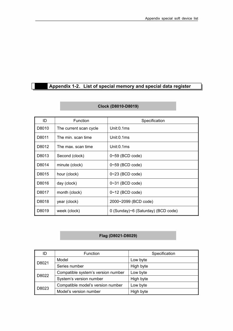
Appendix special soft device list
Appendix 1-2.List of special memory and special data register
ID Function Specification
D8010 The current scan cycle Unit:0.1ms
D8011 The min. scan time Unit:0.1ms
D8012 The max. scan time Unit:0.1ms
D8013 Second (clock) 0~59 (BCD code)
D8014 minute (clock) 0~59 (BCD code)
D8015 hour (clock) 0~23 (BCD code)
D8016 day (clock) 0~31 (BCD code)
D8017 month (clock) 0~12 (BCD code)
D8018 year (clock) 2000~2099 (BCD code)
D8019 week (clock) 0 (Sunday)~6 (Saturday) (BCD code)
ID Function Specification
D8021Model Low byteSeries number High byte
D8022Compatible system’s version number Low byteSystem’s version number High byte
D8023Compatible model’s version number Low byteModel’s version number High byte
Clock (D8010-D8019)
Flag (D8021-D8029)

Appendix special soft device list
D8024Model’s information
Max 5 characters +“\0”
D8025D8026D8027
Suitable program software versionD8028D8029
ID Function SpecificationD8067 Operation error code’s Nr. The error of divide zeroD8068 lock the Nr. of error codeD8069D8070 exceeded scan time Unit 1msD8074 Nr. of offset registers DD8097D8098
Com 1
ID Function specificationD8120D8121D8122 the left data RS232 should sendD8123 Data number RS232 receivedD8126
D8127 Communication error code
7: hardware error8: CRC Parity error9: station number error10: no start code11: no end code12: communication time out
D8128Modbus communication error(the replied message from slaveswhen the master send errors)
0: correct1: don’t support function ID2: address error (overrun address)3: Data error (the number of data)8: saving data error (rewrite Flash)
Error check(D8067-D8098)
Communication (D8120-D8149)
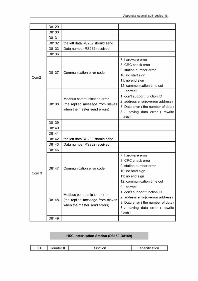
Appendix special soft device list
D8129
Com2
D8130D8131D8132 the left data RS232 should sendD8133 Data number RS232 receivedD8136
D8137 Communication error code
7: hardware error8: CRC check error9: station number error10: no start sign11: no end sign12: communication time out
D8138Modbus communication error(the replied message from slaveswhen the master send errors)
0:correct1: don’t support function ID2: address error(overrun address)3: Data error ( the number of data)8 : saving data error ( rewriteFlash)
D8139
Com 3
D8140D8141D8142 the left data RS232 should sendD8143 Data number RS232 receivedD8146
D8147 Communication error code
7: hardware error8: CRC check error9: station number error10: no start sign11: no end sign12: communication time out
D8148Modbus communication error(the replied message from slaveswhen the master send errors)
0:correct1: don’t support function ID2: address error(overrun address)3: Data error ( the number of data)8 : saving data error ( rewriteFlash)
D8149
ID Counter ID function specification
HSC Interruption Station (D8150-D8169)
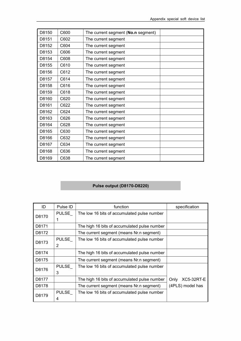
Appendix special soft device list
D8150 C600 The current segment (No.n segment)D8151 C602 The current segmentD8152 C604 The current segmentD8153 C606 The current segmentD8154 C608 The current segmentD8155 C610 The current segmentD8156 C612 The current segmentD8157 C614 The current segmentD8158 C616 The current segmentD8159 C618 The current segmentD8160 C620 The current segmentD8161 C622 The current segmentD8162 C624 The current segmentD8163 C626 The current segmentD8164 C628 The current segmentD8165 C630 The current segmentD8166 C632 The current segmentD8167 C634 The current segmentD8168 C636 The current segmentD8169 C638 The current segment
ID Pulse ID function specification
D8170PULSE_1
The low 16 bits of accumulated pulse number
D8171 The high 16 bits of accumulated pulse numberD8172 The current segment (means Nr.n segment)
D8173PULSE_2
The low 16 bits of accumulated pulse number
D8174 The high 16 bits of accumulated pulse number
D8175 The current segment (means Nr.n segment)
D8176PULSE_3
The low 16 bits of accumulated pulse number
Only XC5-32RT-E(4PLS) model has
D8177 The high 16 bits of accumulated pulse numberD8178 The current segment (means Nr.n segment)
D8179PULSE_4
The low 16 bits of accumulated pulse number
Pulse output (D8170-D8220)
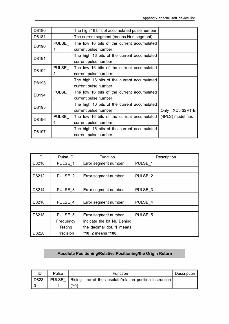
Appendix special soft device list
D8180 The high 16 bits of accumulated pulse numberD8181 The current segment (means Nr.n segment)
D8190PULSE_1
The low 16 bits of the current accumulatedcurrent pulse number
D8191The high 16 bits of the current accumulatedcurrent pulse number
D8192PULSE_2
The low 16 bits of the current accumulatedcurrent pulse number
D8193The high 16 bits of the current accumulatedcurrent pulse number
D8194PULSE_3
The low 16 bits of the current accumulatedcurrent pulse number
Only XC5-32RT-E(4PLS) model has
D8195The high 16 bits of the current accumulatedcurrent pulse number
D8196PULSE_4
The low 16 bits of the current accumulatedcurrent pulse number
D8197The high 16 bits of the current accumulatedcurrent pulse number
ID Pulse ID Function DescriptionD8210 PULSE_1 Error segment number PULSE_1
D8212 PULSE_2 Error segment number PULSE_2
D8214 PULSE_3 Error segment number PULSE_3
D8216 PULSE_4 Error segment number PULSE_4
D8218 PULSE_5 Error segment number PULSE_5
D8220
FrequencyTestingPrecision
indicate the bit Nr. Behindthe decimal dot, 1 means*10, 2 means *100
ID Pulse Function DescriptionD8230
PULSE_1
Rising time of the absolute/relation position instruction(Y0)
Absolute Positioning/Relative Positioning/the Origin Return
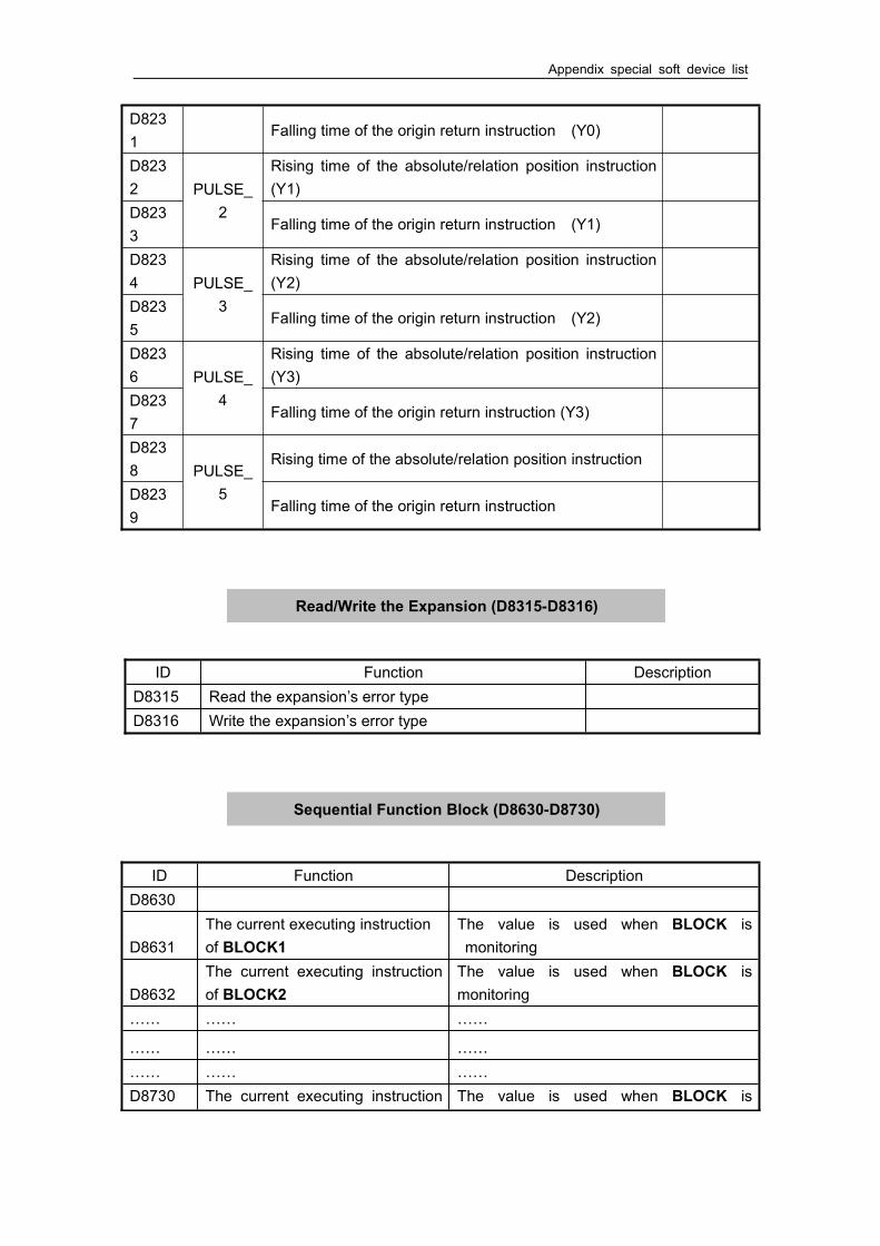
Appendix special soft device list
D8231
Falling time of the origin return instruction (Y0)
D8232 PULSE_
2
Rising time of the absolute/relation position instruction(Y1)
D8233
Falling time of the origin return instruction (Y1)
D8234 PULSE_
3
Rising time of the absolute/relation position instruction(Y2)
D8235
Falling time of the origin return instruction (Y2)
D8236 PULSE_
4
Rising time of the absolute/relation position instruction(Y3)
D8237
Falling time of the origin return instruction (Y3)
D8238 PULSE_
5
Rising time of the absolute/relation position instruction
D8239
Falling time of the origin return instruction
ID Function DescriptionD8315 Read the expansion’s error typeD8316 Write the expansion’s error type
ID Function DescriptionD8630
D8631The current executing instructionof BLOCK1
The value is used when BLOCK ismonitoring
D8632The current executing instructionof BLOCK2
The value is used when BLOCK ismonitoring
…… …… ……
…… …… ………… …… ……D8730 The current executing instruction The value is used when BLOCK is
Read/Write the Expansion (D8315-D8316)
Sequential Function Block (D8630-D8730)
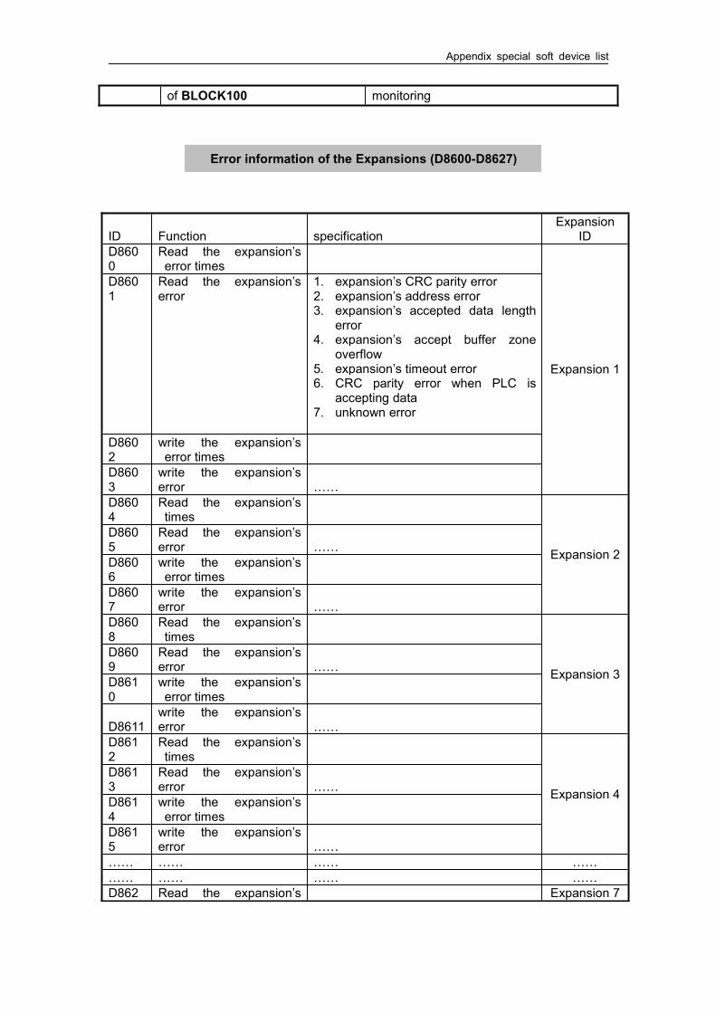
Appendix special soft device list
of BLOCK100 monitoring
ID Function specificationExpansion
IDD8600
Read the expansion’serror times
Expansion 1
D8601
Read the expansion’serror
1. expansion’s CRC parity error2. expansion’s address error3. expansion’s accepted data length
error4. expansion’s accept buffer zone
overflow5. expansion’s timeout error6. CRC parity error when PLC is
accepting data7. unknown error
D8602
write the expansion’serror times
D8603
write the expansion’serror ……
D8604
Read the expansion’stimes
Expansion 2
D8605
Read the expansion’serror ……
D8606
write the expansion’serror times
D8607
write the expansion’serror ……
D8608
Read the expansion’stimes
Expansion 3
D8609
Read the expansion’serror ……
D8610
write the expansion’serror times
D8611write the expansion’serror ……
D8612
Read the expansion’stimes
Expansion 4
D8613
Read the expansion’serror ……
D8614
write the expansion’serror times
D8615
write the expansion’serror ……
…… …… …… ………… …… …… ……D862 Read the expansion’s Expansion 7
Error information of the Expansions (D8600-D8627)

Appendix special soft device list
Appendix 1-3.ID List of the Expansions
Take the first expansion module as the example:
Channel
ADsignal
DAsignal
PIDOutputvalue
PIDrun/stopbit
Set value
PID parameter: Kp, Ki,Kd, control rangeDiff、Death range
deathXC-E8AD0CH ID100 - ID108 Y100 QD100
Kp-----QD108Ki------QD109Kd-----QD110Diff----QD111Death--QD112
1CH ID101 - ID109 Y101 QD1012CH ID102 - ID110 Y102 QD1023CH ID103 - ID111 Y103 QD1034CH ID104 - ID112 Y104 QD1045CH ID105 - ID113 Y105 QD1056CH ID106 - ID114 Y106 QD1067CH ID107 - ID115 Y107 QD107XC-E4AD2DA0CH ID100 - ID104 Y100 QD102
Kp-----QD106Ki------QD107Kd-----QD108Diff----QD109Death--QD110
1CH ID101 - ID105 Y101 QD1032CH ID102 - ID106 Y102 QD1043CH ID103 - ID107 Y103 QD1050CH - QD100 - - -1CH - QD101 - - -XC-E4AD0CH ID100 - ID104 Y100 QD100 Kp-----QD104
Ki-----QD105Kd-----QD106Diff---QD107Death--QD108
1CH ID101 - ID105 Y101 QD1012CH ID102 - ID106 Y102 QD102
3CH ID103 - ID107 Y103 QD103
XC-E4DA
CH Nr. Exp. 1 Exp. 2 Exp. 3 Exp. 4 Exp. 5 Exp. 6 Exp. 7
0CH QD100 QD200 QD300 QD400 QD500 QD600 QD7001CH QD101 QD201 QD301 QD401 QD501 QD601 QD7012CH QD102 QD202 QD302 QD402 QD502 QD602 QD7023CH QD103 QD203 QD303 QD403 QD503 QD603 QD703
4 timesD8625
Read the expansion’serror ……
D8626
write the expansion’serror times
D8627
write the expansion’serror ……
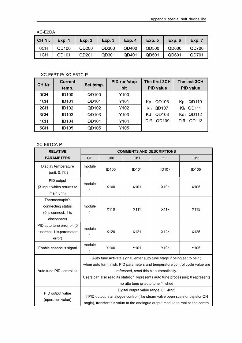
Appendix special soft device list
XC-E2DA
CH Nr. Exp. 1 Exp. 2 Exp. 3 Exp. 4 Exp. 5 Exp. 6 Exp. 7
0CH QD100 QD200 QD300 QD400 QD500 QD600 QD7001CH QD101 QD201 QD301 QD401 QD501 QD601 QD701
XC-E6PT-P/ XC-E6TC-P
CH Nr.Currenttemp.
Set temp.PID run/stop
bitThe first 3CHPID value
The last 3CHPID value
0CH ID100 QD100 Y100
Kp:QD106Ki:QD107Kd:QD108Diff:QD109
Kp:QD110Ki:QD111Kd:QD112Diff:QD113
1CH ID101 QD101 Y1012CH ID102 QD102 Y1023CH ID103 QD103 Y1034CH ID104 QD104 Y1045CH ID105 QD105 Y105
XC-E6TCA-PRELATIVE
PARAMETERS
COMMENTS AND DESCRIPTIONS
CH Ch0 Ch1 Ch5
Display temperature
(unit: 0.1℃)
module
1ID100 ID101 ID10× ID105
PID output
(X input which returns to
main unit)
module
1X100 X101 X10× X105
Thermocouple’s
connecting status
(0 is connect, 1 is
disconnect)
module
1X110 X111 X11× X115
PID auto tune error bit (0
is normal, 1 is parameters
error)
module
1X120 X121 X12× X125
Enable channel’s signalmodule
1Y100 Y101 Y10× Y105
Auto tune PID control bit
Auto tune activate signal, enter auto tune stage if being set to be 1;
when auto turn finish, PID parameters and temperature control cycle value are
refreshed, reset this bit automatically.
Users can also read its status; 1 represents auto tune processing; 0 represents
no atto tune or auto tune finished
PID output value
(operation value)
Digital output value range: 0~4095
If PID output is analogue control (like steam valve open scale or thyistor ON
angle), transfer this value to the analogue output module to realize the control
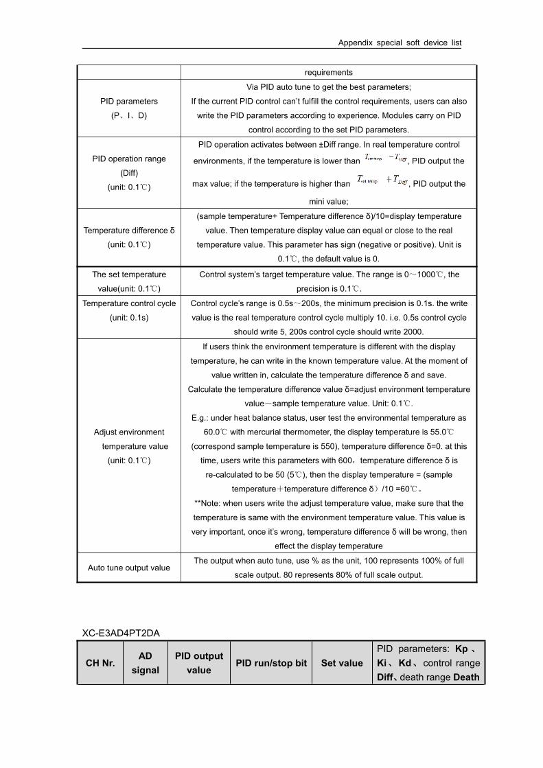
Appendix special soft device list
requirements
PID parameters
(P、I、D)
Via PID auto tune to get the best parameters;
If the current PID control can’t fulfill the control requirements, users can also
write the PID parameters according to experience. Modules carry on PID
control according to the set PID parameters.
PID operation range
(Diff)
(unit: 0.1℃)
PID operation activates between ±Diff range. In real temperature control
environments, if the temperature is lower than , PID output the
max value; if the temperature is higher than , PID output the
mini value;
Temperature difference δ
(unit: 0.1℃)
(sample temperature+ Temperature difference δ)/10=display temperature
value. Then temperature display value can equal or close to the real
temperature value. This parameter has sign (negative or positive). Unit is
0.1℃, the default value is 0.
The set temperature
value(unit: 0.1℃)
Control system’s target temperature value. The range is 0~1000℃, the
precision is 0.1℃.
Temperature control cycle
(unit: 0.1s)
Control cycle’s range is 0.5s~200s, the minimum precision is 0.1s. the write
value is the real temperature control cycle multiply 10. i.e. 0.5s control cycle
should write 5, 200s control cycle should write 2000.
Adjust environment
temperature value
(unit: 0.1℃)
If users think the environment temperature is different with the display
temperature, he can write in the known temperature value. At the moment of
value written in, calculate the temperature difference δ and save.
Calculate the temperature difference value δ=adjust environment temperature
value-sample temperature value. Unit: 0.1℃.
E.g.: under heat balance status, user test the environmental temperature as
60.0℃ with mercurial thermometer, the display temperature is 55.0℃
(correspond sample temperature is 550), temperature difference δ=0. at this
time, users write this parameters with 600,temperature difference δ is
re-calculated to be 50 (5℃), then the display temperature = (sample
temperature+temperature difference δ)/10 =60℃。
**Note: when users write the adjust temperature value, make sure that the
temperature is same with the environment temperature value. This value is
very important, once it’s wrong, temperature difference δ will be wrong, then
effect the display temperature
Auto tune output valueThe output when auto tune, use % as the unit, 100 represents 100% of full
scale output. 80 represents 80% of full scale output.
XC-E3AD4PT2DA
CH Nr.AD
signalPID outputvalue
PID run/stop bit Set valuePID parameters: Kp 、
Ki、Kd、control rangeDiff、death range Death

Appendix special soft device list
0CH ID100 ID107 Y100 QD102
Kp------- QD109Ki------- QD110Kd------- QD111Diff------ QD112Death---- QD113
1CH ID101 ID108 Y101 QD103
2CH ID102 ID109 Y102 QD104
CH Nr.PT
signalPID outputvalue
PID run/stop bit Set value
3CH ID103 ID110 Y103 QD105
4CH ID104 ID111 Y104 QD106
5CH ID105 ID112 Y105 QD107
6CH ID106 ID113 Y106 QD108
CH Nr.DA
signal- - -
-0CH QD100 - - -1CH QD101 - - -
XC-E2AD2PT2DARELATIVE
PARAMETERS
COMMENTS AND DESCRIPTIONS
CH PT0(0.01℃) PT1(0.01℃) AD0 AD1
Display temperature
(unit: 0.1℃)module 1
ID100 ID101 ID102 ID103
PID output
(X input which
returns to main unit)
module 1
X100 X101 X102 X103
Connecting status
(0 is connect, 1 is
disconnect)
module 1
X110 X111 X112 X113
PID auto tune error
bit (0 is normal, 1 is
parameters error)
module 1
X120 X121 X122 X123
Enable channel’s
signalmodule 1
Y100 Y101 Y102 Y103
Auto tune PID
control bit
Auto tune activate signal, enter auto tune stage if being set to be 1;
when auto turn finish, PID parameters and temperature control cycle value are
refreshed, reset this bit automatically.
Users can also read its status; 1 represents auto tune processing; 0 represents no
atto tune or auto tune finished
PID output value
(operation value)
Digital output value range: 0~4095
If PID output is analogue control (like steam valve open scale or thyistor ON angle),
transfer this value to the analogue output module to realize the control requirements
Appendix special soft device list
PID parameters
(P、I、D)
Via PID auto tune to get the best parameters;
If the current PID control can’t fulfill the control requirements, users can also write
the PID parameters according to experience. Modules carry on PID control
according to the set PID parameters.
PID operation range
(Diff)
(unit: 0.1℃)
PID operation activates between ±Diff range. In real temperature control
environments, if the temperature is lower than , PID output the max
value; if the temperature is higher than , PID output the mini value;
Temperature
difference δ
(unit: 0.1℃)
(sample temperature+ Temperature difference δ)/10=display temperature value.
Then temperature display value can equal or close to the real temperature value.
This parameter has sign (negative or positive). Unit is 0.1℃, the default value is 0.
The set temperature
value(unit: 0.1℃)
Control system’s target temperature value. The range is 0~1000℃, the precision is
0.1℃.
Temperature control
cycle (unit: 0.1s)
Control cycle’s range is 0.5s~200s, the minimum precision is 0.1s. the write value
is the real temperature control cycle multiply 10. i.e. 0.5s control cycle should write
5, 200s control cycle should write 2000.
Real value
(unit: 0.1℃)
If users think the environment temperature is different with the display temperature,
he can write in the known temperature value. At the moment of value written in,
calculate the temperature difference δ and save.
Calculate the temperature difference value δ=adjust environment temperature
value-sample temperature value. Unit: 0.1℃.
E.g.: under heat balance status, user test the environmental temperature as 60.0℃
with mercurial thermometer, the display temperature is 55.0℃ (correspond sample
temperature is 550), temperature difference δ=0. at this time, users write this
parameters with 600,temperature difference δ is re-calculated to be 50 (5℃), then
the display temperature = (sample temperature+temperature difference δ)/10
=60℃。
**Note: when users write the adjust temperature value, make sure that the
temperature is same with the environment temperature value. This value is very
important, once it’s wrong, temperature difference δ will be wrong, then effect the
display temperature
Auto tune output
value
The output when auto tune, use % as the unit, 100 represents 100% of full scale
output. 80 represents 80% of full scale output.
Appendix 1-4.Special Flash Register List
1、 I filterID Function Initial Value DescriptionFD8000 input filter time of X port 10 Unit: msFD8002 0FD8003 0…… 0
Appendix special soft device list
FD8009 0
2、 I mappingID Function Initial value DescriptionFD8010
X00 corresponds withI**
0 X0 corresponds with number ofinput image I**
FD8011X01 corresponds withI**
1 Initial values are all decimal
FD8012
X02 corresponds withI**
2
…… ……FD8073
X77 corresponds withI**
63
3、O mapping
ID FunctionInitialvalue
Description
FD8074 Y00 corresponds with I** 0 Y0 corresponds with thenumber of output image O**
FD8075 Y01 corresponds with I** 1 Initial value are all decimalFD8076 Y02 corresponds with I** 2…… ……FD8137 Y77 corresponds with I** 63
4、 I propertyID function Initial value DescriptionFD8138 X00
propertyall be 0 0: positive logic;
others: negative logicFD8139 X01
propertyFD8140 X02
property…… ……FD8201 X77
property
5、power-off retentive area of soft components
Softcomponent
FDREGISTER
FUNCTIONDefaultvalue
Power-offretentive range
XC1series
D FD8202Start tag of D power offretentive area
100 D100~D149
M FD8203Start tag of M poweroff retentive area
200 M200~M319
Appendix special soft device list
T FD8204Start tag of T power offretentive area
640 -
C FD8205Start tag of C power offretentive area
320 C320~C631
S FD8206Start tag of S power offretentive area
512 -
XC2series
D FD8202Start tag of D power offretentive area
4000 D4000~D4999
M FD8203Start tag of M poweroff retentive area
3000 M3000~M7999
T FD8204Start tag of T power offretentive area
640 -
C FD8205Start tag of C power offretentive area
320 C320~C639
S FD8206Start tag of S power offretentive area
512 S512~S1023
XC3series
D FD8202Start tag of D power offretentive area
4000 D4000~D7999
M FD8203Start tag of M poweroff retentive area
3000 M3000~M7999
T FD8204Start tag of T power offretentive area
640 -
C FD8205Start tag of C power offretentive area
320 C320~C639
S FD8206Start tag of S power offretentive area
512 S512~S1023
ED FD8207Start tag of ED poweroff retentive area
0 ED0~ED16383
XC5series
D FD8202Start tag of D power offretentive area
4000 D4000~D7999
M FD8203Start tag of M poweroff retentive area
4000 M4000~M7999
T FD8204Start tag of T power offretentive area
640 -
C FD8205Start tag of C power offretentive area
320 C320~C639
S FD8206Start tag of S power offretentive area
512 S512~S1023
ED FD8207Start tag of ED poweroff retentive area
0 ED0~ED36863
XCMseries
D FD8202Start tag of D power offretentive area
4000 D4000~D4999
Appendix special soft device list
M FD8203Start tag of M poweroff retentive area
3000 M3000~M7999
T FD8204Start tag of T power offretentive area
640 -
C FD8205Start tag of C power offretentive area
320 C320~C639
S FD8206Start tag of S power offretentive area
512 S512~S1023
ED FD8207Start tag of ED poweroff retentive area
0 ED0~ED36863
6、Communication
COM1
ID Function Initial Description
FD8210
Communicate Mode(station number)
1255 (FF) is free mode,1~254 is modbus stationnumber
FD8211
Communicate format 8710Baud rate, Data bit, stop bit,parity
FD8212
Judgment time of ASCtimeout
3Unit ms, if set to be 0, it meansno timeout waiting
FD8213
Judgment time of replytimeout
300Unit ms, if set to be 0, it meansno timeout waiting
FD8214
Start ASC 0 High 8 bits invalid
FD8215
End ASC 0 High 8 bits invalid
FD8216
Free format setting 08/16 bits buffer;With/without start bit,With/without stop bit
COM2
FD8220
Communicate Mode(station number)
8710255 (FF) is free mode,1~254 is modbus stationnumber
FD8221
Communicate format 3Baud rate, Data bit, stop bit,parity
FD8222
Judgment time of ASCtimeout
300Unit ms, if set to be 0, it meansno timeout waiting
FD8223
Judgment time of replytimeout
0Unit ms, if set to be 0, it meansno timeout waiting
FD8224
Start ASC 0 High 8 bits invalid
FD8225
End ASC 0 High 8 bits invalid
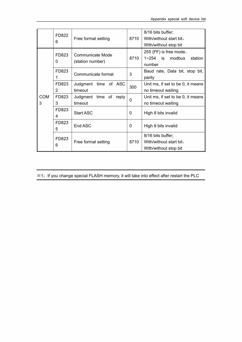
Appendix special soft device list
FD8226
Free format setting 87108/16 bits buffer;With/without start bit,With/without stop bit
COM3
FD8230
Communicate Mode(station number)
8710255 (FF) is free mode,1~254 is modbus stationnumber
FD8231
Communicate format 3Baud rate, Data bit, stop bit,parity
FD8232
Judgment time of ASCtimeout
300Unit ms, if set to be 0, it meansno timeout waiting
FD8233
Judgment time of replytimeout
0Unit ms, if set to be 0, it meansno timeout waiting
FD8234
Start ASC 0 High 8 bits invalid
FD8235
End ASC 0 High 8 bits invalid
FD8236
Free format setting 87108/16 bits buffer;With/without start bit,With/without stop bit
※1:If you change special FLASH memory, it will take into effect after restart the PLC
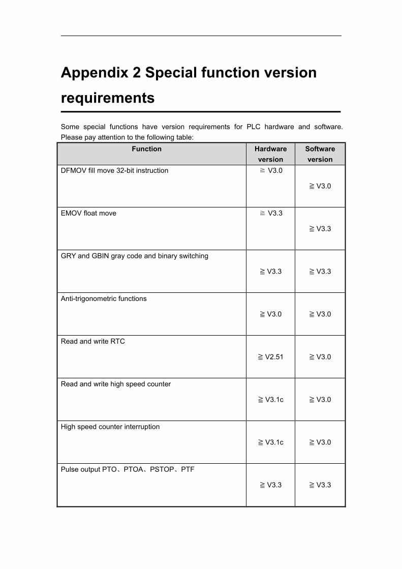
Appendix 2 Special function versionrequirements
Some special functions have version requirements for PLC hardware and software.Please pay attention to the following table:
Function Hardwareversion
Softwareversion
DFMOV fill move 32-bit instruction ≧ V3.0 ≧ V3.0
EMOV float move ≧ V3.3 ≧ V3.3
GRY and GBIN gray code and binary switching ≧ V3.3 ≧ V3.3
Anti-trigonometric functions ≧ V3.0 ≧ V3.0
Read and write RTC ≧ V2.51 ≧ V3.0
Read and write high speed counter ≧ V3.1c ≧ V3.0
High speed counter interruption ≧ V3.1c ≧ V3.0
Pulse output PTO、PTOA、PSTOP、PTF ≧ V3.3 ≧ V3.3

RCVST serial port release for free format communication ≧ V3.1e ≧ V3.1f
Read precise timer ≧ V3.0e ≧ V3.0
Stop precise timer ≧ V3.0e ≧ V3.0
C function block ≧ V3.0c ≧ V3.0
PID function ≧ V3.0 ≧ V3.0
Sequence block ≧ V3.2 ≧ V3.1h
Connect to T-BOX, XC-TBOX-BD ≧ V3.0g
V3.0f or≧ V3.3f ※1
Connect to G-BOX ≧ V3.0i
≧ V3.0
Connect to XC-SD-BD ≧ V3.2
≧ V3.2
Read and write XC-E6TCA-P, XC-E2AD2PT3DA,XC-E2AD2PT2DA ≧ V3.1f
≧ V3.1b

ED extension register ≧ V3.0
≧ V3.0
※1: Old version of T-BOX, T-BOX-BD: software v3.0f; new version of T-BOX, T-BOX-BD (made after Oct,
2010): software v3.3f and higher.

Appendix 3 Applied instruction
Instruction FunctionXC series PLC
Chapter
XC1
XC2
XC3
XC5
XCMXCC
FlowCJ Condition Jump ● ● ● ● ● ● 4-3-1CALL Call subroutine ● ● ● ● ● ● 4-3-2SRET Subroutine return ● ● ● ● ● ● 4-3-2STL Flow start ● ● ● ● ● ● 4-3-3STLE Flow end ● ● ● ● ● ● 4-3-3
SET Open the assigned flow,close the current flow ● ● ● ● ● ● 4-3-3
STOpen the assigned flow,not close the currentflow
● ● ● ● ● ● 4-3-3
FOR Start of a FOR-NEXTloop ● ● ● ● ● ● 4-3-4
NEXT END of a FOR-NEXTloop ● ● ● ● ● ● 4-3-4
FEND End of main program ● ● ● ● ● ● 4-3-5END Program end ● ● ● ● ● ● 4-3-5Data comparisonLD= LD activate if (S1)= (S2) ● ● ● ● ● ● 4-4-1LD> LD activate if (S1)> (S2) ● ● ● ● ● ● 4-4-1LD< LD activate if (S1)< (S2) ● ● ● ● ● ● 4-4-1LD<> LD activate if(S1)≠(S2) ● ● ● ● ● ● 4-4-1LD<= LD activate if(S1) <=
(S2) ● ● ● ● ● ● 4-4-1
LD>= LD activate if(S1) >=(S2) ● ● ● ● ● ● 4-4-1
AND= AND activate if (S1)=(S2) ● ● ● ● ● ● 4-4-2
AND> AND activate if (S1)>(S2) ● ● ● ● ● ● 4-4-2
AND< AND activate if (S1)<(S2) ● ● ● ● ● ● 4-4-2
AND<> AND activateif(S1)≠(S2) ● ● ● ● ● ● 4-4-2
AND<= AND activate if(S1) <=(S2) ● ● ● ● ● ● 4-4-2
AND>= AND activate if(S1) >=(S2) ● ● ● ● ● ● 4-4-2
OR= OR activate if (S1)= (S2) ● ● ● ● ● ● 4-4-3
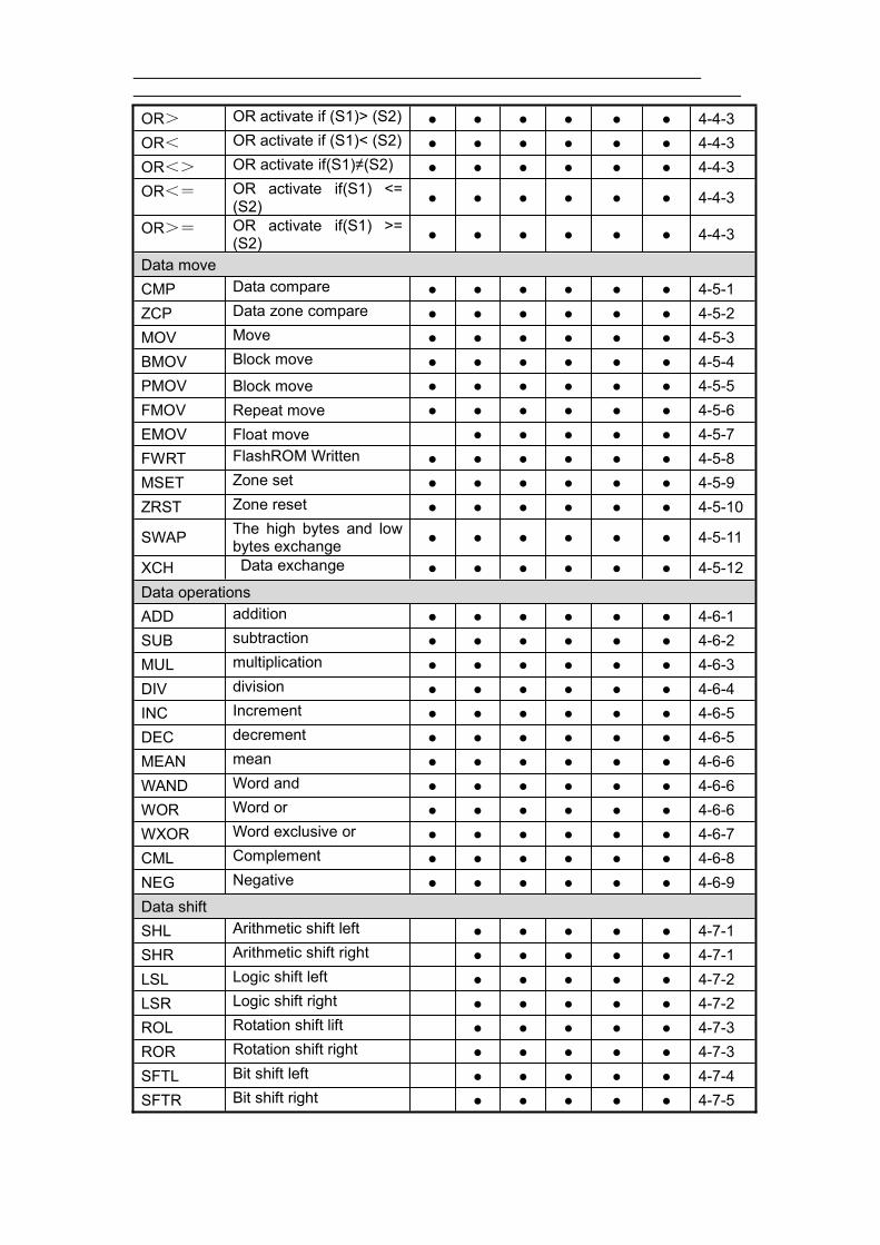
OR> OR activate if (S1)> (S2) ● ● ● ● ● ● 4-4-3OR< OR activate if (S1)< (S2) ● ● ● ● ● ● 4-4-3OR<> OR activate if(S1)≠(S2) ● ● ● ● ● ● 4-4-3OR<= OR activate if(S1) <=
(S2) ● ● ● ● ● ● 4-4-3
OR>= OR activate if(S1) >=(S2) ● ● ● ● ● ● 4-4-3
Data moveCMP Data compare ● ● ● ● ● ● 4-5-1ZCP Data zone compare ● ● ● ● ● ● 4-5-2MOV Move ● ● ● ● ● ● 4-5-3BMOV Block move ● ● ● ● ● ● 4-5-4PMOV Block move ● ● ● ● ● ● 4-5-5FMOV Repeat move ● ● ● ● ● ● 4-5-6EMOV Float move ● ● ● ● ● 4-5-7FWRT FlashROM Written ● ● ● ● ● ● 4-5-8MSET Zone set ● ● ● ● ● ● 4-5-9ZRST Zone reset ● ● ● ● ● ● 4-5-10
SWAP The high bytes and lowbytes exchange ● ● ● ● ● ● 4-5-11
XCH Data exchange ● ● ● ● ● ● 4-5-12Data operationsADD addition ● ● ● ● ● ● 4-6-1SUB subtraction ● ● ● ● ● ● 4-6-2MUL multiplication ● ● ● ● ● ● 4-6-3DIV division ● ● ● ● ● ● 4-6-4INC Increment ● ● ● ● ● ● 4-6-5DEC decrement ● ● ● ● ● ● 4-6-5MEAN mean ● ● ● ● ● ● 4-6-6WAND Word and ● ● ● ● ● ● 4-6-6WOR Word or ● ● ● ● ● ● 4-6-6WXOR Word exclusive or ● ● ● ● ● ● 4-6-7CML Complement ● ● ● ● ● ● 4-6-8NEG Negative ● ● ● ● ● ● 4-6-9Data shiftSHL Arithmetic shift left ● ● ● ● ● 4-7-1SHR Arithmetic shift right ● ● ● ● ● 4-7-1LSL Logic shift left ● ● ● ● ● 4-7-2LSR Logic shift right ● ● ● ● ● 4-7-2ROL Rotation shift lift ● ● ● ● ● 4-7-3ROR Rotation shift right ● ● ● ● ● 4-7-3SFTL Bit shift left ● ● ● ● ● 4-7-4SFTR Bit shift right ● ● ● ● ● 4-7-5

WSFL Word shift left ● ● ● ● ● 4-7-6WSFR Word shift right ● ● ● ● ● 4-7-7Data convert
WTDSingle word integerconvert to double wordinteger
● ● ● ● ● 4-8-1
FLT 16 bits integer convert tofloat ● ● ● ● ● 4-8-2
DFLT 32 bits integer convert tofloat ● ● ● ● ● 4-8-2
FLTD 64 bits integer convert tofloat ● ● ● ● ● 4-8-2
INT Float convert to integer ● ● ● ● ● 4-8-3BIN BCD convert to binary ● ● ● ● ● 4-8-4BCD Binary convert to BCD ● ● ● ● ● 4-8-5ASCI Hex convert to ASCI ● ● ● ● ● 4-8-6HEX ASCI convert to Hex ● ● ● ● ● 4-8-7DECO Coding ● ● ● ● ● 4-8-8ENCO High bit coding ● ● ● ● ● 4-8-9ENCOL Low bit coding ● ● ● ● ● 4-8-10GRY Binary to gray code ● ● ● ● ● 4-8-11GBIN Gray code to binary ● ● ● ● ● 4-8-12Float operationECMP Float compare ● ● ● ● ● 4-9-1EZCP Float zone compare ● ● ● ● ● 4-9-2EADD Float addition ● ● ● ● ● 4-9-3ESUB Float subtraction ● ● ● ● ● 4-9-4EMUL Float multiplication ● ● ● ● ● 4-9-5EDIV Float division ● ● ● ● ● 4-9-6ESQR Float square root ● ● ● ● ● 4-9-7SIN Sine ● ● ● ● ● 4-9-8COS Cosine ● ● ● ● ● 4-9-9TAN tangent ● ● ● ● ● 4-9-10ASIN Float arcsin ● ● ● ● ● 4-9-11ACOS Float arccos ● ● ● ● ● 4-9-12ATAN Float arctan ● ● ● ● ● 4-9-13ClockTRD Read RTC data ● ● ● ● ● 4-10-1TWR Set RTC data ● ● ● ● ● 4-10-2High speed counter
HSCR Read high speedcounter value ● ● ● ● ● 5-6-1
HSCW Write high speedcounter value ● ● ● ● ● 5-6-2
Pulse output
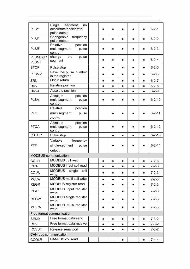
PLSYSingle segment noaccelerate/deceleratepulse output
● ● ● ● ● 6-2-1
PLSF Changeable frequencypulse output ● ● ● ● ● 6-2-2
PLSRRelative positionmulti-segment pulsecontrol
● ● ● ● ● 6-2-3
PLSNEXT/PLSNT
change the pulsesegment ● ● ● ● ● 6-2-4
STOP Pulse stop ● ● ● ● ● 6-2-5
PLSMV Save the pulse numberin the register ● ● ● ● ● 6-2-6
ZRN Origin return ● ● ● ● ● 6-2-7DRVI Relative position ● ● ● ● ● 6-2-8DRVA Absolute position ● ● ● ● ● 6-2-9
PLSAAbsolute positionmulti-segment pulsecontrol
● ● ● ● ● 6-2-10
PTORelative positionmulti-segment pulsecontrol
● ● ● ● 6-2-11
PTOAAbsolute positionmulti-segment pulsecontrol
● ● ● ● 6-2-12
PSTOP Pulse stop ● ● ● ● 6-2-13
PTFVariable frequencysingle-segment pulseoutput
● ● ● ● 6-2-14
MODBUS communicationCOLR MODBUS coil read ● ● ● ● ● 7-2-3INPR MODBUS input coil read ● ● ● ● ● 7-2-3
COLW MODBUS single coilwrite ● ● ● ● ● 7-2-3
MCLW MODBUS multi coil write ● ● ● ● ● 7-2-3REGR MODBUS register read ● ● ● ● ● 7-2-3
INRR MODBUS input registerwrite ● ● ● ● ● 7-2-3
REGW MODBUS single registerwrite ● ● ● ● ● 7-2-3
MRGW MODBUS multi registerwrite ● ● ● ● ● 7-2-3
Free format communicationSEND Free format data send ● ● ● ● ● 7-3-2RCV Free format data receive ● ● ● ● ● 7-3-2RCVST Release serial port ● ● ● ● ● 7-3-2CAN-bus communicationCCOLR CANBUS coil read ● ● 7-4-4

CCOLW CANBUS coil write ● ● 7-4-4CREGR CANBUS register read ● ● 7-4-4CREGW CANBUS register write ● ● 7-4-4OtherPID PID control ● ● ● ● ● 8-2NAME_C Call the C function ● ● ● ● ● 9-2SBSTOP Pause BLOCK running ● ● ● ● ● 10-6
SBGOONContinue runningBLOCK
● ● ● ● ● 10-6
WAIT Wait ● ● ● ● ● 10-3-4
PWMPulse output with certainfrequency and duty ratio
● ● ● ● ● 11-1
FRQM Frequency test ● ● ● ● 11-2STR Precise timer ● ● ● ● ● 11-3
STRRRead precise timerregister
● ● ● ● ● 11-3
STRS Stop the precise timer ● ● ● ● ● 11-3EI Interruption enable ● ● ● ● ● 11-4DI Interruption disable ● ● ● ● ● 11-4IRET Interruption return ● ● ● ● ● 11-4Read write moduleFROM※1 Read the module ● ● ● ● ●TO※1 Write the module ● ● ● ● ●
※1: Please refer to XC series expansion module manual.
※2: “●” means this model supports the present instruction.
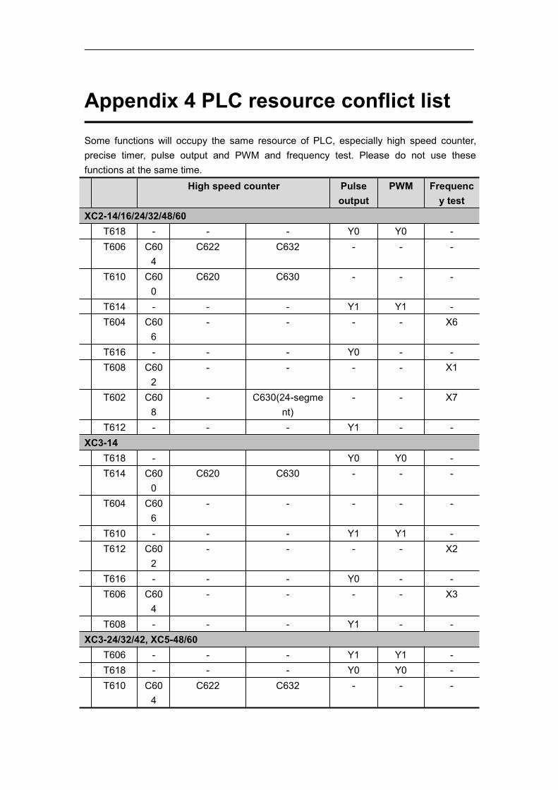
Appendix 4 PLC resource conflict list
Some functions will occupy the same resource of PLC, especially high speed counter,precise timer, pulse output and PWM and frequency test. Please do not use thesefunctions at the same time.
High speed counter Pulseoutput
PWM Frequency test
XC2-14/16/24/32/48/60T618 - - - Y0 Y0 -T606 C60
4C622 C632 - - -
T610 C600
C620 C630 - - -
T614 - - - Y1 Y1 -T604 C60
6- - - - X6
T616 - - - Y0 - -T608 C60
2- - - - X1
T602 C608
- C630(24-segment)
- - X7
T612 - - - Y1 - -XC3-14
T618 - Y0 Y0 -T614 C60
0C620 C630 - - -
T604 C606
- - - - -
T610 - - - Y1 Y1 -T612 C60
2- - - - X2
T616 - - - Y0 - -T606 C60
4- - - - X3
T608 - - - Y1 - -XC3-24/32/42, XC5-48/60
T606 - - - Y1 Y1 -T618 - - - Y0 Y0 -T610 C60
4C622 C632 - - -

T614 C600
C620 C630 - - -
T604 C606
C624 C634 - - -
T608 - - - Y1 - -T616 - - - Y0 - -T612 C60
2- - - - X1
T602 C608
- C630(24-segment)
- - X11
T600 - - - - - X12XC3-48/60
- - - - - - -T618 - - - Y0 Y0 -T614 C60
0C620 C630 - - -
T604 C602
C622 C632 - - -
T610 - - - Y1 Y1 -T612 C60
4- - - - X4
T616 - - - Y0 - -T606 C60
6- - - - X5
T600 - - C630(24-segment)
- - -
T608 - - - Y1 - -XC3-19AR-E
T602 - - - - - -T618 - - - Y0 Y0 -T614 C60
0C620 C630 - - -
T604 C602
C622 C632 - - -
T610 - - - - - -T612 C60
4- - - - X4
T616 - - - Y0 - -T606 C60
6- - - - X5
T600 - - C630(24-segment)
- - -

T608 - - - - - -XC5-24/32、XCM-24/32
T614 - - - Y1 Y1 -T618 - - - Y0 Y0 -T610 - - - Y2 Y2 -T606 C60
0C620 C630 - - -
T602 - - - Y3 Y3 -T612 - - - Y1 - -T616 - - - Y0 - -T608 - - - Y2 - -T604 C60
2- C630(24-segme
nt)- - X3
T600 - - - Y3 - -XCM-60
T614 - - - Y1 Y1 -T618 - - - Y0 Y0 -T610 - - - Y2 Y2 -T606 C60
0C620
(24-segment)
C630(24-segment)
- X1
T602 - - - Y3 Y3 -T612 - - - Y0 - -T616 - - - Y1 -T608 - - - Y2 - -T604 C60
2C630
(24-segment)- - -
T600 Y3 - -C604
- C632(24-segment)
- -
C606
- C634(24-segment)
- -
XCC-24/32T616 - - - Y4 Y4 -T618 - - - Y0 Y0 -T614 - - - Y1 Y1 -T612 - - - Y2 Y2 -T610 - - - Y3 Y3 -T606 - - - Y4 - -T608 - - - Y0 -T604 - - - Y1 - -
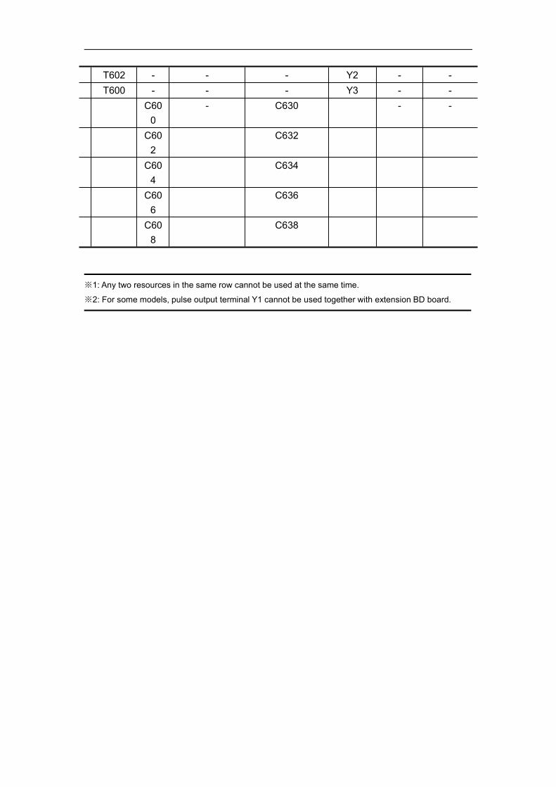
T602 - - - Y2 - -T600 - - - Y3 - -
C600
- C630 - -
C602
C632
C604
C634
C606
C636
C608
C638
※1: Any two resources in the same row cannot be used at the same time.
※2: For some models, pulse output terminal Y1 cannot be used together with extension BD board.

Spectra Technologies


