1SWRU359E–September 2013–Revised September 2015Submit Documentation Feedback
Copyright © 2013–2015, Texas Instruments Incorporated
WL1835MODCOM8B WLAN MIMO and Bluetooth® Module EVM
User's GuideSWRU359E–September 2013–Revised September 2015
WL1835MODCOM8B WLAN MIMO and Bluetooth® ModuleEVM
This user's guide describes how to use the TI WL1835MODCOM8B board to evaluate the performance ofthe TI WL18MODGB module.
Contents1 Warning ....................................................................................................................... 22 Introduction ................................................................................................................... 3
2.1 Features.............................................................................................................. 42.2 Applications.......................................................................................................... 52.3 TI Module Key Benefits ............................................................................................ 5
3 Board Pin Assignment ...................................................................................................... 63.1 Pin Descriptions..................................................................................................... 7
4 Electrical Characteristics.................................................................................................... 95 Approved Antenna Types and Maximum Gain Values ................................................................. 96 On-Board Antenna Configuration ........................................................................................ 10
6.1 VSWR............................................................................................................... 106.2 Efficiency ........................................................................................................... 116.3 Radio Pattern ...................................................................................................... 116.4 ANT1 ................................................................................................................ 126.5 ANT2 ................................................................................................................ 13
7 Circuit Design ............................................................................................................... 157.1 Schematic .......................................................................................................... 157.2 Bill of Materials (BOM)............................................................................................ 16
8 Layout Guidelines .......................................................................................................... 178.1 Board Layout....................................................................................................... 17
List of Figures
1 WL1835MODCOM8B Top View ........................................................................................... 32 Board Top View .............................................................................................................. 63 Board Bottom View .......................................................................................................... 64 Antenna VSWR............................................................................................................. 105 Antenna Efficiency ......................................................................................................... 116 Radio Pattern ............................................................................................................... 117 ANT1 Polarization .......................................................................................................... 128 ANT1 Polarization .......................................................................................................... 129 ANT1 Polarization .......................................................................................................... 1310 ANT2 Polarization .......................................................................................................... 1311 ANT2 Polarization .......................................................................................................... 1412 ANT2 Polarization .......................................................................................................... 1413 Schematic ................................................................................................................... 1514 Layer 1....................................................................................................................... 1715 Layer 2....................................................................................................................... 1716 Layer 3....................................................................................................................... 18
Warning www.ti.com
2 SWRU359E–September 2013–Revised September 2015Submit Documentation Feedback
Copyright © 2013–2015, Texas Instruments Incorporated
WL1835MODCOM8B WLAN MIMO and Bluetooth® Module EVM
17 Layer 4....................................................................................................................... 1818 Module Layout Guidelines (Top Layer).................................................................................. 1919 Module Layout Guidelines (Bottom Layer).............................................................................. 1920 Trace Design for the PCB Layout........................................................................................ 2021 Layer 1 Combined With Layer 2 ......................................................................................... 2022 Top Layer – Antenna and RF Trace Routing Layout Guidelines .................................................... 2123 Bottom Layer – Antenna and RF Trace Routing Layout Guidelines ................................................ 2124 MIMO Antenna Spacing ................................................................................................... 22
List of Tables
1 Approved Antenna Types and Maximum Gain Values ................................................................. 92 BOM.......................................................................................................................... 163 Module Layout Guidelines ................................................................................................ 184 Antenna and RF Trace Routing Layout Guidelines.................................................................... 20
TrademarksWiLink8 is a trademark of Texas Instruments.Bluetooth is a registered trademark of Bluetooth SIG, Inc.Android is a trademark of Google Inc.Linux is a registered trademark of Linux Foundation.Wi-Fi is a registered trademark of Wi-Fi Alliance.
1 WarningThe WL1835MODCOM8B board is tested to comply with ETSI/R&TTE over temperatures from –20°C to85°C.
This board should not be modified to operate in other frequency bands other than what they are designedfor.
FCC Licensing Requirements for the Wi-Fi and Bluetooth Radio Module of the EVM:For evaluation only; not FCC approved for resale. This kit is designed to allow:1. Product developers to evaluate electronic components, circuitry, or software associated with the kit to
determine whether to incorporate such items in a finished product2. Software developers to write software applications for use with the end product. This kit is not a
finished product and when assembled may not be resold or otherwise marketed unless all requiredFCC equipment authorizations are first obtained. Operation is subject to the condition that this productnot cause harmful interference to licensed radio stations and that this product accept harmfulinterference. Unless the assembled kit is designed to operate under part 15, part 18, or part 95 of thischapter, the operator of the kit must operate under the authority of an FCC license holder or mustsecure an experimental authorization under part 5 of this chapter.
Per TI’s Regulatory Compliance Information located in the WL1835ModCOMB8B User’s Guide’s“Evaluation Board/Kit/Module (EVM) Additional Terms,” this EVM cannot be used for production purposesand is explicitly restricted from end-product introduction.
Use of this EVM requires the developer to provide a minimum distance of at least 20 cm from the antennato all persons in order to minimize risk of potential radiation hazards.
CAUTIONDo not leave the EVM powered when unattended.
FCC/IC Regulatory ComplianceFCC Part 15 Class A CompliantIC ICES-003 Class A Compliant
www.ti.com Introduction
3SWRU359E–September 2013–Revised September 2015Submit Documentation Feedback
Copyright © 2013–2015, Texas Instruments Incorporated
WL1835MODCOM8B WLAN MIMO and Bluetooth® Module EVM
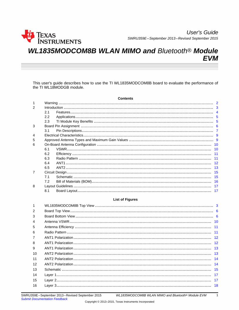
2 IntroductionThe WL1835MODCOM8B device is a Wi-Fi® MIMO, Bluetooth, and Bluetooth Low Energy (BLE) moduleboard with the TI WL18MODGB module. WL18MODGB is built-in TI WL1835 IEEE 802.11 b/g/n andBluetooth 4.0 solutions to provide the best Wi-Fi and Bluetooth coexistence interoperability and power-saving technologies from TI.
Figure 1. WL1835MODCOM8B Top View
IC ID: 451I-WL1835COM
This device complies with Industry Canada licence-exempt RSS standard(s). Operation is subject to the following two conditions: (1) this device may not cause interference, and (2) this device must accept any interference, including that may cause undesired operation of the device.
FCC ID: Z64-WL1835COM
This device complies with part 15 of the FCC Rules. Operation is subject to the following two conditions: (1) This device may not cause harmful interference, and (2) this device must accept any interference received, including interference that may cause undesired operation.
Introduction www.ti.com
4 SWRU359E–September 2013–Revised September 2015Submit Documentation Feedback
Copyright © 2013–2015, Texas Instruments Incorporated
WL1835MODCOM8B WLAN MIMO and Bluetooth® Module EVM
(continued)
2.1 Features• WLAN, Bluetooth, BLE on a module board• 100-pin board card• Dimension 76.0 mm(L) x 31.0 mm(W)• WLAN 2.4 GHz SISO (20- and 40-MHz channels), 2.4-GHz MIMO (20-MHz channels)• Support for BLE dual mode• Seamless integration with TI Sitara and other application processors• Design for TI AM335X general-purpose EVM• WLAN and Bluetooth, BLE cores are software and hardware compatible with prior WL127x, WL128x
and CC256x offerings, for smooth migration to device.• Shared HCI transport for Bluetooth and BLE over UART and SDIO for WLAN.• Wi-Fi / Bluetooth single antenna co-existence• Built-in chip antenna• Optional U.FL RF connector for external 2.4-GHz band antenna• Direct connection to battery using external switching mode power supply supporting 4.8-V to 2.9-V
operation• VIO in the 1.8-V domain
www.ti.com Introduction
5SWRU359E–September 2013–Revised September 2015Submit Documentation Feedback
Copyright © 2013–2015, Texas Instruments Incorporated
WL1835MODCOM8B WLAN MIMO and Bluetooth® Module EVM
2.2 Applications• Internet of Things Multimedia• Home Electronics• Home Appliances and White Goods• Industrial and Home Automation• Smart Gateway and Metering• Video Conferencing• Video Camera and Security
2.3 TI Module Key Benefits• Reduces Design Overhead: Single WiLink8™ Module Scales Across Wi-Fi and Bluetooth.• WLAN High Throughput: 80 Mbps (TCP), 100 Mbps (UDP)• Bluetooth 4.0 + BLE (Smart Ready)• Wi-Fi-Bluetooth Single Antenna Coexistence• Low Power (30–50% Less than Previous Generation)• Available as Easy-to-Use FCC, ETSI, and Telec Certified Module• Lower Manufacturing Costs, Saving Board Space and Minimizing RF Expertise• AM335x Linux® and Android™ Reference Platform Accelerates Customer Development and Time to
Market
U1
WL18MODGB
Board Pin Assignment www.ti.com
6 SWRU359E–September 2013–Revised September 2015Submit Documentation Feedback
Copyright © 2013–2015, Texas Instruments Incorporated
WL1835MODCOM8B WLAN MIMO and Bluetooth® Module EVM
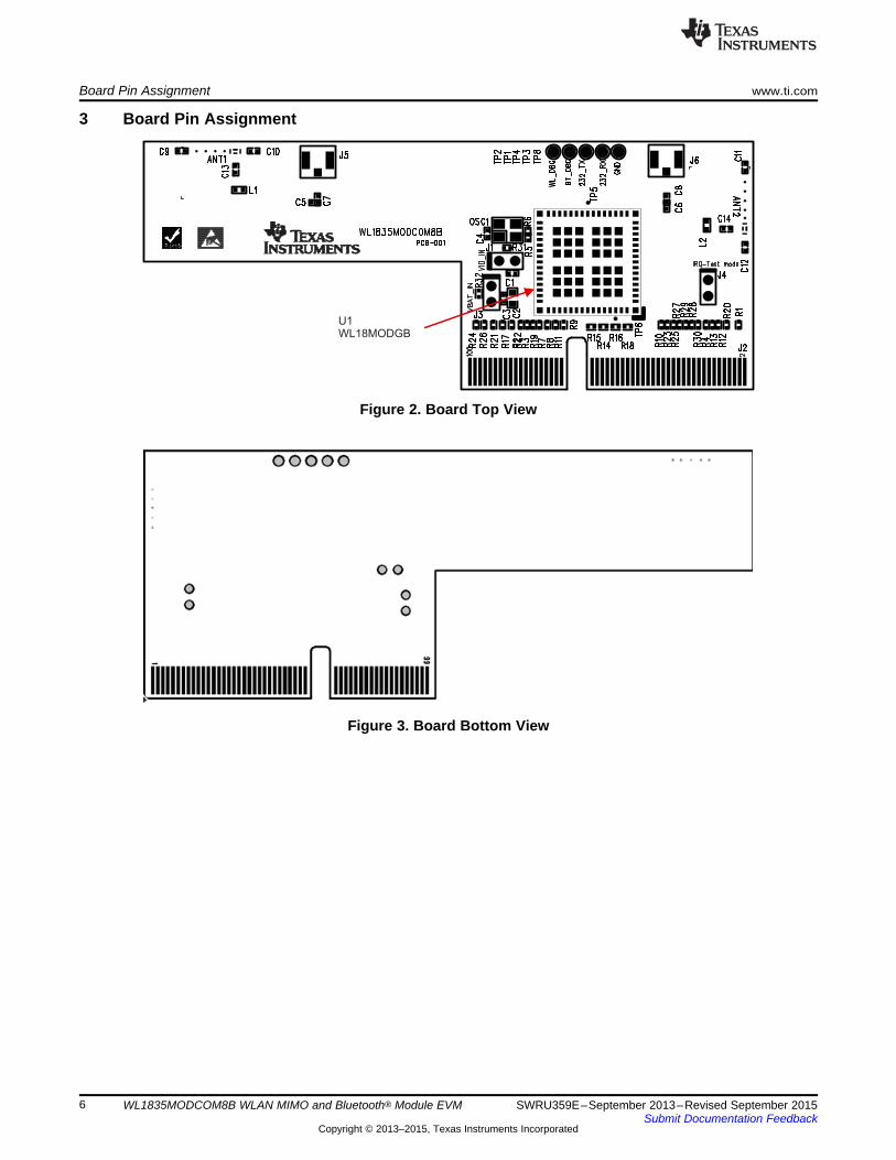
3 Board Pin Assignment
Figure 2. Board Top View
Figure 3. Board Bottom View
www.ti.com Board Pin Assignment
7SWRU359E–September 2013–Revised September 2015Submit Documentation Feedback
Copyright © 2013–2015, Texas Instruments Incorporated
WL1835MODCOM8B WLAN MIMO and Bluetooth® Module EVM
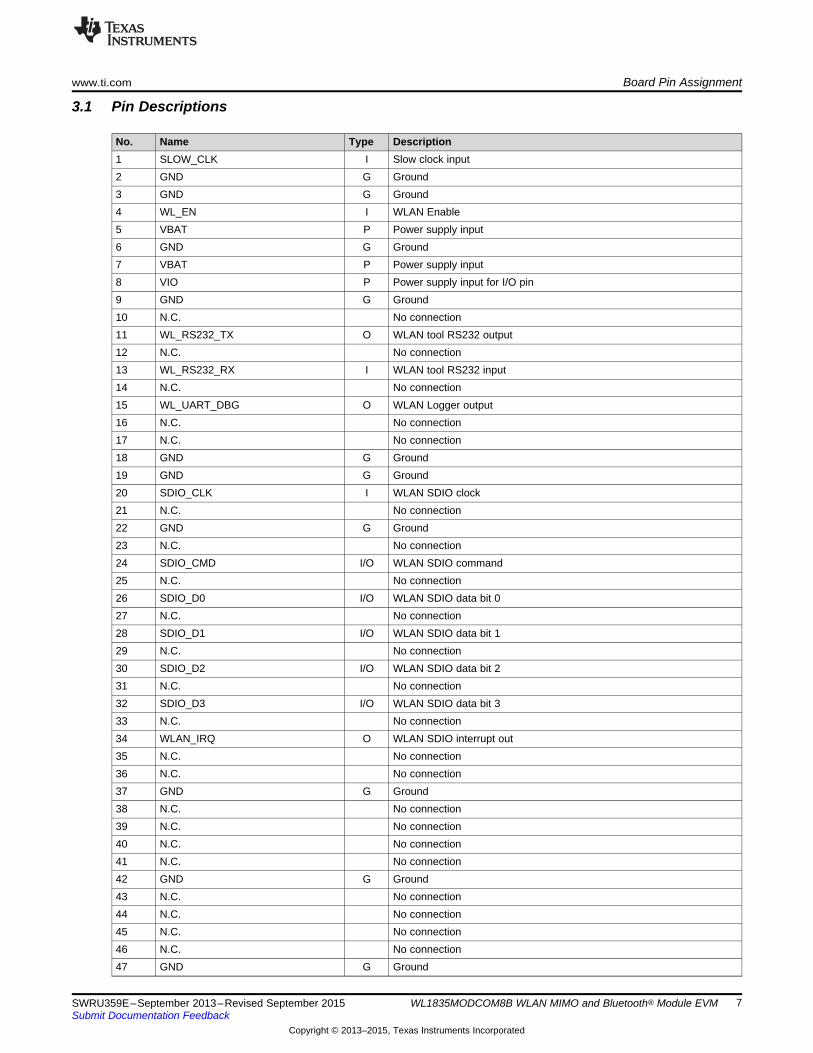
3.1 Pin Descriptions
No. Name Type Description1 SLOW_CLK I Slow clock input2 GND G Ground3 GND G Ground4 WL_EN I WLAN Enable5 VBAT P Power supply input6 GND G Ground7 VBAT P Power supply input8 VIO P Power supply input for I/O pin9 GND G Ground10 N.C. No connection11 WL_RS232_TX O WLAN tool RS232 output12 N.C. No connection13 WL_RS232_RX I WLAN tool RS232 input14 N.C. No connection15 WL_UART_DBG O WLAN Logger output16 N.C. No connection17 N.C. No connection18 GND G Ground19 GND G Ground20 SDIO_CLK I WLAN SDIO clock21 N.C. No connection22 GND G Ground23 N.C. No connection24 SDIO_CMD I/O WLAN SDIO command25 N.C. No connection26 SDIO_D0 I/O WLAN SDIO data bit 027 N.C. No connection28 SDIO_D1 I/O WLAN SDIO data bit 129 N.C. No connection30 SDIO_D2 I/O WLAN SDIO data bit 231 N.C. No connection32 SDIO_D3 I/O WLAN SDIO data bit 333 N.C. No connection34 WLAN_IRQ O WLAN SDIO interrupt out35 N.C. No connection36 N.C. No connection37 GND G Ground38 N.C. No connection39 N.C. No connection40 N.C. No connection41 N.C. No connection42 GND G Ground43 N.C. No connection44 N.C. No connection45 N.C. No connection46 N.C. No connection47 GND G Ground
Board Pin Assignment www.ti.com
8 SWRU359E–September 2013–Revised September 2015Submit Documentation Feedback
Copyright © 2013–2015, Texas Instruments Incorporated
WL1835MODCOM8B WLAN MIMO and Bluetooth® Module EVM
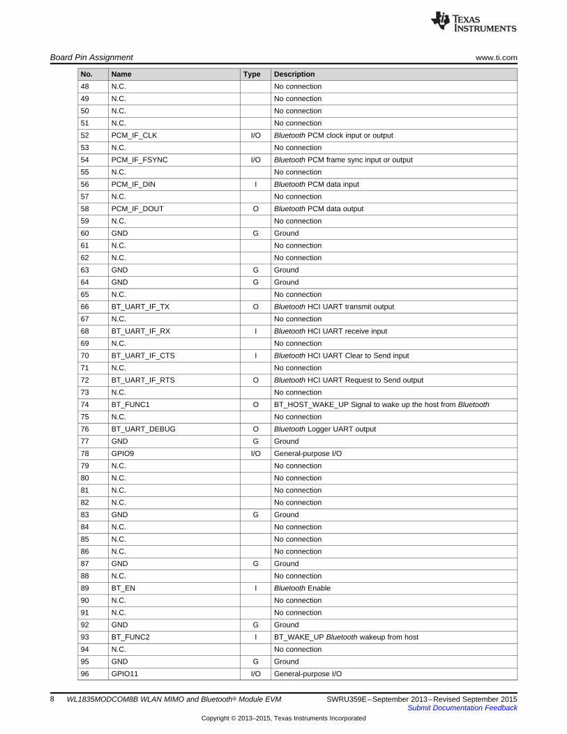
No. Name Type Description48 N.C. No connection49 N.C. No connection50 N.C. No connection51 N.C. No connection52 PCM_IF_CLK I/O Bluetooth PCM clock input or output53 N.C. No connection54 PCM_IF_FSYNC I/O Bluetooth PCM frame sync input or output55 N.C. No connection56 PCM_IF_DIN I Bluetooth PCM data input57 N.C. No connection58 PCM_IF_DOUT O Bluetooth PCM data output59 N.C. No connection60 GND G Ground61 N.C. No connection62 N.C. No connection63 GND G Ground64 GND G Ground65 N.C. No connection66 BT_UART_IF_TX O Bluetooth HCI UART transmit output67 N.C. No connection68 BT_UART_IF_RX I Bluetooth HCI UART receive input69 N.C. No connection70 BT_UART_IF_CTS I Bluetooth HCI UART Clear to Send input71 N.C. No connection72 BT_UART_IF_RTS O Bluetooth HCI UART Request to Send output73 N.C. No connection74 BT_FUNC1 O BT_HOST_WAKE_UP Signal to wake up the host from Bluetooth75 N.C. No connection76 BT_UART_DEBUG O Bluetooth Logger UART output77 GND G Ground78 GPIO9 I/O General-purpose I/O79 N.C. No connection80 N.C. No connection81 N.C. No connection82 N.C. No connection83 GND G Ground84 N.C. No connection85 N.C. No connection86 N.C. No connection87 GND G Ground88 N.C. No connection89 BT_EN I Bluetooth Enable90 N.C. No connection91 N.C. No connection92 GND G Ground93 BT_FUNC2 I BT_WAKE_UP Bluetooth wakeup from host94 N.C. No connection95 GND G Ground96 GPIO11 I/O General-purpose I/O
www.ti.com Electrical Characteristics
9SWRU359E–September 2013–Revised September 2015Submit Documentation Feedback
Copyright © 2013–2015, Texas Instruments Incorporated
WL1835MODCOM8B WLAN MIMO and Bluetooth® Module EVM
No. Name Type Description97 GND G Ground98 GPIO12 I/O General-purpose I/O99 N.C. General-purpose I/O100 GPIO10 I/O General-purpose I/O
4 Electrical CharacteristicsRefer to the detailed data in the WL18MODGB data sheet (SWRS152) for electrical characteristics.
5 Approved Antenna Types and Maximum Gain ValuesThis device is intended only for OEM integrators under the following conditions:• Install the antenna so that 20 cm is maintained between the antenna and user.• Do not co-locate the transmitter module with any other transmitter or antenna.• Operate the radio transmitter using only an antenna of a type and maximum (or lesser) gain approved
by TI. Table 1 lists the antennas approved by TI for use with the radio transmitter along with maximumallowable gain values. Antenna types not included in the list or having a gain greater than themaximum indicated are strictly prohibited for use with this transmitter
Table 1. Approved Antenna Types and Maximum Gain Values
Antenna Type Brand 2.4–2.5 GHz UnitPCB Ethertronics –0.600
dBi
Dipole LSR 2.00PCB Laird 2.00Chip Pulse 3.20PIFA LSR 2.00Chip TDK 2.4
NOTE: If these conditions cannot be met (for example, with certain laptop configurations or co-location with another transmitter), the FCC/IC authorization will not be considered valid andthe FCC ID/IC ID cannot be used on the final product. In these circumstances, the OEMintegrator is responsible for reevaluating the end product (including the transmitter) andobtaining a separate FCC/IC authorization.
On-Board Antenna Configuration www.ti.com
10 SWRU359E–September 2013–Revised September 2015Submit Documentation Feedback
Copyright © 2013–2015, Texas Instruments Incorporated
WL1835MODCOM8B WLAN MIMO and Bluetooth® Module EVM
6 On-Board Antenna Configuration
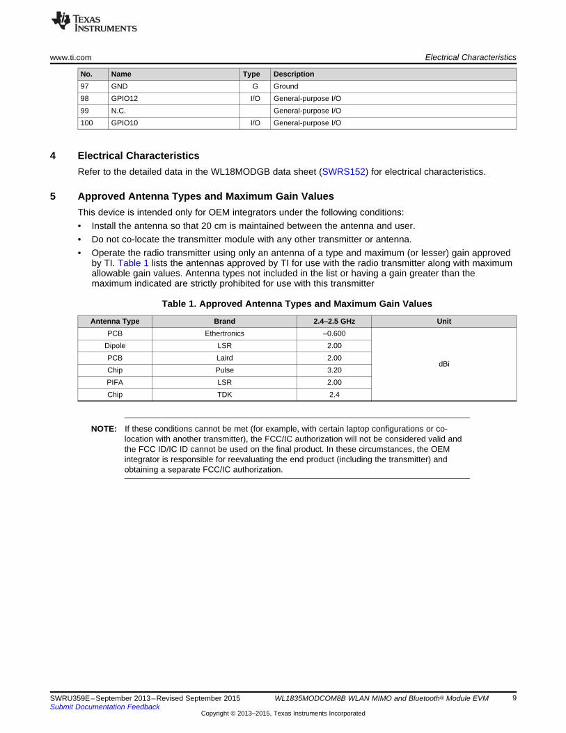
6.1 VSWRFigure 4 shows the antenna VSWR.
Figure 4. Antenna VSWR
www.ti.com On-Board Antenna Configuration
11SWRU359E–September 2013–Revised September 2015Submit Documentation Feedback
Copyright © 2013–2015, Texas Instruments Incorporated
WL1835MODCOM8B WLAN MIMO and Bluetooth® Module EVM
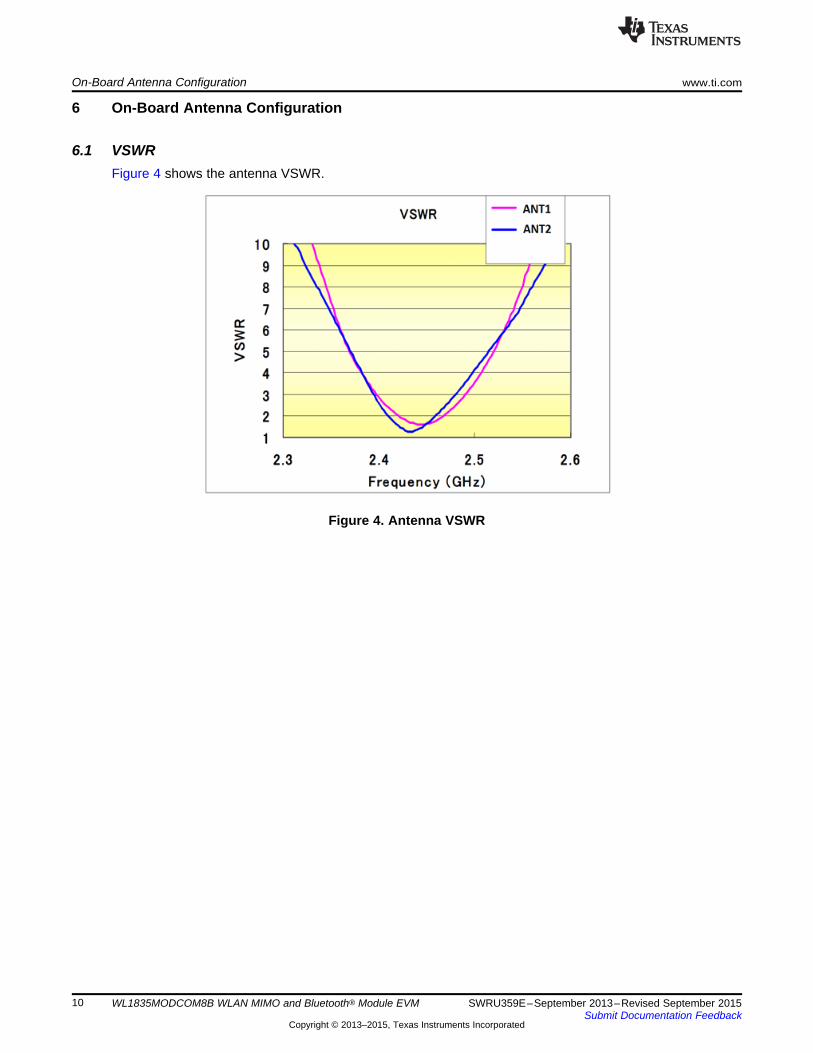
6.2 EfficiencyFigure 5 shows the antenna efficiency.
Figure 5. Antenna Efficiency
6.3 Radio PatternFigure 6 shows the radio pattern of the WL1835MODCOM8B device.
Figure 6. Radio Pattern
On-Board Antenna Configuration www.ti.com
12 SWRU359E–September 2013–Revised September 2015Submit Documentation Feedback
Copyright © 2013–2015, Texas Instruments Incorporated
WL1835MODCOM8B WLAN MIMO and Bluetooth® Module EVM
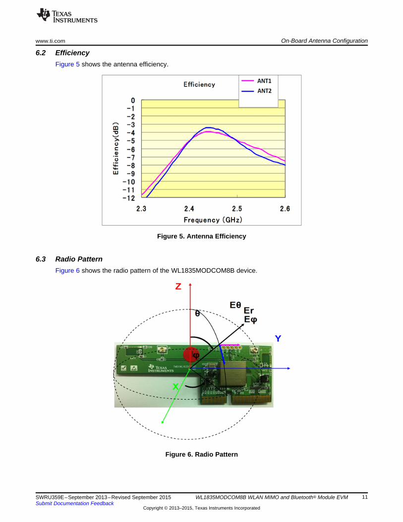
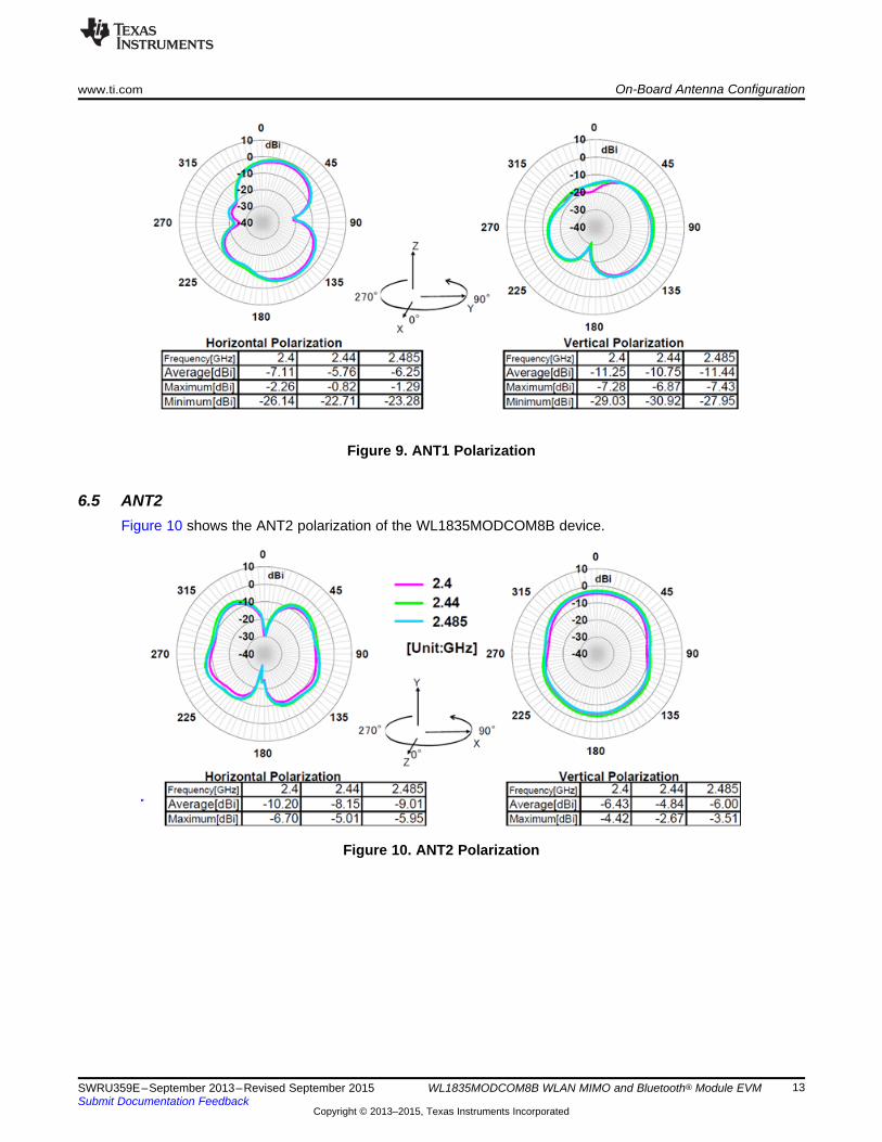
6.4 ANT1Figure 7 shows the ANT1 polarization of the WL1835MODCOM8B device.
Figure 7. ANT1 Polarization
Figure 8. ANT1 Polarization
www.ti.com On-Board Antenna Configuration
13SWRU359E–September 2013–Revised September 2015Submit Documentation Feedback
Copyright © 2013–2015, Texas Instruments Incorporated
WL1835MODCOM8B WLAN MIMO and Bluetooth® Module EVM
Figure 9. ANT1 Polarization
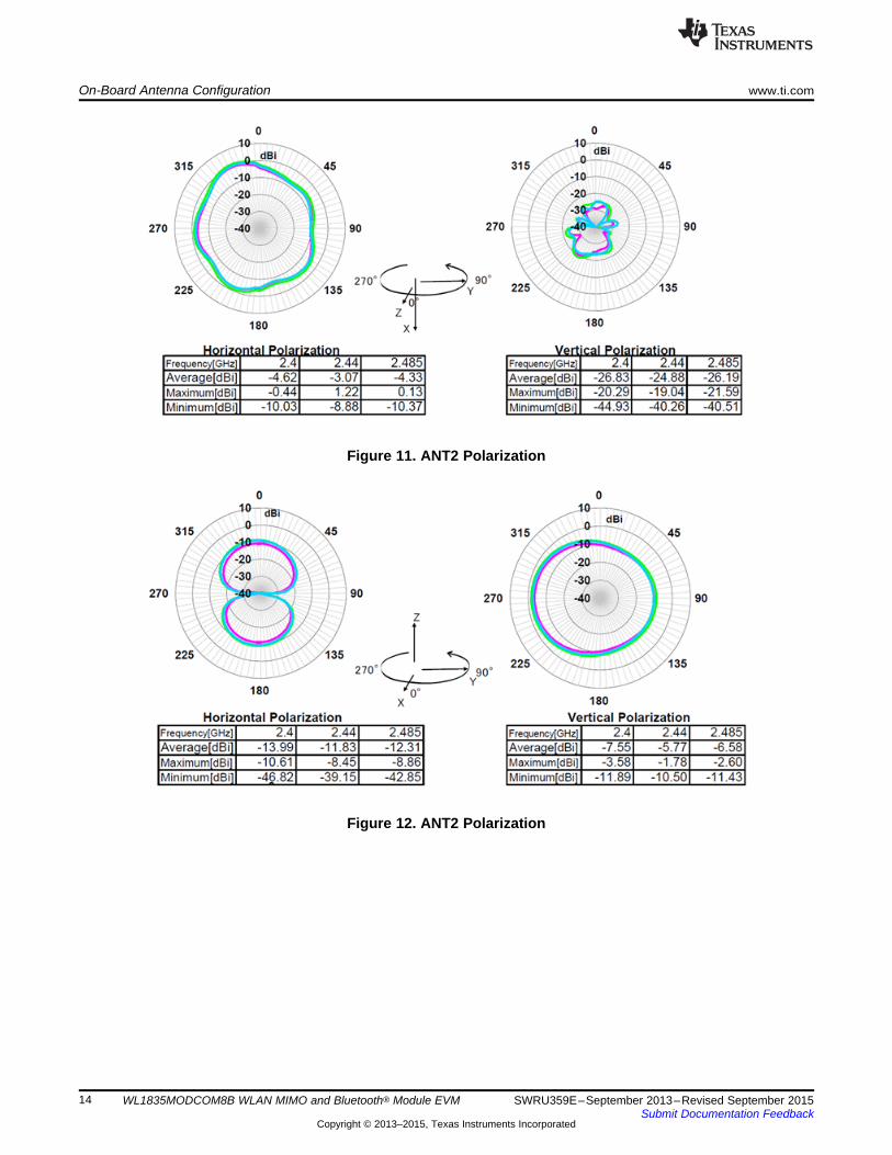
6.5 ANT2Figure 10 shows the ANT2 polarization of the WL1835MODCOM8B device.
Figure 10. ANT2 Polarization
On-Board Antenna Configuration www.ti.com
14 SWRU359E–September 2013–Revised September 2015Submit Documentation Feedback
Copyright © 2013–2015, Texas Instruments Incorporated
WL1835MODCOM8B WLAN MIMO and Bluetooth® Module EVM
Figure 11. ANT2 Polarization
Figure 12. ANT2 Polarization
EDGE CONNECTOR - MALE
WL_BG ANT2WL_BG/BT ANT1
Short PIN Header (1-2)for entering test mode.Open for function mode.
These two TPs for test modewhen WL_IRQ pull high.
WL_UART_DBG
BT_AUD_CLK
BT_AUD_FSYNC
BT_AUD_IN
WL_RS232_TX
WL_RS232_RX
BT_HCI_TX
BT_HCI_RX
BT_HCI_CTS
BT_HCI_RTS
BT_EN_SOC
BT_UART_DBG
SDIO_CLK_WL
SDIO_CMD_WL
SDIO_D0_WL
SDIO_D2_WL
SDIO_D3_WL
SDIO_D1_WL
WLAN_EN_SOC
BT_AUD_OUT
BT_FUNC1
GPIO9
GPIO11
GPIO12
GPIO10
SLOW_CLK
BT_FUNC2
WLAN_IRQ
2G4_ANT1_WB2G4_ANT2_W
SDIO_D3_WL
GPIO12
SDIO_D2_WL
GPIO11
SDIO_D0_WL
SDIO_D1_WL
GPIO9
WLAN_IRQ
GPIO10
2G4_ANT2_W
WL_RS232_TX
WL_RS232_RX
2G4_ANT1_WB
BT_FUNC1
BT_FUNC2
BT_HCI_RX
BT_HCI_TX
BT_HCI_CTS
BT_HCI_RTS
BT_AUD_IN
BT_AUD_OUT
BT_AUD_CLK
BT_AUD_FSYNC
SDIO_CMD_WL
SDIO_CLK_WL
SLOW_CLK
WL_UART_DBG
BT_UART_DBG
BT_EN_SOC
WLAN_EN_SOC
VBAT_IN
VIO_IN
VIO_IN
VBAT_IN
VIO_IN
VIO_IN
R20 10k0402
R25 0R 0402
C510pF0402
J6U.FL-R-SMT(10)U.FL
12
3
C144pF0402
ANT2ANT016008LCD2442MA1ANT-N3-1.6X0.8MM-B
5G
B2
FEEDA
2.4G
B1
R17 0R 0402
C610pF0402
J2NU_100pin Micro Edge MEC6SD-100P
1 2
3 4
5 6
7 8
9 10
11 12
13 14
15 16
17 18
19 20
21 22
23 24
25 26
27 28
29 30
31 32
33 34
35 36
37 38
39 40
41 42
43 44
45 46
47 48
49 50
51 52
53 54
55 56
57 58
59 60
61 62
63 64
65 66
67 68
69 70
71 72
73 74
75 76
77 78
79 80
81 82
83 84
85 86
87 88
89 90
91 92
93 94
95 96
97 98
99 100
TP41
C7NU_10pF0402 C9
2pF0402
R12 0R 0402
C111.2pF0402
R11 0R 0402
ANT1ANT016008LCD2442MA1ANT-N3-1.6X0.8MM-A
5G
B2
FEEDA
2.4G
B1
C11uF0402
R30 0R 0402
R9 0R 0402
J5U.FL-R-SMT(10)U.FL
12
3
C10NU_0.3pF0402
R10 0R0402
TP1 1
TP51
R2 0R 0402
0RR21 0402
TP6 1
0RR19 0402
OSC11V8 / 32.768kHzOSC-3.2X2.5
EN1
VCC4
OUT3
GND2
R60R0402
R3 0R 0402
R16 0R 0402
U1
WL1835MODGB
E-13.4X13.3-N100_0.75-TOP
GP
IO9
3
GP
IO12
5
GP
IO11
2
GP
IO10
4
GND17
VIO
38
VB
AT
47
EX
T_32K
36
BT_AUD_FSYNC58
BT_AUD_IN56
BT_AUD_OUT57
BT_AUD_CLK60
WL_S
DIO
_D
212
WL_S
DIO
_C
LK
8
WL_S
DIO
_D
313
WL_S
DIO
_D
010
WL_S
DIO
_D
111
WL_S
DIO
_C
MD
6
BT_HCI_RTS50
BT_HCI_RX53
BT_HCI_TX52
BT_HCI_CTS51
GN
D16
GPIO_425
GPIO_226
GPIO_127
BT
_E
N_S
OC
41
WLA
N_IR
Q14
WLA
N_E
N_S
OC
40
BT
_U
AR
T_D
BG
43
WL_U
AR
T_D
BG
42
GNDG13
GNDG14
GNDG15
GNDG16
GNDG9
GNDG10
GN
D48
GNDG11
GNDG12
VB
AT
46
GND28
GNDG1
GNDG2
GNDG3
GNDG4
GNDG5
GNDG6
GNDG7
GNDG8
2G4_ANT1_WB32
GND64
GN
D1
GND20
RESERVED121
RESERVED222
GN
D37
GND19
RESERVED362
GNDG17
GNDG18
GNDG19
GNDG20
GNDG21
GNDG22
GNDG23
GNDG24
GNDG25
GNDG26
GNDG27
GNDG28
GNDG29
GNDG30
GNDG31
GNDG32
GNDG33
GNDG34
GNDG35
GND23
GND59
GN
D34
GND29
GN
D7
2G4_ANT2_W18
GND49
GN
D9
GND31
GN
D35
GN
D15
GND55
GN
D45
GN
D44
GND30
GND24
GND63
GND61
GN
D39
GN
D33
GND54
GNDG36
C210uF0603
R310R0402
J1HEADER 1x2H-1X2_2MM
12
R1 0R 0402
R29 0R 0402
R8 0R 0402
L1
04021.1nH
TP31
R28 0R 0402
0RR24 0402
R7 0R 0402
TP8 1
R14 0R 0402
C8NU_10pF0402
C40.1uF0402
R27 0R 0402
R13 0R 0402
R15 0R 0402
C30.1uF0402
0RR22 0402
R18 0R 0402
R4 0R 0402
R23 0R 0402
R320R0402
C138pF0402
R5 NU_0R0402
C12NU0402
J3HEADER 1x2H-1X2_2MM
12
J4HEADER 1x2H-1X2_2MM
1 2
0RR26 0402
L21.5nH0402
TP2 1
www.ti.com Circuit Design
15SWRU359E–September 2013–Revised September 2015Submit Documentation Feedback
Copyright © 2013–2015, Texas Instruments Incorporated
WL1835MODCOM8B WLAN MIMO and Bluetooth® Module EVM
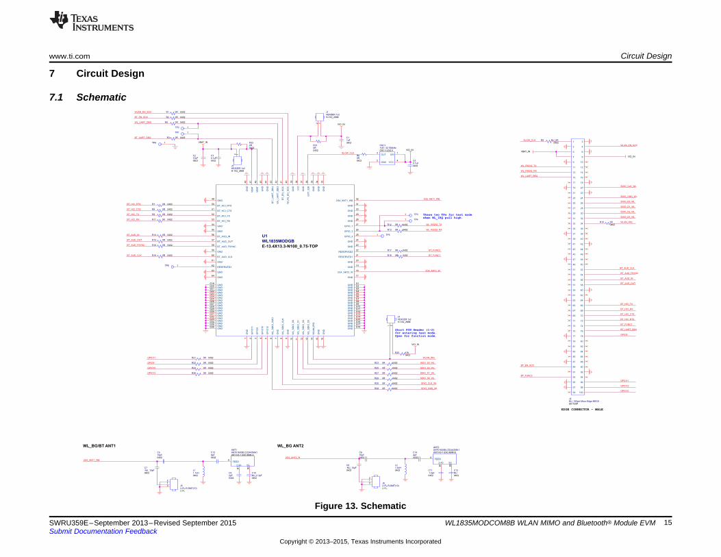
7 Circuit Design
7.1 Schematic
Figure 13. Schematic
Circuit Design www.ti.com
16 SWRU359E–September 2013–Revised September 2015Submit Documentation Feedback
Copyright © 2013–2015, Texas Instruments Incorporated
WL1835MODCOM8B WLAN MIMO and Bluetooth® Module EVM
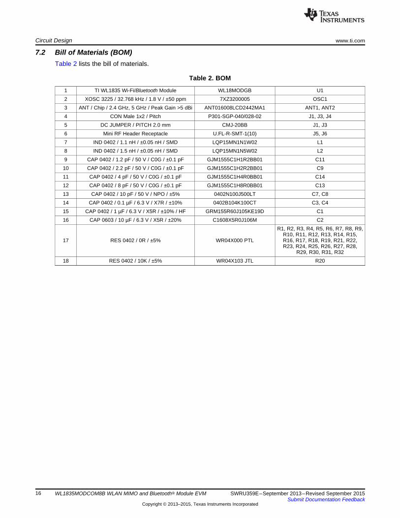
7.2 Bill of Materials (BOM)Table 2 lists the bill of materials.
Table 2. BOM
1 TI WL1835 Wi-Fi/Bluetooth Module WL18MODGB U12 XOSC 3225 / 32.768 kHz / 1.8 V / ±50 ppm 7XZ3200005 OSC13 ANT / Chip / 2.4 GHz, 5 GHz / Peak Gain >5 dBi ANT016008LCD2442MA1 ANT1, ANT24 CON Male 1x2 / Pitch P301-SGP-040/028-02 J1, J3, J45 DC JUMPER / PITCH 2.0 mm CMJ-20BB J1, J36 Mini RF Header Receptacle U.FL-R-SMT-1(10) J5, J67 IND 0402 / 1.1 nH / ±0.05 nH / SMD LQP15MN1N1W02 L18 IND 0402 / 1.5 nH / ±0.05 nH / SMD LQP15MN1N5W02 L29 CAP 0402 / 1.2 pF / 50 V / C0G / ±0.1 pF GJM1555C1H1R2BB01 C1110 CAP 0402 / 2.2 pF / 50 V / C0G / ±0.1 pF GJM1555C1H2R2BB01 C911 CAP 0402 / 4 pF / 50 V / C0G / ±0.1 pF GJM1555C1H4R0BB01 C1412 CAP 0402 / 8 pF / 50 V / C0G / ±0.1 pF GJM1555C1H8R0BB01 C1313 CAP 0402 / 10 pF / 50 V / NPO / ±5% 0402N100J500LT C7, C814 CAP 0402 / 0.1 µF / 6.3 V / X7R / ±10% 0402B104K100CT C3, C415 CAP 0402 / 1 µF / 6.3 V / X5R / ±10% / HF GRM155R60J105KE19D C116 CAP 0603 / 10 µF / 6.3 V / X5R / ±20% C1608X5R0J106M C2
17 RES 0402 / 0R / ±5% WR04X000 PTL
R1, R2, R3, R4, R5, R6, R7, R8, R9,R10, R11, R12, R13, R14, R15,R16, R17, R18, R19, R21, R22,R23, R24, R25, R26, R27, R28,
R29, R30, R31, R3218 RES 0402 / 10K / ±5% WR04X103 JTL R20
www.ti.com Layout Guidelines
17SWRU359E–September 2013–Revised September 2015Submit Documentation Feedback
Copyright © 2013–2015, Texas Instruments Incorporated
WL1835MODCOM8B WLAN MIMO and Bluetooth® Module EVM
8 Layout Guidelines
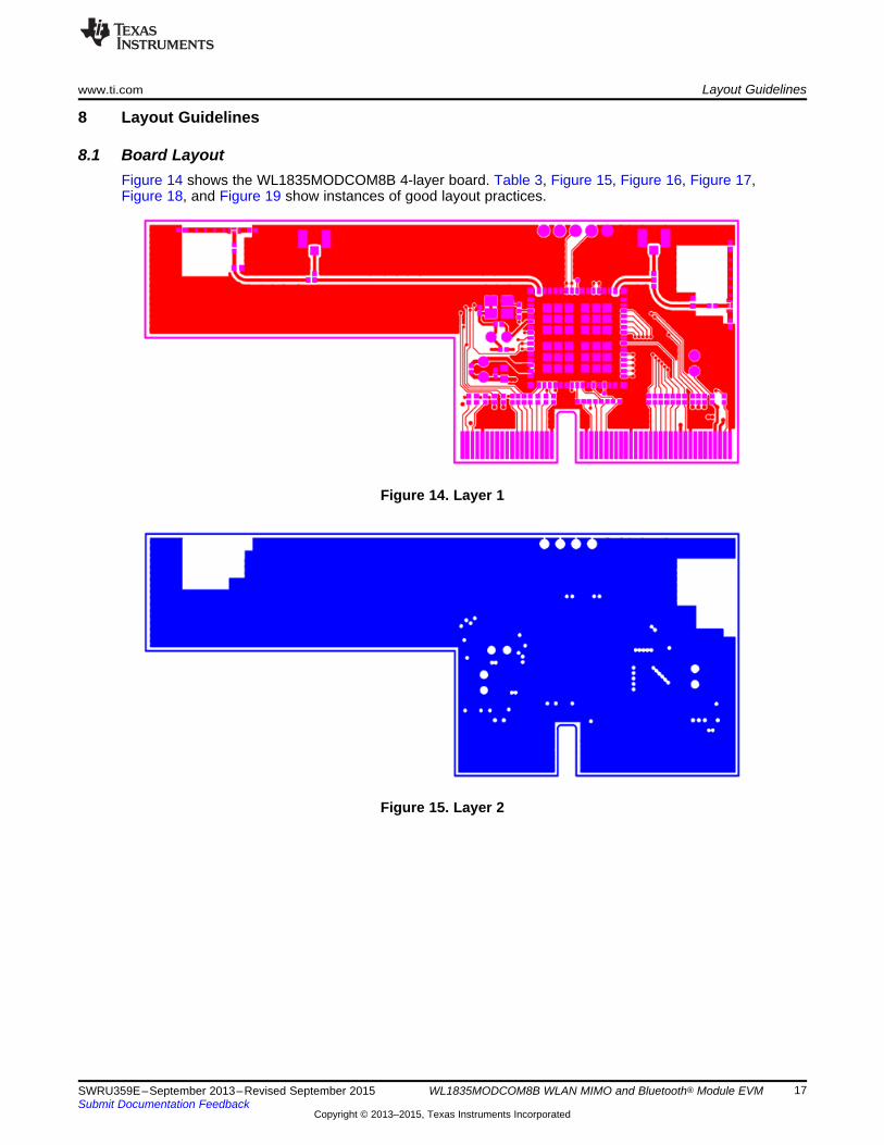
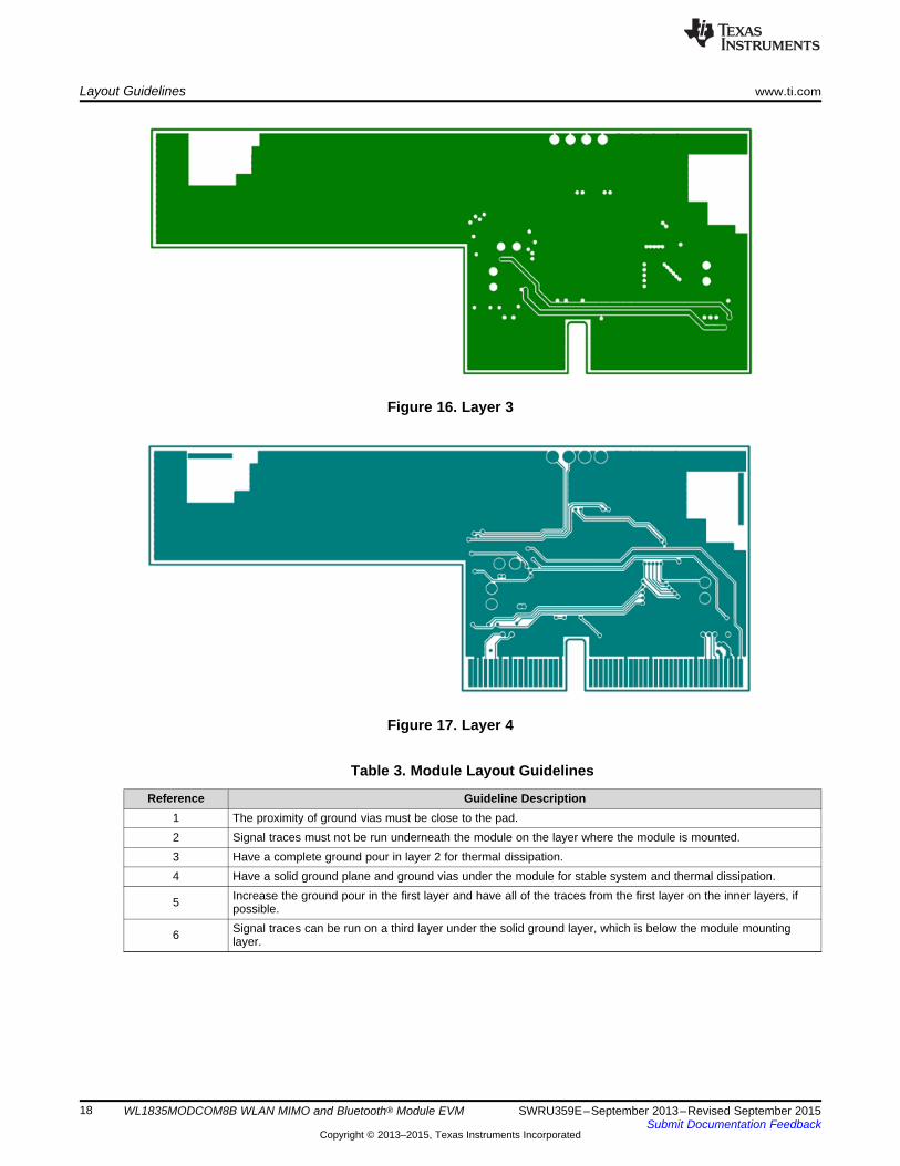
8.1 Board LayoutFigure 14 shows the WL1835MODCOM8B 4-layer board. Table 3, Figure 15, Figure 16, Figure 17,Figure 18, and Figure 19 show instances of good layout practices.
Figure 14. Layer 1
Figure 15. Layer 2
Layout Guidelines www.ti.com
18 SWRU359E–September 2013–Revised September 2015Submit Documentation Feedback
Copyright © 2013–2015, Texas Instruments Incorporated
WL1835MODCOM8B WLAN MIMO and Bluetooth® Module EVM
Figure 16. Layer 3
Figure 17. Layer 4
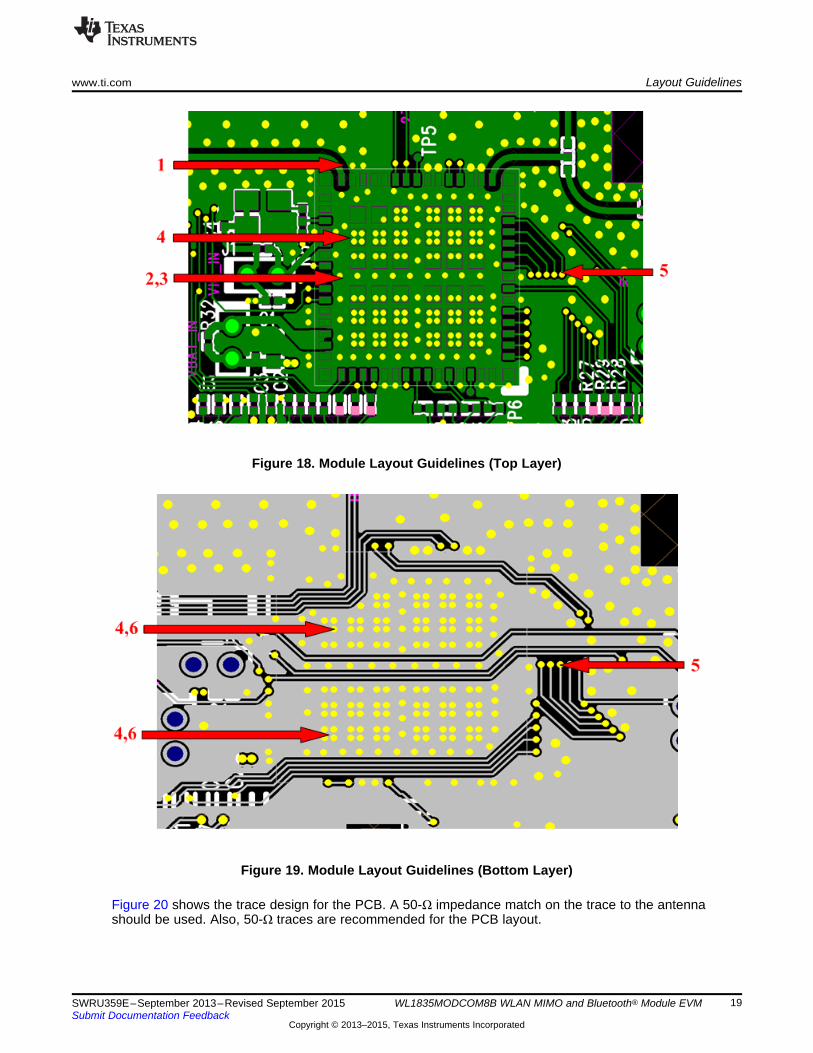
Table 3. Module Layout Guidelines
Reference Guideline Description1 The proximity of ground vias must be close to the pad.2 Signal traces must not be run underneath the module on the layer where the module is mounted.3 Have a complete ground pour in layer 2 for thermal dissipation.4 Have a solid ground plane and ground vias under the module for stable system and thermal dissipation.
5 Increase the ground pour in the first layer and have all of the traces from the first layer on the inner layers, ifpossible.
6 Signal traces can be run on a third layer under the solid ground layer, which is below the module mountinglayer.
www.ti.com Layout Guidelines
19SWRU359E–September 2013–Revised September 2015Submit Documentation Feedback
Copyright © 2013–2015, Texas Instruments Incorporated
WL1835MODCOM8B WLAN MIMO and Bluetooth® Module EVM
Figure 18. Module Layout Guidelines (Top Layer)
Figure 19. Module Layout Guidelines (Bottom Layer)
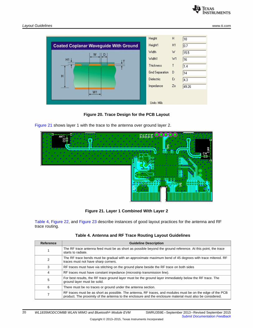
Figure 20 shows the trace design for the PCB. A 50-Ω impedance match on the trace to the antennashould be used. Also, 50-Ω traces are recommended for the PCB layout.
Layout Guidelines www.ti.com
20 SWRU359E–September 2013–Revised September 2015Submit Documentation Feedback
Copyright © 2013–2015, Texas Instruments Incorporated
WL1835MODCOM8B WLAN MIMO and Bluetooth® Module EVM
Figure 20. Trace Design for the PCB Layout
Figure 21 shows layer 1 with the trace to the antenna over ground layer 2.
Figure 21. Layer 1 Combined With Layer 2
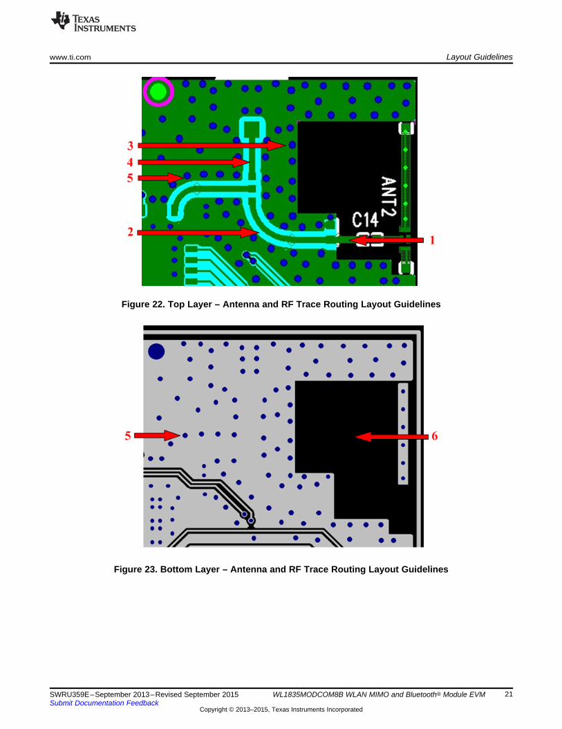
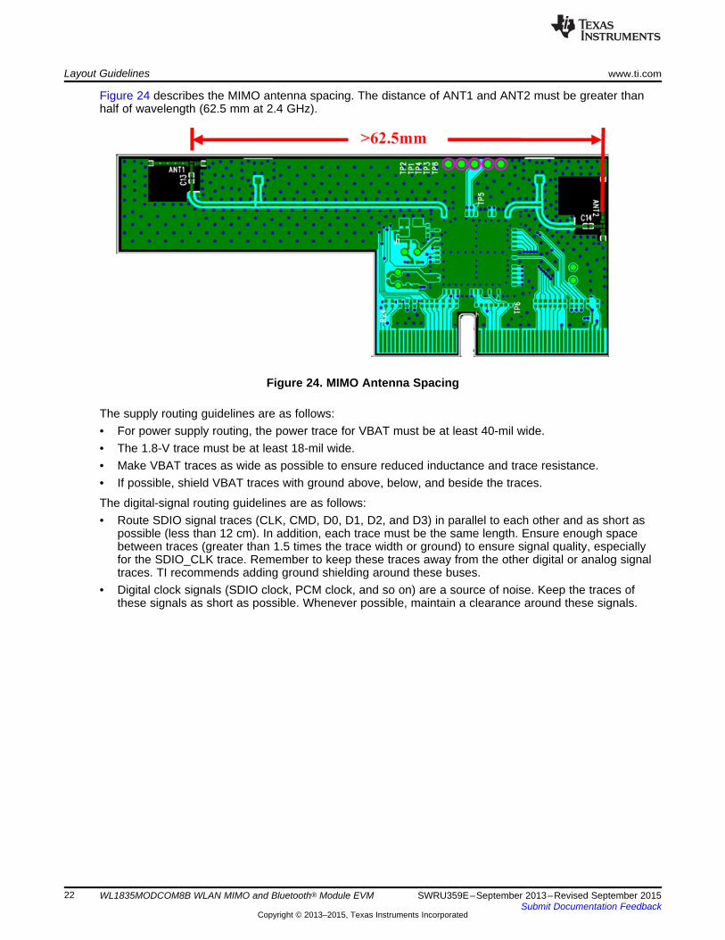
Table 4, Figure 22, and Figure 23 describe instances of good layout practices for the antenna and RFtrace routing.
Table 4. Antenna and RF Trace Routing Layout Guidelines
Reference Guideline Description
1 The RF trace antenna feed must be as short as possible beyond the ground reference. At this point, the tracestarts to radiate.
2 The RF trace bends must be gradual with an approximate maximum bend of 45 degrees with trace mitered. RFtraces must not have sharp corners.
3 RF traces must have via stitching on the ground plane beside the RF trace on both sides4 RF traces must have constant impedance (microstrip transmission line).
5 For best results, the RF trace ground layer must be the ground layer immediately below the RF trace. Theground layer must be solid.
6 There must be no traces or ground under the antenna section.
7 RF traces must be as short as possible. The antenna, RF traces, and modules must be on the edge of the PCBproduct. The proximity of the antenna to the enclosure and the enclosure material must also be considered.
www.ti.com Layout Guidelines
21SWRU359E–September 2013–Revised September 2015Submit Documentation Feedback
Copyright © 2013–2015, Texas Instruments Incorporated
WL1835MODCOM8B WLAN MIMO and Bluetooth® Module EVM
Figure 22. Top Layer – Antenna and RF Trace Routing Layout Guidelines
Figure 23. Bottom Layer – Antenna and RF Trace Routing Layout Guidelines
Layout Guidelines www.ti.com
22 SWRU359E–September 2013–Revised September 2015Submit Documentation Feedback
Copyright © 2013–2015, Texas Instruments Incorporated
WL1835MODCOM8B WLAN MIMO and Bluetooth® Module EVM
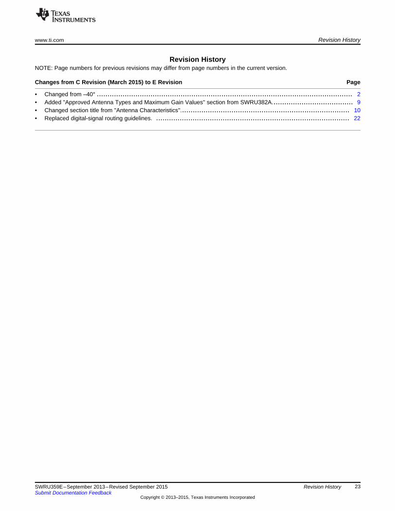
Figure 24 describes the MIMO antenna spacing. The distance of ANT1 and ANT2 must be greater thanhalf of wavelength (62.5 mm at 2.4 GHz).
Figure 24. MIMO Antenna Spacing
The supply routing guidelines are as follows:• For power supply routing, the power trace for VBAT must be at least 40-mil wide.• The 1.8-V trace must be at least 18-mil wide.• Make VBAT traces as wide as possible to ensure reduced inductance and trace resistance.• If possible, shield VBAT traces with ground above, below, and beside the traces.
The digital-signal routing guidelines are as follows:• Route SDIO signal traces (CLK, CMD, D0, D1, D2, and D3) in parallel to each other and as short as
possible (less than 12 cm). In addition, each trace must be the same length. Ensure enough spacebetween traces (greater than 1.5 times the trace width or ground) to ensure signal quality, especiallyfor the SDIO_CLK trace. Remember to keep these traces away from the other digital or analog signaltraces. TI recommends adding ground shielding around these buses.
• Digital clock signals (SDIO clock, PCM clock, and so on) are a source of noise. Keep the traces ofthese signals as short as possible. Whenever possible, maintain a clearance around these signals.
www.ti.com Revision History
23SWRU359E–September 2013–Revised September 2015Submit Documentation Feedback
Copyright © 2013–2015, Texas Instruments Incorporated
Revision History
Revision HistoryNOTE: Page numbers for previous revisions may differ from page numbers in the current version.
Changes from C Revision (March 2015) to E Revision .................................................................................................. Page
• Changed from –40° ....................................................................................................................... 2• Added "Approved Antenna Types and Maximum Gain Values" section from SWRU382A...................................... 9• Changed section title from "Antenna Characteristics"............................................................................... 10• Replaced digital-signal routing guidelines. .......................................................................................... 22
IMPORTANT NOTICE FOR TI DESIGN INFORMATION AND RESOURCES
Texas Instruments Incorporated (‘TI”) technical, application or other design advice, services or information, including, but not limited to,reference designs and materials relating to evaluation modules, (collectively, “TI Resources”) are intended to assist designers who aredeveloping applications that incorporate TI products; by downloading, accessing or using any particular TI Resource in any way, you(individually or, if you are acting on behalf of a company, your company) agree to use it solely for this purpose and subject to the terms ofthis Notice.TI’s provision of TI Resources does not expand or otherwise alter TI’s applicable published warranties or warranty disclaimers for TIproducts, and no additional obligations or liabilities arise from TI providing such TI Resources. TI reserves the right to make corrections,enhancements, improvements and other changes to its TI Resources.You understand and agree that you remain responsible for using your independent analysis, evaluation and judgment in designing yourapplications and that you have full and exclusive responsibility to assure the safety of your applications and compliance of your applications(and of all TI products used in or for your applications) with all applicable regulations, laws and other applicable requirements. Yourepresent that, with respect to your applications, you have all the necessary expertise to create and implement safeguards that (1)anticipate dangerous consequences of failures, (2) monitor failures and their consequences, and (3) lessen the likelihood of failures thatmight cause harm and take appropriate actions. You agree that prior to using or distributing any applications that include TI products, youwill thoroughly test such applications and the functionality of such TI products as used in such applications. TI has not conducted anytesting other than that specifically described in the published documentation for a particular TI Resource.You are authorized to use, copy and modify any individual TI Resource only in connection with the development of applications that includethe TI product(s) identified in such TI Resource. NO OTHER LICENSE, EXPRESS OR IMPLIED, BY ESTOPPEL OR OTHERWISE TOANY OTHER TI INTELLECTUAL PROPERTY RIGHT, AND NO LICENSE TO ANY TECHNOLOGY OR INTELLECTUAL PROPERTYRIGHT OF TI OR ANY THIRD PARTY IS GRANTED HEREIN, including but not limited to any patent right, copyright, mask work right, orother intellectual property right relating to any combination, machine, or process in which TI products or services are used. Informationregarding or referencing third-party products or services does not constitute a license to use such products or services, or a warranty orendorsement thereof. Use of TI Resources may require a license from a third party under the patents or other intellectual property of thethird party, or a license from TI under the patents or other intellectual property of TI.TI RESOURCES ARE PROVIDED “AS IS” AND WITH ALL FAULTS. TI DISCLAIMS ALL OTHER WARRANTIES ORREPRESENTATIONS, EXPRESS OR IMPLIED, REGARDING TI RESOURCES OR USE THEREOF, INCLUDING BUT NOT LIMITED TOACCURACY OR COMPLETENESS, TITLE, ANY EPIDEMIC FAILURE WARRANTY AND ANY IMPLIED WARRANTIES OFMERCHANTABILITY, FITNESS FOR A PARTICULAR PURPOSE, AND NON-INFRINGEMENT OF ANY THIRD PARTY INTELLECTUALPROPERTY RIGHTS.TI SHALL NOT BE LIABLE FOR AND SHALL NOT DEFEND OR INDEMNIFY YOU AGAINST ANY CLAIM, INCLUDING BUT NOTLIMITED TO ANY INFRINGEMENT CLAIM THAT RELATES TO OR IS BASED ON ANY COMBINATION OF PRODUCTS EVEN IFDESCRIBED IN TI RESOURCES OR OTHERWISE. IN NO EVENT SHALL TI BE LIABLE FOR ANY ACTUAL, DIRECT, SPECIAL,COLLATERAL, INDIRECT, PUNITIVE, INCIDENTAL, CONSEQUENTIAL OR EXEMPLARY DAMAGES IN CONNECTION WITH ORARISING OUT OF TI RESOURCES OR USE THEREOF, AND REGARDLESS OF WHETHER TI HAS BEEN ADVISED OF THEPOSSIBILITY OF SUCH DAMAGES.You agree to fully indemnify TI and its representatives against any damages, costs, losses, and/or liabilities arising out of your non-compliance with the terms and provisions of this Notice.This Notice applies to TI Resources. Additional terms apply to the use and purchase of certain types of materials, TI products and services.These include; without limitation, TI’s standard terms for semiconductor products http://www.ti.com/sc/docs/stdterms.htm), evaluationmodules, and samples (http://www.ti.com/sc/docs/sampterms.htm).
Mailing Address: Texas Instruments, Post Office Box 655303, Dallas, Texas 75265Copyright © 2018, Texas Instruments Incorporated


