Universidade de Lisboa
Faculdade de Ciências
(Departamento de Física)
Development of a Rapid Prototyping method for Hard Polymer Microfluidic
Systems tested through iterative design of a PCR chamber chip
Miguel Barreiros
Dissertação
Mestrado Integrado em Engenharia Biomédica e Biofísica
Perfil em Engenharia Clínica e Instrumentação Médica
2014

2
Universidade de Lisboa
Faculdade de Ciências
Departamento de Física
Development of a Rapid Prototyping method for Hard Polymer Microfluidic
Systems tested through iterative design of a PCR chamber chip
Miguel Barreiros
Dissertação
Mestrado Integrado em Engenharia Biomédica e Biofísica
Perfil em Engenharia Clínica e Instrumentação Médica
Orientadores: Dr. Hugo Ferreira
Samuel K. Sia, PhD

3
Abstract
One of the challenges of working with polymer microfluidics is the lack of an established
prototyping method which allows for easy translation to industrial production. By combining Hot
Embossing and Computer Numerically Controlled Milling a microfluidic rapid prototyping method
was established for Polycarbonate and Cyclic Olefin Polymer. This method was then tested and
optimized through an iterative design process of a microfluidic Polymerase-Chain Reaction
chamber. The fabrication method proved to be suitable for microfluidic prototyping, allowing for
rapid design changes and fabrication of good quality copies in a simple and straightforward fashion.
Keywords: Microfluidics, Hot Embossing, Rapid Prototyping, Hard Polymers, Fabrication, PCR

4
Resumo
Uma das dificuldades em trabalhar com microfluídica em polímeros é a falta da existência
de um método de prototipagem que permita uma passagem simples para um ambiente de produção
industrial. Neste trabalho foi desenvolvido um método de prototipagem rápida para microfluídica
em Policarbonato e Cyclic Olefin Polymer utilizando uma Fresadora de Controlo Numérico
Computorizado e Hot Embossing. Este método foi testado e optimizado através de um processo de
design iterativo de uma câmara microfluídica de Reacção em Cadeia da Polimerase em
Policarbonato. O método desenvolvido provou ser adequado para prototipagem microfluídica,
permitindo alterações rápidas ao desenho e fabricação de várias cópias com boa qualidade de cada
desenho.
Palavras-chave: Microfluídica, Hot Embossing, Estampagem a Quente, Prototipagem Rápida,
Polímeros Duros, Fabricação, PCR

5
Contents 1. Motivation .......................................................................................................................... 9
2. Microfluidic Fabrication ................................................................................................... 11
2.1. Brief History of Microfluidics..................................................................................... 11
2.2. Micro vs Macro .......................................................................................................... 13
2.3. Fabrication methods ................................................................................................. 16
2.3.1. Soft Lithography ................................................................................................. 16
2.3.2. Micro Injection molding ..................................................................................... 19
2.3.3. Hot embossing.................................................................................................... 21
2.4. Mold Fabrication ....................................................................................................... 25
3. PCR ................................................................................................................................... 31
3.1. Miniaturization of PCR .............................................................................................. 32
4. Methodology .................................................................................................................... 34
4.1. Materials ................................................................................................................... 37
5. Results and Discussion ..................................................................................................... 39
5.1 Testing Hot Embossing protocols and mold fabrication methods ............................. 39
5.2 Development of a hard polymer PCR chip ................................................................. 43
5.2.3. PCR experiments ................................................................................................ 46
6. Conclusion ........................................................................................................................ 55
7. Bibliography ..................................................................................................................... 56
8. Annex................................................................................................................................ 62
a) Arduino code for temperature control and thermocycling protocol ........................... 62
b) Excerpt of G-Code ........................................................................................................ 65

6
List of Figures
FIGURE 1: EXAMPLE OF LAMINAR FLOW IN A MICROFLUIDIC SYSTEM. 14
FIGURE 2: DIAGRAM OF THE SL MASTER FABRICATION STEPS. 17
FIGURE 3: DIAGRAM OF THE SL PDMS CASTING STEPS. 18
FIGURE 4: DIAGRAM OF AN INJECTION MOLDING CYCLE. 19
FIGURE 5 DIAGRAM OF A HOT EMBOSSING CYCLE. 22
FIGURE 6: PRESSURE AND TEMPERATURE DIAGRAM OF A HOT EMBOSSING CYCLE. 23
FIGURE 7: BROKEN SI WAFER WITH SU-8 FEATURES. 26
FIGURE 8: CNC MILLING APPARATUS. 28
FIGURE 9: DIFFERENT MILLING TYPES. 29
FIGURE 10: MICROPHOTOGRAPH OF A MICRO END-MILL WITH 200 ΜM DIAMETER. 30
FIGURE 11: DIAGRAM OF A 3-STEP PCR THERMOCYCLING PROTOCOL. 31
FIGURE 12: SCHEMATIC ILLUSTRATIONS OF TYPES OF MICROFLUIDIC PCR CHIP DESIGNS 33
FIGURE 13: HOT EMBOSSING EQUIPMENT 39
FIGURE 14: PIECES OF A BROKEN SU-8/SILICON MOLD. 40
FIGURE 15: CROSS-SECTIONS OF THE MILLED CHANNELS OBTAINED THROUGH PDMS CASTING. 41
FIGURE 16 : EMBOSSED PC CHIP. 41
FIGURE 17: MEANDERING CHANNELS 120 ΜM WIDE. 42
FIGURE 18: PCR CHIP WITH FEATURES DIRECTLY MILLED ON THE PC SUBSTRATE 43
FIGURE 19: FIRST MOLD DESIGN 44
FIGURE 20: DIAGRAM OF EMBOSSING SETUP. 45
FIGURE 21: PCR AMPLIFICATION RESULTS OBTAINED THROUGH GEL ELECTROPHORESIS. 46
FIGURE 22: TWO PART MOLD. 47
FIGURE 23: TWO CHAMBER DESIGN. 48
FIGURE 24: SINGLE CHAMBER DESIGN. 49
FIGURE 25: INTEGRATION OF A THERMOCOUPLE IN THE REACTION CHAMBER. 50
FIGURE 26: SECOND SINGLE CHAMBER DESIGN. 51
FIGURE 27: THERMOCYCLING SETUP WITH THE TEMPERATURE CONTROL CIRCUIT 52
FIGURE 28: TEMPERATURE PROFILE OF BOTH THERMOCOUPLES DURING THERMOCYCLING. 53
FIGURE 29: BUBBLE FORMATION DURING THERMOCYCLING. 54

7
List of Tables
TABLE 1: SUMMARY OF THE VARIOUS FABRICATION METHODS. 24

8
List of Used Acronyms
CAD Computer-Aided Drawing
CAM Computer-Aided Manufacturing
CF-PCR Continuous Flow Polymerase-Chain Reaction
CNC Computer Numerical Control
COP Cyclic Olefin Polymer
DOC Depth of Cut
HE Hot Embossing
IM Injection Molding
IPA Isopropyl alcohol
MEMS Microelectromechanical systems
PC Polycarbonate
PCR Polymerase-Chain Reaction
PDMS Polydimethylsiloxane
POC Point-of-Care
RPM Rotations per minute
SL Soft Lithography
SW SolidWorks
UHSM Ultra High Speed Machining
9
1. Motivation
Microfluidics as a research field has seen exponential growth in the last decades.
Unfortunately, there have been few truly successful products reaching the market. This gap is mostly
due to the difference in fabrication methods between research and production settings. There is a
need for a rapid prototyping method that allows for simple translation from a prototyping
environment to a cost-efficient industrial fabrication one. For many microfluidic applications the
chips need to be durable, disposable and inexpensive. This has been accomplished by fabricating
the chips in hard plastic through Injection Molding (IM) as this method is very cost-efficient for large-
scale fabrication. IM however does not allow for rapid prototyping as each design change requires
extensive optimization.
With that in mind, a rapid prototyping method for hard plastic microfluidics was developed
using Hot Embossing (HE). HE allows the fabrication of hard plastic microfluidic structures without
extensive optimization and is a good candidate for rapid prototyping when combined with a fast
mold fabrication method. Most of the previous work on HE has been done using labor-intensive
molds and is not applicable to a rapid prototyping scenario. The choice of mold fabrication method
will determine the cost and time necessary to fabricate a chip with a new design. In this work
Computer Numerical Controlled (CNC) milling was chosen because it is an extremely versatile
technology which has previously been used to mill micro structures in metal substrates.
This method was tested and optimized in the development of a microfluidic Polymerase-
Chain Reaction (PCR) chip through iterative design. The development of a PCR chip is a non-trivial
challenge and it was necessary that the fabrication method could produce different designs fast and
cheaply so as to quickly identify and correct problems along the design process. This allowed testing
the suitability of the fabrication method in a research setting.
In the first part of this work a small introduction to microfluidics and microfluidic fabrication
is presented, with added emphasis on HE and Mold Fabrication. A brief introduction to PCR
miniaturization is presented to better understand the potential of a microfluidic PCR chip and the
challenges associated with its development.

10
In the next section a description of the experimental methods is presented followed by the
results obtained using the fabrication method developed to iterate on a PCR chip design. The
experimental work began with testing different hot embossing protocols and mold fabrication
methods. For the following work, CNC milling was chosen as the mold fabrication method due to
the durability of the molds and the versatility of the technique. The PCR chip development began
with the adaption of an existing design which was iterated as needed. During the iterative design
process the fabrication method was continually optimized to obtain a more robust protocol.

11
2. Microfluidic Fabrication
This section begins with a small introduction to microfluidics and the history of the field to
help understand the state-of-the-art and the influence of the different fabrication methods in the
systems developed. The physical characteristics of micro-scale systems are then briefly analyzed to
better understand the possibilities and limitations of a microfluidic device.
The most relevant microfluidic fabrication methods are then described in detail and
compared in terms of their limitations and applicability to rapid prototyping. Mold fabrication
methods are also highlighted as they are critical in a rapid prototyping scenario.
Afterwards, a brief introduction to PCR amplification and the miniaturization of the process
are given so that the design goals are well understood.
2.1. Brief History of Microfluidics
Microfluidics as a field began in the 1990’s, based on the knowledge acquired developing
microelectromechanical systems (MEMS) which themselves were based on knowledge developed
on the miniaturization of electronic devices. During the 1970’s the miniaturization of electronics
produced different silicon technologies such as dry and wet etching or photolithography, which also
allowed the machining of miniaturized mechanical devices. These consisted mostly of physical
sensors (pressure, acceleration, etc) combined with integrated electronic circuits [1].
MEMS continued to be developed, with several commercial applications reaching the
market - inkjet printer cartridges and digital micromirror devices (DMD) for DLP projectors, for
example. In the late 1980’s several MEMS capable of fluid control were developed – microflow
sensors, micropumps, microvalves – and this marked the start of the microfluidics field. After the
reviews by Manz et al, in 1990 [2], presenting the biomedical applications of microfluidic systems,
the field grew rapidly with intensive research focused in miniaturizing chemical processes. The main
goal was to take advantage of the effects of the small-scale in fluid behavior.
With this in mind, through the 1990’s many fabrication technologies were developed which
eschewed silicon as the substrate for other materials more suitable for prototyping or with other
more desirable characteristics such as glass, for bio-applications. The development of Soft
Lithography (SL) by the Whitesides group [3], [4] lowered the barrier of entry into the microfluidics
world, removing the need for a clean room or wet chemistry and allowing several research groups
to experiment with microfluidic processes.

12
Among the many developments the most promising continued to be biomedical
applications, more specifically the lab-on-a-chip or micro total analysis systems (μTAS) devices,
which promised the capability of producing a diagnosis from a sample without any human input,
much like a computer produces a numerical answer to a calculation. Although impressive proofs-of-
concept were created, and despite some notable exceptions [5], there was a general lack of
microfluidic systems reaching the market. This happened mostly due to the high cost of converting
a proof-of-concept developed in Polydimethylsiloxane (PDMS) using SL to a commercially viable
product, something which many companies failed to do. In the 2000’s a few successful microfluidic
products were produced using injection-molded thermoplastics due to its low cost of production
but the conversion of a design developed in PDMS to one in a thermoplastic is non-trivial [6].
Lately there has been an effort to create highly integrated Point-of-Care devices (POC)
capable of rapid diagnosis with minimal effort from the user. Since by definition these devices
should be disposable, cheap and resistant, thermoplastics are being seen as the ideal substrate for
these devices. There is a push for better prototyping techniques which are relevant to IM production
as well as continuing active search for other microfluidic platforms capable of reaching the
consumer market.

13
2.2. Micro vs Macro
Although a description of the size and some capabilities of microfluidic systems has been
given, it is necessary to note that microfluidic systems are not usually identical smaller scale copies
of macro-scale systems. Some of these differences arise from the differences in fabrication methods
and materials but most are due to the different effects of physical forces at different scales. These
allow for some of the unique capabilities of microfluidic systems and have a major influence in
designing new systems.
One of the most critical points in microfluidic systems is the increase in surface area to
volume ratio (S/V). As volume (V) scales with L3 and surface area (S) with L2, S/V scales with L-1. This
means that for micro-scale systems surface effects are of greater importance than volume effects –
gravity and inertial momentum become negligible whereas surface tension becomes of utmost
importance for fluid flow, for example. The magnitude of these effects will change depending on
exact feature size and design of the system but they are present in most microfluidic systems.
One example of this is that due to the high surface to volume ratio heat transfer is highly
efficient at a micro-scale. This allows for rapid heating and cooling of fluids in microfluidic systems,
something which has been used extensively in PCR miniaturization, for example.
In order to better understand the characteristics of microfluidic systems, it is useful to go
into some detail about the most common practical differences between a macro and micro-scale
systems:

14
Laminar Flow
Fluids are subject to inertial and viscous forces. Inertial forces are related to changes in the
fluid momentum whereas viscous forces are related to the shear stress within the fluid, which can
dampen the effects of inertial forces. A measure of the different contribution of inertial and viscous
forces to the overall fluid movement is the Reynolds number (eq. 1):
(1) 𝑅𝑒 = 𝜌𝑉𝐷
𝐿
𝜂
Where η is fluid viscosity, ρ is fluid density, VD is drag velocity and L is the characteristic
length. It is observable that Re scales with the characteristic length (L) of the system.
The Reynolds number (Re) acts as a good predictor of the type of flow present – a lower
number (<1200) indicates a laminar flow, whereas a higher number (>2000) indicates a turbulent
flow. A laminar flow is characterized by its homogeneous velocity profile with strong interaction
between the fluid and the container walls. Mixing of different fluids in a laminar flow happens only
due to diffusion (Figure 1: Example of Laminar Flow in a Microfluidic System. Notice the lack of
mixing between fluids. Taken from [66].. In a turbulent flow there is little interaction between the
walls and the fluid and vortices, eddies and other turbulences easily appear on the fluid flow.
Figure 1: Example of Laminar Flow in a Microfluidic System. Notice the lack of mixing between fluids. Taken from [66].

15
For flow characterization purposes, microfluidic systems can usually be approximated to a
series of continuous channels with different cross-sections. As the distance between channel walls
is on the micro-scale, it is possible to obtain laminar flow in conditions (low fluid viscosity, high flow
speed) not possible at a macro scale, allowing for precise control of mixing between fluids and
overall repeatability of flow patterns. In these conditions when two fluids are present mixing occurs
only through diffusion. This has the benefit of allowing for much greater control over fluid mixing
but mixing time is usually much longer than at a conventional macro scale, requiring dedicated
structures to improve mixing speed. For small sized features (<20 μm) it is also necessary to take
into account diffusion transport as at this scale diffusion transport will happen in a short time scale.
Capillary Force
Another consequence of the importance of surface effects at smaller scales is the
importance of capillary forces in microfluidic systems. Capillary forces arise from the interaction
between a liquid superficial layer and a solid surface and can interfere with the motion of the liquid
– depending on the surface properties of the liquid and the solid it might prevent or ease fluid
motion. At a micro-scale capillarity is a critical effect that usually has to be explicitly taken into
account in the design of microfluidic systems. It can be used as the main mechanism of generating
fluid flow or of creating hydrophobic “valves” in the design, for example.

16
2.3. Fabrication methods
The most relevant polymeric microfluidic fabrications methods will be reviewed to give
some context on the characteristics of HE compared to other methods. The fabrication methods
reviewed will be Soft Lithography, the de facto standard for microfluidic prototyping in the last
decade; IM, the method most suited for production-scale fabrication; and HE itself as it is an integral
part of the work presented here.
2.3.1. Soft Lithography
The most commonly used method to fabricate microfluidic systems in a research setting is
Soft Lithography. Developed and popularized by the Whitesides group [7] it is a polymer-based
method which relies on using PDMS casting over a lithography-created mold. A standard protocol
usually begins with designing and printing a UV-Mask. A photoresist, usually SU-8, is spin-coated on
a silicon wafer to the desired thickness, exposed to the UV light through the mask and developed,
forming a hard mold. After cleaning the mold, the prepared PDMS is cast onto it and cured for a few
hours. After the curing step, the PDMS is peeled off from the mold and sealed. The sealing step is
usually performed by exposing the PDMS chip to oxygen plasma and attaching to a glass slide. This
forms a tight seal between the glass and the PDMS walls.
Before moving on to discussing other microfabrication methods it is important to give a
detailed explanation of the major components in SL - the photoresist, namely SU-8; and the
substrate, PDMS and comment on the major characteristics of SL.
Photoresists are materials, usually polymers, which are sensitive to light and solidify
(negative photoresist) or dissolve (positive photoresist) when exposed to specific light wavelengths.
SU-8 is a negative photoresist based on EPON SU-8 epoxy resin for the near-UV wavelengths from
365 nm to 436 nm. At these wavelengths SU-8 has very low optical absorption, which makes
photolithography of thick films with high aspect ratios possible. This resist was developed by IBM
and was later adapted for MEMS applications during the 1990’s [8], [9]. Structure height is usually
up to 100 μm per layer with an aspect ratio up to 10. Creating an SU-8 mold is considered to be
relatively simple but it does involve some steps (see Figure 2):
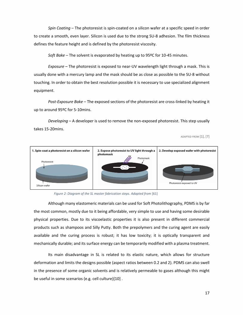
17
Spin Coating – The photoresist is spin-coated on a silicon wafer at a specific speed in order
to create a smooth, even layer. Silicon is used due to the strong SU-8 adhesion. The film thickness
defines the feature height and is defined by the photoresist viscosity.
Soft Bake – The solvent is evaporated by heating up to 95ºC for 10-45 minutes.
Exposure – The photoresist is exposed to near-UV wavelength light through a mask. This is
usually done with a mercury lamp and the mask should be as close as possible to the SU-8 without
touching. In order to obtain the best resolution possible it is necessary to use specialized alignment
equipment.
Post-Exposure Bake – The exposed sections of the photoresist are cross-linked by heating it
up to around 95ºC for 5-10mins.
Developing – A developer is used to remove the non-exposed photoresist. This step usually
takes 15-20mins.
ADAPTED FROM [1], [7]
Although many elastomeric materials can be used for Soft Photolithography, PDMS is by far
the most common, mostly due to it being affordable, very simple to use and having some desirable
physical properties. Due to its viscoelastic properties it is also present in different commercial
products such as shampoos and Silly Putty. Both the prepolymers and the curing agent are easily
available and the curing process is robust; it has low toxicity; it is optically transparent and
mechanically durable; and its surface energy can be temporarily modified with a plasma treatment.
Its main disadvantage in SL is related to its elastic nature, which allows for structure
deformation and limits the designs possible (aspect ratios between 0.2 and 2). PDMS can also swell
in the presence of some organic solvents and is relatively permeable to gases although this might
be useful in some scenarios (e.g. cell culture)[10] .
Figure 2: Diagram of the SL master fabrication steps. Adapted from [61]

18
In SL, obtaining a PDMS chip from a mold usually involves a few simple steps:
Mixing – the base and the curing agent are mixed with a 10:1 ratio. This ratio can be changed
depending on the desired properties (higher ratio produces a harder cured polymer).
Casting – The mixture is poured onto the mold and desiccated in a vacuum chamber for 30-
45min.
Curing – The polymer is cured on the mold at 60ºC to 80ºC for 1-4 hours.
Sealing – The PDMS is peeled off and exposed to oxygen plasma. The featured side is
brought into contact with the sealing material (glass, silica, or oxygen-activated PDMS) and forms a
watertight seal.
ADAPTED FROM [1], [7]
SL was adopted as the microfluidic fabrication technique of choice in many research
laboratories during the 2000’s because it allows the fabrication of complex microfluidic structures
and devices in a relatively simple way with a robust method, which make it practical for prototyping
different microfluidic designs, especially when coupled with the in-house printing of masks. It is also
possible to exploit some of the elastic properties of PDMS to build complex structures such as valves
[7] and 3D channels [11].
Soft Lithography’s main drawback is the difficulty in adapting both the fabrication process
and the designs to a mass-fabrication situation in a cost-efficient way. As has been reviewed above,
fabricating a PDMS chip through SL is a multi-step process and the final chips do not achieve the
physical stability required for long-term use. It also quite challenging to adapt a chip prototyped in
PDMS to other substrates for which industrial production has been developed - mainly injection-
molded thermoplastics. These drawbacks have held back the transition of many microfluidic
systems from a research setting to real-world applications.
Figure 3: Diagram of the SL PDMS casting steps. Adapted from [61]

19
2.3.2. Micro Injection molding
Micro IM is a polymer fabrication process which involves melting a thermoplastic in granule
form into a plasticization unit, and injecting it into a microstructured mold (Figure 4). The material
is subjected to a holding pressure and after some time it is cooled below the polymer’s glass
transition temperature and the part is demolded. A typical cycle lasts between few seconds to few
minutes [12]–[14].
Micro IM is well suited for the mass production of polymer microfluidic chips due to its short
production cycle and associated low production cost per piece. It also allows for the production of
relatively complex designs without added fabrication costs. Additionally, conventional IM has been
used for the production of many different plastic parts, with different compositions and quality
requirements and the knowledge acquired can be used when using Micro IM, automating the
production process or using different polymers, for example.
Conventional IM was first developed at the end of the 19th century with major
developments during the 20th century allowing for the production of progressively higher quality
pieces. Micro IM was first developed in the 1980’s using adapted conventional IM machines [12].
The main problems with this approach were the inaccuracy of the hydraulic controls, the waste of
material, and the degradation of the material during plasticization which limited the quality of the
Figure 4: Diagram of an Injection Molding cycle [13].

20
final pieces. These were partially solved by using electrical controls, smaller injection screw and
barrel and separating the plasticization and the injection (using a hot cylinder and a plunger instead
of a screw and a barrel).
Micro IM continued to be developed, with some commercial machines appearing in the last
decades [13]. These are capable of fabricating pieces from 0.08 to 8 cm3 with feature size ranging
from sub-micron to tens of microns, depending on the machine. This was achieved through many
distinct developments, namely the higher control of different process parameters (volume,
pressures, etc), the improvement in the transition from injection pressure to holding pressure, but
also through protocol optimization.
It was discovered that a critical parameter in the Micro IM process is the mold temperature
during injection. By raising the mold temperature near the Tg of the substrate and cooling it
afterwards (before ejection) it is possible to obtain micro-features with higher aspect ratio. This
process is called Variotherm in opposition to conventional IM where mold temperature is kept
roughly constant. Although necessary for the successful fabrication of small, higher aspect ratio
features, it does have some drawbacks. The heating and cooling steps greatly extend the cycle time;
and if the cooling is too fast it will introduce stress onto the piece, creating imperfections.
Due to the large number of parameters in a Micro IM process, the dependency of these on
different factors (mold material, feature size, total volume, etc), and their major influence in the
quality of the fabricated pieces, it is usually necessary and recommended [12], [15] to design and
run an optimization experiment whenever an element is changed, such as the substrate material or
the mold design. This is the main reason why prototyping a microfluidic design using IM is not an
efficient process, as each design change might take one to two weeks of optimization to translate
into a quality chip. This problem is compounded by the fact that a lot of the research in Micro IM
was developed for commercial reasons and is proprietary knowledge, making it harder for research
laboratories acquire the knowledge necessary to efficiently use Micro IM.
It is interesting to note that after parameter optimization feature quality will depend on the
mold fabrication method and quality, as in a HE process. As a general rule, mold designs should also
be limited to 2.5D features with no undercuts, again similarly to HE.
21
2.3.3. Hot embossing
Micro HE is a cost-effective replication technology, capable of transferring microstructured
patterns from a master mold onto a polymeric substrate. Although some work was done in micro-
patterning using hot-embossing before (vinyl LP fabrication), it was during the 1990’s that most of
micro hot embossing technology development was focused on MEMS production. The technique
used was LIGA (Lithographie, Galvanoformung, Abformung) which was capable of producing
complex polymeric micro structures with high aspect ratios, something not possible with other
fabrication processes at the time.
Thermoplastics consist of unlinked or weakly linked chain-like molecules that at a
temperature above the glass transition temperature (Tg) and below the melting temperature (Tm)
become plastic and can be molded into specific shapes, which will cure after cooling to temperatures
below Tg [16]. Micro HE is a method of exploiting this property to create micro-patterns from a pre-
built mold. As the polymer doesn’t undergo a phase change during hot embossing, the finished piece
presents little residual stress. The reduced temperature variation (compared to IM) also reduces the
piece shrinkage during cooling [17].
Developed in the 1990’s at Forschungszentrum in Karlsruhe, Germany, LIGA is a stepwise
microstructuring process followed by a HE step originally developed using X-ray lithography [18] but
which has since been adapted to use electron beam lithography, UV lithography and other similar
technologies [1]. It consists of four basic steps: (1) a contact lithography step, traditionally x-ray
lithography if high aspect ratio is necessary, (2) an electroplating step to create a metal layer (usually
nickel) on top of the patterned substrate, (3) the subsequent stripping of the substrate, with the
metal layer (or “shim”) acting as the mold, and (4) the hot embossing step. Nowadays UV-LIGA is
more common than X-ray LIGA due to its lower cost as it does not require a synchrotron, even
though it is not capable of producing features with such a high aspect ratio. The main drawback of
using LIGA to fabricate hot embossed microfluidic chips is the lengthy and sensitive electroplating
step, which can take up to 2 weeks for each mold, making truly rapid prototyping impractical. The
embossing step is usually performed with the use of a highly specialized machine which creates
vacuum conditions and is capable of precisely defining temperature and pressure. The demolding
process used has the drawback of leaving embossed chips with a relatively rough surface on the
unfeatured side. Due to its costly and lengthy process, LIGA is now only used in applications where
high aspect ratio and small dimensional tolerances are necessary.

22
A typical hot embossing process is composed of four major steps (Figure 5 and Figure 6).
The process starts with (1) heating of a thin polymer substrate and the mold to molding
temperature, followed by (2) an isothermal molding by embossing (velocity- and force-controlled),
(3) the cooling of the molded part to demolding temperature, maintaining constant pressure, and
(4) demolding of the components (mold and substrate) [19], [20].
On the heating step, temperature control is obviously extremely important and should be
accurate within 1ºC of the target temperature. The exact embossing temperature (Te) will depend
on the molded features (high aspect ratio-> higher temperature) and the material used but will
usually be around 10-30ºC above the glass transition temperature (Tg). The mold and the substrate
should be in contact during heating to make sure they are both at Te during embossing.
On the embossing step, the pressure increases and the substrate flows radially and into the
mold features [20]. The mechanisms for increasing the pressure can range from manually controlled
parallel platens pushing the substrate [21] and the mold together to an automated gas-pressure-
assisted system to guarantee pressure homogeneity [22]. The pressure is increased slowly to
prevent stress on the piece and maintained constant until demolding. By definition only the featured
mold area is counted towards the pressure calculation. The residual layer will be thinner for longer
Figure 5 Diagram of a Hot Embossing cycle. Adapted from Lai et al (2013).

23
embossing times (te) but it will always be present. This step usually takes 10-30mins depending on
the complexity of the design and the desired residual layer thickness.
The setup is then cooled actively or passively until the demolding temperature (Td). Td
depends on the feature design and demolding method and is usually 10-20ºC below Tg. The
demolding is the most critical step of the hot embossing process [20], [23] as small changes in Td can
cause a large variation in the force required to demold the piece, influencing the feature quality. If
Td is too high, there will be reflow of the plastic outside of the mold and the features less well
defined. If it is too low there will be strong adhesion forces between the feature walls and the mold
which will deform the piece upon demolding.
It is now possible to understand that a HE protocol can be nearly completely defined with
few simple process parameters: embossing temperature, embossing pressure, embossing velocity,
embossing time and demolding temperature. This makes HE a robust process, capable of producing
copies with little variability in feature quality [20], [24]. It also allows for easy description of
protocols, requiring only the description of the setup and the parameters used (Figure 6).
The main drawbacks of using HE for microfluidic fabrication are related to the difficulty of
adapting the process to large-scale fabrication in a cost-efficient way without losing the rapid-
prototyping capability. Efficiently fabricating multiple-copies molds, demolding large-area pieces
and long cycles are some of problems which have yet to be solved [23], [25].
Figure 6: Pressure and Temperature diagram of a Hot Embossing cycle. Ideally a hot embossing protocol can be fully described by an identical diagram. The temperature is in red and the pressure in blue.

24
Having described the three major polymer microfluidic fabrication methods, it is useful to
review their main capabilities and constraints (see Table 1).
IM is a mature technology which has been adapted to successfully produce many different
microfluidic designs. Its main advantage is the extremely low cost of making large number of copies
of the same design. Each design requires extensive process parameter optimization, making it
unsuitable for rapid prototyping.
SL is an extensively used microfluidic fabrication technique which allows for the rapid
fabrication of complex designs in elastomeric polymers. Its main disadvantage is the difficulty in
transferring a design prototyped in PDMS to a mass-produced (Injection Molded) design in
thermoplastic.
HE is a simple, robust fabrication technology capable of producing high quality microfluidic
polymer chips. Its main advantage is the capability of producing thermoplastic microfluidic chips
with little optimization necessary provided there is a suitable mold. It is straightforward to mass-
produce designs prototyped with HE. Its main disadvantage is being unsuitable for large scale
production, as it is non-trivial to emboss multiple copies of one design at once and each fabrication
cycle takes several minutes, a long time when compared to seconds in IM.
Fabrication Method Advantages Disadvantages
Soft Lithography Cost-effective, able to fabricate
3D geometries, high resolution
Pattern deformation, vulnerable
to defect
Injection Molding
Easy to fabricate complex
geometry, fine features, and 3D
geometries, low cycle time, mass
production, highly automated
Restricted to thermoplastics, high
cost mold, difficult to form large
undercut geometries
Hot Embossing
Cost-effective, precise, and rapid
replication of microstructures
with low structural stress
Restricted to thermoplastics,
difficult to fabricate complex 3D
structures
Table 1: Summary of the various fabrication methods. Adapted from [26].

25
2.4. Mold Fabrication
Provided the HE setup and protocol are adequate, the quality of hot embossed features
depends mostly on the quality of the mold [27]–[29]. It is then of upmost importance to carefully
evaluate the mold fabrication process when considering HE for microfluidic fabrication. Different
methods will produce molds with different materials and physical properties. HE molds should be
thermally resistant up to the embossing temperatures, thermally conductive, rigid and structurally
resistant to several embossing cycles. In a rapid-prototyping scenario molds should also be quick
and simple to fabricate at a low cost, allowing for multiple design changes.
The most common mold fabrication methods for microfluidic systems are
photolithography-based methods (e.g.: SU-8 on silicon wafers, secondary polymeric molds and
electroplated molds) and direct-structuring methods (e.g.: micro-milling, micro electric discharge
machining, laser structuring). All of these are suitable for different applications outside mold
fabrication as well, but are widely used to create HE molds because they are capable of creating
permanent surface patterns on the nanometer and micron scale. It is interesting to note that
although many microfluidic devices have sub-micron features, most Lab-on-a-chip systems smallest
features are over 50 μm [4].
As was mentioned before, Electroplating has been used as a mold fabrication method for
hot embossing, usually in a LIGA process [30]. Electroplating is a technique used to coat a metal
piece with a thin film of other metal by applying a current between the piece and the source metal.
The piece acts as the cathode and the source as the anode with both being immersed in a plating
bath whose composition facilitates the electrodeposition reaction. Ideally, the metal coating
adheres permanently to the piece.
Although the distinction is sometimes not mentioned in literature, most “electroplated”
molds are in fact fabricated through electroforming and not electroplating. Both techniques exploit
the electrodeposition phenomenon but whereas electroplating is directed at creating a metal
coating on a piece, electroforming is directed at creating a metal piece from a non-metallic master.
In electroforming a master form is made conductive through the application of a thin coating and
the electrodeposition process is performed identically to an electroplating protocol but it is ran for
much longer periods of time so that it forms a thicker layer (up to 1 mm) [31]. The master is then
removed and the created metal piece is used as the HE mold, for example. HE molds are usually
26
made from Nickel due to its rigidity, good thermal properties and ease of use in electrodeposition
[32].
Both of this techniques are slow processes with electroforming protocols usually lasting for
1-2 weeks to obtain HE molds with the thickness and quality required [33]. In addition to that,
electrodeposition usually requires extensive knowledge and parameter optimization (current
applied over time, bath composition) to obtain good results [34]. Its main advantage is the capability
of creating metal molds with good surface quality and small feature size (< 1 μm).
Depending on the goals of the design, using conventional SU-8 photoresist on silicon wafers
might be possible [35]. These can allow the use of well-established, versatile lithography methods
while being adequate for rapid-prototyping. These usually produce molds less durable than other
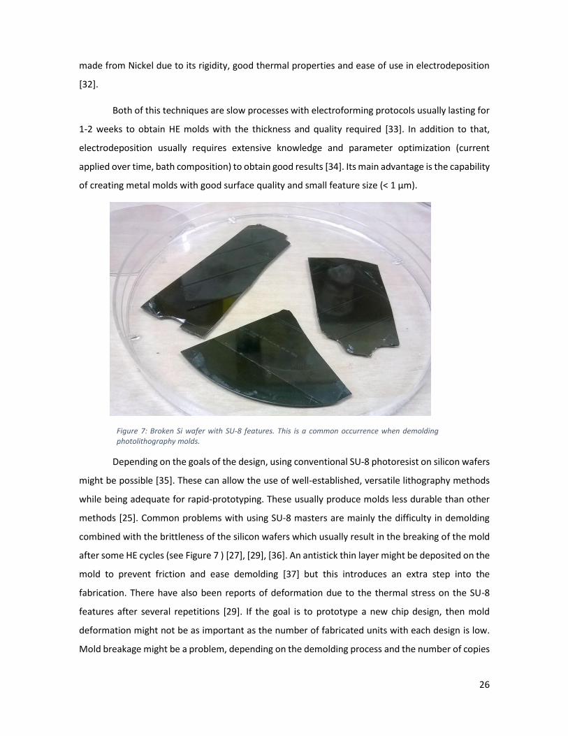
methods [25]. Common problems with using SU-8 masters are mainly the difficulty in demolding
combined with the brittleness of the silicon wafers which usually result in the breaking of the mold
after some HE cycles (see Figure 7 ) [27], [29], [36]. An antistick thin layer might be deposited on the
mold to prevent friction and ease demolding [37] but this introduces an extra step into the
fabrication. There have also been reports of deformation due to the thermal stress on the SU-8
features after several repetitions [29]. If the goal is to prototype a new chip design, then mold
deformation might not be as important as the number of fabricated units with each design is low.
Mold breakage might be a problem, depending on the demolding process and the number of copies
Figure 7: Broken Si wafer with SU-8 features. This is a common occurrence when demolding photolithography molds.

27
required. Photoresist molds usually present very smooth walls and surface finish but are limited to
around 100 μm thick features.
Other fabrication methods used in the literature were the casting of secondary molds from
SU-8 primary molds in order to overcome the structurally deficiencies of silicon wafers while
retaining the advantages of photolithography. Epoxy resin, thermoplastics with high Tg and PDMS
[36], [38] have all been used. Overall there were improvements over using SU-8 molds but also some
additional problems with this approach, mainly the poor dimensional stability of PDMS and the low
embossing temperatures possible with epoxy or thermoplastics. Besides this, all the restrictions of
using photolithography are still present with the added step of fabricating a secondary mold.
Another interesting approach is performing SU-8 photolithography on a copper substrate
instead of a silicon wafer [37]. This allows for a much stronger mold with better thermal properties
while retaining the benefits of using photolithography. Besides the normal photolithography
restrictions there is also the added issue of properly polishing and cleaning the copper substrate to
obtain good adhesion between the photoresist and the copper wafer.
28
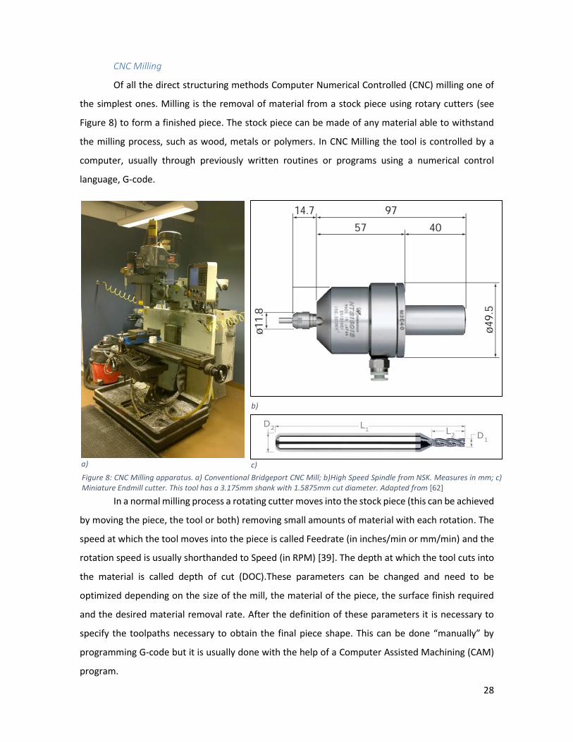
CNC Milling
Of all the direct structuring methods Computer Numerical Controlled (CNC) milling one of
the simplest ones. Milling is the removal of material from a stock piece using rotary cutters (see
Figure 8) to form a finished piece. The stock piece can be made of any material able to withstand
the milling process, such as wood, metals or polymers. In CNC Milling the tool is controlled by a
computer, usually through previously written routines or programs using a numerical control
language, G-code.
In a normal milling process a rotating cutter moves into the stock piece (this can be achieved
by moving the piece, the tool or both) removing small amounts of material with each rotation. The
speed at which the tool moves into the piece is called Feedrate (in inches/min or mm/min) and the
rotation speed is usually shorthanded to Speed (in RPM) [39]. The depth at which the tool cuts into
the material is called depth of cut (DOC).These parameters can be changed and need to be
optimized depending on the size of the mill, the material of the piece, the surface finish required
and the desired material removal rate. After the definition of these parameters it is necessary to
specify the toolpaths necessary to obtain the final piece shape. This can be done “manually” by
programming G-code but it is usually done with the help of a Computer Assisted Machining (CAM)
program.
Figure 8: CNC Milling apparatus. a) Conventional Bridgeport CNC Mill; b)High Speed Spindle from NSK. Measures in mm; c) Miniature Endmill cutter. This tool has a 3.175mm shank with 1.5875mm cut diameter. Adapted from [62]
b)
a) c)

29
Figure 9: Different milling types. Climb milling is usually chosen for micro-milling but Conventional Milling is used for micro-milling as it minimizes mill deflections perpendicular to the direction of cut.
Micro-milling is the application of CNC Milling to small-sized structures, although the
distinction between macro and micro scale milling isn’t well defined. Micro-milling, also called
micro-machining, has been used to fabricate microfluidic molds with features under 100 μm. The
size limiting factors in micro-milling are the size of the tools and the relatively high roughness
present in small features. It is extremely well suited for mold fabrication as it allows for arbitrary
design changes (including thick features), has few process parameters, and is capable of quickly
producing metal molds.
Although the overall principle is identical, there are some differences between normal
milling and micro milling. The critical part of milling is maintaining a high angular velocity, to allow
the tool to cut into the piece. As the tools become smaller (see Figure 10) this requires having faster
rotational speeds with high speed machining (HSM) starting at 10 000 RPM and ultra-high-speed
machining (UHSM) at 100 000 RPM. This is a problem in reusing existing CNC mills meant for macro-
scale milling as they are usually only capable of speeds up to 10 000 RPM. There are HS and UHS
spindles which allow adapting machines for higher speeds but it does represent an additional cost.
Other common issue is that CNC mills built for macro-milling usually have a minimum step size (the
minimum distance the tool can be moved in any direction) of 1-3 μm which prevents the definition
of micron-sized toolpath features. Due to the small size of the tools extra care must be taken to
account for the lower rigidity of the tools. As tool breakage is more common than in macro-milling
and smaller tools cost more than larger ones, the running costs of micro-milling will also be higher.

30
Comparing to other mold fabrication techniques, its main disadvantages are the relatively
high surface roughness and minimum milling size limitations. The surface roughness can be reduced
by optimizing the process parameters or by polishing the mold [40] although it will always be
present. Its main advantages are the fast fabrication time, being able to produce metal molds and
the low cost per mold.
Figure 10: Microphotograph of a micro end-mill with 200 μm diameter. Notice the large size ratio between the shank and the cutting edge diameters. Adapted from [63]

31
3. PCR
Introduced into the scientific community during the 1980’s, PCR is a technique that allows
for exponential amplification of DNA without the need to clone into vectors [41]. PCR has become
an essential part of biological and biomedical research as well as medical diagnosis. It allows the
detection and diagnosis of infectious diseases; genetic analysis of various kinds; forensic analysis,
among other uses. PCR-based diagnosis methods allow the detection of pathogens with high
sensitivity and sensibility [16], [42].
PCR relies on thermal cycling - heating and cooling the DNA sample to specific temperatures
- in the presence of primers, DNA polymerase and Deoxynucleoside triphosphates (dNTPs). Primers
are small strands of nucleic acids which are complementary to specific target regions of the DNA
strands.
The conventional PCR protocol consists of 20-35 thermal cycles with each cycle having 3
target temperatures (see Figure 11). There is usually an initialization step at 94-96 ºC before the
thermocycling. During the heating (Denaturation) step (94-98 ºC), DNA melting occurs and DNA
strands are separated, forming single-stranded DNA molecules. The temperature is then lowered
(Annealing step) to 50-65 ºC depending on the primers used. During this step primers attach to
single stranded DNA. Temperature is raised again for the elongation step, with the exact
Figure 11: Diagram of a 3-step PCR thermocycling protocol. Adapted from [64]
32
temperature depending on the DNA polymerase used. The DNA polymerase (more commonly Taq
polymerase) then synthesizes a complementary DNA strand, initiating the process on the attached
primers and using the dNTPs present. This cycle is repeated multiple times, duplicating the target
DNA sequence with each cycle and allowing for an exponential amplification.
Over the years, many PCR protocol variants were developed, allowing for multiple primers,
different polymerases and faster thermocycling protocols.
3.1. Miniaturization of PCR
“Miniaturization of PCR provides many advantages, such as decreased cost of fabrication
and operation, decreased reaction time for DNA amplification, reduced cross talk of the PCR
reaction, and ability to perform large numbers of parallel amplification analyses on a single PCR
microfluidic chip.” [43]
The first PCR microdevices developed were focused on improving the reaction/amplification
speed and were fabricated in silicon. Silicon has a high thermal conductivity and allows for very fast
temperature ramp times, resulting in very short on-chip protocols [44]. It is also possible to integrate
heaters and sensors directly into the chip. Despite these advantages, silicon presents some critical
flaws as a PCR-chamber substrate as bare silicon has an inhibitory effect on the PCR reaction and
fabricating a functional device required a highly complex protocol and design, and there is a lack of
available rapid prototyping techniques. As an alternative, glass was used as a substrate for PCR-
chambers in Lab-on-a-chip devices, as it presents well-defined surface chemistry and is optically
transparent.
Recently, various polymers have started to become the substrate of choice for PCR-based
devices [45], as the focus shifted from reaction speed to integration in Point-of-Care devices. In this
case the goal is not just to obtain a faster reaction time but also to obtain PCR amplification using
small reagent volumes with little user input in a cheap and disposable chip.
Point-of-care testing is defined as near-patient testing in a hospital, doctor’s office, clinic,
or home [46] and can have an important impact in low-resource settings where there is a lack of
centralized laboratories or when timing is critical, in emergency triage for example [43]. There is
also an opportunity in providing rapid, low-cost tests for home or clinic use [47].

33
Due to the need for POC to be disposable and low-cost, thermoplastic polymers have
emerged as the substrate of choice for these devices. As was mentioned above, IM allows for the
mass-production of microfluidic chips at a low cost per device.
There have been some academic [48]–[51] and some commercial solutions [52] but there
has yet to appear an example of a truly simple to use integrated platform. So far all FDA-cleared PCR
test kits to-date are still categorized as high or moderate complexity [53], meaning they are still
required to be used by a trained professional. This has happened due to the difficulty in integrating
many different functions, namely sample preparation, amplification and detection, necessary for a
PCR-based diagnostic device while retaining a simple, low-cost design. POC device development
requires the focus on the final application to be present along the development process, so that
end-use restrictions are accounted for at every step of the process.
In terms of PCR miniaturization, it is useful to note that most of the approaches can be
classified into either single-chamber PCR or Continuous Flow PCR (CF-PCR) (see Figure 12). Single-
chamber designs were the first ones to be developed and are characterized by their smaller
minimum sample volume and simpler system configuration. A chamber is filled with PCR reagent
mixture and some form of temperature control heats the contents, identical in function to a
conventional thermocycler.
In a CF-PCR design the PCR mixture is transported over different zones of the chip, with each
zone at different pre-fixed temperatures in order to emulate thermocycling. CF-PCR designs are
usually characterized by simpler thermal control mechanisms and the need to have precise flow
control.
Figure 12: Schematic illustrations of types of microfluidic PCR chip designs. a) stationary chamber system b) continuous flow system. Adapted from [65].

34
4. Methodology
As was previously mentioned, there is a current need for a viable rapid prototyping method
for hard plastics microfluidics. Due to its simplicity, robustness and polymer molding capabilities Hot
Embossing was chosen as the basic fabrication technique for a rapid prototyping method. Although
much of the existing work in micro-scale Hot Embossing was performed using dedicated machines
and labor-intensive molds, there are reports of microfluidic chips fabricated using only a minimal
setup with temperature control provided by a hot plate and pressure control with a pre-defined
weight [51], for example.
The goal with this experimental work was to develop and test the capabilities of a
prototyping system based on a HE minimal setup consisting only of a hot press and a mold. This
setup should allow us to fabricate chips with good feature quality (dimensional stability, lack of
imperfections, reasonable surface quality, etc); should be reliable and robust, requiring little
optimization between different designs and producing identical copies with unchanged parameters;
should allow the fabrication of different designs in a short amount of time, requiring both the
embossing and the mold fabrication process to be relatively short.
Some initial work was necessary to identify whether this minimal setup was capable of
fabricating chips with the required quality or if additional equipment was necessary (dedicated HE
machine, automated temperature or pressure control, etc); and to compare mold fabrication
methods. After the definition of a working embossing protocol and mold fabrication method the
suitability of this setup for rapid prototyping was tested in the development of a PCR chamber
microfluidic chip. The goal was to test the developed fabrication setup by iterating on a previous
chip design towards an integrated and disposable PCR chip. This example was chosen mainly
because it is a non-trivial challenge, with functionality highly dependent on chip design (chamber
size, geometry, etc). It was also integrated into other projects in the laboratory so it was possible to
leverage the existing knowledge of the PCR process.
The first experiments were focused on testing different hot embossing protocols [20], [23],
[32], [37], [54], [55] using different mold materials and fabrication methods. After defining a
protocol and CNC Milling as the standard mold fabrication method, PCR chips were designed and
fabricated, iterating the design as necessary. CNC Milling was chosen due to its versatility, ease of
use and the production of metal molds.

35
The main goals of the PCR chamber development were to evaluate how fast the fabrication
setup could produce a chip with a new design in a reliable way and whether CNC Milling could
produce molds with the desired features (minimum feature size, reasonable surface quality, etc). A
secondary goal was obtaining in-chip DNA amplification with a simple microfluidic system. The
embossing protocol and method continued to be optimized during this process to ease the filling
and demolding of deep features. All the designs were embossed both in Polycarbonate (PC) and
Cyclic Olefin Polymer (COP) substrates but due to the lack of a suitable sealing method, results were
only obtained for PC chips.
The PCR experiments were based on the GeneAmp Fast PCR protocol and the amplification
target was the IS6110 gene from M. tuberculosis genomic DNA. All the sample preparation steps
were performed off-chip.
Sample preparation protocol:
a) The bench area and all the items needed were bleached beforehand
b) All the reagents were kept on ice
c) 10µL of primer mastermix were made with 1µL forward primer, 1µL reverse
primer and 8µL of Nuclease-Free water
d) For each sample to be analyzed, 10 µL PCR mastermix 2x (GeneAmp), 1 µL of
primer mastermix and 8.5 µL of Nuclease-Free water were mixed in a 1.5 mL
Eppendorf tube to make the PCR mastermix.
e) For each sample, 19.5 µL of PCR mastermix was mixed with either 0.5 µL of TB
gDNA (10 µg/mL) or 0.5 µL of Nuclease-Free water, depending on whether it
was a positive or negative control.
Gel electrophoresis protocol:
a) 600 mg of agarose was weighed and mixed with 30mL TAE buffer (1x) in an
Erlenmeyer flask
b) The flask was covered with Kimwipes and the mixture was repeatedly heated
and mixed in a microwave for 30s at a time until the liquid was clear and streak
free.
c) The solution was allowed to cool until 60ºC, measured with a thermometer.
d) 3 µL of SYBR Green were mixed with the solution and it was poured on the gel
mold, swirling the mold.

36
e) The gel was covered with foil and left to set for 30 min.
f) After thermocycling the PCR product tubes were put on ice and 10uL of each
product was mixed with 2 µL Orange dye.
g) The first well was loaded with 5 µL of DNA ladder and the others with 10 µL of
dyed PCR product.
h) The settings used for the electrophoresis were 100V and 50mA and it was ran
for 45 min.
i) The gel was placed in a petri dish and covered with foil.
j) The gel was then analyzed using a UV-light imager.
SU-8 mold fabrication Protocol:
a) A Si wafer was placed on the spinner, centered on the spinner chuck, and the
vacuum was activated.
b) 2mL of SU-8 3050 photoresist were deposited on the Si wafer.
c) The spinner was ran for 5s at 500 rpm and then for 30 s at 3000 rpm.
d) After turning off the vacuum the coated Si wafer was baked for 15 minutes at
95ºC and then left to cool to room temperature.
e) The wafer was centered underneath a UV lamp and covered with a UV Mask.
f) The setup was then exposed for 30s to UV light.
g) The Si-wafer was then covered with foil and transferred onto a hot plate at 95ºC
for 5 min.
h) The wafer was transferred into a dish of SU-8 developer and was gently agitated
for 5 minutes and afterwards was rinsed with IPA. This process was repeated
until the wafer was cleaned of white residue.
i) The wafer was finally let to dry in air.

37
PDMS casting protocol:
a) PDMS curing agent and PDMs base were thoroughly mixed on a 1:10 ratio for a
total weight of 35g.
b) This mixture was then poured over mold on a Petri dish and placed in a
desiccator for 45min.
c) The dish with PDMS was cured in an oven at 75ºC for 1 hour.
d) The PDMS was then peeled off the mold
e) For mold quality studies a ~1mm cross-section was then cut with a blade.
4.1. Materials
The substrate polymers used were PC from McMaster-Carr and COP (ZEONOR 1420R) from
Zeon Chemicals, in sheets with different thicknesses from 1mm to 2.5mm. These substrate materials
were chosen for their high glass transition temperature, optical clarity, biocompatibility, rigidity,
and commercial availability [56], [57].
The designs and molds were drawn using the CAD program SolidWorks 2013 (Dassault
Systèmes) and the milling toolpaths were created and exported through the Mastercam X6 for
SolidWorks plugin (CNC Software, Inc.).
The metal molds were fabricated using a 3-axis EZTRAK Bridgeport CNC vertical mill and
various carbide end mills (Microcut and Harvey Tool) with diameters from 1/4in to 0.002in,
depending on the desired features. For tools smaller than 1/8in an Ultra-High-Speed Spindle
(Nakanishi HTS1501S-M2040) was used, with a fixed rotation speed of 150 000 rpm, so as to maintain
a high cutting speed with a small cutting tool diameter. After milling and the removal of any burrs
the molds were sonicated with DI water for 10 mins.
The mold materials tested for CNC milling were MIC 6 Aluminum and C360 Brass (McMaster-
Carr). These were selected for their low-cost and availability, good machinability and good thermal
properties. MIC 6 Aluminum is cast, presenting very low internal stress and good dimensional
stability. It is available as extremely flat plates, preventing the need for extra milling and reducing
the fabrication time. C360 Brass is also called free-cutting or free-machining brass due to its
extremely good machinability. It has a small percentage of lead which acts as lubricant during
milling, eschewing the need for lubricant while producing small chips. For other metal pieces 6061
Aluminum (McMaster-Carr) was used due to its rigidity and low-cost.

38
In the photolithography-based mold fabrication, SU-8 3050 (Microchem) was spun on
Silicon wafers and exposed to UV light through patterned masks. After development, the patterned
silicon wafers were then used directly as the HE molds.
The hot embossing itself was performed using a manual press (Model C 3851 Carver) with
manually controlled aluminum heated platens (2101 Carver). The pressure and temperature was
monitored by reading the force and temperature gauges.
The embossed chips were cleaned with DI water, Isopropanol, DI water, and Ethanol
(Thermo Fisher Scientific) and dried with compressed Nitrogen.

39
5. Results and Discussion
5.1 Testing Hot Embossing protocols and mold fabrication methods
The first Hot Embossing experiments were performed on a PC substrate using a previously
machined aluminum mold (Figure 13). This was used to test different protocols, changing embossing
temperature, embossing time, embossing pressure and demolding temperature. The temperature
was controlled using a thermostat on each platen, the pressure was manually controlled, and
demolding was performed by hand.
After some testing it was possible to heat up to the embossing temperature on each platen
without overshooting the target in under 10 minutes. By turning the heaters on/off as necessary is
was possible to maintain a constant temperature (+/- 1.5 ºC). The cooling down was passive, with
the heaters turned off. Depending on the embossing and demolding temperatures the cooling down
usually took anywhere from 20 min to 30 min.
Figure 13: Hot Embossing Equipment: a) Hot press with temperature (red) and pressure (cyan) controls; b) Aluminum mold on the PC substrate before embossing; c) Aluminum mold with embossed pieces.
b)
a) c)

40
As expected the minimum embossing temperatures were around 15 ºC above glass
transition temperature of PC (146ºC). Chips embossed at lower temperatures presented low optical
clarity and incomplete filling of some features. Embossing pressure used was around 22MPa as the
minimum force possible was around 500 pounds-force and the mold had an area of 10mm x 10 mm.
The exact pressure value was found to not be a critical parameter, as long as it remained constant.
One interesting find was the importance of the rate of pressure increase, from contact
pressure to embossing pressure, something rarely mentioned in the literature. A slow rate (0->Pe in
60s) was found to produce substantially better feature filling. Another important fact was the
difficulty in separating the mold from the piece after embossing (demolding), most likely due to the
high vertical walls of the mold. Although mentioned in the literature, this problem is usually
minimized as the features embossed are shallower, with smooth surfaces (LIGA, etc), and therefore
present lower adhesion forces between the mold and the piece. One common solution to this
problem is the use of a release agent between the mold and the substrate but this adds to the
duration and complexity of the embossing process
SU-8/Silicon molds were also tested using identical protocols but were found to be
extremely fragile and would often break during embossing and demolding (Figure 14). The features
(straight channels 100-500 µm wide, 100 µm deep) were embossed with good quality, presenting
no defects. The good embossing quality makes SU-8/Silicon molds a feasible alternative to CNC
Milled molds, as it allows for the use of designs, knowledge and equipment developed for SL. In a
rapid prototyping scenario this setup presents some limitations as it will be hard to obtain a
reasonable number of copies (>3) from the same mold and design changes become dependent on
the time it takes to obtain a UV-mask with a new design (usually over 24h).
Figure 14: Pieces of a broken SU-8/Silicon mold.

41
In order to test the minimum resolution possible with CNC Milling and minimal setup HE, a
test mold with straight channels (50 µm channels 50 µm apart, 100 µm channels 100 µm apart and
150 µm wide channels 150 µm apart) was designed and milled in aluminum. As this was the first
contact with Micro Milling, there were some problems in the fabrication: the milled channels were
narrower than desired, presented rough walls, the depth of the channels wasn’t consistent between
thinner and wider channels and the milling tool used was damaged during fabrication. After
troubleshooting, it was found that there were some errors in the toolpath definition, the DOC and
feedrate hadn’t been properly adjusted to account for the high rotational speeds and small diameter
and that precise calibration of the Z-axis between each tool change was critical. The milling quality
was tested through visual inspection of the molds and of cross-sections obtained through PDMS
casting (Figure).
The embossing process was successful, reproducing the milled features as expected (Figure
16). It was useful to notice that even thin and deep mold features were filled and successfully
embossed.
Figure 15: Cross-sections of the milled channels obtained through PDMS casting. Left- wider channels (150 µm design). Notice the smooth walls and shallow depth of cut. Right – Thinner channels (50 µm design). Notice the deep, milled features and the thin standing ones.
Figure 16 : Embossed PC chip. Left- wider channels (150 µm design). Right – Thinner channels (50 µm design). Notice the accurate embossing of all the features, including the characteristic machining texture.
42
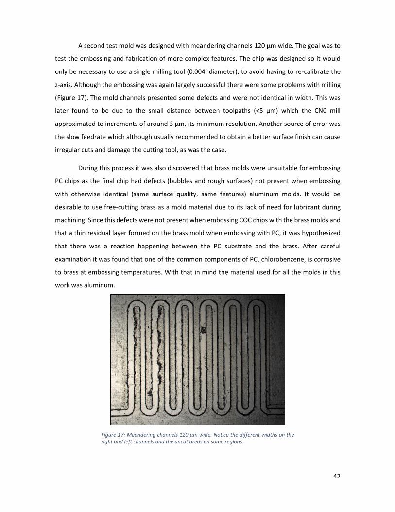
A second test mold was designed with meandering channels 120 μm wide. The goal was to
test the embossing and fabrication of more complex features. The chip was designed so it would
only be necessary to use a single milling tool (0.004’ diameter), to avoid having to re-calibrate the
z-axis. Although the embossing was again largely successful there were some problems with milling
(Figure 17). The mold channels presented some defects and were not identical in width. This was
later found to be due to the small distance between toolpaths (<5 μm) which the CNC mill
approximated to increments of around 3 μm, its minimum resolution. Another source of error was
the slow feedrate which although usually recommended to obtain a better surface finish can cause
irregular cuts and damage the cutting tool, as was the case.
During this process it was also discovered that brass molds were unsuitable for embossing
PC chips as the final chip had defects (bubbles and rough surfaces) not present when embossing
with otherwise identical (same surface quality, same features) aluminum molds. It would be
desirable to use free-cutting brass as a mold material due to its lack of need for lubricant during
machining. Since this defects were not present when embossing COC chips with the brass molds and
that a thin residual layer formed on the brass mold when embossing with PC, it was hypothesized
that there was a reaction happening between the PC substrate and the brass. After careful
examination it was found that one of the common components of PC, chlorobenzene, is corrosive
to brass at embossing temperatures. With that in mind the material used for all the molds in this
work was aluminum.
Figure 17: Meandering channels 120 μm wide. Notice the different widths on the right and left channels and the uncut areas on some regions.

43
5.2 Development of a hard polymer PCR chip
In order to test the practicality of using HE for microfluidic fabrication it was used in the
development of a PCR microfluidic chip. The work began with using a previously tested design and
adapting it to create a HE mold. The previous design had been fabricated by CNC milling directly on
a PC substrate (Figure 18) and the SolidWorks (SW) drawings were adapted to build a HE mold. This
design was tested, optimized and tested again. The design was changed multiple times using the
developed prototyping workflow and it was possible to obtain PC chips of each design in under 6h.
The initial setup consisted of a reaction chamber and a temperature sensing chamber in a
PC square chip, with an external thermoelectric heater placed under the chip. The reactions
chamber was filled with the PCR reagents and the sample, with the temperature sensing being
performed by a thermistor (Custom Electric). The chambers were sealed using acetonitrile and
120μm thick PC film and the inlets were sealed using adhesive tape. The heater was controlled with
a simple ON/OFF feedback mechanism controlled by an Arduino UNO microcontroller with input
from the thermistor. The temperature was monitored on a computer monitor connected to the
microcontroller as well. The goal was to thermocycle the sample in order to obtain DNA
amplification and to calibrate the system so that in the future only external sensing would be
necessary.
Figure 18: PCR chip with features directly milled on the PC substrate
44
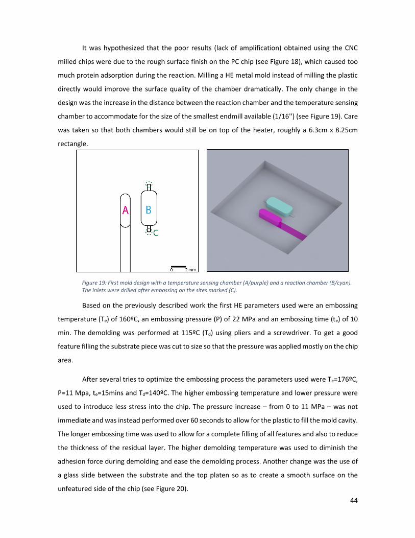
It was hypothesized that the poor results (lack of amplification) obtained using the CNC
milled chips were due to the rough surface finish on the PC chip (see Figure 18), which caused too
much protein adsorption during the reaction. Milling a HE metal mold instead of milling the plastic
directly would improve the surface quality of the chamber dramatically. The only change in the
design was the increase in the distance between the reaction chamber and the temperature sensing
chamber to accommodate for the size of the smallest endmill available (1/16'') (see Figure 19). Care
was taken so that both chambers would still be on top of the heater, roughly a 6.3cm x 8.25cm
rectangle.
Based on the previously described work the first HE parameters used were an embossing
temperature (Te) of 160ºC, an embossing pressure (P) of 22 MPa and an embossing time (te) of 10
min. The demolding was performed at 115ºC (Td) using pliers and a screwdriver. To get a good
feature filling the substrate piece was cut to size so that the pressure was applied mostly on the chip
area.
After several tries to optimize the embossing process the parameters used were Te=176ºC,
P=11 Mpa, te=15mins and Td=140ºC. The higher embossing temperature and lower pressure were
used to introduce less stress into the chip. The pressure increase – from 0 to 11 MPa – was not
immediate and was instead performed over 60 seconds to allow for the plastic to fill the mold cavity.
The longer embossing time was used to allow for a complete filling of all features and also to reduce
the thickness of the residual layer. The higher demolding temperature was used to diminish the
adhesion force during demolding and ease the demolding process. Another change was the use of
a glass slide between the substrate and the top platen so as to create a smooth surface on the
unfeatured side of the chip (see Figure 20).
Figure 19: First mold design with a temperature sensing chamber (A/purple) and a reaction chamber (B/cyan). The inlets were drilled after embossing on the sites marked (C).

45
Despite the higher Td, demolding was still a problem due to the long and deep vertical walls
which created strong adhesion forces. In order to ease the demolding process a perforated metal
shim (0.5mm thick) was placed between the substrate and the mold during embossing. The
demolding was then performed by removing the metal shim which pulled the piece out of the mold.
The inlets (C) were milled directly on the chip with a 1mm mill on a drill press. The chips were
cleaned with DI water, IPA, ethanol and DI water again and dried with compressed Ni.
Figure 20: Diagram of embossing setup. Both the top and bottom platens were heated and had integrated temperature sensors. Notice the glass slide between the substrate and the top platen.

46
5.2.3. PCR experiments
After optimizing the embossing parameters, 3 identical copies were embossed as described
above. A PCR experiment was set up with a negative and a positive control off-chip – the
thermocycling was conducted in a conventional thermocycler - and 3 different on-chip experiments.
The sample used was M. tuberculosis genomic DNA and the amplification target was the IS6110
gene. The on-chip experiments were designed to try to pinpoint possible failure points along the
process. One sample was placed on-chip for 5 minutes with no thermocycling, a second was
thermocycled for only 5 minutes, and a third went through the full thermocycling (35 cycles). The
thermocycling was done according to a Fast PCR Protocol (GeneAmp Fast PCR) with only two
temperature steps.
For thermocycling the chips were filled with the PCR reagent mix using a micropipette and
sealed with adhesive tape for the required duration. The sealed chip was placed on top of the heater
and fixed in placed with the help of a milled PC piece and two binder clips. All the samples were
tested at the same time using gel electrophoresis.
As can be seen in Figure 21, no amplification was detected in any of the on-chip samples. It
was hypothesized that this might have been due to the surface roughness of the inlets causing
protein adsorption, as these were machined after embossing the chip
Figure 21: PCR amplification results obtained through gel electrophoresis. A- DNA ladder; B-Negative Control; C- Conventional thermocycling; D – Conventional thermocycling with 5 min incubation on-chip; E- 5 min on-chip thermocycling + conventional thermocycling; F – On-chip thermocycling only. Only the existence of amplification was being tested.

47
In order to eliminate any post-embossing machining, a new mold which incorporated the
inlets was designed and milled. Another minor change was the increase in depth of the thermistor
wires' cavity. Although the parameters used were the same as the previous mold, it was not possible
to get a good filling and easy demolding at the same time. After experimenting with different
parameters and still not obtaining satisfactory results the mold setup was changed.
A "two part" mold (Figure 22) was developed so that the strong adhesion forces around the
chip would help the demolding process instead of hampering it. The top part of the mold was CNC
milled on 2mm thick stock Aluminum sheet with room for the chip features (20mm x 20mm, in
orange) and alignment features (green). The bottom part was CNC milled and included both the chip
features (inlets - red, reaction chamber - cyan, thermal chamber - purple) and the alignment
features (dark blue). This setup allowed for the use of different bottom chip designs while
maintaining the same top part. The demolding was done by separating the top and the bottom parts
by hand using sheepskin gloves and pliers.
Figure 22: Two part mold. a) Top part with a 20 x 20mm square (orange) defining the chip size and alignment features (green). b) Bottom part with chambers, inlets and alignment features (dark blue). c) Assembled two part mold with color highlights
a)
b)

48
By using this setup it was possible to obtain good chips, with no problems in filling or
demolding. It was also much easier and faster to demold after removing the piece from the hot
press. This setup also allowed for different chip designs while maintaining the same chip dimensions.
Five more chips were produced and sealed and the experiment was ran with an identical
protocol to the previous one. The results were the same as before with no DNA amplification
detected in chips where heating occurred.
Having ruled out surface roughness as the main problem and after reviewing the design,
temperature control was pinpointed as the most likely point of failure - the thermistor was found
to be far from an ideal temperature sensor, as it was not in contact with water or other similar liquid;
it was relatively slow reacting; and it had a large mass which could complicate the calibration
afterwards.
With that in mind a new design was proposed and tested (Figure 23). It consisted of two
identical chambers side by side with one being the reaction chamber and the other the temperature
sensing chamber. The temperature sensing would be performed by a small thermocouple (Custom
Thermoelectric) instead of the thermistor due to its much smaller size and faster response. During
preliminary testing this design presented some issues, mostly integrating the thermocouple into the
chamber while maintaining good sealing between the chip and the film. It was also discovered that
there were large temperature differences inside the chamber. During heating the temperature at
the bottom of the chamber, in contact with the heater, was considerably hotter than at the top. This
also produced the secondary effect of some regions of the chamber taking a long time to reach the
target temperatures.
Figure 23: Two chamber design. Inlets – red; reaction chamber – cyan; thermal chamber – purple.

49
To avoid this phenomenon a new design was proposed (Figure 24). The main requirements
were to maximize the contact area between the chamber and the heater and to minimize the height
of the chamber, while maintaining a minimum volume (8-10μL). The positioning and shape of the
inlets and corners was also taken into consideration to try to minimize bubble formation. The chip
was also made thinner (1 mm vs 2 mm) to decrease the thermal mass of the chip. With the new
design it became impossible to measure the temperature inside the chamber during the
thermocycling as any thermal sensor might interfere with the PCR reaction. The solution to this was
to calibrate the temperature on the outside of the chamber (on top of the heater) with the
temperature inside and then use only the outside temperature.
A thermocouple was integrated into the chip during embossing (see Figure 25). The
thermocouple tip was placed on top of the reaction chamber mold during hot embossing and
became embossed into the chip, under the reaction chamber. The material between the
thermocouple tip and the bottom of the chamber was removed and the tip raised to allow for it to
come in contact with the chamber contents. Care was taken not to remove too much material and
to leave the surface as undamaged as possible.
Figure 24: Single Chamber Design. Single reaction chamber (cyan) with inlets (red). The chamber dimensions are 4.5 x 4.5 x 0.4 mm.

50
During temperature measurement it was found that the relationship between the
temperatures measured inside and outside was highly dependent on the relative positions of the
heater, reaction chamber and outside thermocouple. To solve this problem a piece was designed to
hold all the elements in a well-defined, fixed position. The first step was defining the position of the
external thermocouple on the heater surface. It was defined as close as possible to the heater
border to leave room for the reaction chamber while avoiding the border itself, where the surface
temperature is more inhomogeneous. The thermocouple was fixated on the heater border with a
thermally conductive tape. The second step was to fixate the chip position relative to the heater.
This was done by designing and 3D printing a holder with alignment features and room for the
thermocouple's and the heater's wires. This allowed for a good contact between the chip and the
heater and for different chips to be used, always in the same position relative to the heater and
thermocouple (see Figure 27).
c)
a)
b)
Figure 25: Integration of a thermocouple in the reaction chamber. a) Diagram of the thermocouple on top of the chamber mold before embossing. b) Diagram of the thermocouple integrated on the chip, with the tip inside the reaction chamber. c) Photograph of a thermocouple tip integrated in a chip. Notice the roughness around the thermocouple tip.

51
With this in mind the chip design was updated (Figure 26) to incorporate the alignment
features and to create an indentation for the external thermocouple. Another addition were the
thermal guards around the reaction chamber which function as insulators and help position the
thermocouple tip. The thermal guards were positioned as close to the reaction chamber as the mills
available would allow.
c)
b)
a)
Figure 26: Second Single Chamber Design. a) Single chamber design viewed from the top. b) 3D view of a SW model of the mold. Reaction chamber – cyan; Inlets – red; thermal guards – green; thermocouple indentation – purple; holder alignment features – yellow. c) CNC milled aluminum mold bottom part. Notice the different finish quality depending on the mill used for each site. d) Sealed PCR chip.

52
Temperature Calibration
As was mentioned above, during the first temperature calibration tests there was a large
variation (>20ºC) between the temperatures measured outside and inside the reaction chamber.
This was mostly due to variations on the external thermocouple position and the lack of good
contact between the chip and the heater. After building the heater holder and defining the external
thermocouple position on the heater it was possible to calibrate the system. This was done by
changing the target temperature of the controller program (measured on the surface of the heater)
so that the in-chamber temperature would match the targets of 94ºC/62ºC (see Figure 28).
a)
b)
Figure 27: a) Thermocycling setup with the temperature control circuit and the heater holder; b) Chip and holder setup during thermal calibration. Notice the binders and the contact between the chip and the holder; c) Heater holder with features highlighted. Heater – yellow, Thermocouple – red, Chip alignment features – blue. d) Temperature profile during a calibration run. Notice the difference between target temperature and in-chamber temperature on the lower 62
c)
d)
Time(s)

53
In order to test the reliability of the calibration, the chip was emptied and refilled with water
and the thermocycling protocol was ran for a few cycles with the calibrated parameters. The in-
chamber temperature was found to be within 1ºC of the target temperature at all temperature
levels. The calibration was tested again by embossing a completely new chip and repeating the same
protocol. The results were identical to the previous ones, with the temperature remaining within
1ºC of the target.
Although it was not the scope of this work, it is interesting to note that the heating (0.5ºC/s)
and cooling (1.3ºC/s) rates are comparable to commercial thermocyclers. Based on the literature on
PCR miniaturization this measure is expected to improve with thermal optimization in the future.
Figure 28: Temperature profile of both thermocouples during thermocycling. The top profile shows the first results obtained with the target temperature in the program equal to the desired temperature. The bottom profile shows the results obtained after calibration and refilling the chip. Notice the low variation of the in-chamber temperature.
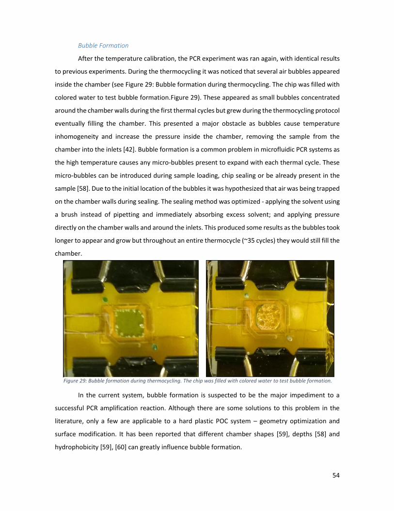
54
Bubble Formation
After the temperature calibration, the PCR experiment was ran again, with identical results
to previous experiments. During the thermocycling it was noticed that several air bubbles appeared
inside the chamber (see Figure 29: Bubble formation during thermocycling. The chip was filled with
colored water to test bubble formation.Figure 29). These appeared as small bubbles concentrated
around the chamber walls during the first thermal cycles but grew during the thermocycling protocol
eventually filling the chamber. This presented a major obstacle as bubbles cause temperature
inhomogeneity and increase the pressure inside the chamber, removing the sample from the
chamber into the inlets [42]. Bubble formation is a common problem in microfluidic PCR systems as
the high temperature causes any micro-bubbles present to expand with each thermal cycle. These
micro-bubbles can be introduced during sample loading, chip sealing or be already present in the
sample [58]. Due to the initial location of the bubbles it was hypothesized that air was being trapped
on the chamber walls during sealing. The sealing method was optimized - applying the solvent using
a brush instead of pipetting and immediately absorbing excess solvent; and applying pressure
directly on the chamber walls and around the inlets. This produced some results as the bubbles took
longer to appear and grow but throughout an entire thermocycle (~35 cycles) they would still fill the
chamber.
In the current system, bubble formation is suspected to be the major impediment to a
successful PCR amplification reaction. Although there are some solutions to this problem in the
literature, only a few are applicable to a hard plastic POC system – geometry optimization and
surface modification. It has been reported that different chamber shapes [59], depths [58] and
hydrophobicity [59], [60] can greatly influence bubble formation.
Figure 29: Bubble formation during thermocycling. The chip was filled with colored water to test bubble formation.

55
6. Conclusion
My goal with this work was to develop a way to prototype hard plastic microfluidics in a fast
and simple way. I began by identifying the methods better suited for this task, with special focus on
simplicity and similarity with industrial production methods. Hot Embossing was selected as the
basic fabrication method as it presents good reproduction quality and produces results similar to
Injection Molding with minimal optimization.
After performing some preliminary experiments with different mold fabrication methods
and Hot Embossing protocols, I defined a simple rapid prototyping protocol based on CNC Milling
and Hot Embossing for Polycarbonate microfluidics. This protocol was then optimized and tested
through the development of a microfluidic PCR chamber.
As expected, this presented many challenges and required extensive design changes
throughout the process. This allowed me to test the prototyping protocol in a demanding situation,
with specific design goals and requirements.
Overall, the main conclusion I draw from this work is that Hot Embossing is an excellent
platform for prototyping microfluidics and that it is possible to prototype microfluidic devices in
hard plastic in a laboratory setting. The developed protocol allowed for rapid fabrication of new
designs, easily producing multiple identical copies in under 8h.
POC devices have tremendous potential in the medical field. If successful, they could allow
for new paradigms of medical data acquisition, either enabling home-use monitoring or allowing for
comprehensive medical testing in resource-poor settings, for example. For this possibility to become
a reality, these devices need to be disposable and durable and at the moment this can only be
achieved using hard plastics. I expect that by having worked towards a simple and inexpensive
prototyping method for hard plastics it will be easier to produce functional POC devices with real-
world applications.

56
7. Bibliography
[1] N. Nguyen and S. Wereley, Fundamentals and applications of microfluidics, 2nd ed. ARtech, 2006, p. 497.
[2] A. Manz, N. Graber, and H. M. Widmer, “Miniaturized total chemical analysis systems: A novel concept for chemical sensing,” Sensors Actuators B Chem., vol. 1, no. 1–6, pp. 244–248, Jan. 1990.
[3] Y. Xia and G. M. Whitesides, “SOFT LITHOGRAPHY,” Annu. Rev. Mater. Sci., vol. 28, no. 1, pp. 153–184, Aug. 1998.
[4] G. M. Whitesides, E. Ostuni, S. Takayama, X. Jiang, and D. E. Ingber, “Soft lithography in biology and biochemistry.,” Annu. Rev. Biomed. Eng., vol. 3, pp. 335–73, Jan. 2001.
[5] K. Erickson and P. Wilding, “Evaluation of a novel point-of-care system, the i-STAT portable clinical analyzer,” Clin. Chem., vol. 39, no. 2, pp. 283–287, Feb. 1993.
[6] E. Sollier, C. Murray, P. Maoddi, and D. Di Carlo, “Rapid prototyping polymers for microfluidic devices and high pressure injections.,” Lab Chip, vol. 11, no. 22, pp. 3752–65, Nov. 2011.
[7] S. K. Sia and G. M. Whitesides, “Microfluidic devices fabricated in poly(dimethylsiloxane) for biological studies.,” Electrophoresis, vol. 24, no. 21, pp. 3563–76, Nov. 2003.
[8] K. Y. Lee, “Micromachining applications of a high resolution ultrathick photoresist,” J. Vac. Sci. Technol. B Microelectron. Nanom. Struct., vol. 13, no. 6, p. 3012, Nov. 1995.
[9] H. Lorenz, M. Despont, N. Fahrni, N. LaBianca, P. Renaud, and P. Vettiger, “SU-8: a low-cost negative resist for MEMS,” J. Micromechanics Microengineering, vol. 7, no. 3, pp. 121–124, Sep. 1997.
[10] A. Mata, A. J. Fleischman, and S. Roy, “Characterization of polydimethylsiloxane (PDMS) properties for biomedical micro/nanosystems.,” Biomed. Microdevices, vol. 7, no. 4, pp. 281–93, Dec. 2005.
[11] H. Wu, T. W. Odom, D. T. Chiu, and G. M. Whitesides, “Fabrication of complex three-dimensional microchannel systems in PDMS.,” J. Am. Chem. Soc., vol. 125, no. 2, pp. 554–9, Jan. 2003.
[12] U. M. Attia, S. Marson, and J. R. Alcock, “Micro-injection moulding of polymer microfluidic devices,” Microfluid. Nanofluidics, vol. 7, no. 1, pp. 1–28, Feb. 2009.
[13] J. Giboz, T. Copponnex, and P. Mélé, “Microinjection molding of thermoplastic polymers: a review,” J. Micromechanics Microengineering, vol. 17, no. 6, pp. R96–R109, Jun. 2007.

57
[14] J. Giboz, T. Copponnex, and P. Mélé, “Microinjection moulding of thermoplastic polymers : from theory to experiment,” in Proceedings of the 3rd International Conference on Multi-Material Micro Manufacture, 2007, p. 4.
[15] R. Surace and G. Trotta, “The micro injection moulding process for polymeric components manufacturing,” New Technol. – Trends, Innov. Res., 2012.
[16] C. Zhang, J. Xu, W. Ma, and W. Zheng, “PCR microfluidic devices for DNA amplification.,” Biotechnol. Adv., vol. 24, no. 3, pp. 243–84, Jan. 2006.
[17] R. K. Jena, C. Y. Yue, Y. C. Lam, and Z. Y. Wang, “High fidelity hot-embossing of COC microdevices using a one-step process without pre-annealing of polymer substrate,” Sensors Actuators B Chem., vol. 150, no. 2, pp. 692–699, Oct. 2010.
[18] E. W. Becker, W. Ehrfeld, P. Hagmann, A. Maner, and D. Münchmeyer, “Fabrication of microstructures with high aspect ratios and great structural heights by synchrotron radiation lithography, galvanoforming, and plastic moulding (LIGA process),” Microelectron. Eng., vol. 4, no. 1, pp. 35–56, May 1986.
[19] L. Peng, Y. Deng, P. Yi, and X. Lai, “Micro hot embossing of thermoplastic polymers: a review,” J. Micromechanics Microengineering, vol. 24, no. 1, p. 013001, Jan. 2014.
[20] M. Worgull, “Hot Embossing Process,” in Hot Embossing : Theory and Technology of Microreplication, 2009, pp. 137–177.
[21] Y. He, J.-Z. Fu, and Z.-C. Chen, “Optimization of control parameters in micro hot embossing,” Microsyst. Technol., vol. 14, no. 3, pp. 325–329, Dec. 2007.
[22] J.-T. Wu, S.-Y. Yang, W.-C. Deng, and W.-Y. Chang, “A novel fabrication of polymer film with tapered sub-wavelength structures for anti-reflection,” Microelectron. Eng., vol. 87, no. 10, pp. 1951–1954, Oct. 2010.
[23] Y. Guo, G. Liu, Y. Xiong, and Y. Tian, “Study of the demolding process—implications for thermal stress, adhesion and friction control,” J. Micromechanics Microengineering, vol. 17, no. 1, pp. 9–19, Jan. 2007.
[24] M. Koc and T. (Editor) Ozel, Micro-Manufacturing: Design and Manufacturing of Micro-Products. Wiley, 2011, p. 404.
[25] M. E. Dirckx, “Demolding of hot embossed polymer microstructures,” Massachusetts Institute of Technology, 2010.
[26] J. Wu and M. Gu, “Microfluidic sensing: state of the art fabrication and detection techniques.,” J. Biomed. Opt., vol. 16, no. 8, p. 080901, Aug. 2011.
[27] R. K. Jena, C. Y. Yue, Y. C. Lam, P. S. Tang, and a. Gupta, “Comparison of different molds (epoxy, polymer and silicon) for microfabrication by hot embossing technique,” Sensors Actuators B Chem., vol. 163, no. 1, pp. 233–241, Mar. 2012.
58
[28] H. Becker and U. Heim, “Hot embossing as a method for the fabrication of polymer high aspect ratio structures,” Sensors Actuators A Phys., vol. 83, no. 1–3, pp. 130–135, May 2000.
[29] M. B. Esch, S. Kapur, G. Irizarry, and V. Genova, “Influence of master fabrication techniques on the characteristics of embossed microfluidic channels.,” Lab Chip, vol. 3, no. 2, pp. 121–7, May 2003.
[30] E. Kukharenka, M. M. Farooqui, L. Grigore, and M. Kraft, “Electroplating moulds using dry film thick negative photoresist,” J. Micromechanics Microengineering, vol. 13, pp. 67–74, 2003.
[31] NiCo Form, “Microfluidic Molds, Electroformed Optics, MEMS,” 2014. [Online]. Available: http://www.nicoform.com/products/microfluidics-mems-and-optics. [Accessed: 23-Sep-2014].
[32] L. J. Kricka, P. Fortina, N. J. Panaro, P. Wilding, G. Alonso-Amigo, and H. Becker, “Fabrication of plastic microchips by hot embossing.,” Lab Chip, vol. 2, no. 1, pp. 1–4, Feb. 2002.
[33] R. Novak, N. Ranu, and R. a Mathies, “Rapid fabrication of nickel molds for prototyping embossed plastic microfluidic devices.,” Lab Chip, vol. 13, no. 8, pp. 1468–71, Apr. 2013.
[34] S.-J. Kim, H. Yang, K. Kim, Y. T. Lim, and H.-B. Pyo, “Study of SU-8 to make a Ni master-mold: Adhesion, sidewall profile, and removal.,” Electrophoresis, vol. 27, no. 16, pp. 3284–96, Aug. 2006.
[35] C. D. Joye, J. P. Calame, M. Garven, and B. Levush, “UV-LIGA microfabrication of 220 GHz sheet beam amplifier gratings with SU-8 photoresists,” J. Micromechanics Microengineering, vol. 20, no. 12, p. 125016, Dec. 2010.
[36] T. Koerner, L. Brown, R. Xie, and R. D. Oleschuk, “Epoxy resins as stamps for hot embossing of microstructures and microfluidic channels,” Sensors Actuators B Chem., vol. 107, no. 2, pp. 632–639, Jun. 2005.
[37] Y. Fan, T. Li, W.-M. Lau, and J. Yang, “A Rapid Hot-Embossing Prototyping Approach Using SU-8 Molds Coated With Metal and Antistick Coatings,” J. Microelectromechanical Syst., vol. 21, no. 4, pp. 875–881, Aug. 2012.
[38] V. N. Goral, Y.-C. Hsieh, O. N. Petzold, R. a Faris, and P. K. Yuen, “Hot embossing of plastic microfluidic devices using poly(dimethylsiloxane) molds,” J. Micromechanics Microengineering, vol. 21, no. 1, p. 017002, Jan. 2011.
[39] B. Warfield, “Basic Concepts for Beginners,” CNC Cookbook, 2010. [Online]. Available: http://www.cnccookbook.com/CCCNCMillFeedsSpeedsBasics.htm. [Accessed: 12-Sep-2014].
[40] P. Chen, “Micromilling Manufacturing for Polymeric Biochips,” 2012, pp. 63–67.

59
[41] G. Rumsby, “An introduction to PCR techniques.,” Methods Mol. Biol., vol. 324, pp. 75–89, Jan. 2006.
[42] C. Zhang and D. Xing, “Miniaturized PCR chips for nucleic acid amplification and analysis: latest advances and future trends.,” Nucleic Acids Res., vol. 35, no. 13, pp. 4223–37, Jan. 2007.
[43] C. D. Chin, S. Y. Chin, T. Laksanasopin, and S. K. Sia, “Point-of-Care Diagnostics on a Chip,” pp. 3–22, 2013.
[44] P. Belgrader, “PCR Detection of Bacteria in Seven Minutes,” Science (80-. )., vol. 284, no. 5413, pp. 449–450, Apr. 1999.
[45] J. Yang, Y. Liu, C. B. Rauch, R. L. Stevens, R. H. Liu, R. Lenigk, and P. Grodzinski, “High sensitivity PCR assay in plastic micro reactors.,” Lab Chip, vol. 2, no. 4, pp. 179–87, Nov. 2002.
[46] O. Clerc and G. Greub, “Routine use of point-of-care tests: usefulness and application in clinical microbiology.,” Clin. Microbiol. Infect., vol. 16, no. 8, pp. 1054–61, Aug. 2010.
[47] J. Wang, “Electrochemical biosensors: towards point-of-care cancer diagnostics.,” Biosens. Bioelectron., vol. 21, no. 10, pp. 1887–92, Apr. 2006.
[48] W. Wu, X. Fang, J. Kong, L. Xu, X. Jiang, and H. Chen, “A portable and integrated nucleic acid amplification microfluidic chip for identifying bacteria,” Lab Chip, vol. 12, no. 8, p. 1495, Apr. 2012.
[49] Q. Cao, M.-C. Kim, and C. Klapperich, “Plastic microfluidic chip for continuous-flow polymerase chain reaction: simulations and experiments.,” Biotechnol. J., vol. 6, no. 2, pp. 177–84, Feb. 2011.
[50] J. Kim, D. Byun, M. G. Mauk, and H. H. Bau, “A disposable, self-contained PCR chip.,” Lab Chip, vol. 9, no. 4, pp. 606–12, Feb. 2009.
[51] A. Bhattacharyya and C. M. Klapperich, “Thermoplastic microfluidic device for on-chip purification of nucleic acids for disposable diagnostics.,” Anal. Chem., vol. 78, no. 3, pp. 788–92, Feb. 2006.
[52] A. S. Rossney, C. M. Herra, G. I. Brennan, P. M. Morgan, and B. O’Connell, “Evaluation of the Xpert methicillin-resistant Staphylococcus aureus (MRSA) assay using the GeneXpert real-time PCR platform for rapid detection of MRSA from screening specimens.,” J. Clin. Microbiol., vol. 46, no. 10, pp. 3285–90, Oct. 2008.
[53] C. A. Holland and F. L. Kiechle, “Point-of-care molecular diagnostic systems--past, present and future.,” Curr. Opin. Microbiol., vol. 8, no. 5, pp. 504–9, Oct. 2005.
60
[54] M. Worgull, J.-F. Hétu, K. K. Kabanemi, and M. Heckele, “Hot embossing of microstructures: characterization of friction during demolding,” Microsyst. Technol., vol. 14, no. 6, pp. 767–773, Apr. 2008.
[55] A. Toh, Z. Wang, and Z. Wang, “Ambient hot embossing of polycarbonate, poly-methyl methacrylate and cyclic olefin copolymer for microfluidic applications,” Des. Test, Integr. …, pp. 1–4, 2009.
[56] J. Greener, W. Li, J. Ren, D. Voicu, V. Pakharenko, T. Tang, and E. Kumacheva, “Rapid, cost-efficient fabrication of microfluidic reactors in thermoplastic polymers by combining photolithography and hot embossing.,” Lab Chip, vol. 10, no. 4, pp. 522–4, Feb. 2010.
[57] L. Yi, W. Xiaodong, and Y. Fan, “Microfluidic chip made of COP (cyclo-olefin polymer) and comparion to PMMA (polymethylmethacrylate) microfluidic chip,” J. Mater. Process. Technol., vol. 208, no. 1–3, pp. 63–69, Nov. 2008.
[58] H. Gong, N. Ramalingam, L. Chen, J. Che, Q. Wang, Y. Wang, X. Yang, P. H. E. Yap, and C. H. Neo, “Microfluidic handling of PCR solution and DNA amplification on a reaction chamber array biochip.,” Biomed. Microdevices, vol. 8, no. 2, pp. 167–76, Jun. 2006.
[59] Y.-K. Cho, J. Kim, Y. Lee, Y.-A. Kim, K. Namkoong, H. Lim, K. W. Oh, S. Kim, J. Han, C. Park, Y. E. Pak, C.-S. Ki, J. R. Choi, H.-K. Myeong, and C. Ko, “Clinical evaluation of micro-scale chip-based PCR system for rapid detection of hepatitis B virus.,” Biosens. Bioelectron., vol. 21, no. 11, pp. 2161–9, May 2006.
[60] C. N. Liu, N. M. Toriello, and R. A. Mathies, “Multichannel PCR-CE microdevice for genetic analysis.,” Anal. Chem., vol. 78, no. 15, pp. 5474–9, Aug. 2006.
[61] A. San-Miguel and H. Lu, “Microfluidics as a tool for C. elegans research,” WormBook - The C. elegans Research Community, 2013. .
[62] Harvey Tool, “Harvey Tool - Miniature End Mill,” 2014. [Online]. Available: http://www.harveytool.com/secure/Content/ImagesProducts/8a63329d-4aa5-4aa1-97fb-fa28268a136a.jpg. [Accessed: 15-Sep-2014].
[63] W.-C. Jung, Y.-M. Heo, G.-S. Yoon, K.-H. Shin, S.-H. Chang, G.-H. Kim, and M.-W. Cho, “Micro Machining of Injection Mold Inserts for Fluidic Channel of Polymeric Biochips,” Sensors, vol. 7, no. 8, pp. 1643–1654, Aug. 2007.
[64] Wikipedia Contributors, “Polymerase Chain Reaction,” Wikipedia, 2014. [Online]. Available: http://en.wikipedia.org/w/index.php?title=Polymerase_chain_reaction&oldid=623800974. [Accessed: 01-Oct-2014].
[65] S. Park, Y. Zhang, S. Lin, T.-H. Wang, and S. Yang, “Advances in microfluidic PCR for point-of-care infectious disease diagnostics.,” Biotechnol. Adv., vol. 29, no. 6, pp. 830–9.

61
[66] A. Folch, “Liquid Smallness,” Picasa Album, 2000. [Online]. Available: https://picasaweb.google.com/102864211467583145284/LiquidSmallness?noredirect=1#5063034438858825346.

62
8. Annex
a) Arduino code for temperature control and thermocycling protocol
/***************************************************
This is an example for the Adafruit Thermocouple Sensor w/MAX31855K
Designed specifically to work with the Adafruit Thermocouple Sensor
----> https://www.adafruit.com/products/269
These displays use SPI to communicate, 3 pins are required to
interface
Adafruit invests time and resources providing this open source code,
please support Adafruit and open-source hardware by purchasing
products from Adafruit!
Written by Limor Fried/Ladyada for Adafruit Industries.
BSD license, all text above must be included in any redistribution
****************************************************/
#include "Adafruit_MAX31855.h"
int thermoDO1 = 8;
int thermoCS1 = 7;
int thermoCLK1 = 6;
int thermoDO2 = 5;
int thermoCS2 = 4;
int thermoCLK2 = 3;
int tec = 9;
Adafruit_MAX31855 thermocouple1(thermoCLK1, thermoCS1, thermoDO1);
Adafruit_MAX31855 thermocouple2(thermoCLK2, thermoCS2, thermoDO2);
void setup() {
Serial.begin(9600);
pinMode(tec, OUTPUT);
Serial.println("MAX31855 test");
// wait for MAX chip to stabilize
delay(500);
}
void holdTemp(int digTemp, int holdTime, String txtTemp){
int start = floor(millis()/1000);
int printTimer = floor(millis()/1000); // printTimer is a counter used to say
when to print sensor readout
int now = floor(millis()/1000);
int nowMin = floor(now/60);
int nowSec = now-(nowMin*60);
double c = thermocouple1.readCelsius();
double c2 = thermocouple2.readCelsius();
while(now - start <= holdTime){
c = thermocouple1.readCelsius();
c2 = thermocouple2.readCelsius();
if(c<digTemp){ //temp control
digitalWrite(tec, HIGH);}
else if(c>digTemp){ //temp control
digitalWrite(tec, LOW);}
if(now >= printTimer){
nowMin = floor(now/60);
nowSec = now-(nowMin*60);
Serial.print("Time: "); Serial.print("\t"); Serial.print(nowMin,DEC);
Serial.print("m"); Serial.print(nowSec,DEC); Serial.print("s");
Serial.print("\t");
63
Serial.print("Thermocouple1: "); Serial.print("\t"); Serial.print(c);
Serial.print("\t");
Serial.print("Thermocouple2: "); Serial.print("\t"); Serial.print(c2);
Serial.print("\t");
Serial.print(txtTemp); Serial.print("\n");
printTimer += 2;}
now = floor(millis()/1000);
}
}
void holdTemp2(int digTemp, int holdTime, int heatTime, int coolTime, String
txtTemp){
int start = floor(millis()/1000);
int printTimer = floor(millis()/1000); // printTimer is a counter used to say
when to print sensor readout
int now = floor(millis()/1000);
int nowMin = floor(now/60);
int nowSec = now-(nowMin*60);
double c = thermocouple1.readCelsius();
double c2 = thermocouple2.readCelsius();
while(now - start <= holdTime){
now = floor(millis()/1000);
c = thermocouple1.readCelsius();
c2 = thermocouple2.readCelsius();
if(now >= printTimer){
nowMin = floor(now/60);
nowSec = now-(nowMin*60);
Serial.print("Time: "); Serial.print("\t"); Serial.print(nowMin,DEC);
Serial.print("m"); Serial.print(nowSec,DEC); Serial.print("s");
Serial.print("\t");
Serial.print("Thermocouple1: "); Serial.print("\t"); Serial.print(c);
Serial.print("\t");
Serial.print("Thermocouple2: "); Serial.print("\t"); Serial.print(c2);
Serial.print("\t");
Serial.print(txtTemp); Serial.print("\n");
printTimer += 2;}
if(c<=digTemp){ // temp control
digitalWrite(tec, HIGH);
delay(heatTime);
digitalWrite(tec, LOW);
delay(coolTime);
// Serial.print("ON"); Serial.print("\n");
}
else if(c>digTemp){ //temp control
digitalWrite(tec, LOW);}
// Serial.print("OFF"); Serial.print("\n");
}
}
void heatTemp(int digTemp){
// digTemp = digital sensor readout values corresponding to temperature to hold
at
// Serial.print("Start heatTemp"); Serial.print("\n");
digitalWrite(tec, HIGH);
int printTimer = floor(millis()/1000);
int now = floor(millis()/1000);
int nowMin = floor(now/60);
int nowSec = now-(nowMin*60);
double c = thermocouple1.readCelsius();
double c2 = thermocouple2.readCelsius();
while(c < digTemp){ //temp control
now = floor(millis()/1000);
c = thermocouple1.readCelsius();
c2 = thermocouple2.readCelsius();
if(now >= printTimer){

64
nowMin = floor(now/60);
nowSec = now-(nowMin*60);
Serial.print("Time: "); Serial.print("\t"); Serial.print(nowMin,DEC);
Serial.print("m"); Serial.print(nowSec,DEC); Serial.print("s");
Serial.print("\t");
Serial.print("Thermocouple1: "); Serial.print("\t"); Serial.print(c);
Serial.print("\t");
// Serial.print("TC1 internal: "); Serial.print("\t"); Serial.print(thermoco
uple1.readInternal()); Serial.print("\n");
Serial.print("Thermocouple2: "); Serial.print("\t"); Serial.print(c2);
Serial.print("\n");
// Serial.print("TC2 internal: "); Serial.print("\t"); Serial.print(thermoco
uple2.readInternal()); Serial.print("\n");
printTimer += 2;}
}
}
void coolTemp(int digTemp){
// digTemp = digital sensor readout values corresponding to temperature to hold
at
// Serial.print("Start coolTemp"); Serial.print("\n");
digitalWrite(tec, LOW);
int printTimer = floor(millis()/1000);
int now = floor(millis()/1000);
int nowMin = floor(now/60);
int nowSec = now-(nowMin*60);
double c = thermocouple1.readCelsius();
double c2 = thermocouple2.readCelsius();
while(c > digTemp){ //temp control
now = floor(millis()/1000);
c = thermocouple1.readCelsius();
c2 = thermocouple2.readCelsius();
if(now >= printTimer){
nowMin = floor(now/60);
nowSec = now-(nowMin*60);
Serial.print("Time: "); Serial.print("\t"); Serial.print(nowMin,DEC);
Serial.print("m"); Serial.print(nowSec,DEC); Serial.print("s");
Serial.print("\t");
Serial.print("Thermocouple1: "); Serial.print("\t"); Serial.print(c);
Serial.print("\t");
Serial.print("Thermocouple2: "); Serial.print("\t"); Serial.print(c2);
Serial.print("\t"); Serial.print("\n");
printTimer += 2;}
}
}
void loop(){
heatTemp(92);
holdTemp(92, 15, "95");
for (int x = 0; x < 107; x++ ){
heatTemp(92);
holdTemp(92, 10, "94");
coolTemp(57.5);
heatTemp(61);
holdTemp(61, 25, "62");
}
heatTemp(72);
holdTemp(72, 30, "72");
coolTemp(30);
Serial.print("END");
while(1);
}

65
b) Excerpt of G-Code
N100 G0 G70 G90 N120 G0 G90 G54 X1.1261 Y-1.1249 N130 Z.25 N140 Z.2 N150 G1 Z-.0197 F6.42 N160 X-1.1261 N170 Y-1.0499 N180 X1.1261 N190 Y-.9749 N200 X-1.1261 N210 Y-.8999 N220 X.5601 N230 G2 X.4254 Y-.8249 I.625 J-.625 N240 G1 X-1.1261 N250 Y-.7499 N260 X.3716 N270 G2 X.347 Y-.6749 I.625 J-.625 N280 G1 X-1.1261 N290 Y-.5999 N300 X.3436 N310 G2 X.3589 Y-.5301 I.625 J-.625 N320 G1 X-.3937 N330 G2 X-.4293 Y-.525 I-.3937 J-.4051 N340 G1 X-1.1261 N350 Y-.45 N360 X-.5104 N370 G2 X-.5187 Y-.4051 I-.3937 J-.4051 N380 G1 Y-.375 N390 X-1.1261 N400 Y-.3 N410 X-.5187 N420 Y-.225 N430 X-1.1261 N440 Y-.15 N450 X-.5187 N460 Y-.075 N470 X-1.1261 N480 Y0. N490 X-.5187


