The pristine atomic structure of MoS2 monolayer protected from electron radiationdamage by grapheneGerardo Algara-Siller, Simon Kurasch, Mona Sedighi, Ossi Lehtinen, and Ute Kaiser Citation: Applied Physics Letters 103, 203107 (2013); doi: 10.1063/1.4830036 View online: http://dx.doi.org/10.1063/1.4830036 View Table of Contents: http://scitation.aip.org/content/aip/journal/apl/103/20?ver=pdfcov Published by the AIP Publishing
This article is copyrighted as indicated in the abstract. Reuse of AIP content is subject to the terms at: http://scitation.aip.org/termsconditions. Downloaded to IP:
134.60.120.222 On: Fri, 15 Nov 2013 08:45:56
The pristine atomic structure of MoS2 monolayer protected from electronradiation damage by graphene
Gerardo Algara-Siller,a) Simon Kurasch,a) Mona Sedighi, Ossi Lehtinen, and Ute Kaiserb)
Central Facility for Electron Microscopy, Group of Electron Microscopy of Materials Science,Ulm University, Germany
(Received 27 September 2013; accepted 26 October 2013; published online 13 November 2013;
publisher error corrected 14 November 2013)
Materials can, in principle, be imaged at the level of individual atoms with aberration-corrected
transmission electron microscopy. However, such resolution can be attained only with very high
electron doses. Consequently, radiation damage is often the limiting factor when characterizing
sensitive materials. Here, we demonstrate a simple and an effective method to increase the electron
radiation tolerance of materials by using graphene as protective coating. This leads to an
improvement of three orders of magnitude in the radiation tolerance of monolayer MoS2. Further
on, we construct samples in different heterostructure configurations to separate the contributions
of different radiation damage mechanisms. VC 2013 AIP Publishing LLC.
[http://dx.doi.org/10.1063/1.4830036]
Radiation damage is a prevalent challenge when materi-
als are introduced in radiation-hostile environments, either
on purpose or inadvertently, e.g., in nuclear reactors, space
applications, or scientific instruments such as in transmission
electron microscopes (TEM). Nowadays, in state of the art
TEMs, the sample is imaged using a beam of energetic elec-
trons with energies ranging from 20 keV (Refs. 1–3) to
300 keV. Hardware aberration-correction (AC) in a TEM4–6
allows—in principle—direct in-situ observation of single
atoms7 and single atomic columns8 of materials. However,
the instrumental resolution can only be reached when the
material can withstand an unlimited electron dose. In prac-
tice, this is rarely the case. Therefore, the resolution in the
high-resolution TEM image is nowadays predominantly lim-
ited by the electron dose, which the specimen can tolerate
before it is damaged.9
On the other hand, simultaneous production and obser-
vation of radiation-induced transformations in the sample
allow detailed studies of radiation damage in a TEM.
Traditionally, second-order phenomena, such as fading of
diffraction spots connected to the loss of sample crystallinity,
mass-loss, changes in the energy-loss spectra, and electron
beam induced x-ray yield, have been used for characteriza-
tion of radiation damage10 in classical three-dimensional
specimens. Two-dimensional (2D) materials, such as gra-
phene, h-BN, and MoS2, however, have allowed resolving
the electron-beam-induced changes atom-by-atom, making a
direct observation of radiation damage at the level of the ba-
sic building blocks of matter—the atoms—possible.11–14 A
notable difference in bulk materials is that in such 2D mate-
rials surface effects are dominating, as in essence, surface is
all the materials have.
Radiation damage in the TEM is divided into two differ-
ent categories, where the first one is related to displacements
of atoms through direct collisions between the energetic
electrons and target atoms (so called knock-on damage), and
the second to excitations of the electronic system of the
target,15 which can lead, e.g., to radiolysis. Moreover, energy
deposition from the electron beam can lead to heating of the
specimen and to ejection of secondary electrons. The latter
may result in a significant electrostatic charging in insulating
materials, which can even lead to a so-called Coulomb
explosion,16 where heavily charged material disintegrates
due to internal electrostatic repulsion. Contaminants on the
sample surface and residual gases in the vacuum of the
microscope can be broken down, thus creating free radicals,
which can lead to a chemical etching of the sample surface.17
Interplay of damage mechanisms is possible, e.g., if the
response of the target to knock-on collisions is different in
an electronically excited or charged state. Theoretical predic-
tions of radiation damage in the TEM have been limited
mostly to the simplest case of the knock-on process12–14
since calculations on the other processes are considerably
more challenging.
Many approaches have been proposed and employed for
combating the adverse effects of electron radiation. On the
instrumentation side, lowering the electron energy reduces
knock-on damage, as there is a material specific threshold in
momentum, which needs to be transferred to the target atom
in order to displace it from its lattice position. The cost of a
lower electron energy, however, is loss in attainable resolu-
tion, and thus the aim is to work below, but close to the dam-
age threshold energy. On the other hand, increasing the
electron energy lowers the inelastic scattering cross-section,
thus reducing damage related to the excitations of the elec-
tronic system of the target. Depending on which mechanism
is predominant in a sample, an optimal electron energy needs
to be selected.1,15
An alternative route for combating radiation damage is
treatment of the sample itself. Protecting a specimen by coat-
ing it with conducting and/or radiation resistant material is a
well established method.17 Such coating can serve as a
source of electrons, which can compensate the charging
effect in the sample, serve as a thermal conductor, and/or
protect the sample from chemical etching.18 Further on,
a)G. Algara-Siller and S. Kurasch contributed equally to this work.b)Electronic mail: [email protected]
0003-6951/2013/103(20)/203107/5/$30.00 VC 2013 AIP Publishing LLC103, 203107-1
APPLIED PHYSICS LETTERS 103, 203107 (2013)
This article is copyrighted as indicated in the abstract. Reuse of AIP content is subject to the terms at: http://scitation.aip.org/termsconditions. Downloaded to IP:
134.60.120.222 On: Fri, 15 Nov 2013 08:45:56
when the exit surface of the sample is coated, sputtering of
target material can be inhibited. As an extreme demonstra-
tion of the benefits of coating a sample, mosquito larvae
were recently demonstrated to come out alive and even hatch
after investigation in the vacuum of a scanning electron
microscope when a coating treatment was applied.19
A typical drawback of coating a specimen, however, is
that it obscures the specimen itself, degrades the signal to
noise ratio, and consequently reduces the attainable speci-
men resolution. Therefore, an optimal coating material
would have excellent electrical and thermal conductivity, be
resistant and highly transparent to electrons at the used
energy, be chemically inert, and be crystalline. The last is
important as the known image contribution of the crystalline
lattice can be removed from the micrographs in digital
post-processing, e.g., by Fourier filtering.20,21 The material
meeting all these criteria is graphene, and it has indeed been
suggested and employed as the ultimate sample substrate for
TEM.1,7,18,20,22–28,37 The usefulness of graphene in reducing
ion radiation damage has been reported in other studies,
where significant reduction in the sputtering yield of plati-
num covered with graphene under ion irradiation has been
predicted,29 and reduced damage in graphene sandwiched
between SiO2 and another graphene layer under ion bom-
bardment has been observed.30
In this study, we show how coating an electron beam
sensitive material—single layer MoS2—with graphene
dramatically improves its electron radiation resistance. We
analyse the evolution of the electron radiation damage at
atomic resolution, employing 80 kV AC-HRTEM. We show
that the electron radiation resistance of the MoS2 single layer
is increased by nearly three orders of magnitude when it is
sandwiched between two graphene layers, as compared to
the free standing MoS2 layer (see Fig. 1). This demonstrates
the effectiveness of our graphene-sandwich-approach in
fighting radiation damage. In addition, by preparing samples
in different heterostructure configurations, we are able to
separate the role of the different damage mechanisms in the
material at the level of single atoms.
For this purpose, we constructed samples in four
different configurations, using the following procedure: A
graphene flake (1–3 layers) was mechanically exfoliated
from graphite, deposited on SiO2(90 nm)/Si, and transferred
to Quantifoil grids using KOH.31 Single layer MoS2 was also
cleaved from a natural crystal, and deposited on SiO2/Si. In
order to transfer the MoS2 flake to the already transferred
graphene, we positioned the graphene/Quantifoil on the top
of the single layer MoS2. Once positioned, the MoS2 layer
was transferred via the same method as used for graphene.
This process was repeated for another graphene layer. As a
result, we got a sandwich structure, where the MoS2 layer
lays in between graphene layers. The HRTEM investigations
were performed in an aberration-corrected FEI TITAN
80-300 operated at 80 kV with Cs¼ 0.03 mm under Scherzer
conditions. The vacuum level in the microscope was
<10�7 millibars.
As the baseline sample, we used a free-standing MoS2,
which was also the subject of an earlier study.14 For evaluat-
ing the ultimate protective power of the graphene layers, the
sandwich structure was constructed (named the G/MoS2/G
configuration), where the MoS2 layer was enclosed between
graphene layers via subsequent transfer of the mechanically
exfoliated layers on to a TEM grid at the same position
(see Fig. 1(a) for a schematic representation). For separating
the effects of the different damage mechanisms, two hetero-
structures with MoS2 monolayer and graphene were con-
structed, with graphene either on top or bottom of the MoS2
layer (named the G/MoS2 and MoS2/G configurations).
Based on light-micrographs produced during sample
preparation, the correct sample area was located at low mag-
nification in the TEM in order to minimize the electron dose
before the characterization of the effects of the electron beam
on the material. Electron diffraction patterns were recorded
for verifying the monolayer nature of the MoS232 at the area
under investigation. A diffractogram of the G/MoS2/G sam-
ple is presented in Fig. 1(b), showing the two graphene peaks
originating from the top and bottom layers, and the peaks of
alternating intensity from the MoS2 monolayer.
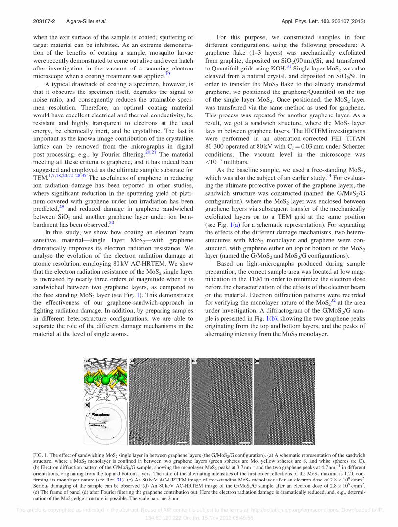
FIG. 1. The effect of sandwiching MoS2 single layer in between graphene layers (the G/MoS2/G configuration). (a) A schematic representation of the sandwich
structure, where a MoS2 monolayer is confined in between two graphene layers (green spheres are Mo, yellow spheres are S, and white spheres are C).
(b) Electron diffraction pattern of the G/MoS2/G sample, showing the monolayer MoS2 peaks at 3.7 nm–1 and the two graphene peaks at 4.7 nm�1 in different
orientations, originating from the top and bottom layers. The ratio of the alternating intensities of the first-order reflections of the MoS2 maxima is 1.20, con-
firming its monolayer nature (see Ref. 31). (c) An 80 keV AC-HRTEM image of free-standing MoS2 monolayer after an electron dose of 2.8� 108 e/nm2.
Serious damaging of the sample can be observed. (d) An 80 keV AC-HRTEM image of the G/MoS2/G sample after an electron dose of 2.8� 108 e/nm2.
(e) The frame of panel (d) after Fourier filtering the graphene contribution out. Here the electron radiation damage is dramatically reduced, and, e.g., determi-
nation of the MoS2 edge structure is possible. The scale bars are 2 nm.
203107-2 Algara-Siller et al. Appl. Phys. Lett. 103, 203107 (2013)
This article is copyrighted as indicated in the abstract. Reuse of AIP content is subject to the terms at: http://scitation.aip.org/termsconditions. Downloaded to IP:
134.60.120.222 On: Fri, 15 Nov 2013 08:45:56
Once the correct sample area was located, the material
was observed in the high-resolution mode, while keeping
track of the total accumulated electron dose. All the samples
were investigated in similar conditions in terms of vacuum
level, dose rate, magnification, and total beam current.
Importantly, atomically clean areas were found in the hetero-
structure areas, which corroborate the earlier observation by
Haigh et al.33 There interfaces in similar heterostructures
were found to be contamination free, and in full contact in
cross-sectional images. Similar to what was observed in our
earlier study,14 exclusively sulphur vacancies are created
under the electron beam. By observing the rate at which the
vacancy concentration increases, one can directly evaluate
the total vacancy production cross-section in each case.
The dramatic effect of the graphene layers in the
G/MoS2/G sample can be seen when panels 1(c) and 1(d) are
compared. In panel (c), the free-standing MoS2 sample is
seriously damaged after an electron dose of 2.8� 108 e/nm2,
and the vacancies have partly rearranged into lines, as
described in Ref. 34. Consequently, no information on the
atomic structure of the pristine state of the sample can be
extracted. With G/MoS2/G sample (panel (d)), the situation
is completely different after the same electron dose. Here,
for example, the structure of the MoS2 flake edge can be
readily observed at atomic resolution, which would not be
possible with the unprotected sample, and the vacancy con-
centration in the flake remains very low. Panel (e) shows the
same HRTEM frame as in panel (d), but after filtering out
the graphene contribution and high frequency noise by
means of Fourier filtering, which further improves the inter-
pretability of the MoS2 structure by removing the Moir�eeffect resulting from the overlay of the MoS2 and the gra-
phene lattices.
For quantifying the damage rate and for studying the
contributions of the different damage mechanisms, all the
four samples were given an electron dose at which the va-
cancy concentration increased up to 4%, and HRTEM
images before and after the irradiation were compared, tak-
ing account of the increase in vacancy concentration. The
relevant measured quantities are given in Table I, along with
the calculated vacancy production cross-sections. The cross-
sections are calculated by r ¼ DN=ðN/Þ, where DN is the
number of lost S atoms, N is the total number of S sites in
the investigated area, and / is the accumulated electron
dose.
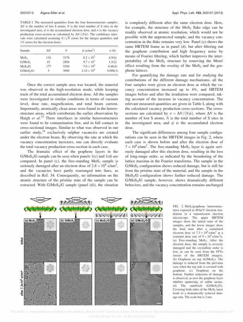
The significant differences among four sample configu-
rations can be seen in the HRTEM images in Fig. 2, where
each case is shown before and after the electron dose of
7� 108 e/nm2. The free-standing MoS2 layer is again seri-
ously damaged after this electron dose, resulting in the loss
of long-range order, as indicated by the broadening of the
lattice maxima in the Fourier transforms. The sample in the
G/MoS2 configuration shows reduced damage, but is still far
from the pristine state of the material, and the sample in the
MoS2/G configuration shows further reduced damage. The
G/MoS2/G sample, however, shows dramatically different
behaviors, and the vacancy concentration remains unchanged
TABLE I. The measured quantities from the four heterostructure samples.
DN is the number of lost S atoms, N is the total number of S sites in the
investigated area, / is the accumulated electron dose, and r is the vacancy
production cross-section as calculated by DN=ðN/Þ. The confidence inter-
vals were calculated assuming N=ffiffiffiffi
Np
errors for the integer quantities and
1% errors for the electron doses.
Sample DN N / (e/nm2) r (b)
MoS2 116 3176 8.2� 107 4.5(4)
G/MoS2 43 2894 9.7� 107 1.5(2)
MoS2/G 177 5294 7.0� 108 0.48(4)
G/MoS2/G 5 3090 2.14� 109 0.008(3)
FIG. 2. MoS2/graphene heterostruc-
tures exposed to 80 keV electron irra-
diation in a transmission electron
microscope. The upper HRTEM
images show the initial state of the
samples, and the lower images show
the final state after a cumulated
electron dose of 7.3� 108 e/nm2 at a
constant dose rate of 9� 105 e/nm2/s.
(a) Free-standing MoS2. After the
electron dose, the sample is severely
damaged and the crystalline order is
lost, as can be seen from the FFTs
(insets of the HRTEM images).
(b) Graphene on top (G/MoS2). The
damage is reduced from the previous
case when the top side is covered with
graphene. (c) Graphene on the
bottom. Further reduction of damage
is observed, as now the graphene layer
inhibits sputtering of sulfur atoms.
(d) The sandwich (G/MoS2/G).
Covering both sides of the MoS2 layer
leads to a dramatically reduced dam-
age rate. The scale bar is 2 nm.
203107-3 Algara-Siller et al. Appl. Phys. Lett. 103, 203107 (2013)
This article is copyrighted as indicated in the abstract. Reuse of AIP content is subject to the terms at: http://scitation.aip.org/termsconditions. Downloaded to IP:
134.60.120.222 On: Fri, 15 Nov 2013 08:45:56
after the electron dose, which completely destroyed the
free-standing target. We would like to point out that we do
see occasional migration steps of vacancies also in the
G/MoS2/G configuration (the locations of the vacancies in
the G/MoS2/G frames in Fig. 2 are not identical). See supple-
mentary material35 for a further demonstration of the differ-
ence between damage rates in the G/MoS2/G and the
G/MoS2 configurations, where a spot in the G/MoS2/G sam-
ple was located, at which the bottom graphene layer ends,
thus allowing the observation and comparison of fully and
half covered parts at the exact same conditions.
The cross-sections for the MoS2, G/MoS2, MoS2/G, and
G/MoS2/G configurations were determined to be 4.5(4) b,
1.5(2) b, 0.48(4) b, and 0.008(3) b, respectively, (1 b equals
10�10 nm2, the number in parenthesis denotes the one sigma
confidence interval of the last digit/digits). As compared to the
free-standing case, the cross-section is reduced by a factor of
2.9 for the G/MoS2 configuration, 9.3 for the MoS2/G configu-
ration and 600 for the G/MoS2/G configuration. If one
defines the critical electron dose to be the dose at which 5%
of target sulphur atoms are lost, one gets values of
1.12(11)� 108 e/nm2, 3.3(5)� 108 e/nm2, 1.05(8)� 109 e/nm2,
and 6(3)� 1010 e/nm2 for the MoS2, G/MoS2, MoS2/G, and
G/MoS2/G configurations, respectively. Quantification of dam-
age in the graphene layers is not possible due to the much
stronger contrast originating from the MoS2 layer. However,
prior studies have shown that graphene is quite robust under
80 keV electron beam and tends to flexibly reorganize into a
closed network in the presence of vacancy type defects.12,36
By comparing the samples in the G/MoS2 and MoS2/G
configurations, it can immediately be seen that knock-on
damage is not the dominant damage mechanism in MoS2
under the electron beam, contrary to what was assumed in
our earlier paper.14 Due to standard collision kinetics, the
sample atoms are always displaced away from the beam exit
surface of the sample, and the graphene layer on the exit sur-
face inhibits their ejection. If suppression of knock-on dam-
age is taken to be the only difference between the two
configurations, one can estimate the contribution of the
knock-on process by simple subtraction of the two
cross-sections. A value of 1.1(2) b is acquired, which is only
24% of the total damage cross-section in the free-standing
case and consequently, 76% of the damage is of a different
origin. This knock-on cross-section is in good agreement
with the theoretical prediction of 0.8 b.14 It should be pointed
out that the theoretical value is based on a displacement
threshold calculated specifically for sulphurs in the bottom
layer, which is easier to displace than the top layer sulphurs.
Comparison of the samples with only single side covered
and the free-standing MoS2 sample allows studying the
effects of the other damage mechanisms, although clearly iso-
lating the mechanisms is not as straight-forward as in the case
of knock-on damage. If one assumes that already covering a
single side of the MoS2 layer with graphene suppresses the
damage processes caused by electronic excitations and charg-
ing, and thus only chemical etching on one surface is active
in the MoS2/G configuration, one can further calculate a
cross-section of 2.4(6) b as the contribution related to elec-
tronic excitations and charging (55% of the free-standing
cross-section). This number, however, should be taken as a
rough estimate. In future experiments, it would be of great in-
terest to replace the graphene layer on one or both surfaces by
a hexagonal boron-nitride layer, which is chemically inert,
has comparable mechanical properties to those of graphene,
but is an insulating material. Such samples would allow fur-
ther separation of the different damage mechanisms.
To conclude, we have applied graphene as a coating ma-
terial for dramatically reducing radiation damage in single
layer MoS2 induced by the 80 keV electrons used for
high-resolution imaging in AC-HRTEM. Our sample prepa-
ration method allows characterization of the pristine atomic
structure of a radiation sensitive material. Moreover, we dem-
onstrated the usefulness of different layered graphene-MoS2
heterostructures in separating different radiation damage
mechanisms. The technological implications are obvious:
Using graphene as a protective layer is highly advantageous
when imaging radiation sensitive materials in a transmission
electron microscope, from thin layers to isolated molecules.
This expands the applicability of the AC-HRTEM signifi-
cantly, as radiation damage has been a serious hindrance in
fully exploiting the greatly improved resolving power of
the aberration-corrected instrument. The total vacancy crea-
tion cross-section was reduced 600 fold going from a
free-standing MoS2 layer (4.5(4) b) to the sandwiched config-
uration (0.008(3) b). The contribution of knock-on damage
was separated from the total damage cross-section (1.1(2) b),
and was observed to only partially explain the total accumu-
lated damage. An estimate on the cross-section related to
electronic excitations was deduced (2.4(6) b), although heter-
ostructures of different materials would be useful in address-
ing this effect more reliably. Other types of displacing
radiation were not explicitly studied here, but our results sug-
gest that graphene can be used also more generally in protect-
ing surfaces from radiation damage.
Note Added in Proof: During the reviewing of this work, it
has come to our attention that R. Zan et al. have recently and
independently reported similar results to ours, but using
focused beam scanning TEM37 instead of broad illumination
TEM.
The authors acknowledge the financial support by the
DFG (German Research Foundation) and the Ministry of
Science, Research and the Arts (MWK) of Baden-
Wuerttemberg in the frame of the SALVE (Sub Angstrom
Low-Voltage Electron microscopy) project. O.L. acknowl-
edges financial support from the Finnish Cultural Foundation.
The authors thank Dr. A. V. Krasheninnikov and Dr. H.-P.
Komsa for helpful discussions.
Author Contributions: G.A.S., S.K., and U.K. conceived
and planned the experiments. M.S. prepared the samples
under the supervision of G.A.S., and S.K. S.K. executed the
HRTEM imaging under the supervision of U.K. All the
authors contributed to the analysis of the data. O.L. wrote
the manuscript with assistance from U.K. and all the authors.
1U. Kaiser, J. Biskupek, J. Meyer, J. Leschner, L. Lechner, H. Rose, M.
St€oger-Pollach, A. Khlobystov, P. Hartel, H. M€uller, M. Haider, S.
Eyhusen, and G. Benner, Ultramicroscopy 111, 1239 (2011).
203107-4 Algara-Siller et al. Appl. Phys. Lett. 103, 203107 (2013)
This article is copyrighted as indicated in the abstract. Reuse of AIP content is subject to the terms at: http://scitation.aip.org/termsconditions. Downloaded to IP:
134.60.120.222 On: Fri, 15 Nov 2013 08:45:56
2H. Sawada, T. Sasaki, F. Hosokawa, S. Yuasa, M. Terao, M. Kawazoe, T.
Nakamichi, T. Kaneyama, Y. Kondo, K. Kimoto, and K. Suenaga,
Ultramicroscopy 110, 958 (2010).3O. L. Krivanek, N. Dellby, M. F. Murfitt, M. F. Chisholm, T. J. Pennycook, K.
Suenaga, and V. Nicolosi, Ultramicroscopy 110, 935 (2010).4M. Haider, H. Rose, S. Uhlemann, E. Schwan, B. Kabius, and K. Urban,
Ultramicroscopy 75, 53 (1998).5O. Krivanek, N. Dellby, and A. Lupini, Ultramicroscopy 78, 1 (1999).6B. Kabius, P. Hartel, M. Haider, H. M€uller, S. Uhlemann, U. Loebau,
J. Zach, and H. Rose, J. Electron Microsc. 58, 147 (2009).7J. C. Meyer, C. O. Girit, M. F. Crommie, and A. Zettl, Nature 454, 319
(2008).8C. L. Jia, M. Lentzen, and K. Urban, Science 299, 870 (2003).9H. H. Rose, Philos. Trans. R. Soc. London, Ser. A 367, 3809 (2009).
10L. Reimer, Ultramicroscopy 14, 291 (1984).11F. Banhart, J. Kotakoski, and A. V. Krasheninnikov, ACS Nano 5, 26
(2011).12J. Kotakoski, A. V. Krasheninnikov, U. Kaiser, and J. Meyer, Phys. Rev.
Lett. 106, 105505 (2011).13J. C. Meyer, F. Eder, S. Kurasch, V. Skakalova, J. Kotakoski, H. J. Park,
S. Roth, A. Chuvilin, S. Eyhusen, G. Benner, A. V. Krasheninnikov, and
U. Kaiser, Phys. Rev. Lett. 108, 196102 (2012).14H.-P. Komsa, J. Kotakoski, S. Kurasch, O. Lehtinen, U. Kaiser, and A. V.
Krasheninnikov, Phys. Rev. Lett. 109, 035503 (2012).15R. Egerton, P. Li, and M. Malac, Micron 35, 399 (2004).16X. Wei, D.-M. Tang, Q. Chen, Y. Bando, and D. Golberg, ACS Nano 7,
3491 (2013).17L. Reimer and H. Kohl, Transmission Electron Microscopy (Springer
ScienceþBusiness Media, 2008).18J. M. Yuk, J. Park, P. Ercius, K. Kim, D. J. Hellebusch, M. F. Crommie,
J. Y. Lee, A. Zettl, and A. P. Alivisatos, Science 336, 61 (2012).19Y. Takaku, H. Suzuki, I. Ohta, D. Ishii, Y. Muranaka, M. Shimomura, and
T. Hariyama, Proc. Natl. Acad. Sci. U.S.A. 110, 7631 (2013).20Z. Lee, K.-J. Jeon, A. Dato, R. Erni, T. J. Richardson, M. Frenklach, and
V. Radmilovic, Nano Lett. 9, 3365 (2009).21B. Westenfelder, J. C. Meyer, J. Biskupek, S. Kurasch, F. Scholz, C. E.
Krill, and U. Kaiser, Nano Lett. 11, 5123 (2011).
22J.-N. Longchamp, T. Latychevskaia, C. Escher, and H.-W. Fink, Appl.
Phys. Lett. 101, 113117 (2012).23B. Westenfelder, J. C. Meyer, J. Biskupek, G. Algara-Siller, L. G.
Lechner, J. Kusterer, U. Kaiser, C. E. Kril III, E. Kohn, and F. Scholz,
J. Phys. D: Appl. Phys. 44, 055502 (2011).24R. S. Pantelic, J. W. Suk, C. W. Magnuson, J. C. Meyer, P.
Wachsmuth, U. Kaiser, R. S. Ruoff, and H. Stahlberg, J. Struct. Biol.
174, 234 (2011).25R. R. Nair, P. Blake, J. R. Blake, R. Zan, S. Anissimova, U. Bangert, A. P.
Golovanov, S. V. Morozov, A. K. Geim, K. S. Novoselov, and T.
Latychevskaia, Appl. Phys. Lett. 97, 153102 (2010).26R. S. Pantelic, J. C. Meyer, U. Kaiser, and H. Stahlberg, Solid State
Commun. 152, 1375 (2012).27J. Lee, K. S. Novoselov, and H. S. Shin, ACS Nano 5, 608 (2011).28J. H. Warner, M. H. R€ummeli, A. Bachmatiuk, M. Wilson, and B.
B€uchner, ACS Nano 4, 470 (2010).29S. Standop, O. Lehtinen, C. Herbig, G. Lewes-Malandrakis, F. Craes, J.
Kotakoski, T. Michely, A. V. Krasheninnikov, and C. Busse, Nano Lett.
13, 1948 (2013).30M. Kalbac, O. Lehtinen, A. V. Krasheninnikov, and J. Keinonen, Adv.
Mater. 25, 1004 (2013).31J. C. Meyer, C. O. Girit, M. F. Crommie, and A. Zettl, Appl. Phys. Lett.
92, 123110 (2008).32J. Brivio, D. T. L. Alexander, and A. Kis, Nano Lett. 11, 5148 (2011).33S. J. Haigh, A. Gholinia, R. Jalil, S. Romani, L. Britnell, D. C. Elias, K. S.
Novoselov, L. A. Ponomarenko, A. K. Geim, and R. Gorbachev, Nature
Mater. 11, 764 (2012).34H.-P. Komsa, S. Kurasch, O. Lehtinen, U. Kaiser, and A. V.
Krasheninnikov, Phys. Rev. B 88, 035301 (2013).35See supplementary material at http://dx.doi.org/10.1063/1.4830036 for a
demonstration of different damage rates at the interface of G/MoS2 and
G/MoS2/G.36O. Lehtinen, S. Kurasch, A. V. Krasheninnikov, and U. Kaiser, Nat.
Commun. 4, 2098 (2013).37R. Zan, Q. M. Ramasse, R. Jalil, T. Georgiou, U. Bangert, and K. S.
Novoselov, “Control of radiation damage in MoS2 by graphene
encapsulation,” ACS Nano (published online).
203107-5 Algara-Siller et al. Appl. Phys. Lett. 103, 203107 (2013)
This article is copyrighted as indicated in the abstract. Reuse of AIP content is subject to the terms at: http://scitation.aip.org/termsconditions. Downloaded to IP:
134.60.120.222 On: Fri, 15 Nov 2013 08:45:56


