System and SoC Verification Trends
Nick Heaton, Senior Solution Architect
Verification Futures
19th Nov (Windsor), 21st Nov (Grenoble), 22nd Nov (Munich)
2 © 2012 Cadence Design Systems, Inc. All rights reserved.
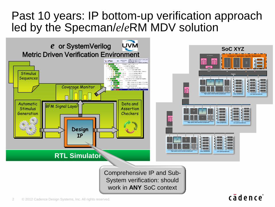
Past 10 years: IP bottom-up verification approach led by the Specman/e/eRM MDV solution
Metric Driven Verification Environment
Automatic Stimulus
Generation
Data and Assertion Checkers
BFM Signal Layer
Coverage Monitor
Stimulus Sequences
Customer’s Application Specific Components CPU subsystem
3
D
Gr
ap
hi
cs
C
or
e
D
S
P
A/
V
High speed, wired interface peripherals
D
D
R
3
P
H
Y
Other peripherals
S
A
T
A MI
PI
H
D
MI
W
L
A
N L
T
E
Low-speed peripheral
subsystem
Low speed peripherals
P
M
U M
I
P
I J
T
A
G
I
N
T
C I
2
C S
P
I T
i
m
e
r
G
P
I
O
D
i
s
p
l
a
y
U
A
R
T
Applica
tion
Acceler
ators
…
A
E
S
…
Fabric
CPU
I $
D $
CPU
I $
D $
L2 cache
USB3.0
3
.
0
P
H
Y
2
.
0
P
H
Y
PCIe
Gen
2,3
PHY
E
t
h
e
r
-
n
e
t
P
H
Y
Customer’s Application Specific Components CPU subsystem
3
D
Gr
ap
hi
cs
C
or
e
D
S
P
A/
V
High speed, wired interface peripherals
D
D
R
3
P
H
Y
Other peripherals
S
A
T
A MI
PI
H
D
MI
W
L
A
N L
T
E
Low-speed peripheral
subsystem
Low speed peripherals
P
M
U M
I
P
I J
T
A
G
I
N
T
C I
2
C S
P
I T
i
m
e
r
G
P
I
O
D
i
s
p
l
a
y
U
A
R
T
Applica
tion
Acceler
ators
…
A
E
S
…
Fabric
CPU
I $
D $
CPU
I $
D $
L2 cache
USB3
.0
3
.
0
P
H
Y
2
.
0
P
H
Y
PCIe Gen 2,3
PHY
E
t
h
e
r
-
n
e
t
P
H
Y
Customer’s Application Specific Components CPU subsystem
3
D
Gr
ap
hi
cs
C
or
e
D
S
P
A/
V
High speed, wired interface peripherals
D
D
R
3
P
H
Y
Other peripherals
S
A
T
A MI
PI
H
D
MI
W
L
A
N L
T
E
Low-speed peripheral
subsystem
Low speed peripherals
P
M
U M
I
P
I J
T
A
G
I
N
T
C I
2
C S
P
I T
i
m
e
r
G
P
I
O
D
i
s
p
l
a
y
U
A
R
T
Applica
tion
Acceler
ators
…
A
E
S
…
Fabric
CPU
I $
D $
CPU I $
D $
L2 cache
USB3.0
3
.
0
P
H
Y
2
.
0
P
H
Y
PCIe Gen 2,3
PHY
E
t
h
e
r
-
n
e
t
P
H
Y
SoC XYZ
Design IP
e or SystemVerilog
RTL Simulator
Comprehensive IP and Sub-
System verification: should
work in ANY SoC context

3 © 2012 Cadence Design Systems, Inc. All rights reserved.
Paradigm Shift In the Market
Ubiquity of software
Move to Standards-based protocols and IPs
Increasing complexity and # of IP’s to be integrated
Application / end-user driven requirements
Shrinking time-to-money
Mixed Signal and Low Power Verification Complexity
Debug consuming over 50% of verification task
Design
Trends
Shift from:
Serial HW/SW
Development
To:
Parallel HW/SW
Development
Shift from:
IP Creation
To:
SoC Integration

Debug is a Major Bottleneck in Verification
4
• Customers spending >50% verification effort in Debug
• Verification complexity requires advanced class and macro debug
• Debug methodology shift from signals Class / Transactions
50%
Verification
efforts
5% 10%
25%
10% Test planning
Test creation
Test execution (formal + sim + HW)
Debug
Coverage analysis

5 © 2012 Cadence Design Systems, Inc. All rights reserved.
From serial to parallel HW/SW development
Block Chip Prototype Silicon
lab test Field test
ROM
Content Drivers / RTOS / Applications
Diagnostics
& Firmware HW/SW
Spec
Serial HW->SW Development
Block Chip Prototype Silicon
lab test Field test
ROM
Content Drivers / RTOS / Applications
Diagnostics
& Firmware HW/SW
Spec
Time to market
advantage of 6 to
9 months
Parallel HW->SW Development
Integrate HW/SW Early and Often
HW designed in SW context
Software exposed to Spec changes
6 © 2012 Cadence Design Systems, Inc. All rights reserved.
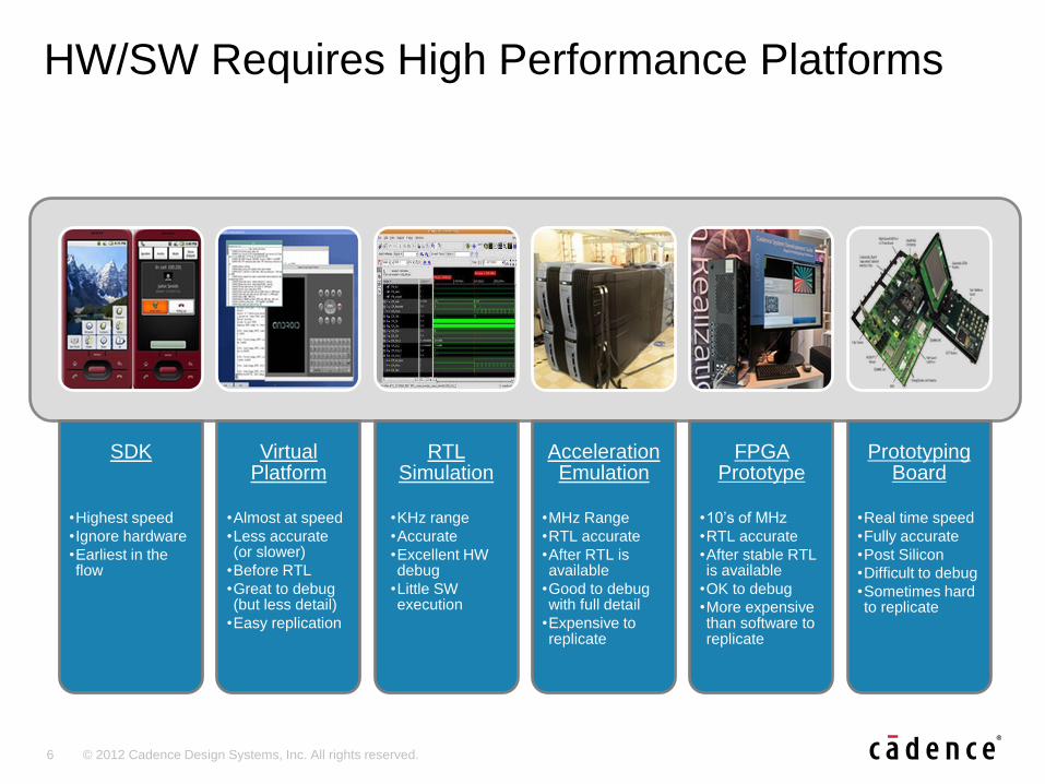
HW/SW Requires High Performance Platforms
SDK
•Highest speed
•Ignore hardware
•Earliest in the flow
Virtual Platform
•Almost at speed
•Less accurate (or slower)
•Before RTL
•Great to debug (but less detail)
•Easy replication
RTL Simulation
•KHz range
•Accurate
•Excellent HW debug
•Little SW execution
Acceleration Emulation
•MHz Range
•RTL accurate
•After RTL is available
•Good to debug with full detail
•Expensive to replicate
FPGA Prototype
•10’s of MHz
•RTL accurate
•After stable RTL is available
•OK to debug
•More expensive than software to replicate
Prototyping Board
•Real time speed
•Fully accurate
•Post Silicon
•Difficult to debug
•Sometimes hard to replicate
7 © 2012 Cadence Design Systems, Inc. All rights reserved.
• Multiple disconnected SoC simulation environments – Virtual Platform, RTL Sim, HW Acceleration/Emulation, FPGA
Prototype, Post Silicon
• Reducing SoC integration time and effort – Integrating many design IPs and SW components
– Requires significant time and effort to verify integration
– High cost to re-integrate & re-verify changes
– Debug is a major challenge to isolate the root cause
– Verification effort for SoC derivatives is too high
• Verifying that SoC can support required SW applications – Increased software content to develop, integrate, & verify
– SoC must be architected up front to support SW Use Cases
– Must verify against functional, power & performance requirements
Main Challenges Integrating and Verifying Large-Scale Multicore SoCs
8 © 2012 Cadence Design Systems, Inc. All rights reserved.
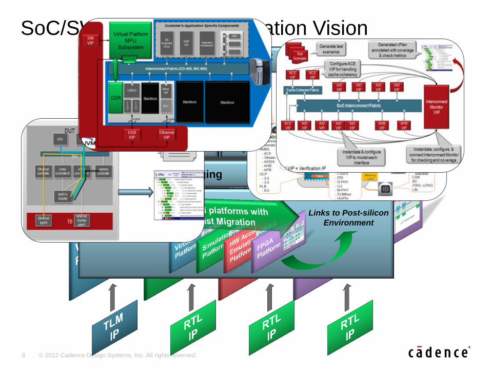
SoC/SW Integration Verification Vision
System
Development
Suite
Links to Post-silicon
Environment
System Integration Automation
Application-Driven System Verification
Verification Planning & Management
System VIP
Simulation
VIP
Accelerated
VIP
Speed
Bridge
Virtual
Bridge
Unified System Debugging
9 © 2012 Cadence Design Systems, Inc. All rights reserved.


