
Survival of VLSI design – coping with device variability and uncertaintyKevin NowkaSr Mgr VLSI SystemsIBM Austin Research Laboratory
Acknowledgements:Sani Nassif, Anne Gattiker (IBM Austin Research)Chandu Visweswariah, David Frank (IBM Watson Research), Lars Liebmann, Dan Maynard (IBM Server & Technology Group)

Slide 2Texas A&M 23 Oct 2007
Motivation for overcoming variation (or at least coping)?
What is at stake? The VLSI economy
Using greaterthan 10k ofthese..
to make these..
to make these..
to make these..
Very Large Scale Integration is:

Slide 3Texas A&M 23 Oct 2007
The VLSI Economy
1900 1920 1940 1960 1980 2000 2020
MechanicalElectro-mechanical
Vacuum tubeDiscrete transistor
Integrated circuit
Year
1,000,000,000,000
1,000,000,000
1,000,000
1,000
1
0.001
0.000001
Com
puta
tions
/ se
c
after Kurzweil, 1999 & Moravec, 1998
What $1000 buys
VLSI era6-orders magnitude
Oct 1981IBM PC8088 CPU, 64K RAM, 160K floppy drivelist price $2,880.

Slide 4Texas A&M 23 Oct 2007
The Secrets to this Success
Resilient CMOS VLSI Devices & InterconnectSimple Design Processes
Physical Abstraction with small number of rulesSimple design and design migrationComposable designs
Functional AbstractionResulting predictable functional & timing behavior
Cell-based design, place & route, static timing
Scaled Lithography (and Manufacturing Process Improvements)
Lithography improvements and the application of Dennard Scaling Rules enabling Moore’s Law

Slide 5Texas A&M 23 Oct 2007
65nm technology and beyond
Is the VLSI Economy in jeopardy because of “variability?”
What is variability?What are the important sources of variability?What are the effects on VLSI design?How are fundamental design processes impacted?How can we cope?

Slide 6Texas A&M 23 Oct 2007
What is “variability”
Intending to build this….
And sometimes (or someplaces) getting this..
And sometime (or some places) getting this

Slide 7Texas A&M 23 Oct 2007
Variability and UncertaintyVariability: known quantitative relationship between design behavior (eg. current, delay, power, noise-margin, leakage, …) and a source
Relationship can be accurately modeled, simulated, and compensated.eg. Conductor thickness as function of interconnect density.
Uncertainty: sources unknown or model too difficult/costly to generate or simulate
must be “budgeted” with some type of worst case analysiseg. Vt as a function of dopant dose and placement
Lack of modeling resources often transforms variability to uncertainty.
eg: deterministic circuit switching activity factor
Slide 8Texas A&M 23 Oct 2007
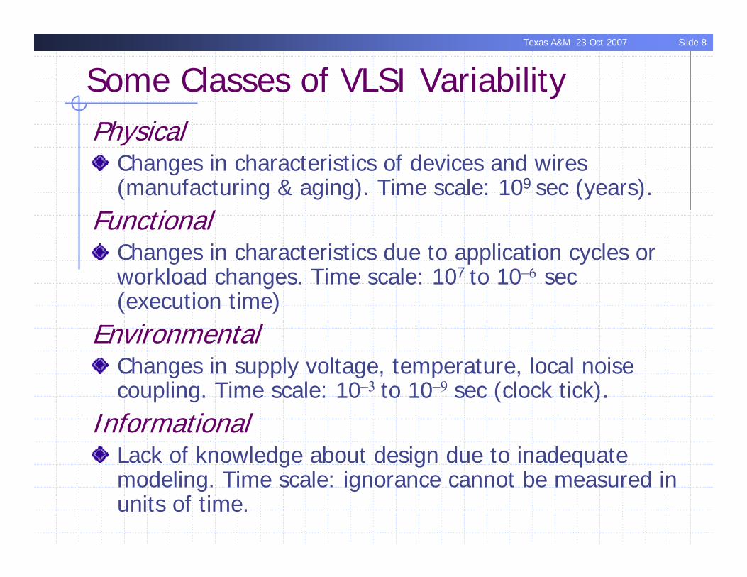
Some Classes of VLSI VariabilityPhysical
Changes in characteristics of devices and wires (manufacturing & aging). Time scale: 109 sec (years).
FunctionalChanges in characteristics due to application cycles or workload changes. Time scale: 107 to 10−6 sec (execution time)
EnvironmentalChanges in supply voltage, temperature, local noise coupling. Time scale: 10−3 to 10−9 sec (clock tick).
InformationalLack of knowledge about design due to inadequate modeling. Time scale: ignorance cannot be measured in units of time.

Slide 9Texas A&M 23 Oct 2007
Lithography induced variabilitySubwavelength lithography
Using 193nm light to create <30nm features
Imperfect Process ControlCritical Dimensions are sensitive to:
focusdose (intensity and time)resist sensitivity (chemical variations)layer thicknesses
Intensity affected by interferencestrongly dependent on layer thicknesses.Anti-reflection coatings help
Errors in Alignment, Rotation and Magnification:Result in either global or local shape-dependent device variations.
29.5nm lines/spaces

Slide 10Texas A&M 23 Oct 2007
Mask Complexity Continues to Escalate
Exacerbated by increasing use of resolution enhancement techniques (RETs)
altPSM – Alternating phase shift maskSRAF – Sub-resolution assist feature
MBOPC – Model-based optical proximity correctionRBOPC – Rules-based optical proximity correction
0
10
20
30
40
250nm 180nm 130nm 90nm 65nm
Technology Node
Mas
k Le
vels
with
RET
altPSMSRAFsMBOPCRBOPC
Model-based OPC
Sub-resolutionassist
features
Design
Post-OPC
Wafer Image

Slide 11Texas A&M 23 Oct 2007
Lithography induced variability
Imperfect Process Control (cont’d)Pattern sensitivity.
Interference effects from neighboring shapes.
Predominantly in same planeSome buried feature interference for interconnect
[T. Brunner, ICP 2003]

Slide 12Texas A&M 23 Oct 2007
Line-edge roughness
Sources of line-edge variationFluctuations in the total dose due to finite number of quanta
Shot noiseFluctuations in the photon absorption positions
Nanoscale nonuniformities in the resist composition
With decreasing feature size, a larger percentage of Lpoly has LER randomness
Impact delay and leakage power
80 Ao
80 Ao
90nm
32nm
CD=90nm!9nm
8nm = 25%
Source: D. Frank, VLSI Tech 99
Significant gate length uncertainty
Slide 13Texas A&M 23 Oct 2007
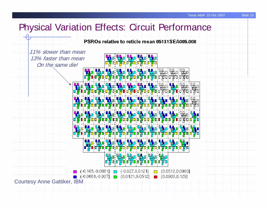
Courtesy Anne Gattiker, IBM
Physical Variation Effects: Circuit Performance
11% slower than mean13% faster than mean
On the same die!

Slide 14Texas A&M 23 Oct 2007
Variation Effects: Not just ring oscillators….Real Microprocessors
Multicore design -- Core-0 was found to be ~15% slower than other parts.Models predict all parts of the design are identical.
Core-0
Core-1
Cache

Slide 15Texas A&M 23 Oct 2007
Random Dopant Fluctuation
Threshold Voltage is dependant upon the doping within a device channel area.
The number of dopant atoms in the depletion layer of a MOSFET has been scaling roughly as Leff1.5.Statistical variation in the number of dopants, N, varies as N1/2, causing increasing Vt uncertainty for small N.
Source: D. Frank, et al, VLSI Tech 99, D. Frank, H. Wong IWCE, May 2000]
>200mV Vt Shift

Slide 16Texas A&M 23 Oct 2007
Random Dopant Fluctuation Effect
Performance, power, and leakage variation
Source: K. Agarwal, VLSI 2006
>200mV Vt Shift: ~100x leakage

Slide 17Texas A&M 23 Oct 2007
NBTI and Hot-carrier-induced VariationNegative Bias Temperature Instability
At high negative bias and elevated temperature the pFETVt gradually shifts more and more negative (reducing the pFET current).
The mechanism is thought to be the breaking of hydrogen-silicon bonds at the Si/SiO2 interface, creating surface traps and injecting positive hydrogen-related species into the oxide.Associated with the average NBTI shift, there are also random shifts, which even for identical use conditions and devices, will cause mismatch shifts due to random variations in the number and spatial distribution of the charges/interface states formed.
There are also other charge trapping and hot-carrier defect generation mechanisms that cause long-term Vt shifts in both nFETs and pFETs. Long-term Vt shifts are parameter variations that must be accounted for in the design of circuits.
N. Rohrer, ISSCC 2006

Slide 18Texas A&M 23 Oct 2007
Gate Oxide Thickness FluctuationGate oxide variation
Exponential effect on gate tunneling currentsAffects device threshold, butsignificantly less important Vt variation factor than random-dopant fluctuation
0 1 2 3 4 5 6 7
x 10-8
0
1000
2000
3000
4000
5000
6000
7000
800010s0 Pull Down historgram
Current [A]
Bin
Cou
nt
1.1nm oxide is ~6 atomic layers.across a 300mm wafer (>109 atomic layers)

Slide 19Texas A&M 23 Oct 2007
Back-end Variability -- CMPChemical/Mechanical polishing
Introduces large systematic intra-layer interconnect thicknessAdditional inter-layer interconnect thickness effects as well
Copper
Oxide
Dishing Erosion
CMP Variation
Topography variation translated into focus variation for lines which
results in width variation

Slide 20Texas A&M 23 Oct 2007
Measured Variation: interconnect performanceNormalized metal resistance data over 3 months
1.0
3.0
1.5
2.0
2.5
Wafer means change over timeSome real outliers Source: Chandu Visweswariah,
C2S2 Robust Circuits Wkshp, 7/28/06
Slide 21Texas A&M 23 Oct 2007
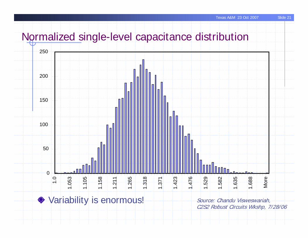
Normalized single-level capacitance distribution
0
50
100
150
200
2501.
0
1.05
3
1.10
5
1.15
8
1.21
1
1.26
5
1.31
8
1.37
1
1.42
3
1.47
6
1.52
9
1.58
2
1.63
5
1.68
8
Mor
e
Variability is enormous! Source: Chandu Visweswariah,C2S2 Robust Circuits Wkshp, 7/28/06

Slide 22Texas A&M 23 Oct 2007
Functional Variation
Workload variability – utilization of design based on changing workload requirements
time
Processorutilization
Source: J. Fredrich, ACEED ‘07~5% to ~95%

Slide 23Texas A&M 23 Oct 2007
Environmental Variation – Supply voltage
Supply variation due to input variation (eg. battery lifecycle) and self-generated and coupled supply noiseSupply variation affects performance, power, reliability
Power supply droop mapSource: Sani Nassif, IBM
VD
D
Chip Y (mm) Chi
p X
Source: P. Restle, ICCAD06, IBM
>10% dynamic supply droop

Slide 24Texas A&M 23 Oct 2007
Environmental Variation – Thermal
Thermal variation due to ambient fluctuation and self-heatingThermal variation affects performance, reliability
Die thermal map
Source: Sani Nassif, IBMSource: J. Friedrich, ACEED 2007
~30C dynamic temperature variation

Slide 25Texas A&M 23 Oct 2007
45nm technology and beyond
Is the VLSI Economy in jeopardy because of “variability?”
What is variability?What are the important sources of variability?What are the effects on VLSI design?How are fundamental design processes impacted?How can we cope?
Slide 26Texas A&M 23 Oct 2007
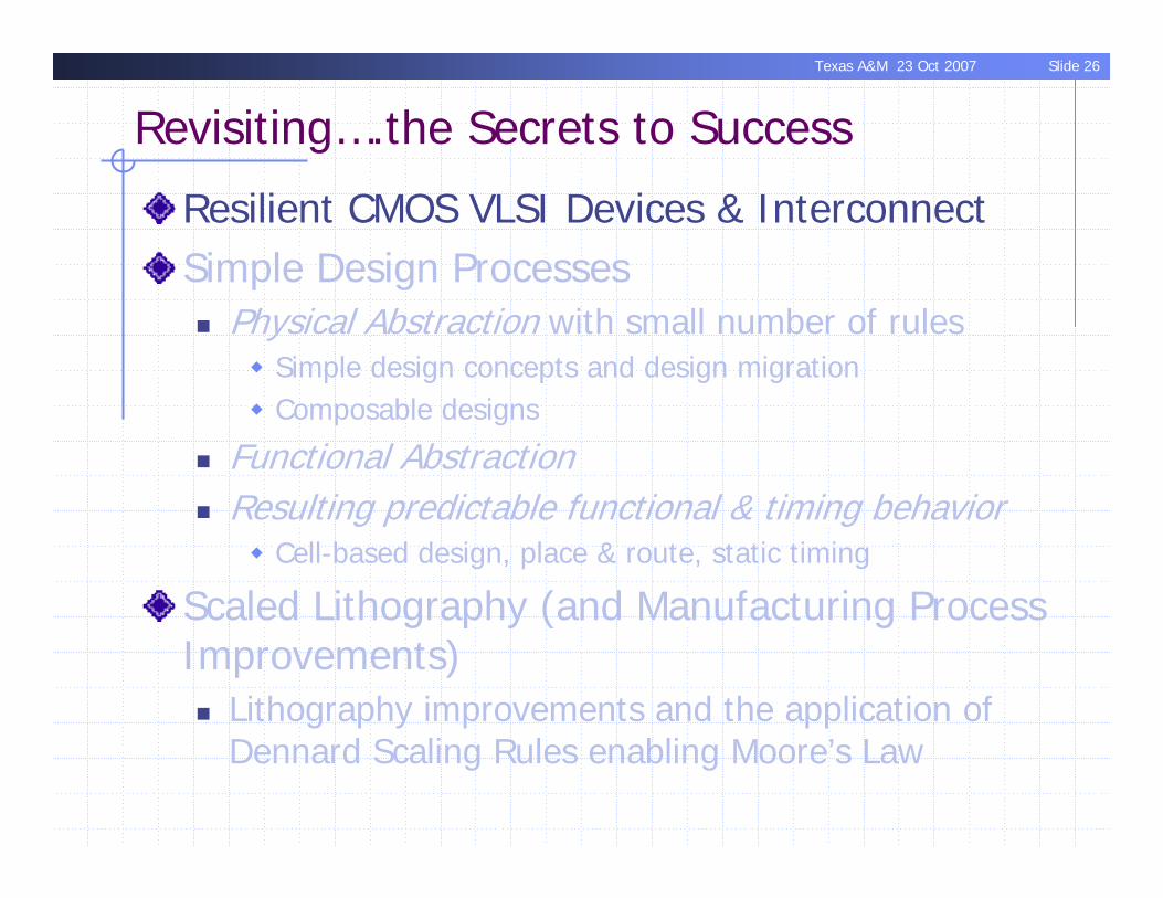
Revisiting….the Secrets to Success
Resilient CMOS VLSI Devices & InterconnectSimple Design Processes
Physical Abstraction with small number of rulesSimple design concepts and design migrationComposable designs
Functional AbstractionResulting predictable functional & timing behavior
Cell-based design, place & route, static timing
Scaled Lithography (and Manufacturing Process Improvements)
Lithography improvements and the application of Dennard Scaling Rules enabling Moore’s Law

Slide 27Texas A&M 23 Oct 2007
Technology Resiliency
Defects were the major yield detractors for technology in the early days, yield and area were the major tradeoffs.
λ = 365nm
λ = 248nm
λ = 193nm
0.01
0.1
1
'86 '88 '90 '92 '94 '96 '98 '00 '02 '04 '06 '08 '10
ISQED ’03, Dan Maynard, “Productivity Optimization Techniques for the Proactive Semiconductor Manufacturer”

Slide 28Texas A&M 23 Oct 2007
The Resiliency Problemλ = 365nm
λ = 248nm
λ = 193nm
0.01
0.1
1
'86 '88 '90 '92 '94 '96 '98 '00 '02 '04 '06 '08 '10
Contact ResistanceContact Resistance
1Ω 1MΩ
CircuitOK
CircuitNot OK
100Ω
Distribution of“Good” contacts
Distribution of“Bad” contact
Near futuredistribution
Fails that looklike opens!
Other factors, like the environment, make the failure region fuzzy and broad!
With scaling, variability – both random and systematic – has emerged as a source of performance and yield loss.
This can be viewed as the merger of failure modes due to structural (topological), and parametric (variability) defects.In the very near future, we will have to deal with circuits where a non-trivial portion of the devices simply do not work!

Slide 29Texas A&M 23 Oct 2007
What has changed?Resiliency & redundancy cannot be ignored.
Need to start design assuming partial functionality!
Mead-Conway design is dead…Physical abstraction is broken – ground-rule explosion Physical abstraction is broken – composability in
jeopardyFunctional abstraction is broken – increasingly difficult
to treat these as “logic devices”Transistor performance determined by new features
and phenomena, â large variety in behaviors (not easily bounded).
Key Factor: Variability
Slide 30Texas A&M 23 Oct 2007
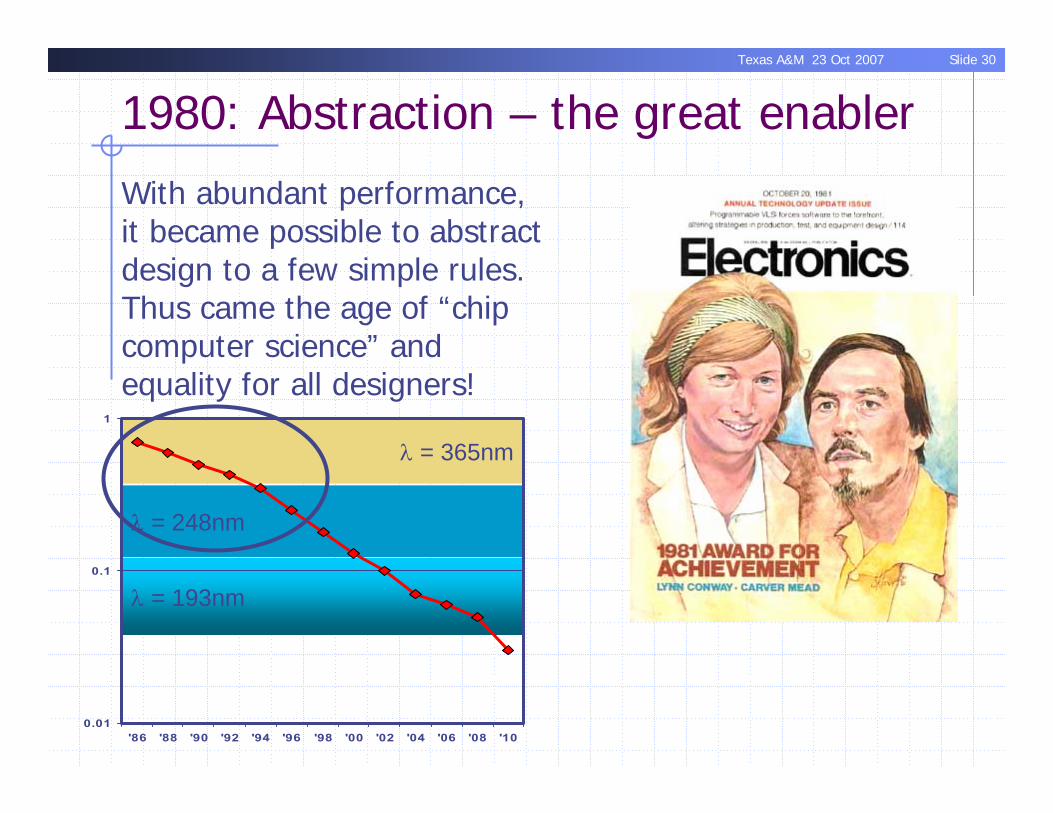
1980: Abstraction – the great enabler
With abundant performance, it became possible to abstract design to a few simple rules. Thus came the age of “chip computer science” and equality for all designers!
λ = 365nm
λ = 248nm
λ = 193nm
0.01
0.1
1
'86 '88 '90 '92 '94 '96 '98 '00 '02 '04 '06 '08 '10


