TECH. CORP.
SPECIFICATIONS
CUSTOMER : PTC
SAMPLE CODE : SH102600T003-IBA
MASS PRODUCTION CODE : PH102600T003-IBA
SAMPLE VERSION : 01
SPECIFICATIONS EDITION : 002
DRAWING NO. (Ver.) : LMD-PH102600T003-IBA (Ver.002)
PACKAGING NO. (Ver.) : PKG-PH102600T003-IBA (Ver.002)
Customer Approved
Date:
Approved Checked Designer
黃秋源
Oliver Huang
李健弘
Lambert Lee
黃俊清
Ackey Huang
□ Preliminary specification for design input
■ Specification for sample approval
POWERTIP TECH. CORP. Headquarters: No.8, 6th Road, Taichung Industrial Park,
Taichung, Taiwan
台中市 407工業區六路 8號
TEL: 886-4-2355-8168
FAX: 886-4-2355-8166
E-mail: [email protected]
Http://www.powertip.com.tw
NO.PT-A-005-8
PH102600T003-IBA Page2 SAMPLE Ver.01
SPEC Edi.002
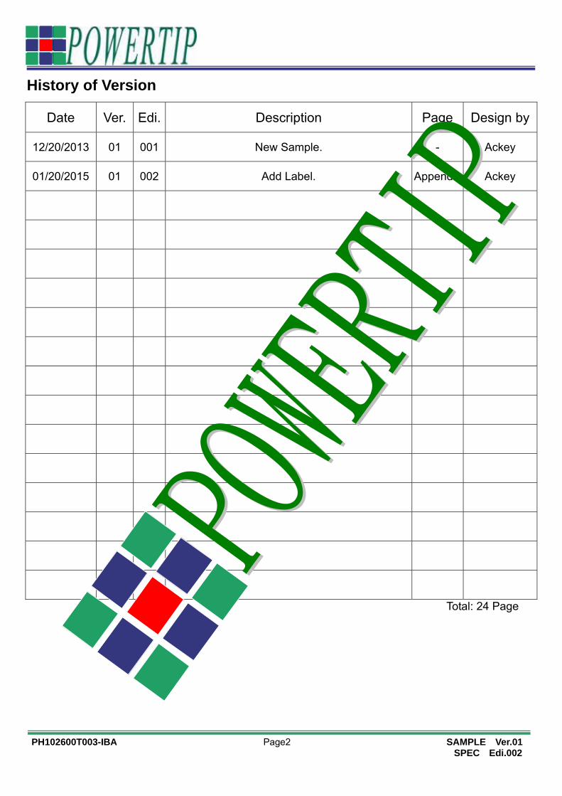
History of Version
Date Ver. Edi. Description Page Design by
12/20/2013 01 001 New Sample. - Ackey
01/20/2015 01 002 Add Label. Appendix Ackey
Total: 24 Page
PH102600T003-IBA Page3 SAMPLE Ver.01
SPEC Edi.002
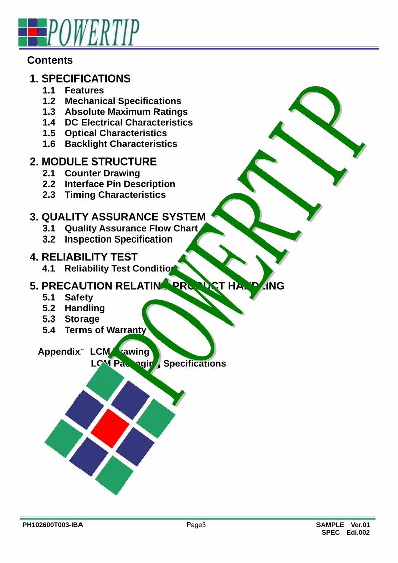
Contents
1. SPECIFICATIONS 1.1 Features 1.2 Mechanical Specifications 1.3 Absolute Maximum Ratings 1.4 DC Electrical Characteristics 1.5 Optical Characteristics 1.6 Backlight Characteristics
2. MODULE STRUCTURE 2.1 Counter Drawing 2.2 Interface Pin Description 2.3 Timing Characteristics 3. QUALITY ASSURANCE SYSTEM 3.1 Quality Assurance Flow Chart 3.2 Inspection Specification
4. RELIABILITY TEST 4.1 Reliability Test Condition
5. PRECAUTION RELATING PRODUCT HANDLING 5.1 Safety 5.2 Handling 5.3 Storage 5.4 Terms of Warranty
Appendix:LCM Drawing
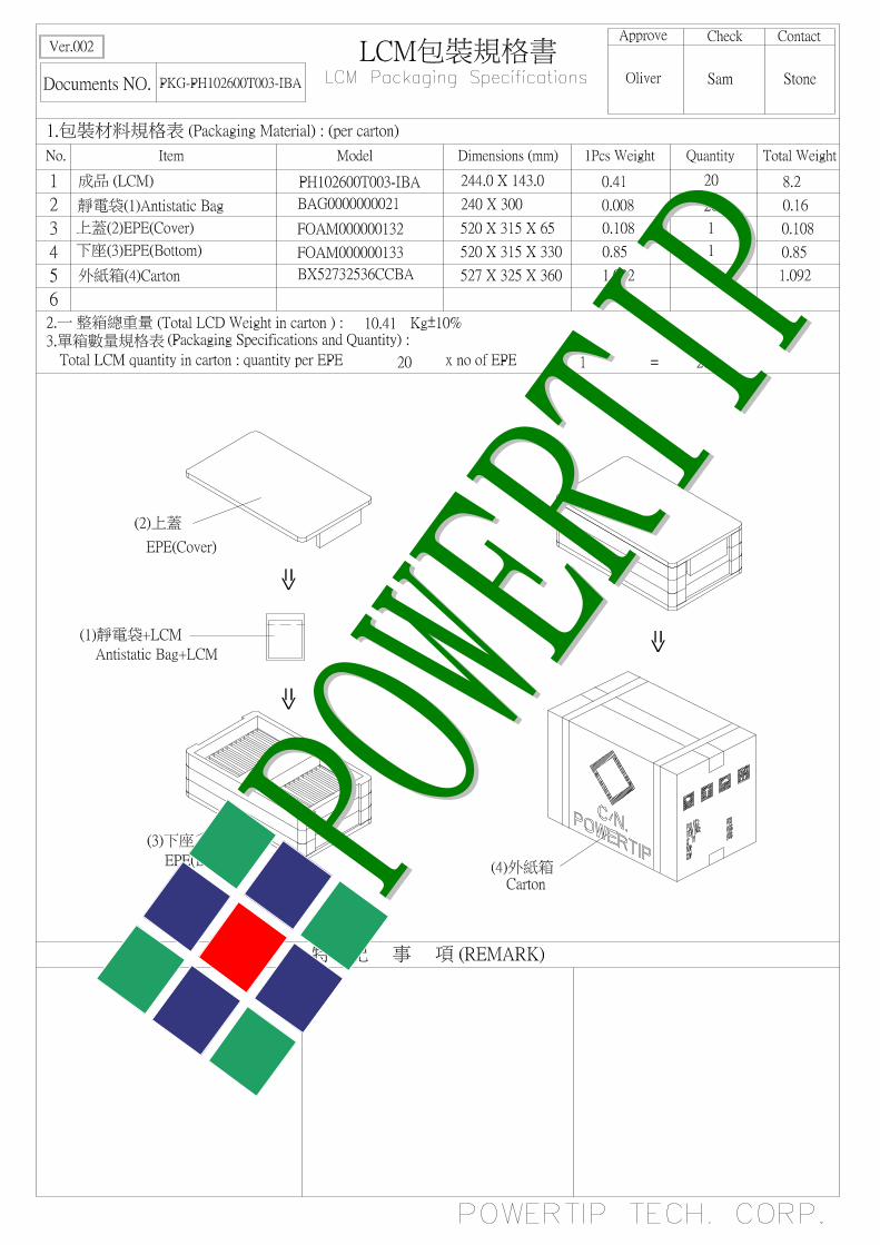
LCM Packaging Specifications

PH102600T003-IBA Page4 SAMPLE Ver.01
SPEC Edi.002
1. SPECIFICATIONS
1.1 Features Main LCD Panel
Item Standard Value
Display Type 1024* (R、G、B) * 600 Dots
LCD Type Normally white
Screen size(inch) 10.1(Diagonal)
Surface treatment Anti-glare, Hard-Coating(3H)
Color configuration R.G.B. vertical stripe
Backlight White LED
Interface LVDS
ROHS
THIS PRODUCT CONFORMS THE ROHS OF PTC
Detail information please refer website :
http://www.powertip.com.tw/news.php?area_id_view=1085560481/
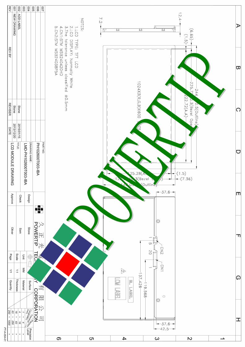
1.2 Mechanical Specifications
Item Standard Value Unit
Outline Dimension 244.0(W) * 143.0 (L) * 12.4 (H) mm
LCD panel
Item Standard Value Unit
Active Area 222.72 (W) * 125.28 (L) mm
Note : For detailed information please refer to LCM drawing
PH102600T003-IBA Page5 SAMPLE Ver.01
SPEC Edi.002
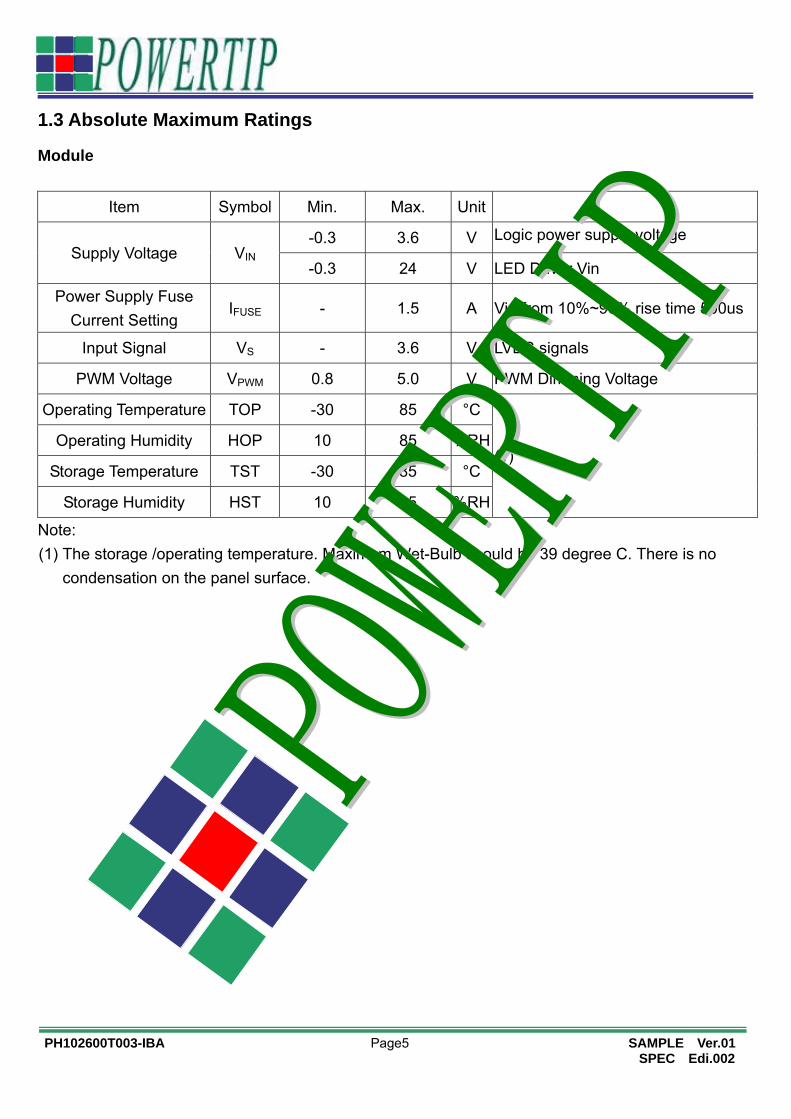
1.3 Absolute Maximum Ratings
Module
Item Symbol Min. Max. Unit
Supply Voltage VIN -0.3 3.6 V Logic power supply voltage
-0.3 24 V LED Driver Vin
Power Supply Fuse
Current Setting IFUSE - 1.5 A Vin from 10%~90%,rise time 500us
Input Signal VS - 3.6 V LVDS signals
PWM Voltage VPWM 0.8 5.0 V PWM Dimming Voltage
Operating Temperature TOP -30 85 °C
(1) Operating Humidity HOP 10 85 %RH
Storage Temperature TST -30 85 °C
Storage Humidity HST 10 85 %RH
Note:
(1) The storage /operating temperature. Maximum Wet-Bulb should be 39 degree C. There is no
condensation on the panel surface.

PH102600T003-IBA Page6 SAMPLE Ver.01
SPEC Edi.002
1.4 DC Electrical Characteristics
System Power Supply
ITEM SYMBOL MIN. TYP. MAX. UNIT CONDITIONS
Input Power Supply Voltage VIN 3.0 3.3 3.6 V
Input Power Supply Current IVIN - - 191 mA Black pattern 60Hz
Input Inrush Current IRUSH - - 1.5 A 0.5ms rise
time(10%~90%)
Input Power Voltage Ripple VRPL - - 200 mV VP-P
REV VH 2.0 3.3 5.0 V -
VL - - 0.8 V -
LED Power Supply
ITEM SYMBOL MIN. TYP. MAX. UNIT CONDITIONS
Input Power Supply Voltage VLED-IN 8 12 16 V
Input Power Supply Current IIN - - 546 mA
EN/PWM VH 2.0 3.3 5.0 V
VL - - 0.8 V
LVDS Signals
ITEM SYMBOL MIN. TYP. MAX. UNIT CONDITIONS
Differential Input High Threshold Vth - - +100 mV Vcm=+1.2v
Differential Input High Threshold Vtl -100 - - mV Vcm=+1.2v
Magnitude Differential Input
Voltage |Vid| 200 - 600 mV
Common Mode Voltage Vcm 1.0 1.2 1.4 V Vth - Vtl = 200mV
Common Mode Voltage Offset △Vcm -50 - +50 mV Vth - Vtl = 200mV

PH102600T003-IBA Page7 SAMPLE Ver.01
SPEC Edi.002
1.5 Optical Characteristics TFT LCD Panel VDD=3.3V, Ta=25°C
Item Symbol Condition Min. Typ. Max. Unit -
Response time Tr + TfTa = 25°C θX, θY = 0 - 16 20 ms Note2
Viewing angle
Top θY+
CR ≥ 10
70 80 -
Deg. Note4Bottom θY- 70 80 -
Left θX- 70 80 - Right θX+ 70 80 -
Contrast ratio CR
Ta = 25°C θX , θY = 0
400 500 - - Note3
Color of CIE Coordinate (With B/L )
White X 0.255 0.305 0.355
- Note1
Y 0.275 0.325 0.375
Red X 0.529 0.579 0.629 Y 0.294 0.344 0.394
Green X 0.276 0.326 0.376 Y 0.541 0.591 0.641
Blue X 0.109 0.159 0.209 Y 0.081 0.131 0.181
Average Brightness
Pattern=white display IV
-
400 500 - cd/m2 Note1
Uniformity △B 75 - - % Note1
Note1:
1:△B=B(min) / B(max) × 100%
2:Measurement Condition for Optical Characteristics:
a:Environment: 25℃±5℃ / 60±20%R.H,no wind,dark room below 10 Lux at typical lamp
current and typical operating frequency.
b:Measurement Distance: 500 ± 50 ㎜ ,(θ= 0°)
c:Equipment: TOPCON BM-7 fast,(field 1°),after 10 minutes operation.
d:The uncertainty of the C.I.E coordinate measurement ±0.01,Average Brightness ± 4%
1 2 3
6 5 4
7 8 9
VIEW AREA
LCM
θθ
Colorimeter=BM-7 fast
500㎜
PH102600T003-IBA Page8 SAMPLE Ver.01
SPEC Edi.002
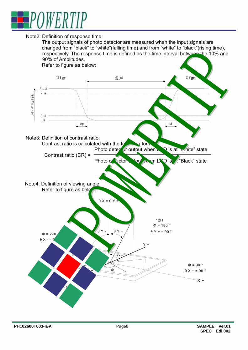
Note2: Definition of response time: The output signals of photo detector are measured when the input signals are changed from “black” to “white”(falling time) and from “white” to “black”(rising time),
respectively. The response time is defined as the time interval between the 10% and 90% of Amplitudes.
Refer to figure as below:
100%90%
10%0%
Signal (R
elative value)
"Black"
Tr Tf
"White" "White"
Note3: Definition of contrast ratio: Contrast ratio is calculated with the following formula Photo detector output when LCD is at “White” state Contrast ratio (CR) = Photo detector output when LCD is at “Black” state
Note4: Definition of viewing angle:
Refer to figure as below:
θ X - = 90 °
θ Y - = 90 °
X -
Y -
θ Y + = 90 °
θ X + = 90 °
X +
θ Y - θ Y +
θ X -θ X +
Y +
θ X = θ Y = 0°
Φ
Φ = 0 °6 H
Φ = 270 °
Φ = 90 °
Φ = 180 °12H
PH102600T003-IBA Page9 SAMPLE Ver.01
SPEC Edi.002
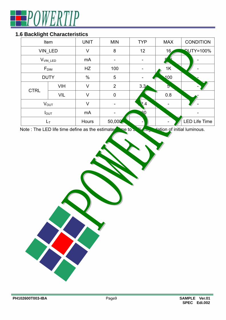
1.6 Backlight Characteristics
Item UNIT MIN TYP MAX CONDITION
VIN_LED V 8 12 16 DUTY=100%
VVIN_LED mA - - 543 -
FDIM HZ 100 - 1K -
DUTY % 5 - 100 -
CTRL VIH V 2 3.3 5 -
VIL V 0 - 0.8 -
VOUT V - 22.4 - -
IOUT mA - 160 - -
LT Hours 50,000 - - LED Life Time
Note : The LED life time define as the estimated time to 50% degradation of initial luminous.

PH102600T003-IBA Page10 SAMPLE Ver.01
SPEC Edi.002
2. MODULE STRUCTURE
2.1 Counter Drawing
2.1.1 LCM Mechanical Diagram
* See Appendix
2.1.2 Block Diagram
PH102600T003-IBA Page11 SAMPLE Ver.01
SPEC Edi.002
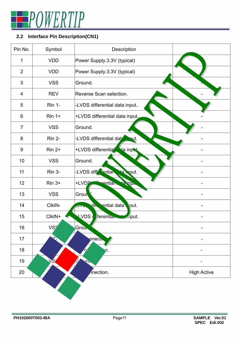
2.2 Interface Pin Description(CN1)
Pin No. Symbol Description
1 VDD Power Supply.3.3V (typical) -
2 VDD Power Supply.3.3V (typical) -
3 VSS Ground. -
4 REV Reverse Scan selection. -
5 Rin 1- -LVDS differential data input.. -
6 Rin 1+ +LVDS differential data input.. -
7 VSS Ground. -
8 Rin 2- -LVDS differential data input. -
9 Rin 2+ +LVDS differential data input. -
10 VSS Ground. -
11 Rin 3- -LVDS differential data input. -
12 Rin 3+ +LVDS differential data input. -
13 VSS Ground. -
14 ClkIN- -LVDS differential data input. -
15 ClkIN+ +LVDS differential data input. -
16 VSS Ground. -
17 NC Not connection. -
18 NC Not connection. -
19 VSS Ground. -
20 NC Not connection. High Active

PH102600T003-IBA Page12 SAMPLE Ver.01
SPEC Edi.002
B/L Pin Assignment(CN2)
Pin No. Symbol Description Remarks
1 VCC Power Supply. 12V(typical). -
2 GND Ground. -
3 EN 3.3V (typical) -
4 PWM 3.3V (typical) -
5 NC Not Connection -
PH102600T003-IBA Page13 SAMPLE Ver.01
SPEC Edi.002
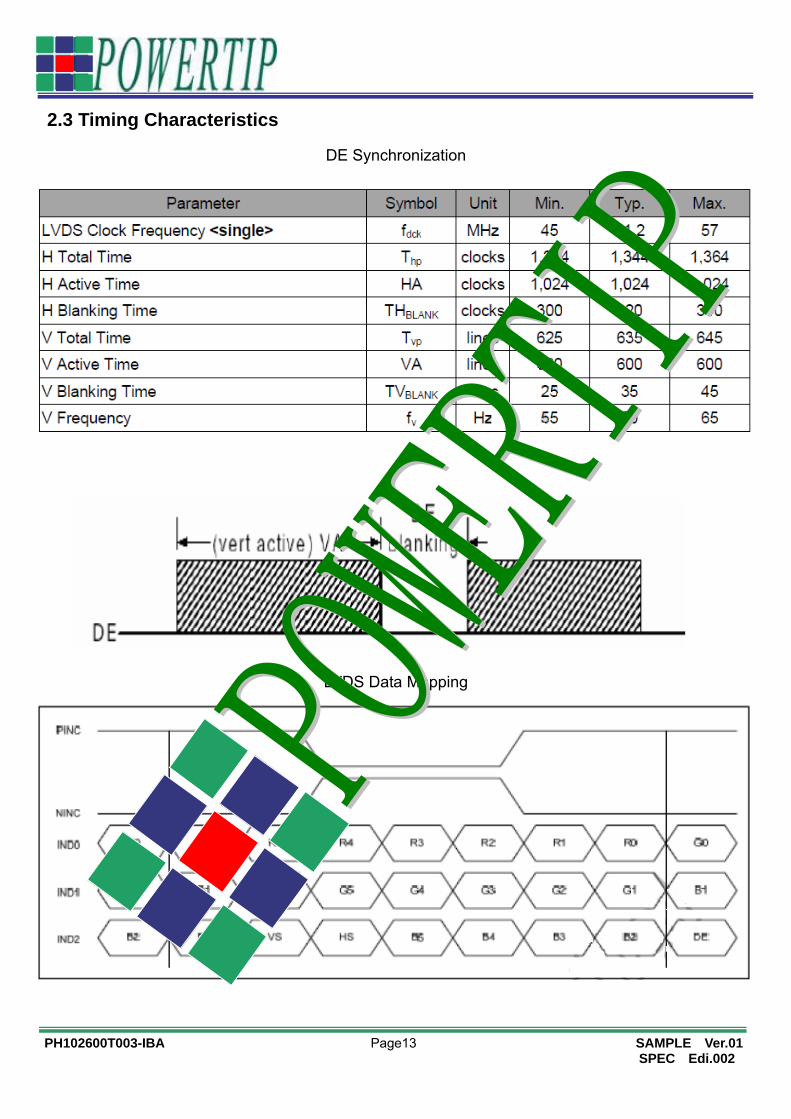
2.3 Timing Characteristics
DE Synchronization
LVDS Data Mapping

PH102600T003-IBA Page14 SAMPLE Ver.01
SPEC Edi.002
3. QUALITY ASSURANCE SYSTEM
3.1 Quality Assurance Flow Chart
Item Customer Sales R&D Q.A Manufactur
ing
Product
control Purchase
Inventory
control
Marketing
&
Design
Sample
Approval
Pilot
Run
&
Mass
Product
Ship
Out
OK
Request
Info Survey
Inquiry Project evaluation
Project Validation
Quote OK
NG
Contract
Design check
Sample test
Verification
Sample approval
NG
NG
Pilot run & Reliability test
Verification
Specification preparation OK
Mass production
Inspection NGOK
Shipment
NG
Ship out
OK

PH102600T003-IBA Page15 SAMPLE Ver.01
SPEC Edi.002
Item Customer Sales R&D Q.A Manufactu
ring
Product
control Purchase
Inventory
control
Sales
Service
Q.A
Activity
1. ISO 9001 Maintenance Activities 2. Process improvement proposal 3. Equipment calibration 4. Education And Training Activities 5. Standardization Management
Info Claim
Failure analysis
Corrective action
Tracking
Analysis report

PH102600T003-IBA Page16 SAMPLE Ver.01
SPEC Edi.002
3.2. Inspection Specification ◆Scope:The document shall be applied to TFT-LCD Module for 3.5〞~10.1〞(Ver.B01).
◆Inspection Standard:MIL-STD-105E Table Normal Inspection Single Sampling Level Ⅱ.
◆Equipment:Gauge、MIL-STD、Powertip Tester、Sample
◆Defect Level:Major Defect AQL: 0.4 ; Minor Defect AQL: 1.5
◆OUT Going Defect Level:Sampling.
◆Standard of the product appearance test:
a. Manner of appearance test:
(1). The test best be under 20W×2 fluorescent light,and distance of view must be at 30 cm.
(2). The test direction is base on about around 45˚ of vertical line.
(3). Definition of area.
(4). Standard of inspection: (Unit:mm)
A area : viewing area
B area : Outside of viewing area
PH102600T003-IBA Page17 SAMPLE Ver.01
SPEC Edi.002
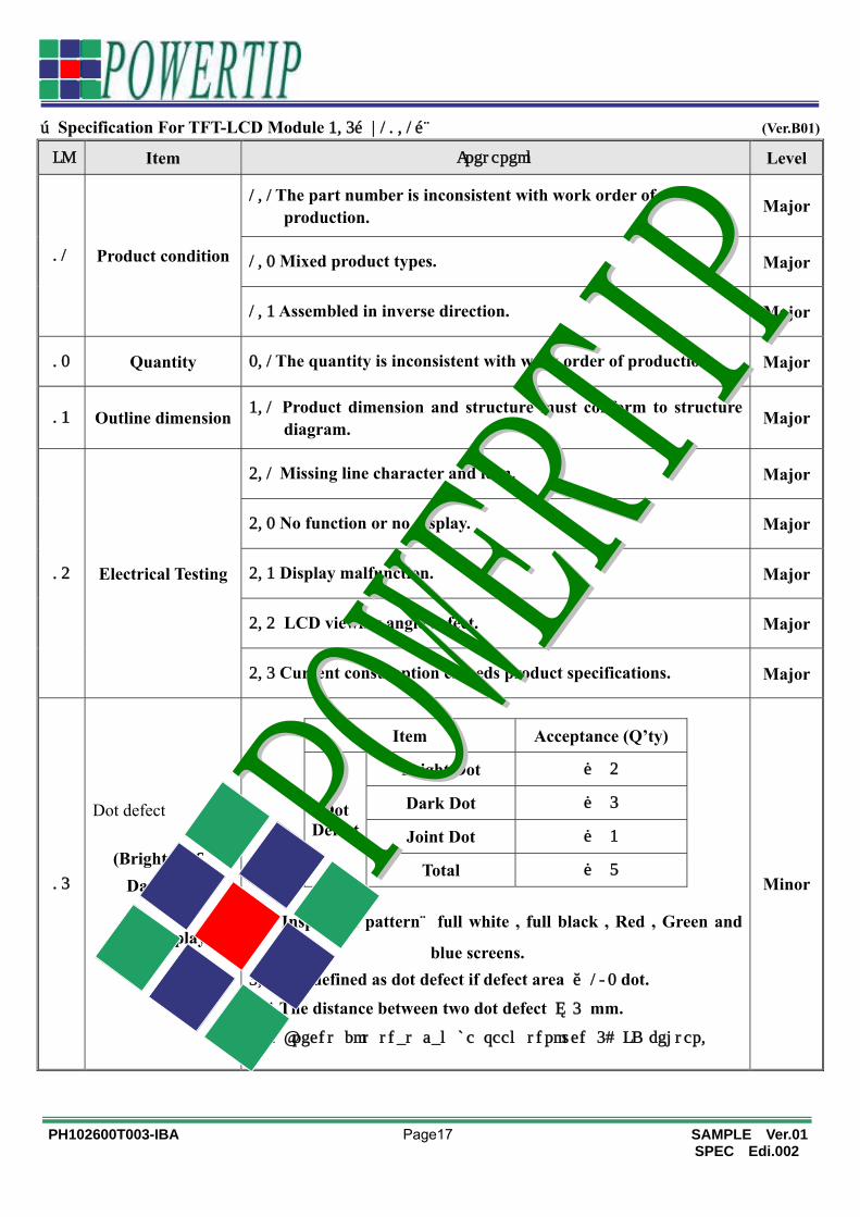
◆Specification For TFT-LCD Module 3.5〞~10.1〞: (Ver.B01)
NO Item Criterion Level
01 Product condition
1.1The part number is inconsistent with work order of production.
Major
1.2 Mixed product types. Major
1.3 Assembled in inverse direction. Major
02 Quantity 2.1The quantity is inconsistent with work order of production. Major
03 Outline dimension 3.1 Product dimension and structure must conform to structure
diagram. Major
04 Electrical Testing
4.1 Missing line character and icon. Major
4.2 No function or no display. Major
4.3 Display malfunction. Major
4.4 LCD viewing angle defect. Major
4.5 Current consumption exceeds product specifications. Major
05
Dot defect
(Bright dot、
Dark dot)
On -display
Item Acceptance (Q’ty)
Dot Defect
Bright Dot ≦ 4
Dark Dot ≦ 5
Joint Dot ≦ 3
Total ≦ 7
5.1 Inspection pattern:full white , full black , Red , Green and
blue screens.
5.2 It is defined as dot defect if defect area >1/2 dot.
5.3 The distance between two dot defect ≧5 mm.
5.4 Bright dot that can be seen through 5% ND filter.
Minor
PH102600T003-IBA Page18 SAMPLE Ver.01
SPEC Edi.002
◆Specification For TFT-LCD Module 3.5〞~10.1〞: (Ver.B01)
NO Item Criterion Level
06
Black or white dot、scratch、 contamination
Round type
6.1 Round type ( Non-display or display):
Dimension (diameter:Φ)Acceptance (Q’ty)
A area B area
Φ ≦ 0.25 Ignore
Ignore
0.25 < Φ ≦ 0.50 5
Φ > 0.50 0
Total 5
6.2 Line type( Non-display or display):
Length (L) Width (W) Acceptance (Q’ty)
A area B area
--- W ≦ 0.03 Ignore
Ignore
L ≦10.0 0.03 < W ≦ 0.05 4
L ≦5.0 0.05 < W ≦ 0.10 2
--- W >0.10 As round type
Total 5
Minor
07 Polarizer Bubble
Dimension (diameter:Φ) Acceptance (Q’ty) A area B area
Φ ≦ 0.25 Ignore
Ignore
0.25 < Φ ≦ 0.50 4
0.50 < Φ ≦ 0.80 1
Φ > 0.80 0
Total 5
Minor
X
Y
Φ=(x+y) / 2
W
L
Line type

PH102600T003-IBA Page19 SAMPLE Ver.01
SPEC Edi.002
◆Specification For TFT-LCD Module 3.5〞~10.1〞: (Ver.B01)
NO Item Criterion Level
08 The crack of glass
Symbols: X : The length of crack Y : The width of crack.Z : The thickness of crack W : terminal length t : The thickness of glass a : LCD side length
Minor
8.1 General glass chip:
8.1.1 Chip on panel surface and crack between panels:
X
Y
SP
【OK】
SP
【NG】
X Y Z
≦ a Crack can’t enter
viewing area ≦1/2 t
≦ a Crack can’t exceed the
half of SP width. 1/2 t < Z ≦2 t
X
YZ
YZ
XY
Z
Seal width

PH102600T003-IBA Page20 SAMPLE Ver.01
SPEC Edi.002
◆Specification For TFT-LCD Module 3.5〞~10.1〞: (Ver.B01)
NO Item Criterion Level
08 The crack of glass
Symbols: X : The length of crack Y : The width of crack. Z : The thickness of crack W : terminal length t : The thickness of glass a : LCD side length
Minor
8.1.2 Corner crack:
8.2 Protrusion over terminal:
8.2.1 Chip on electrode pad:
Z
X Y
X Y Z
Front ≦ a ≦ 1/2 W ≦ t
Back ≦ a ≦ W ≦ 1/2 t
X
Y
Z
X Y Z
≦1/5 a Crack can’t enter viewing area
Z ≦ 1/2 t
≦1/5 a Crack can’t exceed the half of SP width.
1/2 t < Z ≦ 2 t
W

PH102600T003-IBA Page21 SAMPLE Ver.01
SPEC Edi.002
◆Specification For TFT-LCD Module 3.5〞~10.1〞: (Ver.B01)
NO Item Criterion Level
08 The crack of
glass
Symbols: X : The length of crack Y : The width of crack. Z : The thickness of crack W : terminal length t : The thickness of glass a : LCD side length
Minor
8.2.2 Non-conductive portion:
☉ If the chipped area touches the ITO terminal, over 2/3 of
the ITO must remain and be inspected according to electrode
terminal specifications.
8.2.3 Glass remain :
X Y Z
≦ a ≦ 1/3 W ≦t
X Y Z
≦ 1/3 a ≦ W ≦t

PH102600T003-IBA Page22 SAMPLE Ver.01
SPEC Edi.002
◆Specification For TFT-LCD Module 3.5〞~10〞: (Ver.B01)
NO Item Criterion Level
09 Backlight elements
9.1 Backlight can’t work normally. Major
9.2 Backlight doesn’t light or color is wrong. Major
9.3 Illumination source flickers when lit. Major
10 General
appearance
10.1 Pin type、quantity、dimension must match type in structure
diagram. Major
10.2 No short circuits in components on PCB or FPC . Major
10.3 Parts on PCB or FPC must be the same as on the
production characteristic chart .There should be no wrong
parts , missing parts or excess parts.
Major
10.4 Product packaging must the same as specified on packaging
specification sheet. Minor
10.5 The folding and peeled off in polarizer are not acceptable. Minor
10.6 The PCB or FPC between B/L assembled distance(PCB or
FPC ) is ≦1.5 mm. Minor

PH102600T003-IBA Page23 SAMPLE Ver.01
SPEC Edi.002
4. RELIABILITY TEST
4.1 Reliability Test Condition
NO. TEST ITEM TEST CONDITION
1 High Temperature
Storage Test Keep in +80 ±2℃ 96 hrs Surrounding temperature, then storage at normal condition 4hrs.
2 Low Temperature
Storage Test Keep in -30 ±2℃ 96 hrs Surrounding temperature, then storage at normal condition 4hrs.
3 High Temperature /
High Humidity Storage Test
Keep in +60℃ / 90% R.H duration for 96 hrs Surrounding temperature, then storage at normal condition 4hrs. (Excluding the polarizer)
4 Temperature Cycling
Storage Test
-30℃ → +25℃ → +80℃ → +25℃
(30mins) (5mins) (30mins) (5mins)
10 Cycle
Surrounding temperature, then storage at normal condition 4hrs.
5 ESD Test
Air Discharge:
Apply 2 KV with 5 times Discharge for each polarity +/-
Contact Discharge:
Apply 250 V with 5 times discharge for each polarity +/-
1. Temperature ambiance : 15℃∼35℃ 2. Humidity relative : 30%∼60% 3. Energy Storage Capacitance(Cs+Cd) : 150pF±10% 4. Discharge Resistance(Rd) : 330Ω±10% 5. Discharge, mode of operation : Single Discharge (time between successive discharges at least 1 sec) (Tolerance if the output voltage indication : ±5%)
6
Vibration Test (Packaged)
1. Sine wave 10∼55 Hz frequency (1 min)
2. The amplitude of vibration :1.5 mm
3. Each direction (X、Y、Z) duration for 2 Hrs
7 Drop Test (Packaged)
Drop direction :※1 corner / 3 edges / 6 sides each 1times
Packing Weight (Kg)
Drop Height (cm)
0 ~ 45.4 122
45.4 ~ 90.8 76
90.8 ~ 454 61
Over 454 46
(Ver.B01)
PH102600T003-IBA Page24 SAMPLE Ver.01
SPEC Edi.002
5. PRECAUTION RELATING PRODUCT HANDLING 5.1 SAFETY
5.1.1 If the LCD panel breaks , be careful not to get the liquid crystal to touch your skin. 5.1.2 If the liquid crystal touches your skin or clothes , please wash it off immediately by
using soap and water.
5.2 HANDLING
5.2.1 Avoid any strong mechanical shock which can break the glass. 5.2.2 Avoid static electricity which can damage the CMOS LSI—When working with the
module , be sure to ground your body and any electrical equipment you may be using. 5.2.3 Do not remove the panel or frame from the module.
5.2.4 The polarizing plate of the display is very fragile. So , please handle it very carefully, do not touch , push or rub the exposed polarizing with anything harder than an HB pencil lead (glass , tweezers , etc.)
5.2.5 Do not wipe the polarizing plate with a dry cloth , as it may easily scratch the surface of plate.
5.2.6 Do not touch the display area with bare hands , this will stain the display area. 5.2.7 Do not use ketonics solvent & aromatic solvent. Use with a soft cloth soaked with a
cleaning naphtha solvent. 5.2.8 To control temperature and time of soldering is 320 ± 10°C and 3-5 sec. 5.2.9 To avoid liquid (include organic solvent) stained on LCM
5.3 STORAGE 5.3.1 Store the panel or module in a dark place where the temperature is 25°C ± 5°C
and the humidity is below 65% RH. 5.3.2 Do not place the module near organics solvents or corrosive gases.
5.3.3 Do not crush , shake , or jolt the module.
5.4 TERMS OF WARRANTY 5.4.1 Applicable warrant period
The period is within thirteen months since the date of shipping out under normal using and storage conditions.
5.4.2 Unaccepted responsibility This product has been manufactured to your company’s specification as a part for use in your company’s general electronic products. It is guaranteed to perform according to delivery specifications. For any other use apart from general electronic equipment, we cannot take responsibility if the product is used in nuclear power control equipment, aerospace equipment , fire and security systems or any other applications in which there is a direct risk to human life and where extremely high levels of reliability are required.