
S I G N A L A N D N O I S E C H A R A C T E R I S T I C S
O F P H O T O V O L T A I C P - N J U N C T I O N D I O D E S
by
DONALD STEWART GALBRAITH
B. A. , University of British Columbia, 1955
A THESIS SUBMITTED IN PARTIAL F U L F I L M E N T OF
T H E REQUIREMENTS FOR T H E DEGREE OF
MASTER OF SCIENCE
in the Department
of
Physics
We accept this thesis as conforming to the
required standard
THE UNIVERSITY OF BRITISH COLUMBIA
December, 1957

i i
A B S T R A C T
The noise c h a r a c t e r i s t i c s of ideal photovoltaic p-n junction
diodes are discussed and investigated. The hypothesis i s advanced that
the open-circuit noise from an illuminated ideal diode is e n t i r e l y due
to the shot noise of the various current contributions. T h e o r e t i c a l
ju s t i f i c a t i o n for this theory is developed and the parameter t, the
effective noise temperature r a t i o , i s introduced. The possible reasons
for excess noise i n p-n photo-diodes observed i n e a r l i e r experiments
are suggested.
The dc and ac behavior of a r e a l diode chosen to be very
nearly ideal i n its dc c h a r a c t e r i s t i c i s found to be consistent with
existing diode theory. The various parameters appropriate to the device
are evaluated.
Equipment for noise measurement is selected and a
comparison technique adopted. This method avoids many of the possible
e r r o r s inherent in an absolute measurement and allows an equivalent
noise resistance resolution of about 200 ohms at room temperature i n
the 200 cs bandwidth measured. The open-circuit noise of the selected
diode is measured at 20 and 30 kc as a function of il l u m i n a t i o n and the
results interpreted i n terms of the equivalent resistance in thermal
equilibrium which would give the same noise. Comparison of this set
of values with the r e a l part of the junction impedance in each case
indicates thatthe £heory advanced is adequate to predict noise under
these circumstances.
The signal-to-noise r a t i o for a photo-diode used as an
open-circuit radiation detector is developed, and se v e r a l recommendations

i i i
are made regarding the design of a photo-diode to display the most
favourable signal-to-noise ratio under illumination.

In presenting t h i s thesis i n p a r t i a l fulfilment of
the requirements fo r an advanced degree at the University
of B r i t i s h Columbia, I agree that the Library s h a l l make
i t f r e e l y available for reference and study. I further
agree that:permission for extensive copying of t h i s thesis
for scholarly purposes may be granted by the Head of my
Department or by his representative. It i s understood
that copying or publication of t h i s thesis f o r f i n a n c i a l
gain s h a l l not be allowed without my written permission.
Department of P W J ^
The University of B r i t i s h Columbia, Vancouver 8, Canada.

iv
T A B L E O F C O N T E N T S
Chapter Page
1 INTRODUCTION 1
1. 1 Review of Previous Work 1
1. 2 Theoretical Considerations 6
1. 3 Objective of Present Work 12
2 E X P E R I M E N T A L INVESTIGATIONS 13
2. 1 Direct Current Characteristics 13
2.2 Alternating Current Measurements , 17
2. 3 Noise Measurements 24
3 . DISCUSSION OF RESULTS 30
3. 1 Inferences from DC and AC Measurements 30
3. 2 Implications of Noise Measurements 34
4 CONCLUSIONS 36
4. 1 General Comments 36
4. 2 Design Recommendations for Radiation Detectors 38
APPENDDC
Shift in DC Bias Due to Rectification of AC Signal from Measuring Bridge 42
BIBLIOGRAPHY 44

A C K N O W L E D G M E N T S
I wish to thank P r o f e s s o r R. E. Burgess for his guidance
throughout the course of this investigation and for his many valuable
comments during the preparation of this thesis.
The work described was c a r r i e d out under Defence
Research Board grant number" 9512-22. I also wish to thank the Board
for personal f i n a n c i a l assistance from A p r i l to December of 1957.
I am indebted to Mr. D. A. McCoy for his assistance
in the preparation of the figures.
D. S. G.
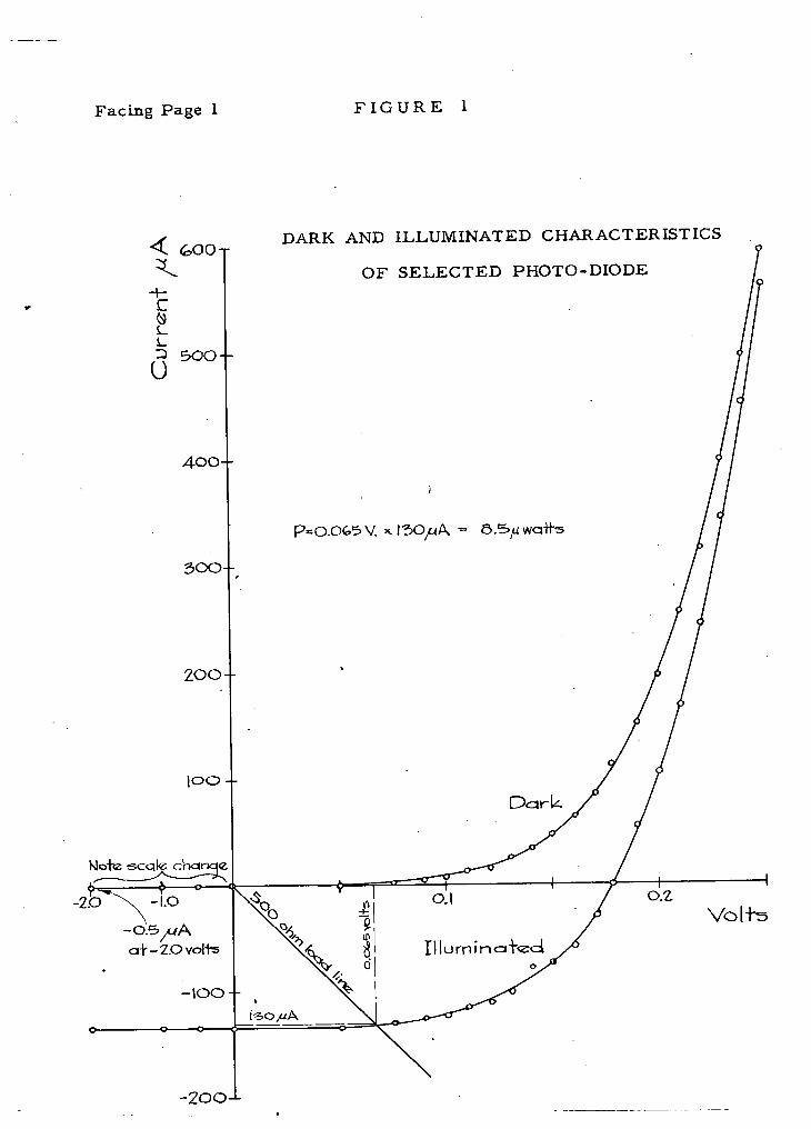
Facing Page 1 F I G U R E 1
- 2 0 0 - L

C H A P T E R 1 I N T R O D U C T I O N
1
1. 1 Review of Previous Work
Brief ly , a photovoltaic p-n junction diode is a solid state
device capable of converting incident illumination (of suitable wavelength)
into electr ical energy. Its operation as a circuit element can best be
outlined by reference to figure 1. The dark characteristic plotted here
is s imi lar to that of an ideal diode. Shockley (1949) has derived the
following relation between current (I) and voltage (V) for an ideal p-n
junction diode;
I = I o ( e x p - g - 1), (1)
where Io = reverse saturation current q = electronic charge k = Boltzmann's constant T = absolute temperature of junction.
To do so he assumed that the transition region between n and p regions
has negligible width compared to the diffusion lengths of the ca r r i e r s ,
and that the currents involved are smal l (such that the injected carr ier
density in either region is smal l compared to the density of the carr ier
normally present therein).
Later Cummerow (1954) considered the case occurring
when photons of energy greater than the energy gap of the semiconductor
fall on or near the junction creating hole-electron pairs which, crossing
the junction unsymmetrical ly because of the electrostatic field existing
there, constitute an additional current. He showed that the current
flow in this case is given by
I = U e x p ^ - 1) - B L (2)
where B L , the photocurrent, is proportional to the incident light

2
intensity L.' In other words, the illumination causes a proportional
current contribution in the opposite direction to the forward dark
current. In effect, then, illumination drops the diode's dark
ch a r a c t e r i s t i c by an amount BL, as is indicated by the curve in figure 1
for an illuminated device.
That portion of the curve fa l l i n g i n the fourth quadrant is
of p a r t i c u l a r interest because it is the portion generated by the
illuminated device and a passive load alone. The point of intersection
of the appropriate illuminated c h a r a c t e r i s t i c with a load line drawn
from the o r i g i n indicates the voltage across and current through that
load under that illumination and thus shows the power delivered to the
load. F o r example, the diode tested would deliver about 8. 5 microwatts
(130//A at 65 mv) to a 500 ohm load at the i l l u m i n a t i o n l e v e l plotted.
It should be noted that r e a l devices (including that for which
figure 1 was plotted) exhibit various departures from ideal behavior.
Several of these departures w i l l be considered in later sections.
Although these diodes are finding numerous applications
as radiation detectors or energy convertors, r e l a t i v e l y l i t t l e attention
has been paid to certain aspects of their properties. In p a r t i c u l a r , no
thorough investigation of their noise behavior under illumination has
been performed.
Several sets of measurements have been made, however.
Gianola (1956) investigated s i l i c o n broad area junctions under open-
c i r c u i t conditions at various incident light intensities and in the frequency
range from 20 cs to 4 kc. His results indicate a l/frequency noise
voltage squared spectrum under constant illumination and a varying

3
noise magnitude with varying illumination. This v a r i a t i o n of noise
voltage is quite marked and passes through a maximum which appears
reasonably independent of frequency over the range investigated. He
explained his results on the basis of current-dependent fluctuations
of current.
Sp e c i f i c a l l y , he assumes that the mean square current
fluctuation is d i r e c t l y proportional to the photocurrent ( B L in equation 2)
and thus to the illumination; i . e. ,
~i*= s q B L A f
where s is independent of the magnitude of the photocurrent but is a
function of frequency. The measured mean square voltage fluctuation,
however, is the product of this current fluctuation with the square of
the dynamic impedance of the junction. This latter term decreases
with increasing illumination (under open-circuit conditions) so the
maximum in the noise voltage versus illumination plot is quantitatively
reasonable,
Gianola's assumption for the form of the current noise is
rather suggestive of the shot noise equation
"F=2qlAf.
Any attempt to apply this equation d i r e c t l y to a p-n junction, however,
is complicated by the necessity of sorting out the contributions of the
various c a r r i e r s to the current and, assuming their individual motions
to be essenti a l l y uncorrelated, adding up their contributions to the
noise. Gianola's diode exhibited current noise of the order of 10 4
greater than that which would result from shot noise in a vacuum diode
c a r r y i n g a current equal to the p-n diode's photocurrent.

4
The objection might be r a i s e d that the broad area junctions
used in this investigation are notoriously poor diodes, especially in
that their reverse dc c h a r a c t e r i s t i c s indicate a rather low shunt
resistance. This being the case, the preceding study was not actually
made under open-circuit conditions, since r e l a t i v e l y heavy currents
could flow internally. s
To incorporate the non-ideal behavior of the device studied,
Gianola fitted its c h a r a c t e r i s t i c s to those predicted by the Bethe model
(Torrey and Whitmer, 1948). The equation for the dc c h a r a c t e r i s t i c s
of this model diff e r s from that of Shockley's (equation 1) by replacing
the latter's I 0 w i t h a term Ioexp(-yS-£^), where 0^8^1/2. Although there is
a theoretical basis for its application to point-contact diodes, the equation
can be,applied to junction diodes only on e m p i r i c a l grounds. The
effect of the extra factor is to lower the c h a r a c t e r i s t i c from the ideal
(Shockley) curve for both forward and reverse bias, v i z ;
Poor reverse diode behavior, however, can generally be explained
in terms of low shunt resistance, while reduced forward current indicates
series resistance or high c a r r i e r injection (violating Shockley's
assumption). Since the forward and reverse non-ideal c h a r a c t e r i s t i c s
stem from different causes, it is unreasonable to expect an additional
term involving only one extra parameter to provide more than a rough,

e m p i r i c a l correction.
Another study by Pearson, Montgomery, and Feldmann
(1955) points up one of the dangers encountered i n this f i e l d . T heir
measurements indicate that a nearly ideal s i l i c o n p-n diode illuminated
and reverse biased to give a current of the order of 10 4 times I 0 e x h i b i t s
p r e c i s e l y shot noise down to f a i r l y low frequencies (80 cs). When the
reverse saturation current is r a i s e d by a factor of about 100 by exposing
the device to very humid a i r , the noise behavior changes markedly;
exhibiting a l/frequency current-squared spectrum with a 100 cs value
about 10 e above shot noise. These results indicate (as indeed the authors
concluded) that excess noise i n semiconductor devices can be a strongly
surface-dependent property.
Noise measurements have been made on an InSb
photovoltaic c e l l ( M i t c h e l l , Goldberg, and Kurnich, 1955) under
illumination. A l/frequency 3noise voltage-squared spectrum is reported
below 2 kc with substantially white noise (mean squared noise voltage
constant with frequency) from 2 kc up to about 200 kc. Once again,
however, the task of a s c r i b i n g the noise generation to a simple
mechanism is complicated by the non-ideal nature of the device which,
according to the authors, 'exhibited . . . no noticeable r e c t i f i c a t i o n . *

6
1. 2 Theoretical Considerations
At present, there is no all-embracing theory for the noise
behavior of an ideal p-n photo-diode although s e v e r a l reasonable
conjectures may be made. Obviously, Nyquist's theorem must apply to
an open-circuited diode in the dark when in thermal equilibrium whether
the noise is considered from the thermodynamic or the corpuscular
point of view.
To il l u s t r a t e t h i s , consider an ideal Shockley diode in
thermal equilibrium. Its c h a r a c t e r i s t i c s are then given by equation 1
which may be interpreted as predicting a current L>expS^ i n the forward
dire c t i o n and I 0 in the reverse direction. If we assume these currents
to be m i c r o s c o p i c a l l y uncorrelated (or more exactly, if we assume the
c a r r i e r t r a n s i t s comprising these currents occur independently and
randomly at mean r a t e s - ^ e x p ^ ^ and-^respectively) we may write the
shot noise equation as
2ql = 2ql 0(exp - g ^ + 1).
Since we have postulated thermal equ i l i b r i u m , V must be zero, so
4 q l 0 .
Differentiating equation 1 with respect to V and setting V equal to zero
gives for the low frequency open-circuit conductance
G = - § V = - § Y " » or q l 0 = kTG.
With this substitution, the shot noise equation becomes l* 4kTG
A f
which is Nyquist's thermodynamic result. Thus the thermodynamic and
corpuscular approaches have been shown to b(e compatible in thermal
equilibrium under the assumptions used.

Facing Page 7 F I G U R E 2 i
E L E C T R O S T A T I C P O T E N T I A L A N D Q U A S I - F E R M I L E V E L S
IN A N I L L U M I N A T E D P + - N J U N C T I O N
n
V v i

7
Under illumination, however, the situation could be more
complicated. Let us f i r s t describe in general terms the usual photo-diode
model. Figure 2 shows the internal distribution of the electrostatic
one-dimensional model. Here V and I, the voltage across and current
through the diode, are the same as those appearing in equation 2. - F o r
s i m p l i c i t y , the diode shown is p +-n, rather than p-n, because under this
condition v i r t u a l l y a l l the current in the n region at the junction is due
to hole diffusion.
F o r s m a l l injected c a r r i e r densities, the reverse current
ari s e s from holes diffusing from the n to the p + region at a rate
independent of the voltage across the junction but proportional to the
number of holes available for such diffusion. Thus the reverse current
is I Q+ BL, where I c, the macroscopic dark saturated reverse current,
corresponds to the thermally generated holes and i s proportional to the
equilibrium density of holes in the n region p n; being equal in fact
(Shockley, 1949), to Aqpn-f^-, where A is the area of the junction and Lip
Dp and L|6 are the diffusion constant and diffusion length respectively
for holes in the n region. The B L term accounts for the extra light-
created holes available for diffusion.
holes in the p + region having enough energy to surmount the junction
" potential b a r r i e r . This b a r r i e r i s lowered from its e quilibrium height
be a function of V and i s , in fact, I 0exp-^> It should be noted that the preceding discussion - subject
potential ijj and the q u a s i - F e r m i levels <ppand <p n(Shockley, 1949) for a
The forward current, on the other hand, a r i s e s from those

I
8
to the r e s t r i c t i v e assumption of low injected c a r r i e r density - is quite
independent of the cause of the voltage across the diode; this voltage
may be applied by an external battery, may be the open-circuit
photovoltage of the diode, or may be the photovoltage appearing across
an a r b i t r a r y load.
If we assume, as in the equilibrium case, that the
contributions to the total current are individually uncorrelated, we
may write the shot noise equation for the illuminated case as
= 2 q ( I 0 e x p ^ + I.+ BL).
We sh a l l now introduce a new variable t, the effective noise temperature
ra t i o , which we define as the ratio of the mean squared current or
voltage noise in a part i c u l a r case to that given by Nyquist's theorem
applied to the conductance or resistance. Thus for current noise
4kTG * Differentiating equation 2 with respect to V gives for the low frequency
diode conductance under illumination » G =4v="k%exPklT" = k T < 1 + *• + B L ) ' < 3 )
and hence t [ l + (1 + ^ " ) e x p ( - ^ ) ] . (4) To investigate the open-circuit case, I = 0 is substituted into equation 2 to give
e x p k T yi + u
- so that t [ l + exp V>].
The open-circuit noise temperature r a t i o , then, is
t-c=i(i + i ) = l
that i s , the open-rcircuit noise of an illuminated ideal diode i s , under

9
these assumptions, that expected from the same impedance in thermal
equilibrium. If current flows, however, increased noise may be expected
since then V < V o c f o r a given B L
Subject to our assumptions, then,we have shown that although
an open-circuited illuminated ideal diode exhibits thermal noise only,
use of the diode to deliver current to a load (or to accept current from
a source) w i l l increase the noise. The effect of current flow within the
device w i l l next be considered. This situation could a r i s e in an ideal
diode if the illumination were not perfectly uniform. Let us suppose,
for example and as a rough approximation, that hole-electron p a i r s are
being created by light uniformly in part of the diode (to which we may
thus apply equation 2), but are being produced only t h e r m a l l y i n the rest
of it (to which we may apply equation 1). Then we may represent the
system by two diodes i n p a r a l l e l :
Diode 1: I,= I o , ( e x p ^ _ 1 ) " B L
Diode 2: Iz= I 0 2 ( e x p - j ^ - 1)
where diodes 1 and 2 represent the illuminated and dark portions
respectively of the complete device. We s h a l l also assume the two
parts of the diode to be at the same temperature.
Proceeding in the same way as before, we write for the
shot noise density
- £ = 2q(Lwexp^-+ I0,+ B L ) kT

10
iif qV and ~M~= 2q ( I Q2exp k T + I0z) .
Hence = 2q[(I„,+ L ^ e x p - ^ + I0, + I0z+ B L J
The total current through the composite diode is
I = (Io,+ M e x p ^ - Uz) - B L
so that its low frequency conductance is _ dl_ _q_ . _q_V
G ~ dV ~ k T ^ I o l + *«/ e xPkT '
Then t = 4kTG
=*[1+<1+T3T;»^-S-'/-Since I c = I01+ Ioz. the noise temperature ratio is unchanged by the non-
uniformity of the illumination. In p a r t i c u l a r , i n the open-circuit condition qVoc , , B L
so that toc= 1. Thus the internal current produced in the diode by non-uniform
illumination does not cause an addition to the measurable noise. This
result s i m p l i f i e s the experimental techniques, since no sp e c i a l attention
need be paid to the homogeneity of the incident light beam or to the
detailed geometry of the junction.
The objection might reasonably be r a i s e d that the hole-
e l e c t r o n pairs produced by the light are being created with energies i n
many cages considerably in excess of the thermal energy of the c r y s t a l
l a t t i c e , and it would seem possible that p r i o r to thermalization these
pairs could lead to additional noise. Davydov (Tauc, 1957) has shown,
however, that this therm ali z a t i o n takes place in a time very short
compared with the life t i m e s of the m i n o r i t y c a r r i e r s : representative
figures being 10""seconds for the therm ali z a t i o n process and lO'^seconds

for a t y p i c a l lifetime. This is further support for the theory that the
noise under illumination should be predicted - at least approximately
by Nyquist's expressions, since the photocarriers w i l l have energies
corresponding to the lattice temperature except for a very short
i n i t i a l period of elevated energy.

12
1. 3 Objective of Present Work.
The objective of the present work is to provide an
experimental basis for a noise generation model which, it i s hoped,
w i l l predict the open-circuit noise voltage appearing at the terminals
of an illuminated photo-diode in terms of the measurable parameters
of that diode. In p a r t i c u l a r , it is proposed to investigate the
p o s s i b i l i t y of predicting this noise voltage on a 'quasi-Nyquist' basis;
that i s , can the noise of an illuminated device s t i l l be ascribed to the
Nyquist-predicted thermal noise of the r e a l part of the junction impedance
at the same frequency (as the noise measurement is made) and under
the same illumination?
To this end, a photo-diode has been selected whose direct
current c h a r a c t e r i s t i c s appear nearly ideal. Various measurements
are described from which the parameters characterizing the device can
be inferred. These include direct current measurements of s h o r t - c i r c u i t
current and open-circuit voltage under varying illumination, current
and voltage under constant illumination, and impedance at frequencies
from 1 to 100 kc under varying illumination. The diode's noise has
been measured (limited to frequencies from 20 to 30 kc by equipment
and techniques available) as a function of illumination and i n terms of
equivalent noise resistance.

13
C H A P T E R 2 - E X P E R I M E N T A L I N V E S T I G A T I O N S
2. 1 D i r e c t Current C h a r a c t e r i s t i c s
v
Photo-diodes available for selection were types 5C and
1N188A grown germanium p-n junctions manufactured by Clevite
T r a n s i s t o r Products. The direct current c h a r a c t e r i s t i c s of two of the
former and five of the latter were measured both in the dark and under
constant illumination, and one of the former was selected for further
investigation because of its near-ideal performance. The experimental
setup was as follows?
2 k n A/VWWV-
V a c u o m -voI+m<z
AA/ V ^ / T 1
The results of these measurements with the selected diode are those
shown in figure 1. The saturation evidenced by the reverse
c h a r a c t e r i s t i c indicates consistency with equations 1 and 2 for the dark
and light c h a r a c t e r i s t i c s respectively.
Further evidence for the app l i c a b i l i t y of these equations
is obtained by considering the photocharacteristic equation. Examining
equation 2 under s h o r t - c i r c u i t conditions (V = 0) gives
Isc= -BL (5) and under open-circuit conditions (I = 0) gives
0 = I 0 ( e x p ^ f - 1) - B L .

Facing Page 14 F I G U R E 3
5 --
4 --
3 --
2 - -
-I --
FORWARD DARK, FORWARD ILLUMINATED,
AND PHOTOCHARACTERISTICS
OF S E L E C T E D DIODE
A Forward licjhf charachzr is l ic a Forward dark charctc+<zrbiic
°. P h o 4 " o c r i a r a c f < 2 r i s + i c
A a a
-"Slope = 2>75 v o l + 5 - 1
(-ft- = 39. G voi-hr' a l 20 ° C )
0 . 2
V o l t s
- — 1 ~ O . O Z Q j u A

14
Combining these gives the photocharacteristic equation for the model:
11̂ 1= I„(exp-g^- 1) (6)
or ln( | lsc| + I Q) = j ^ V ^ + ln(U) .
This equation i s of the same form as the forward dark char a c t e r i s t i c .
Thus a plot of ln ( | l sc |+ Io) versus Voo should be a straight line of slope
•r^L-if this model is valid. Figure 3 is such a plot and suggests rather
good agreement. It should be noted that the ordinate axis intercept of
the line obtained from the high current readings (such that |l s c|»I 0) gives
an approximation to ln(I„); using this value for I Q enables the plot of
ln ( | l sc |+ Io) to be completed at low currents. ,
The measurements for the photocharacteristic plot were
obtained using a heavily shunted m i r r o r - t y p e galvanometer for I s c , a
potentiometer for Voc, and a 150 watt incandescent projection lamp for
a light source. Variation of light intensity was provided for by running
the lamp from 60 cs power obtained through a variable autotransformer.
The optical arrangement consisted of a single converging lens of about
20 cm focal length to concentrate the light somewhat and a block of
clear lucite about 1 inch thick to minimize heating effects. The lucite
is a good absorber of those wavelengths greater than that corresponding
to the energy gap in germanium which would produce only heat i n the diode.
The slope of the photocharacteristic line i n figure 3 is
about 37. 5 volt"', whereas -j^-for room temperature (20°C) is 39. 6 volt" 1;
so the results are i n reasonable agreement. The ordinate axis intercept
leads to an estimate that I Q is about 0. 3juA for this diode. This is of
the same order as the reverse saturation current noted. The difference
at -2. 0 volts bias would lead to a value of [5 of about 0. 005 if the Bethe


15
expression (page 4) were fitted there. The Bethe equation was thus not
considered further.
Figure 3 shows also the data of figure 1 replotted
with semilogarithmic co-ordinates ( I s c h a s been added to each
illuminated current reading to enable its form to be compared with the
others' more easily). In general both these sets of data agree f a i r l y
w e l l with the photocharacteristic, although both f a l l somewhat below it.
This behavior can be explained by assuming the existence of s e r i e s
resistance within the diode. Consider the simple equivalent c i r c u i t :
Although V ' is c l e a r l y the quantity used i n the basic diode equations,
V i s the quantity actually measured. However V ' = V - I R so we may
rewrite equation 1 in terms of the measurable voltage V as
I - U e x p [ a i V ^ l ] - u
and for the purposes of figure 3 as
ln(|l| + 1„) = - £ T ( V - I R ) + l n ( I 0 ) .
Substituting the known and previously calculated values and using an
experimental point which appears representative of the forward dark
line (point at 0. 2 volt) indicates that the curvature of figure 3 is consistent
with a s e r i e s resistance somewhat greater than 50 ohms. The forward
dark c h a r a c t e r i s t i c corrected on the assumption of 60 ohms s e r i e s
resistance i s plotted in figure 4. The l i n e a r i t y improvement made by
this c o r r e c t i o n is quite apparent. The slope of the line shown is about
36 volt" 1 compared with-^p = 39. 6 volt"1.

The fact that the slopes of the lines plotted ( p a r t i c u l a r l y
the last-mentioned) are not quite equal to-j^jr may indicate a departure
from the behavior predicted by Shockley, although not n e c e s s a r i l y a
departure from general ideal behavior, of which Shockley's model is
a spe c i a l case (for s m a l l injected c a r r i e r densities). T his point w i l l
be discussed in connection with the interpretation of cer t a i n of the
alternating current measurements.
No attempt was made in these or later experiments to
measure the absolute magnitude of the light intensity incident on the
junction. Such factors as c e l l orientation and junction geometry would i
make this measurement of l i t t l e meaning i n any case. The significant
quantity, i n the light of the previously derived r e l a t i o n
Isc= - B L
is the s h o r t - c i r c u i t current through the diode. This i s always a
measure of the rate of production of photo-electron-hole p a i r s , and
avoids a l l d i f f i c u l t i e s involved i n measuring the s p e c t r a l distribution
of the light and i n considering the internal structure of the device.

17
2. 2 Alternating Current Measurements
Following the success in relating the di r e c t current
c h a r a c t e r i s t i c s to a simple model, it was hoped that the alternating
current behavior could i n some fashion also be explained in terms of
a simple picture. A reasonable equivalent c i r c u i t for a r e a l diode at
some fixed bias i s :
c-
where R and C make up the junction impedance and geometric shunt
capacitance of the device and R s represents the bulk resistance of the
semiconductor together with contact and lead resistances. Suppose
we measure this admittance ( s t i l l at a fixed bias) as a function of
frequency and in terms of its p a r a l l e l components. Then Y _ 1 1 + JcoCR X Z ~ R + R 3 ( l + jcbCR)
_ R + Rs +UJ*C2RR3 + i ^ C R (Rs + R)* + (ooCRRs)2
Rs Rs (R s+ R)
_(RS+ R)z+ ( w C R R s )T (Rs+ R)* + (wCRRsf'
Then if we adopt the notation
Y = G + jS . , .., „ 1 R F (Rs + R)
we may identify G = l f S [ ( R 5 + R ) * + (^ ooCRRs)5
and S = (R s+ R f + (coCRRaf *
If we now let Rm =— and Cm be the p a r a l l e l components actually measured,

F I - G U R E 5
*1 f» o 0
oo
era
E X P E R I M E N T A L A R R A N G E M E N T F O R M E A S U R E M E N T »
O F D A R K A C A D M I T T A N C E ' ° °

18
we see that S = toCm
and therefore (R s + R f + (ooCRRsf = J 7 ^ .
Substitution of this into the expression for G gives J _ = G =±_Mi±*LCm
R - «-» - U - S-T3 V) Urn. m AVS UxviVs Hence if we plot the measured conductance G (the r e c i p r o c a l of the
measured p a r a l l e l resistance component of the admittance) against the
measured p a r a l l e l capacitance, we should obtain a straight line
intersecting the ordinate axis a t — . This line is generated by varying Rs
the frequency of measurement.
The experimental arrangement for the dark admittance
measurement i s shown i n figure 5. Potentiometer 1 is used to set the
ac signal l e v e l across the diode to a sufficiently low l e v e l to avoid
displacement of the operating voltage (at the measured current) and
excessive harmonic distortion due to the diode's non-linearity.
Potentiometer 2 is used to set the bias level. Bias current rather than
voltage is measured since it is generally the more sensitive parameter.
The output isolation transformer i s oriented for minimum 60 cs magnetic
pickup from the many sources in the laboratory. F i n a l balance, obtained
by adjustment of the R^and Cm elements, is displayed as an e l l i p t i c a l
pattern on an oscilloscope to discriminate against harmonics, noise,
and hum.
To check the operation of the bridge, a dummy diode was
prepared as a test c i r c u i t . It consisted of a 0. 06 ̂ F capacitor and a
, 470 ohm r e s i s t o r in p a r a l l e l representing the junction impedance, both
in s e r i e s with a 100 ohm r e s i s t o r representing the s e r i e s resistance.
The admittance of this dummy was measured from 5 to 100 kc and the

Facing Page 19 F I G U R E 6
MEASURED CONDUCTANCE VERSUS
MEASURED P A R A L L E L CAPACITANCE
FOR DUMMY AND R E A L DIODE
- H 1 1 1 1 1 —| 1 \ O O.I 0.2 0.3 0.4-
C m (yuF)

19
results plotted as suggested above - see figure 6. The ordinate axis
intercept of the best straight line through the points confirms exactly
(within the l i m i t of accuracy of the graph) the value of s e r i e s resistance
, used. :
A l s o plotted on this graph i s a ty p i c a l set of points
obtained from measurement of the dark diode admittance under forward
bias. The pronounced curvature evident here was noted at a l l biases
investigated (+20 to +150 /uA). It may therefore be concluded that the
simple equivalent c i r c u i t suggested cannot be applied to the device.
This method also eliminates from consideration the two
slig h t l y more complicated resistance-capacitance networks depicted
be lows
The f i r s t of these leads to a straight line displaced v e r t i c a l l y from that
of the simple case by the added shunt conductance-^-, while the second
leads to a straight line displaced horizontally by the added capacitance C'.
Neither of these networks, therefore, are applicable as equivalent
c i r c u i t s .
Since we hope to relate measured diode noise to measured
diode conductance, the lack of a simple model on which to base the latter
is regrettable but by no means serious. Because the diode admittance
can readily be measured under conditions to be encountered, no further
effort was directed to finding a model by which it might be predicted.

F I G U R E 7
EXPERIMENTAL ARRANGEMENT FOR MEASUREMENT
OF ILLUMINATED AC ADMITTANCE
IN OPEN-CIRCUIT CONDITION
*1 $» o CO
(*> 00
ft
o
Sig
A-C. Iin<z

The measurement of diode admittance under illumination
• is undertaken in very much the same manner. The effective illumination
at the junction is determined by measuring the diode's short-circuit
current (see equation 5). Then the device is switched into the bridge
circuit in series with a large capacitance to ensure open-circuit
conditions. A similar capacitance in the variable arm of the bridge
minimizes error due to the added element.
introduces an interesting complication. The rest of the bridge may be
considered to be an alternating current source, so the diode-capacitor
system may be thought of as a rectifier-filter combinations
A net dc bias will therefore appear across the diode in these
' circumstances even without illumination. Hence the photo-bias
supposedly set by adjusting the illumination for a given short-circuit
current will be disturbed when alternating current from the bridge is
applied. It is shown in the appendix that this additional bias ( AV) is
given by
where V,sinwt is the applied ac voltage. It is interesting to note that this
bias shift is independent of the level of illumination.
The effect of this shift in dc bias is also investigated in
the appendix and it is shown that the error in the measured conductance
The requirement of open-circuit measurement, however,

Facing Page 21 F I G U R E 8

I
21
from this cause will be less than 1% if V, is less than about 5 mv.
For this reason the signal generator output is kept as low and the
detector sensitivity raised as high as practicable (limited by noise and
hum) so that the ac signal across the diode can be kept sufficiently low.
Illumination is provided by a low-voltage lamp run from a variable dc
supply to avoid ripple fluctuations in the light intensity. The experimental
arrangement is shown in figure 7.
Since we are now to be concerned with frequency-dependent
quantities, we shall designate the diode conductance by the symbol G(io)
and thus its low frequency value (G in earlier sections) by G(0). The
open-circuit low frequency conductance (which we shall call Go(0) )
is obtained from equation 3 (page 8) by setting 1 = 0. Thus; / A . qlo qVoc
G - ( ° ) = k f e X p k f
^(io+M. Therefore successive plots of G0(us) versus the short-circuit current
should approach, as the frequency is decreased, a straight line of slope q
-pjr and abscissa axis intercept -1^. Figure 8 is such a plot.
Since the 1 and 2 kc plots on this graph are virtually
indistinguishable, their slope should be a good approximation to the zero
frequency value. The slope of the 1 kc line shown in figure 8 is about
35 volt"1, compared with the calculated value for-^r of 39. 6 volf'at room
temperature. It might be noted, however, that the value found is in
good agreement with the value of 36 volt"1 obtained from consideration
of the forward dark characteristic (page 15).
The scales of the quantities plotted in figure 8 make any
accurate estimate of I „ f rom the axis crossing quite impossible. The

Facing Page 22 F I G U R E 9

22
figure does, nevertheless, suggest our previous estimate of 0. 3yuA i s
not at a l l unreasonable.
The v a r i a t i o n with frequency of the diode's conductance
makes possible a check on the ap p l i c a b i l i t y of Shockley's c a r r i e r
diffusion theory and, should this theory be v a l i d , permits an estimate
of the m i n o r i t y c a r r i e r l i f e t i m e X . Shockley's theory predicts that
Y(u>) = G(0)(1 + juszf.
Therefore . Q,(UJ) = Gj(0)Re(l + jcuTjk
1 W l + UJ^T (6) 2 at any fixed bias or l e v e l of illumination (which determine Gj(0) ).
Now G«,(a>) is a function both of frequency and of illumination
(as measured by I s c ) . We have shown that for low frequencies, however, Go(0) .
Io + Uscl * s a c 0 1 1 8* 2 1 1 1* independent of illumination (theoretically equal
to -j^L ), and figure 8 indicates that at higher frequencies this
proportionality is maintained, although the proportionality constant i s
a function of frequency.
Shockley's theory may be used to predict the v a r i a t i o n of
this proportionality constant (which i s , at a given frequency, the slope
of the appropriate line i n figure 8) by dividing both sides of equation 6
by (I 0 + |lscj). Therefore: CUto) r 0(0) 1 +Ml + uf-T* 'A Io + | M Io+ UflclL 2
The values of the slopes of the lines i n figure 8 are plotted against
frequency i n figure 9, as is a line derived from Shockley's theory
assuming a~C of iOjUsec.
Using this value for the l i f e t i m e , the c o r r e c t i o n term i n
equation 6 i s about 1. 005 at 1 kc, indicating that the 1 kc measurements

23
are a good approximation to the zero frequency c h a r a c t e r i s t i c s . The
value of toU i t s e l f v a r i e s from about 0. 2 at 1 kc to about 20 at 100 kc.
The good agreement between experiment and Shockley's theory over this
wide range of toC i s strong evidence in favour of its applicability.
Thus the alternating current measurements lend
confirmation to the v a l i d i t y of Shockley's diffusion theory applied to
this case, and also indicate that the low frequency behavior of the diode
(uJC<C<l) can be predicted by differentiation of equation 2 under the
appropriate conditions. The measured slope of the low frequency
conductance versus s h o r t - c i r c u i t current (figure 8) does not agree
with the theoret i c a l l y predicted value of-^. This result confirms the
indications i n certain of the dc measurements (page 16)that the diode
i s i n some respect non-ideal.

24
2. 3 Noise Measurements
The measurement of noise within some bandwidth involves*
essentially, selection of that pass band by a suitable f i l t e r and detection
of the average signal therein by a suitable detector. In practice, s m a l l
noise signals must be amplified (before or after frequency selection)
and hence some method must be available by which the noise of interest
may be recognized against the background of am p l i f i e r noise. In
general, this means that the a m p l i f i e r noise w i l l l i m i t the resolution
of the source noise measurements by completely overshadowing very
s m a l l changes.
The average signal voltage to be expected after detection
is a function of the bandwidth in which it is measured; being s t r i c t l y
proportional if the detector follows a square law and if the noise i s
white, i . e. constant in mean square value with respect to frequency, as
is thermal noise. The variance of the detected output w i l l v a r y i n some
inverse fashion with the bandwidth so that the wider the bandwidth the
larger and more nearly constant w i l l be the detected signal.
F i l t e r i n g may be employed to reduce variations i n the
output signal, but it must be used with care if there is any spurious
interference present in or picked up by the measuring set, since long
time-constant f i l t e r i n g w i l l smooth these out and add their contributions
to the recorded l e v e l with no indication of their transient nature.
Several factors govern the choice of measurement i
frequency. To measure what might be cal l e d junction noise as opposed
to excess surface-dependent noise, low frequencies should be avoided.
On the other hand, measurement at high frequencies i s made di f f i c u l t

25
by the effect of shunt capacitance in the a m p l i f i e r input c i r c u i t .
Equipment available for f i l t e r i n g and detection included
a General Radio type 736-A wave analyzer covering 20 cs to 16 kc
with a bandwidth of about 4 cs, and a S i e r r a type 121 analyzer covering
15 to 500 kc with a bandwidth of about 200 cs. Additional f i l t e r i n g was
added to the detector stages of both analyzers in order to reduce the
fluctuations of output voltage.
Because of its much narrower sampling band, the lower
frequency analyzer required a much longer time-constant f i l t e r following
the detector to reduce these fluctuations to a useful degree. However,
intermittent and probably random interference from fluorescent lamp
starters and e l e c t r i c motors in the v i c i n i t y was noted at a mean rate
comparable with the r e c i p r o c a l of this necessary time constant. These
interfering bursts were, therefore, averaged along with the noise
recorded by this analyzer. The shorter time constant needed for
reasonable results with the higher frequency analyzer left the interference
almost intact (that i s , it appeared s t i l l as bursts at the d e t e c t o r - f i l t e r
output) so it could be ignored when interpreting the r e s u l t s . F o r this
reason the S i e r r a equipment was used exclusively. The adverse effect
of input shunt capacitance at higher frequencies indicated that the lower
part of this instrument's range would give the most accurate
measurements. These measurements were, therefore, made at 20 and
30 kc.
The wave analyzer itself has insufficient gain to enable
» diode noise to be measured d i r e c t l y , so two pr e a m p l i f i e r s are cascaded
ahead of i t . The f i r s t of these is a single tube a m p l i f i e r with a voltage
gain of about 2. 6 which is designed with as low an input capacitance as

Facing Page 26 . F I G U R E 10
USE OF RESISTANCE BOX T H E R M A L NOISE
TO DETERMINE NOISE BANDWIDTH
T i 1 i i i : r i
I 2 3 4- S (o 7
CKIL)

26
practicable. Its gain v a r i e s slowly with time over a range of a bout-10%.
The second unit is a Technology decade am p l i f i e r with a s t a b i l i z e d gain
of 1000. The power inputs to both units are regulated.
Because of the v a r i a t i o n in detector output, whose modified
f i l t e r system has a time constant of about 0. 8 seconds, the output is
permanently recorded as a function of time on a self-balancing r e c o r d i n g
potentiometer. Examination of the r e c o r d from this instrument over
a sampling time of a minute enables a good estimate to be made of the
average reading and also reveals any marked gain d r i f t i n any of the
equipment.
As a test of the noise measuring set and of measurement
techniques, the noise output of a resistance box was measured. The box
consists of wire-wound r e s i s t o r s which should be quite free of any but
thermal noise. In any case, the box was measured under open-circuit
conditions and so could not generate any cur rent-de pendent noise.
The results of one such t r i a l (20 kc) are shown i n figure 10.
Now "e* = 4kTRAf "5* and therefore Af 4kTR
e z
B u t i s the slope of the line drawn in figure 10 c o r r e c t e d for the gain of the a m p l i f i e r (2580 in this case), so that
~& 2. 32 x 10"" 1 4 V , " R = (2580)* volt/ohm,
and thus Af = 210 sec - 1.
This value i s i n good agreement with the value of ± 100 cs (to -3db points)
specified by the manufacturer. The magnitude of the point scatter
reflected onto the R axis suggests that the p r e c i s i o n of measurement
corresponds to about 200 ohms.

27
When the dc power to the illuminating lamp is interrupted
the light output f a l l s off with a measured decay time of about 0. 3 seconds.
This indicates that the thermal i n e r t i a of the lamp w i l l prohibit
illumination fluctuations o c c u r r i n g at frequencies higher than s e v e r a l
cycles per second (oJC for the lamp is greater than 1 for f>0. 5 cs)
so that no photovoltaic noise should be introduced d i r e c t l y by
fluctuations of the light intensity i n the frequency range of interest.
It is to be expected that the various a m p l i f i e r gains
(except, perhaps, that of the decade amp l i f i e r ) and the bandwidth of
the wave analyzer w i l l d r i f t over a period of time. This makes a
substitution technique for noise measurement p a r t i c u l a r l y d e sirable,
since with such a method the measurement is s t r i c t l y comparative and
is independent of the absolute values of gain and bandwidth involved.
Its success depends on the substitution being made in a time short
compared to any d r i f t time, but this c r i t e r i o n can be met.
The choice of a noise standard for substitution i s e a s i l y
made in this case. A saturated noise diode i s prone to develop f l i c k e r
noise, it requires carefully f i l t e r e d power supplies, and it depends on
an external meter for accuracy. A resistance box, on the other hand,
requires only shielding and, assuming wire-wound r e s i s t o r s and low-noise
switches, represents a very stable and accurate thermal noise source
since both the values of resistance and absolute temperature may rea d i l y
be known to a few parts i n 10 e. At high frequencies the shunt capacitance
of the decade box w i l l vary according to the decade switches i n use, but
this d i f f i c u l t y was not encountered to any marked degree throughout
this investigation.

Facing Page 28 F I G U R E 11
COMPOSITE E X P E R I M E N T A L ARRANGEMENT
FOR NOISE AND ADMITTANCE MEASUREMENT
UNDER ILLUMINATION
Switch I
Bztrord <zr

28
Once again the effective illumination at the junction is
measured in terms of the s h o r t - c i r c u i t current. To avoid the effect
of e r r o r between the illumination levels set for these noise measurements
and those used for the ac admittance measurements, the admittance
is measured again d i r e c t l y following the noise measurement and thus
under nearly exactly s i m i l a r conditions.
The composite experimental arrangement is shown in
figure 11 and the experimental procedure i s as follows:
1. The wave analyzer is set to the appropriate frequency and,
with switch 1 in the I s c p o s i t i o n , the light intensity is set appropriately
by observation of the magnitude of Isc. i
2. The signal generator i s set to the wave analyzer frequency
(there i s sufficient leakage between the c i r c u i t s that a direct
connection is unnecessary for this adjustment), switch 1 placed in
the Yoc position, and the bridge balanced with the Rm and Cm elements
by observing the e l l i p t i c a l pattern on the oscilloscope.
3. The signal generator i s turned off (to prevent interference),
switch 1 turned to the N position and, with switch 2 as shown i n
figure 11, a recording i s made of the wave analyzer output.
4. Switch 2 i s thrown to place the standard resistance box R N
in the noise set input c i r c u i t and the value of R N i s adjusted to bring
the recorder to the same average balance position as did the diode's
noise. RN , R m > and Cm are recorded.
Now the effective noise temperature ra t i o ~eiF
1 = 4kTR Af where R i s the r e a l part of the junction impedance under the conditions of

ing Page 29 F I G U R E 12
NOISE T E M P E R A T U R E RATIO
VERSUS ILLUMINATION
2 T
"3I o p c of Least-Sc] u a nzs Line = O.OOS yuA"1
0 5 o
x 20 k c
° 3 0 k c
o IO 20 30 4 o
Isc CyuA) Illumination

measurement, and"e?"is the measured mean squared noise voltage.
But eft = 4 k T R N A f ,
and hence t = j[~= j ^ ( l + urCmRm) .
The results of the various measurements made are shown i n figure 12.
It is di f f i c u l t to a r r i v e at an accurate estimate of the
possible e r r o r in the values for t because of the many factors involved.
However, R m can be measured with the bridge described to within 3 %
and Cm to within 5 % or 50 pF, whichever is greater. R N can generally
be estimated to within 10%. Coupled with these e r r o r s are sev e r a l
more subtle ones; namely, inaccuracy in the value used for the frequency
(which appears i n the f i n a l expression for t above), d r i f t i n illumination,
gain, and bandwidth between the various phases of one measurement,
and occasional pick-up of aperiodic interference by the noise set (such
interference was sometimes observable on an oscilloscope monitoring
the input to the wave analyzer). A reasonable estimate, of the total
possible e r r o r in t taking these factors into account would be about ±15%.
This figure is i n reasonable agreement with the point scatter evident
in figure 12.

30
C H A P T E R 3 - D I S C U S S I O N O F R E S U L T S
3. 1 Inferences from DC and AC Measurements
Both the dc and the ac measurements indicate a slight
departure i n the diode c h a r a c t e r i s t i c s from those predicted by Shockley.
Spe c i f i c a l l y , his model predicts a current dependence on voltage of the
form ( e x p g ^ - 1), which leads also to the low frequency open-circuit
conductance dependence (page 21)
cao) =-j^(I.+ |I*|).
Our measurements confirm the general forms of both expressions
(that i s , in the forward d i r e c t i o n the current-voltage relationship i s
found to be exponential and the open-circuit low frequency conductance
is proportional to the illumination and thus to the s h o r t - c i r c u i t current)^
but they indicate that Shockley's constant-^r i n either case should be
replaced e m p i r i c a l l y by a somewhat s m a l l e r value; about 0. 9 5 - ^ for the q
photocharacteristic plot, 0. 91 for the corrected forward dark q
ch a r a c t e r i s t i c plot, and 0. 89"pp" * o r * o w frequency conductance plot.
This discrepancy i s evidence that Shockley's assumptions
are not entirely v a l i d in this case. In p a r t i c u l a r , his re s u l t follows from
the result that the hole concentration at the n side of the junction t r a n s i t i o n i
region p(xTtn) is given by
p(xT„) = pnexp-g^ (7)
where p n is the equilibrium concentration of holes in the n region (and
thus also at this plane) and V i s the voltage across the junction. Used
as a boundary condition for Shockley's solution of the continuity equation
in the n region, this expression leads to a diffusion hole current
proportional to (expgrjr - 1). A s i m i l a r treatment of electron current

31
has a s i m i l a r r e s u l t , so that the total current across the junction should qV
be proportional to ( e x p ^ j r - 1).
Misawa (1955), however, points out that the hole
concentration i n question is actually given by
P( xfn) [P(XT„) + n n - p„] = nfexpgX.
where n n i s the equilibrium concentration of electrons in the n region.
If the injected c a r r i e r density is s m a l l (as in Shockley's treatment),
pbcT() - p n i s very s m a l l compared with n n , and the equation reduces to n i 4 jgV sV
P ( x ^ ) = H ; e x P k T = P" e xPkT ' Thus Shockley's result may be seen to be a spe c i a l case of Misawa's
equation.
For the l i m i t i n g case of high l e v e l c a r r i e r injection, though,
p(x T r i) w i l l be very much greater than n n - p n and the equation becomes
[p(x-rj] 2= n * e x p ^
or p(x T n) = nj e x p | ^ r (8)
Thus when the injected c a r r i e r density i s high, this equation leads to qV
a current proportional to exp . Since we found a proportionality
roughly to exp 0. can assume our conditions f a l l between the
two extremes, but are much more nearly those upon which Shockley's
deductions are based. In other words, the junction voltage range we
have covered is that for which the c h a r a c t e r i s t i c s are changing from
those of the low-level to those of the high-level case. The change-over
is evidently sufficiently gradual that our straight line (figure 4) i s a
good approximation to what must actually be a curve.
The condition for the onset of high-level injection i n the
forward d i r e c t i o n of a p-n junction i s obtained by considering the state

32
when the hole density at the n-side of the tr a n s i t i o n region i s just equal
to the equilibrium electron density, that i s ;
p(x T n) = n n.
In this case p(x T n) is given by either the low l e v e l (equation 7) or the
high le v e l (equation 8) formulae above;
p(x T o) = n n = n; e x p - ^
qV = p n e x p ^ r
since P n H n = ni .
Solving for the voltage Vo at which this change-over takes place we see:
q ni q p n
In 5 ohm-centimeter m a t e r i a l at room temperature the following are
representative approximate values for the various concentrations:
n n = 4. 2 x 10 1 4 cm".3
m = 2. 5 x 10 1 3 cm; 5
p n = 1. 5 x 10 , z cm 7 3
These values predict a change-over voltage of about 0. 14 volt; a value
within, but toward the upper end of, the voltage range investigated
experimentally.
Thus the dc and ac measurements suggest that the diode
investigated i s nearly ideal, although over the range of forward voltage kT
investigated (up to 0. 22 volt or about 9"̂ - across the junction) low
injected c a r r i e r density c h a r a c t e r i s t i c s ( i . e. Shockley c h a r a c t e r i s t i c s )
are being departed from. They also indicate that the low frequency ac
behavior is adequately predicted by differentiation of the dc current-
voltage c h a r a c t e r i s t i c . Although no simple ac equivalent c i r c u i t for the
device is suggested, justification is found for the application of
Shockley's c a r r i e r diffusion theory to a prediction of the variation of
conductance with frequency over a wide (100;1) range of frequency.

34
3.'2 Implications of Noise Measurements
The experimental results for the noise temperature ratio
t as a function of illumination in terms of the s h o r t - c i r c u i t current I 5 0
are plotted in figure 12 (for both 20 and 30 kc). They display a scatter
' of the same magnitude as the estimated e r r o r . The slope of the least-
squares line through the points is only 0. 003 ju. A"1, a negligible
quantity in the light of the scatter. A noteworthy point is that the values
of t for zero illumination are distributed i n much the same way as are
those under illumination. If the diode is i n thermal equilibrium,
however, t must be unity, so the experimental points should scatter
about t=l; i . e. , some should lie above this value and some below.
On the contrary, though, the experimental points representing results
at zero illumination a l l l i e above t=l, with an average value of 1. 125.
The measurements indicated for l»c=0 were made with the
diode under negligible illumination. The galvanometer used to measure
Ischas a maximum sensit i v i t y of 0. OS^A/mm at a resistance of 360 ohms.
With the diode in its 'dark' condition there was no measurable current
reading on this meter. Since the diode's dark open-circuit resistance
is much greater than 360 ohms, we may conclude that the 'dark' short-
c i r c u i t current i s less than 0. Ol^uA, which is about l/30 of I„. This
indicates that the diode was in thermal equilibrium and hence should
have had a noise temperature ratio of unity.
The s m a l l discrepancy noted i n the zero illumination
points of figure 12, therefore, must be ascribed to some systematic
e r r o r in the measurement procedure a r i s i n g probably from calibration
discrepancies between the reference resistance box and the impedance

bridge at the frequencies used. If this systematic e r ror is now
subtracted from the values of t under illumination it is seen that even
at the maximum illumination level t would not exceed 1.12.
The important feature of the noise measurements is that
the open-circuit noise temperature ratio is very nearly unity and
varies negligibly over a short-circuit current range from zero to
over 130 times I 0 . This result is in very good agreement with that
predicted in section 1. 2, and suggests that the simple assumptions
made therein are quite adequate to predict the noise behavior of open-
circuited ideal photo-diodes when subjected to intense illumination
which produces a very large departure from the equilibrium values
of the carr ier densities and flows and of the potential distribution.
It might be thought that we have considered only the noise
arising in the diode itself and have neglected that inherent in the incident
illumination. This is not the case, however, since in our theoretical
discussion of shot noise in an illuminated diode we wrote (page 8);
= 2q(I 0expg V r + I0+ B L ) ;
The first two current terms determine the diode's noise in thermal
equilibrium, while the last (BL) accounts for the extra current flow due
to illumination. Thus the photo-pair-production takes place at a mean
B L
rate —^— and the resulting current adds its shot noise contribution to that
existing in equilibrium. In other words, a photo-hole-electron pair is
created only when a photon is incident; thus the photocurrent includes
the randomness of the incident illumination.

Facing Page 36 F I G U R E 13
PHOTO-DIODE EQUIVALENT CIRCUITS
FOR SIGNAL AND NOISE IN OPEN-CIRCUIT OPERATION
D . C Cj<znczra+or (voltage o r current^)
° Nlois<z Q e n e r c i l o r (voltaa<3 o r cur rent )
i

36
C H A P T E R 4 - C O N C L U S I O N S
4. 1 General Comments
The results of this investigation strongly suggest that the
noise of an open-circuited ideal photo-diode may be regarded as thermal
noise a r i s i n g from random c a r r i e r motion across the junction. The
additional c a r r i e r s produced by the illumination change both the junction
impedance and the mean-squared noise current in such a fashion that,
providing the mean current is zero ( i . e. open-circuit conditions), the i
noise remains equal to that ascribed by Nyquist's theorem to thermal
fluctuations in the junction impedance. This is consistent with the rapid
thermalization of the additional c a r r i e r s by the very numerous c o l l i s i o n s
with the c r y s t a l lattice during their lifetime.
In view of these r e s u l t s , the simple representations shown
in figure 13 describe the photovoltaic and noise generation of an ideal,
open-circuited diode.
The fact that no excess noise (above thermal) was noted
suggests that the ideal photo-diode should be an excellent radiation
detector. The signal voltage obtained from one of these devices is 'free';
that i s , no current need be supplied the device from an external source,
as is necessary to develop a signal across a photoconductive detector.
Excess current noise, therefore, does not appear at the photo-diode
terminals. It should be emphasized, however, that this freedom from
excess noise applies only under open-circuit conditions and, as i s
indicated by equation 4 (page 8), additional current noise w i l l be observed
if the diode is used to deliver current to a load.
Another point worth emphasizing is the condition applied

3 7
throughout that the diode be ideal. When a diode is being chosen for
use as an open-circuit photovoltaic detector, it might seem reasonable
to use for responsivity considerations its open-circuit voltage versus
illumination c h a r a c t e r i s t i c s and to neglect the form of its general
current-voltage c h a r a c t e r i s t i c . This investigation, however, indicates
that in addition the diode must be ideal ( i . e. be characterized by
equation 2, page 1) throughout the open-circuit voltage range i n question.
It may then be expected to display a higher signal-to-noise ratio
under a given illumination than a non-ideal diode of higher absolute
responsivity. The latter may have internal shunt paths causing a net
flow of current through the junction due to c i r c u l a t i n g flow even though
no external current flows. The treatment given e a r l i e r (equation 4)
then indicates that the effective noise temperature r a t i o w i l l exceed
unity, implying a poorer sensitivity.

38
4. 2 Design Recommendations for Radiation Detectors
Using the results of earlier analyses, we can draw several
conclusions of value in designing a photo-diode for open-circuit detection
application. ' '
The open-circuit signal voltage appearing across the diode
under illumination is
v= = J f l n < 1 + i i 7 ) and the r . m . s. noise voltage appearing with it in a bandwidth Af is:
VN = (4kTAfR(U)) i
In the majority of detection applications the frequency range of interest
will extend no higher than several kilocycles per second so we need only
consider noise in this low frequency band (u5U« 1). In this case and under
open-circuit conditions . dV kT qV«.
R(w) ="al =- q Xexp(- 1 E T - )
k T . , B L -. = q T 0 ( 1 + X " )
[ A F , , B L v->4 and hence VM = 2 k T ^ ^ ( l + 2
Thus we may write the open-circuit signal-to-noise (voltage) ratio as
3 k Io+ BL" 4q Af
* B L ln(l +— ) .
At the limit of sensitivity, B L « I„, so the signal-to-noise ratio becomes
VN " 2(qI0Af)^ * V*
To consider the implications of this equation on detector
design we will assume that the diode is illuminated evenly over the
entire junction area A so that B can be written in the form bA.

39
Assuming a p +-n structure, we have (page 7); Dp (DP I e = Aqpri7 £= Aqpntp^
t -Up i L p
'(10)
Evidently then, to secure the most favourable signal-to-noise ratio
the following conditions should be met;
1. A should be large (for unfocussed radiation)
2. p n should be s m a l l
3. Xp should be large
4. D p should be smal l .
The area A of the junction i s l i m i t e d by the optical system
used to provide the signal illumination, the space available for the
detector, and the technique used in producing the junction. These
factors li e beyond the scope of this investigation. It should be noted,
though, that if a certain total amount of incident radiation is available -
that i s , if B L is fixed - the maximum signal-to-noise ratio w i l l be
attained by focussing this radiation on as s m a l l an area as possible so
as to make b L A ^ large for a given value of bLA.
The m i n o r i t y c a r r i e r density p n i s related to the energy
gap of the semiconductor Eg by the re l a t i o n
p n = ^ e x P ( - ^ )
where K is a constant for the purposes of this discussion. Hence pn
can be reduced by choosing a m a t e r i a l with a large energy gap. It must
be remembered, however, that the diode is photovoltaic only for photons
of energy greater than the energy gap, so that Eg must be less than or
equal to hv for the radiation to be detected. Hence for a monochromatic
so that Vs _ _b_L V M ~ 2q pnAf • J 5

40
radiation detector it i s advantageous to choose Eg = hv.
Reduction of p n i s also effected by heavy doping of the n
region. This w i l l generally cause only a negligible decrease i n T P , the
m i n o r i t y c a r r i e r lifetime and in D P , the diffusion constant for holes
in this region. A decrease in temperature w i l l produce fewer thermal
pairs in the n region and thus a cooled detector w i l l display a more
favourable signal-to-noise ratio.
Since the diffusion constant and the m o b i l i t y of holes i n
the n region are related by the E i n s t e i n equation
Dp may be reduced by choosing a m a t e r i a l i n which /^pis s mall.
A t y p i c a l maximum sensiti v i t y may be calculated by use
of suitable values in equation 9. F o r example, the following values
lead to a value for the reverse saturation current I0 equal to 0. 3yuA:
A = 0. 005 cm 2
p n = 3 x 10" cm~ 3(corresponding to 1 ohm-cm n-type
Ge at 300 K. )
Dp = 45 cm2sec-»(Ge at 300 K)
X P = 30 x 10~fcsec (value found experimentally)
The minimum detectable power, defined as the incident photon energy
in a unit bandwidth which w i l l give unity signal-to-noise r a t i o , is tr h \& P =fs(BL) £„= 2E,(i)
when the incident radiation is monochromatic and of frequency F o r
germanium, E^ = 0. 7 eV corresponding to a radiation wavelength of 1. 8ju.
Thus a germanium diode with the above-mentioned reverse saturation
current of 0. 3 juA has a minimum detectable power P equal to 3 x 10'^watt.

An excellent photoconductive c e l l noted in the lite r a t u r e (Smith, Jones,
and Chasmar, 1957) has a minimum detectable power, when cooled, -14-
of 6. 4 x 10 watt. It appears, then, that the ideal open-circuited p-n
photo-diode can compete favourably with photoconductive devices in
sensiti v i t y and has the added advantage of requiring no external power
supply.

A P P E N D I X
Shift in DC Bias Due to Rectification of AC Signal from Measuring Bridge
Consider the circuit shown below;
E "5in u)t (^)
V ( t )
4=c«
Now we know I = I0(exp|^T " *) " E L (2)
and we will assume that the voltage across the diode V consists of two
parts; i. e. V = V0 + V, sinu>t .
Hence I = Ic exp^(Vo +'V.6ihiot) - 1 - B L .
If we assume the ac part of the voltage across the diode is small so kT
that V, « , this expression may be expanded to give I = I 0 ( e x p £ £ - 1) - B L
kT
+ l o exp^[^s inu>t +(̂ J(1 - cos2<ot)
and hence the average current<I> is given by
<I> = L(exp -g - 1) - B L + ( L e x p ^ ^ J . Because of the condenser in the circuit, however, the average current
must be zero. Therefore:
exp kT 1 + W = 1 + B L Io
The dq portion V, of the voltage across the diode is made up of the
photovoltage due to illumination and the bias shift ( AV) due to
rectification of the ac signal from the bridge. That is;

43
~ " 4kT *
kT B L , V 0 = — i n ( l + — ) + A V .
Hence e x p k T = ^ * ) e x P ̂ kT^ ' kT and if the bias shift due to r e c t i f i c a t i o n is s m a l l ( A . V « ), then q
exp k T \i + I o A 1 + k T ) •
By substitution of this result into equation 11 above it may re a d i l y be
shown that;
A V
The conductance G m a c t u a l l y measured by the bridge i s , „ dlt qlo qVo
given by G m = l L ; & e x p k f
kT K Io ' P kT
= a ( 0 ) e x P ^
-G o ( 0)(l + - ^ )
Hence if V , = 25 mv, Gm = 0. 75G„(0)
V, = 10 mv, G m= 0. 96G40)
V, = 5 mv, G m= 0. 99G40).
kT kT In this last case, VI« and A V = 0. 25 mv which is a l s o « — so the q q
assumptions made in the derivation are valid.
i

44
B I B L I O G R A P H Y
Cummerow, R. L. , "Photovoltaic Effect in p-n Junctions",
Physical Review, 95, p. 16 (July 1, 1954).
Gianola, U. F. > "Photovoltaic Noise in Silicon Broad Area
p-n Junctions",
Journal of Applied Physics, 27, p. 51 (January, 1956).
Misawa, T. , "Emitter Efficiency of Junction Transistor",
Journal of the Physical Society of Japan, 10, p. 362
(May, 1955).
Mitchell, G. R. , Goldberg, A. E. , and Kurnich, S. W. ,
"InSb Photovoltaic C e l l " ,
Physical Review, 97, p. 239 (January, 1955).
Pearson, G. L. , Montgomery, H. C. , and Feldmann, W. L. ,
"Noise in Silicon p-n Junction Photocells",
Journal of Applied Physics, 27, p. 91 (January, 1956).
Shockley, W. , "The Theory of p-n Junctions in Semiconductors
and p-n Junction Transistors",
Bell System Technical Journal, 28, p. 435 (July, 1949).
Smith, R. A. , Jones, F. E . , and Chasmar, R. P. ,
"The Detection and Measurement of Infra-red Radiation",
Oxford University Press, 1957.
Tauc, J. , "Generation of an emf in Semiconductors with Nonequilibrium
Current Carrier Concentrations",
Reviews of Modern Physics, 29, p. 308 (July, 1957).
Torrey, H. C. , and Whitmer, C. A. , "Crystal Rectifiers",
McGraw-Hill Book Company, Inc. , 1948.


