Scanning electron microscope
5th CEMM workshop
Maja Koblar, Sc. Eng. Physics
Outline• The basic principle?
• What is an electron?
• Parts of the SEM• Electron gun
• Electromagnetic lenses
• Apertures
• Detectors
• Electrons and their interactions with the specimen
• SEM settings and how we observe it on the image• Voltage
• Current
• WD and apertures
• Scanning speed

CENTER FOR ELECTRON MICROSCOPY AND MICROANALYSIS [email protected]
What is it?By using a focused beam of electrons, we can see otherwise invisible worlds on the microscale and nanoscale.
SEM advantages over LM:• Resolution at high magnification
• Depth of focus (field, depth)
• Microanalysis
But must be vacuum compatible and conductive!
(Images: ammrf)
Magnification is the enlargement of an image, or portion of an image. In a SEM this is achieved by scanning a smaller area. In the images, the beam is indicated by arrows on a sample.
Resolution? The ability to distinguish closely spaced points as separate points.
In LM: the specimen is unchanged by observation In EM: interaction can have more serious
consequences (heated and chemical changes)
CENTER FOR ELECTRON MICROSCOPY AND MICROANALYSIS [email protected]
Basic principle of SEM operation
(Image: ammrf)

CENTER FOR ELECTRON MICROSCOPY AND MICROANALYSIS [email protected]
What is an electron?Electrons are small subatomic particles (small and firm, like a ball).
In the 1920 in Bell laboratories an experiment was made were the beam of electrons passed a double slit and was observed on the screen
Quantum mechanics: Niels Bohr
Wave – particle duality
Example: Analogy with a spinning coin.(Images: physics.stackexchange.com)
Image: getmedic.ru
Ambiguity: a woman's face or a man playing a saxophone
CENTER FOR ELECTRON MICROSCOPY AND MICROANALYSIS [email protected]
Parts of the SEMMicroscope (column and chamber), computer and other parts (vacuum system, water chilling system, microanalysis )
(Image: LEGO)

Microscope column
electron gun
condenser to shape the
beam
objective lenses to focus the
beam
scan coils to deflect the beam
apertures to limit the beam
(Image: JEOL)
Gun aperture andalignment coils
Gun isolation valve
Faraday cup
Aperture anglecontrol lens
In columnenergy filter
(R-filter)

Thermionic emission
The components to produce an electron beam:
an emitter (electrode W or LaB6)
a surrounding cathode (Wehneltcylinder/ grid cap)
an anode with a central hole.
(Image: Goldstein)
𝐸 = 𝐸𝑤 − 𝐸𝐹
Emission current density
Tungsten: Jth = 3,4 A/cm2
T = 2700 K, Ew= 4,5 eV
LaB6: Jth = 40 A/cm2
T = 1800 K, Ew= 2,5 eV(Image: ammrf)
JSM-5800
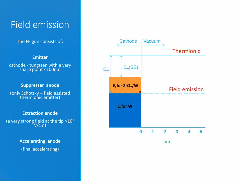
Field emission
The FE gun consists of:
Emitter
cathode - tungsten with a very sharp point <100nm
Suppresser anode
(only Schottky – field assisted thermionic emitter)
Extraction anode
(a very strong field at the tip >107
V/cm)
Accelerating anode
(final accelerating)
Thermionic
Field emissionEf for ZrO2/W
Ef for W
Cathode Vacuum
0 1 2 3 4 5
nm
EwEw(SE)


CENTER FOR ELECTRON MICROSCOPY AND MICROANALYSIS [email protected]
Schottky FEG
(Image: JEOL)
(Image: tnw.tudelft)
(Image: JEOL)
CENTER FOR ELECTRON MICROSCOPY AND MICROANALYSIS [email protected]
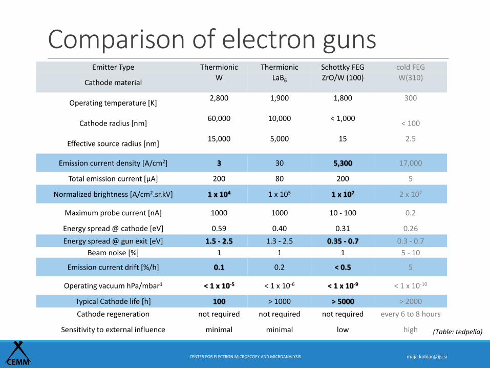
Comparison of electron gunsEmitter Type Thermionic Thermionic Schottky FEG cold FEG
Cathode material W LaB6 ZrO/W (100) W(310)
Operating temperature [K] 2,800 1,900 1,800 300
Cathode radius [nm] 60,000 10,000 < 1,000
< 100
Effective source radius [nm] 15,000 5,000 15 2.5
Emission current density [A/cm2] 3 30 5,300 17,000
Total emission current [µA] 200 80 200 5
Normalized brightness [A/cm2.sr.kV] 1 x 10⁴ 1 x 10⁵ 1 x 10⁷ 2 x 10⁷
Maximum probe current [nA] 1000 1000 10 - 100 0.2
Energy spread @ cathode [eV] 0.59 0.40 0.31 0.26
Energy spread @ gun exit [eV] 1.5 - 2.5 1.3 - 2.5 0.35 - 0.7 0.3 - 0.7
Beam noise [%] 1 1 1 5 - 10
Emission current drift [%/h] 0.1 0.2 < 0.5 5
Operating vacuum hPa/mbar1 < 1 x 10⁻⁵ < 1 x 10⁻⁶ < 1 x 10⁻⁹ < 1 x 10⁻¹⁰
Typical Cathode life [h] 100 > 1000 > 5000 > 2000
Cathode regeneration not required not required not required every 6 to 8 hours
Sensitivity to external influence minimal minimal low high
* virtual source; hPa= hectopascals = 100 Pa
(Table: tedpella)
CENTER FOR ELECTRON MICROSCOPY AND MICROANALYSIS [email protected]
Electromagnetic lens systemCondenser lens, objective lens and scanning coils.

CENTER FOR ELECTRON MICROSCOPY AND MICROANALYSIS [email protected]
EM lenses
(Images: ammrf)
Similar to glass lenses in optical microscopes.
Main role of EM lenses is to demagnify the source of electrons to form a much smaller diameter probe.
Two main lenses used in SEM:◦ Condenser lenses
◦ Objective lenses
CENTER FOR ELECTRON MICROSCOPY AND MICROANALYSIS [email protected]
EM lensesCONDENSER LENS
The main role of the condenser lens is to control the size of the beam and determines the number of electrons in the beam which hit the sample.
OBJECTIVE LENS
Focuses electrons on the sample at the working distance.
(Images: ammrf)

CENTER FOR ELECTRON MICROSCOPY AND MICROANALYSIS [email protected]
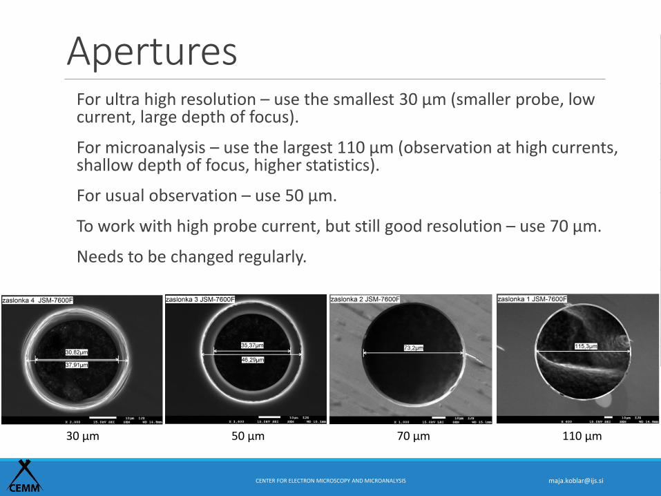
AperturesFor ultra high resolution – use the smallest 30 µm (smaller probe, low current, large depth of focus).
For microanalysis – use the largest 110 µm (observation at high currents, shallow depth of focus, higher statistics).
For usual observation – use 50 µm.
To work with high probe current, but still good resolution – use 70 µm.
Needs to be changed regularly.
30 µm 50 µm 70 µm 110 µm
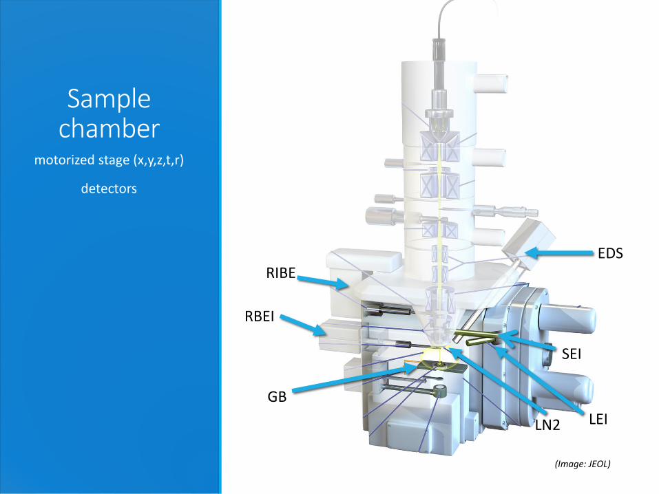
Sample chamber
motorized stage (x,y,z,t,r)
detectors
(Image: JEOL)
RIBE
RBEI
EDS
SEI
LEILN2
GB
CENTER FOR ELECTRON MICROSCOPY AND MICROANALYSIS [email protected]
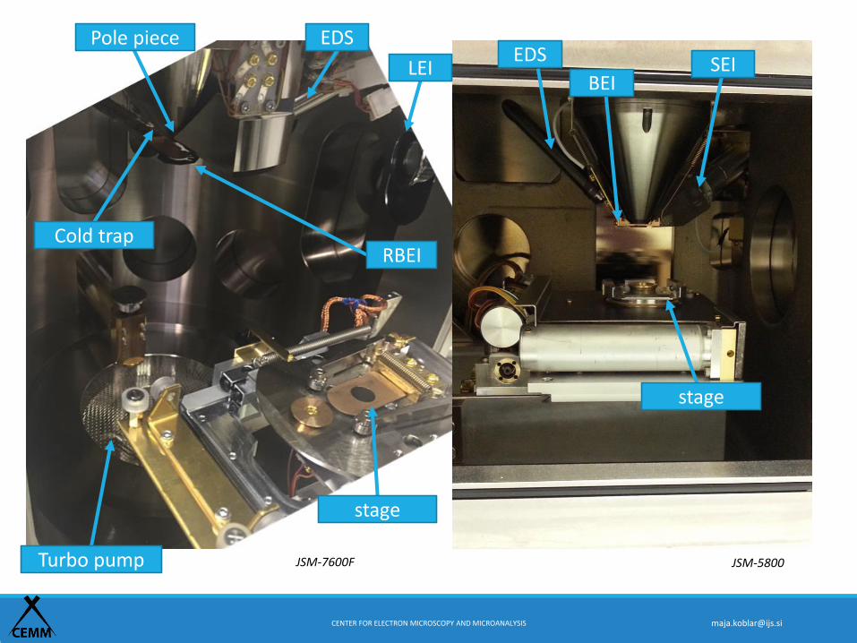
JSM-5800JSM-7600F
Pole piece
Cold trap
stage
LEI
Turbo pump
RBEI
EDS
BEISEI
EDS
stage
Electrons and their interactions
with the specimen
But we will not talk about excitation, we will talk about
ionization.

CENTER FOR ELECTRON MICROSCOPY AND MICROANALYSIS [email protected]
Interactions
Electrons:◦ Secondary (low energy)
◦ Backscattered (high energy)
◦ Transmitted
◦ Auger electrons
◦ Beam current
Photons
◦ X-rays
◦ cathodoluminescence
SEM
TEM
(Images: Low Voltage Electron Microscopy: Principles and Applications)
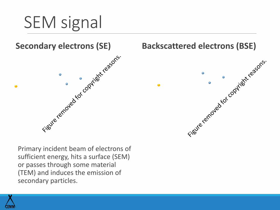
SEM signalSecondary electrons (SE) Backscattered electrons (BSE)
Primary incident beam of electrons of sufficient energy, hits a surface (SEM) or passes through some material (TEM) and induces the emission of secondary particles.
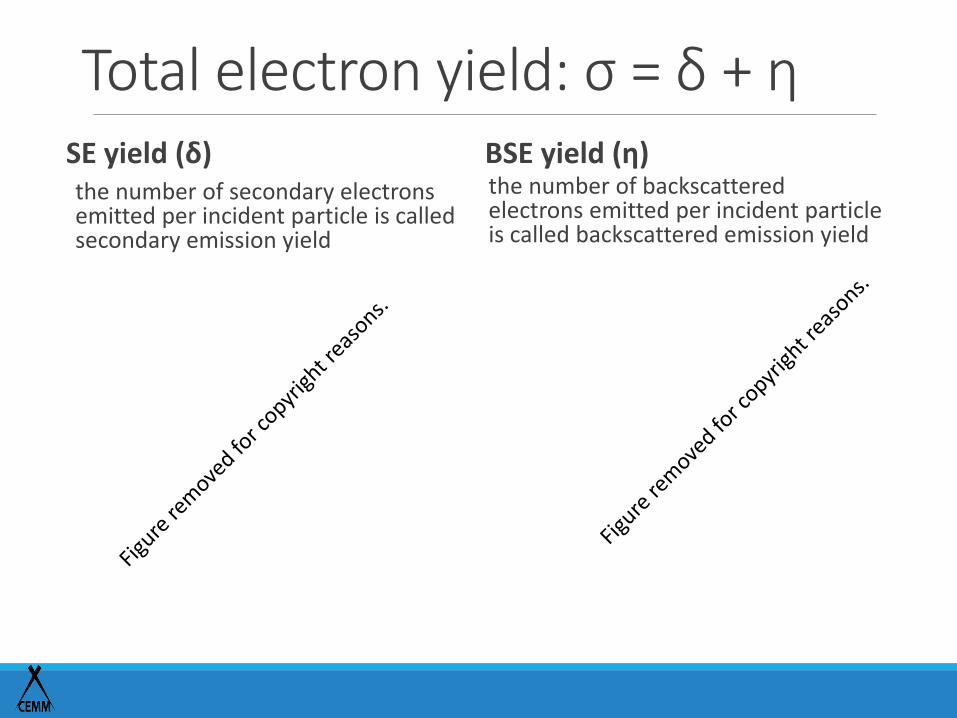
Total electron yield: σ = δ + ηSE yield (δ)the number of secondary electrons emitted per incident particle is called secondary emission yield
BSE yield (η)
phenomenon where primary incident particles
often refers to the emission of electrons when
the number of backscattered electrons emitted per incident particle is called backscattered emission yield
CENTER FOR ELECTRON MICROSCOPY AND MICROANALYSIS [email protected]
SignalSecondary electrons
◦ High resolution
◦ Strongly topography sensitive
◦ Little element sensitive
◦ Sensitive to charging
Backscattered electrons◦ Lower resolution
◦ Atomic number contrast in particular strong signal to heavy atoms
◦ Less sensitive to charging
CENTER FOR ELECTRON MICROSCOPY AND MICROANALYSIS [email protected]
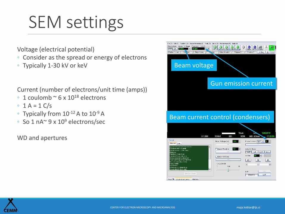
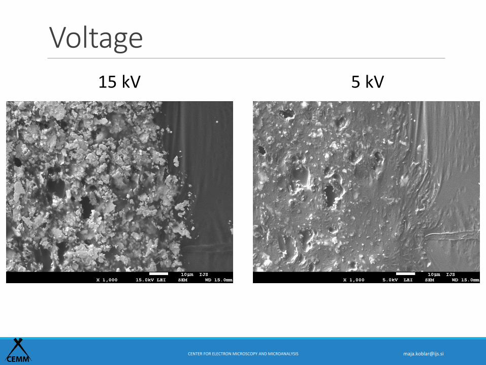
SEM settingsVoltage (electrical potential)◦ Consider as the spread or energy of electrons◦ Typically 1-30 kV or keV
Current (number of electrons/unit time (amps))◦ 1 coulomb ~ 6 x 10¹⁸ electrons◦ 1 A = 1 C/s◦ Typically from 10-12 A to 10-9 A◦ So 1 nA~ 9 x 10⁹ electrons/sec
WD and apertures
Beam voltage
Gun emission current
Beam current control (condensers)

CENTER FOR ELECTRON MICROSCOPY AND MICROANALYSIS [email protected]
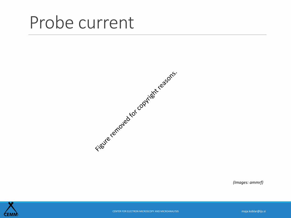
Probe current
PC 8 → 0,35 nA PC 6 → 0,08 nA
CENTER FOR ELECTRON MICROSCOPY AND MICROANALYSIS [email protected]
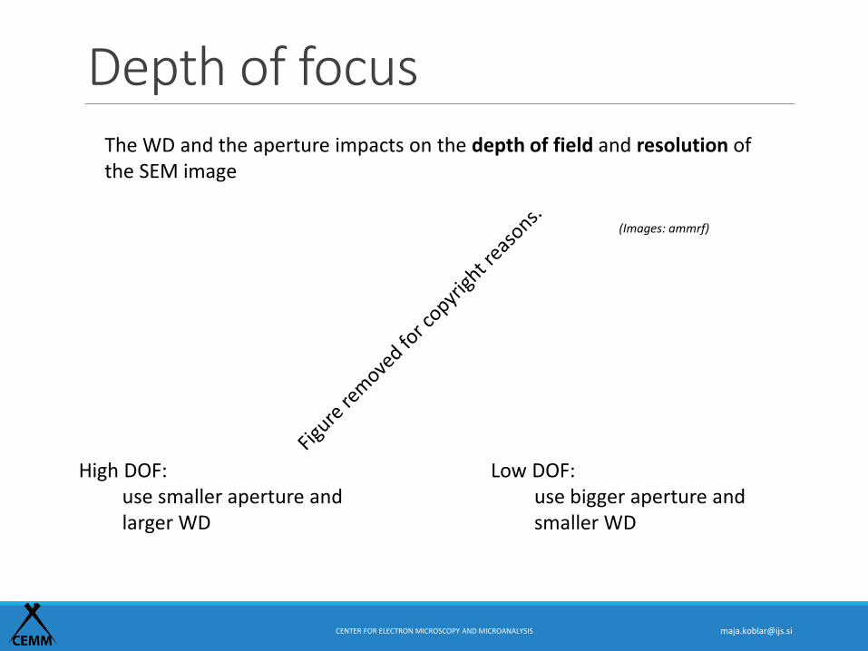
Depth of focus
(Images: ammrf)
The WD and the aperture impacts on the depth of field and resolution of the SEM image
High DOF:use smaller aperture and larger WD
Low DOF:use bigger aperture and smaller WD
CENTER FOR ELECTRON MICROSCOPY AND MICROANALYSIS [email protected]
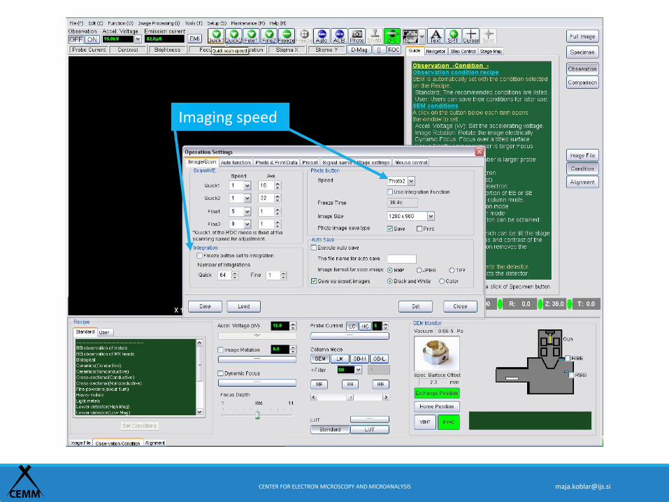
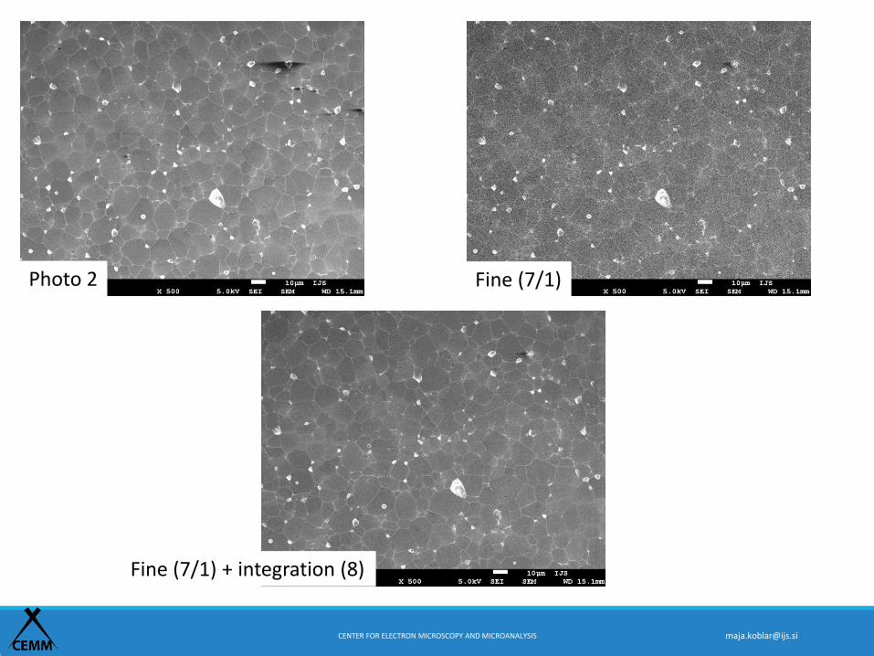
Photo 2 Fine (7/1)
Fine (7/1) + integration (8)
CENTER FOR ELECTRON MICROSCOPY AND MICROANALYSIS [email protected]
What is the working distance?
A. The seated distance between the microscopist and the microscope
B. The distance from the specimen to the secondary electron detector
C. The distance from the specimen to the objective lens pole piece
D. The distance from the specimen to X-ray detector
CENTER FOR ELECTRON MICROSCOPY AND MICROANALYSIS [email protected]
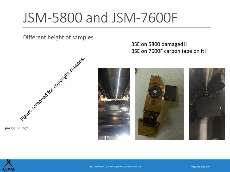
JSM-5800 and JSM-7600FDifferent height of samples
BSE on 5800 damaged!!BSE on 7600F carbon tape on it!!
(Image: ammrf)

CENTER FOR ELECTRON MICROSCOPY AND MICROANALYSIS [email protected]
Magnetic samplesA) minimal amount as possible!
◦ Bulk - less force
◦ Powder – to avoid flying of the holder
B) mount it very good! Use special holder
C) use slow movement (x, y and z) under the objective lens!◦ Turn on LM mode
◦ Be further away from the pol piece
D) focus, stigmatizm … very slowly!
CENTER FOR ELECTRON MICROSCOPY AND MICROANALYSIS [email protected]
Take home information• The SEM works differently than LM• But there are some similarities
• Why is it possible to image with electrons• The wave particle duality and the scanning mode makes it possible
• Different parts of the SEM and what is the difference between them • Why we have different types of electron gun (W, FE)• How the electromagnetic lenses work and why magnetic samples are a problem• Why we need Apertures • Detectors
• Electrons and their interactions with the specimen and what kind of information we get from SE and BSE image• SE yield• BSE yield
• SEM settings and how we observe it on the image• What is the difference in image depending on the
• Voltage
• Current
• WD and apertures
• Scanning speed

CENTER FOR ELECTRON MICROSCOPY AND MICROANALYSIS [email protected]
Next workshop on 7.8.2017:
- EDS,
- WDS,
- EBSD,


