
- 1 -
Root Locus Based, Integrated
Circuit Design of a Switch Mode,
Boost Current Regulator
By
Andy Radosevich (SJSU ID, Address,
Telephone, and Email
Removed for Privacy
December 17, 2010)
Approved
Advisor_____________________________________________
Professor Peter Reischl Date
Co-Advisor__________________________________________
Professor Morris Jones Date
Graduate Coordinator:
Professor Peter Reischl
©2009, 2010

- 2 -
MSEE Project
Submitted May 7, 2009
Corrected December 10, 2010: Typographical Errors and
Figures 13, 19, 22, and 31
Class, Term: EE297B, Fall 2008
Department of
Electrical Engineering
San Jose State University
San Jose, CA 95192

- 3 -
Abstract
Light emitting diode (LED) lighting is a new and growing application
for integrated circuits (ic’s) that control switch mode power supplies.
This project designs an ic that allows a switch mode power supply
(SMPS) to regulate current in an LED. This design uses the power
inductor dc resistance (DCR) to eliminate the need for a resistor to
sense the inductor current – a resistor that most comparable
commercial ic’s require. The design of the ic is based on an evaluation
of the Bode plots and root locus of the target power supply. A sub-
circuit within the ic allows soft-starting; and, logic inputs can turn off
the ic or change the amount of LED current. The efficiency for the
circuit that demonstrates ic operation is 85%.

- 4 -
Table of Contents
Abstract ...................................................................................................................................... - 3 -
Introduction ............................................................................................................................... - 5 -
Methodology............................................................................................................................... - 6 -
Literature Review...................................................................................................................... - 7 -
Specifications and Results......................................................................................................... - 8 -
Boost SMPS Basics .................................................................................................................. - 11 -
Demonstration Circuit........................................................................................................... - 11 -
Continuous and Discontinuous Conduction Mode (CCM and DCM) .................................. - 12 -
Methods of Feedback Control............................................................................................... - 14 -
Slope Compensation ............................................................................................................. - 16 -
Inductor DC Resistance (DCR) Current Sensing.................................................................. - 17 -
IC Functional Blocks ............................................................................................................ - 19 -
Basic Driver Design .............................................................................................................. - 22 -
Slope Compensation ............................................................................................................. - 23 -
Control-To-Output Transfer Functions ................................................................................. - 24 -
Feedback Loop Design ............................................................................................................ - 44 -
Ideal Amplifier Simulation ..................................................................................................... - 51 -
Transistor Level Design Detail ............................................................................................... - 54 -
Current Reference ................................................................................................................. - 55 -
Band-gap Reference.............................................................................................................. - 59 -
Shutdown Comparator .......................................................................................................... - 66 -
Regulator............................................................................................................................... - 68 -
Inductor DCR Current Sensing and Sense Amplifier ........................................................... - 72 -
Oscillator............................................................................................................................... - 79 -
Ramp Generator .................................................................................................................... - 84 -
Summer ................................................................................................................................. - 86 -
Error Amplifier Current Reference ....................................................................................... - 91 -
Error Amplifier ..................................................................................................................... - 93 -
Comparator............................................................................................................................ - 98 -
Soft-start Current Reference ............................................................................................... - 103 -
Gate Driver.......................................................................................................................... - 104 -
Summary and Conclusion..................................................................................................... - 106 -
Appendix A1: Basic Driver Design ..................................................................................... - 108 -
Appendix A2: Determine Average Equations.................................................................... - 109 -
Appendix A3: Perturb and Linearize Average Equations................................................ - 111 -
Appendix A4: Voltage Mode Boost Converter Control-to-Output Transfer Function .. - 113 -
Appendix A5: Simple CPM Boost Converter Control-to-Output Transfer Function ... - 115 -
Appendix A6: CPM with Slope Compensation Control-to-Output Transfer Function.. - 117 -
References .............................................................................................................................. - 123 -

- 5 -
Introduction
Integrated circuits (ic’s) that perform the primary power management or
control function in switch mode power supply (SMPS) circuits are called
power management ic’s. One of the latest applications of power
management ic’s is in the area of light emitting diode (LED) lighting.
Examples of LED lighting are: the back-light on your cell phone or laptop
display, and the tail, instrument, and interior lights of the latest automobiles.
LEDs will outperform and consequently replace most incandescent and other
types of light sources in the near future [1] Tsao, 2003. Tsao wrote in Laser
Focus World that
“During the next five to ten years semiconductor-based solid-state
lighting (SSL) is expected to outperform first incandescence, then
fluorescence and high-intensity discharges (HID), for general
illumination” [1] Tsao, 2003.
LEDs also have a long expected life. A Diamond Dragon LED from Osram
Opto Semiconductor Gmbh can have a life of 50,000 hours or more [2]
Osram, 2008.
Power management ic’s that are used in switch mode power supplies for
LED lighting already exist, and more are currently being developed. The
power management ic’s that are used in LED lighting are similar to those
used in dc-dc power supply circuits. The power management ic’s in dc-dc
power supply circuits regulate the output voltage, but in a power supply
circuit for LEDs, LED current is regulated instead.
There are several different SMPS topologies and many texts explain their
operation: [3] Mohan, 2007, [4] Erickson, 1997, and [5] Brown, 1994. Each
topology can be configured to regulate the output current, so each can be
used for LED lighting. A power supply circuit where the input voltage is
higher than the output voltage is called a buck regulator. Boost regulators
have an input voltage that is less than the output voltage.
This project designs the ic portion of a SMPS that boosts a dc input voltage
to a higher output voltage, and regulates the output dc current. The ic is
called a boost SMPS current regulator controller, and is appropriate for LED
lighting circuits.

- 6 -
Methodology
This project designs a boost SMPS current regulator controller ic. A
literature review is performed to establish the significance of the project in
relation to the state-of-the-art. The control-to-output transfer function (TF)
for the system is determined, and then used to design the feedback loop
compensation so the system is stable. Then the system is implemented both
by using ideal amplifiers, and at the transistor level.
This report discusses these SMPS basics before deriving the control-to-
output transfer function:
• demonstration circuit
• continuous conduction mode (CCM) and discontinuous conduction
mode (DCM)
• methods of feedback control
• slope compensation
• inductor DC resistance (DCR) current sensing
• ic functional blocks
The control-to-output transfer function is derived and used for stability
analysis. The control-to-output transfer function is derived for a method of
feedback control that is called current programmed mode (CPM) with slope
compensation [4] Erickson, 1997. The control-to-output transfer function is
also derived for two other methods of feedback control for comparison:
voltage mode and simple CPM. The control-to-output transfer functions are
checked for accuracy by comparisons to SwitcherCad© (SPICE)
simulations.
Switch mode power supplies require feedback, and compensation is
necessary to make the feedback loop stable. Compensation is designed
using the control-to-output transfer function combined with Bode and root
locus plots. The entire SMPS circuit with compensation is simulated to
evaluate operation and stability, first using ideal amplifiers and with the
circuit designed at the transistor level. The transistor level design is
detailed.

- 7 -
Literature Review
Table 1 shows the ic that is designed for this project, and two comparable
commercial ic’s. All three ic’s have similar functionality for shut-down,
quiescent input current, soft-start, and control mode. The commercial ic’s
have functions that this ic does not: wide Vin range, variable switching
frequency, analog or pulse width modulation (pwm) LED dimming, and
high-side sensing of the LED current. The ic designed for this project uses
the power inductor dc resistance (DCR) to eliminate the need for a resistor to
sense the inductor current. The commercial ic’s require a resistor to sense
inductor current.
Comparison of IC’s
Manufacturer
Part
Number Pins
Vin
Range
Switching
Frequency
Shut-
down
Quiescent
Input
Current
(not
switching)
LED
Dimming
High
Side
Current
Sense
Switch
Current
Limit
Soft
Start
(V) (MHz) (mA)
Linear LT3755 16+EP* 4.5 - 40
100kHz -
1MHz yes 1.5
analog or
pwm** yes
External
R
External
C
Maxim MAX16834 20+EP* 4.75 - 28
100kHz -
1MHz yes 6
analog or
pwm** yes
External
R
External
C
This Project 10+EP* 3 - 5.6 400kHz yes 2 logic no
Inductor
DCR
External
C
* EP = Exposed Pad
** pwm = pwm dimming Table 1: This table shows the ic that is designed for this project, and two comparable
commercial ic’s. The ic designed for this project uses the power inductor dc resistance
(DCR) to eliminate the need for a resistor to sense the inductor current. The commercial
ic’s require a resistor to sense inductor current.

- 8 -
Specifications and Results
Table 2 shows the specifications and results for this project. The
specifications are re-iterated from table 1, except this table includes a
specification for efficiency. Simulations are used to determine the results,
and they show that the ic designed for this project meets the specifications.
Specifications for the Proposed IC and Results
Pins
Vin
Range
Switching
Frequency
Shut-
down
Quiescent
Input
Current
(not
switching)
LED
Dimming
Switch
Current
Limit
Soft
Start
Control
Mode
Effici-
ency
(V) (MHz) (mA)
Specifi-
cation 10+EP* 3 - 5.6 400kHz yes 2 logic
Inductor
DCR
External
C
Current
Mode 0.85
Results 10+EP* 3 - 5.6 400kHz yes 2 logic
Inductor
DCR
External
C
Current
Mode 0.85
* EP =
Exposed
Pad
Table 2: This table shows the specifications and results for this project. The
specifications are re-iterated from table 1, except this table includes a specification for
efficiency. Simulations were used to determine the results, and they show that the ic
designed for this project meets the specifications.
The ic designed for this project is simulated in figure 1. The ic is designed
at the transistor level for the simulation. The simulation shows that the
transistor level design of the ic for the project meets several of the
specifications, and the control system for the design is stable:
• The circuit starts up under soft-start control when Vin is first applied,
but also soft-starts if the logic input for shutdown causes a re-start.
• A logic input changes the LED current.
• The circuit has a critically damped transient response, so the system is
stable.

- 9 -
Figure 1: This figure is a waveform that shows the results of the transistor level design
simulation. The simulation shows that the circuit starts up under soft-start control when
Vin is first applied, but also soft-starts if the logic input for shutdown causes a re-start.
The simulation also shows that a logic input can change the LED current, and the system
is stable.
Figure 2 shows the top level of the schematic that is used for the transistor
level design simulation.
Force Re-start
– Soft-starts
LED Current
Force Transient
- Stable
Regulates at 300mA Logic Input for Shutdown (Voltage)
Current Command
Transistor Level Design Simulation – Start Up
Cu
rre
nt

- 10 -
Figure 2: This figure shows the top level of the schematic that is used for the transistor level design simulation.
Transistor Level Design, Top Level Schematic

- 11 -
Boost SMPS Basics
This project designs a boost SMPS current regulator controller ic. The
control-to-output transfer function is derived after discussion of these SMPS
basics:
• demonstration circuit
• continuous conduction mode (CCM) and discontinuous conduction
mode (DCM)
• methods of feedback control
• slope compensation
• inductor dc resistance (DCR) current sensing
• ic functional blocks
Demonstration Circuit
Figure 3 is a boost SMPS current regulator circuit that uses this project’s
proposed power management ic design. The circuit takes an input of 3 -
5.6Vdc from three or four nickel-metal hydride (NiMH) cells, and boosts the
output voltage to about 6.75Vdc to power two LEDs in series. The output
voltage is called the LED voltage. The LED voltage is the voltage from the
anode of the LED at the highest voltage in the LED string to the cathode of
the LED in the string at the lowest voltage. The LED voltage will change as
the LEDs temperature-stabilize. The LED current will remain regulated at
300mA.
As also shown in figure 3, the boost SMPS current regulator circuit consists
of the power management ic, input capacitor, inductor, switching MOSFET
M1 (switch), diode, and output capacitor. The switch current is sensed using
the dc resistance (DCR) of the 22uH inductor. The LED current is sensed
using the 0.3 ohm resistor. The switching frequency fsw is 400kHz. There
are many texts such as [3] Mohan, 2007, [4] Erickson, 1997, and [5] Brown,
1994 that explain the operation of boost SMPS circuits. The operation of a
circuit that regulates the LED current is exactly the same, except the output
current is regulated, instead of the output voltage.

- 12 -
Figure 3: This is a boost SMPS current regulator circuit that uses this project’s proposed
power management ic design. The switching MOSFET M1 (switch) current is sensed
using the dc resistance (DCR) of the 22uH inductor. The LED current is sensed using the
0.3 ohm resistor. The switching frequency fsw is 400kHz.
Continuous and Discontinuous Conduction Mode (CCM and DCM)
A SMPS regulator circuit can operate in either continuous conduction mode
(CCM) or discontinuous conduction mode (DCM). The analysis for this
report is done for CCM operation, particularly in the area of stability
analysis. A similar method can be used for DCM analysis. As explained in
[3] Mohan, 2007, [4] Erickson, 1997, and [5] Brown, 1994 and many other
places, SMPS regulator circuits operate by turning the switch on and off at
the switching frequency. The time the switch is on plus the time the switch
is off is called the switching period (T). The switching frequency is 1/T. In
CCM there are two states during T, and in DCM there are three states.
In CCM, there are two switching states during T, and the current in the
inductor never becomes zero. In CCM operation, T is composed of a state
M1
Boost SMPS Current Regulator

- 13 -
when the switch is on and a state when the switch is off, for a total of two
states. In CCM, current continues to flow in the inductor during both states.
In DCM operation, T is composed of three states. There are states when the
switch is on and the switch is off and current continues to flow in the
inductor, just as for CCM operation. But, there is a third state in which the
switch is off, and there is no current flowing in the inductor.
The inductor current is composed of an average or dc component, plus a
time-varying component that is called the inductor ripple current. If half the
inductor ripple current becomes larger than the average inductor current, the
SMPS regulator will transition from CCM to DCM operation, as shown in
figure 4.
In figure 4, the middle inductor current waveform is at the continuous
conduction mode/discontinuous conduction mode (CCM/DCM) border,
because half the inductor ripple current is equal to the average inductor
current. The top inductor current waveform shows CCM operation and the
bottom waveform shows DCM operation. When the inductor current
approaches zero, the diode in figure 3 causes the inductor current to remain
at zero, rather than flow backwards. The zero inductor current causes the
third switching state for DCM operation.

- 14 -
Figure 4: The middle inductor current waveform is at the continuous conduction
mode/discontinuous conduction mode (CCM/DCM) border, because half the inductor
ripple current is equal to the average inductor current. The top inductor current
waveform shows CCM operation and the bottom waveform shows DCM operation.
Methods of Feedback Control
A power supply uses feedback, so it is a control system. Feedback keeps the
output of a voltage or current regulator from changing, even though the input
voltage or output load may change. This section introduces three types of
Ind
uct
or
Cu
rren
t (A
)
t (ms)
½ Inductor Ripple Current =
Inductor DC Current =>
Borderline CCM/DCM
DCM
CCM
CCM and DCM Waveforms

- 15 -
feedback control. The control-to-output transfer functions that are derived
later and used for stability analysis depend on the type of feedback control.
Switch mode power supplies usually use either voltage mode control or peak
current mode control [3] Mohan, 2007. Peak current mode is also called
current programmed mode (CPM) [4] Erickson, 1997. There are two ways
to analyze CPM control: simple CPM or CPM with slope compensation.
The difference between simple CPM and CPM with slope compensation will
be discussed later.
Switch mode power supplies with voltage mode control have a single
feedback loop. The difference between the output voltage and a reference
produces an error voltage, and the error voltage controls the duty cycle [4]
Erickson, 1997. Figure 5 is a block diagram for a SMPS with voltage mode
control. There are several gain blocks: the controller, the pulse width
modulator, the power stage, and the feedback attenuation. The
compensation that is contained within the controller ensures that the control
system is stable.
SMPS with Voltage Mode Control
Figure 5: This block diagram for a SMPS with voltage mode control shows a single
feedback loop. [4] Erickson, 1997.
Switch mode power supplies with either type of CPM control have two
feedback loops: an inner and an outer control loop [4] Erickson, 1997. The
outer loop again consists of several gain blocks: the controller, the CPM
controller, the power stage, and the feedback attenuation. The inner control
loop is within the CPM controller [4] Erickson, 1997. The inner loop
controls the peak inductor current according to a reference from the outer

- 16 -
control loop. The outer control loop produces a reference that indicates how
much current is required from the power inductor to regulate the output
voltage. The error amplifier in the outer control loop compares the output
voltage to a reference. Figure 6 is a block diagram that shows the inner and
outer control loops of a CPM control SMPS. When the power supply uses
an inner loop to control inductor current, the inductor can be treated as a
current source controlled by a reference from the outer control loop [4]
Erickson, 1997. This removes the inductor from the transfer function of the
power stage, and simplifies the compensation.
The inner control loop controls the inductor current by turning on and off the
switch. When the reference from the outer control loop requests more
inductor current, the switch stays on a longer portion of the switching cycle.
When less inductor current is requested, the switch stays on a shorter
portion. The switch always turns on once each switching cycle. How long it
stays on is determined by the relationship between the reference from the
outer current control loop, and the inductor current that is sensed.
CPM Control - Inner and Outer Control Loops
Figure 6: This is a block diagram that shows the inner and outer control loops of a CPM
control boost SMPS [4] Erickson, 1997.
Slope Compensation
Slope compensation is necessary to make the inner current control loop of
the CPM boost converter stable when the duty cycle D is greater than 0.5 [4]
Erickson, 1997. The duty cycle is the ratio of the time the switch is on
during switching period, compared to the switching period. Slope
compensation can be performed by adding a ramp voltage to the signal that

- 17 -
represents the inductor current [4] Erickson, 1997. The sum of the ramp
voltage and the inductor current signal is then used by the inner current
control loop. Slope refers to the steepness of the ramp voltage.
[4] Erickson, 1997 and [6] Bruzos, 1989 explain slope compensation and
why it stabilizes the inner control loop for D > 0.5. According to [4]
Erickson, 1997, the correct amount of slope compensation results in a value
of α that is less than 1 for worst case operating conditions. Worst case
operating conditions for the boost converter in terms of slope compensation
are at minimum input voltage Vg and maximum output voltage V. Ma is the
amount of slope compensation referenced to the inductor current in A/s.
From [4] Erickson, 1997:
Inductor DC Resistance (DCR) Current Sensing
The inner control loop senses the inductor current across the inductor DCR.
Inductor current can also be sensed by placing a current sense resistor in
series with the switch. It is preferable to sense the current at the inductor
because it eliminates the need for a sense resistor. The voltage across the
inductor has a switching component and a ‘current multiplied by resistance’
(I*R) component. The switching component of the inductor voltage is large
with relatively fast transitions compared to the I*R component. The
inductor has the input voltage Vg across it during one part of the switching
cycle, and it has the input minus the output voltage Vg-V across it during the
other part. Again, the analysis of this report is for CCM operation. The I*R
component of the inductor voltage is smaller with slower transitions. It
occurs because the current in the inductor ramps up and down during the
switching cycle and creates a corresponding voltage across the inductor
DCR. To extract the DCR voltage from the switching voltages, the inductor
voltage is put through a low pass filter [7] Zhang, 2008. Figure 7 shows the
voltage across the inductor and the voltage across the inductor DCR caused
by the inductor current.
MaL
Vg
MaL
VgV
+
−−
=α

- 18 -
Figure 7: This figure shows the voltage across the inductor and the voltage across the
inductor DCR caused by the inductor current. The inductor has the input voltage Vg
across it during one part of the switching cycle, and it has the input minus the output
voltage Vg-V across it during the other part.
Ind
uct
or
DC
Res
ista
nce
(D
CR
)
Vo
ltag
e (m
V)
Ind
uct
or
Vo
ltag
e (V
)
Vg
Vg-V
Inductor DCR Voltage and Inductor Voltage
- 19 -
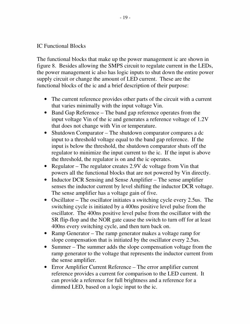
IC Functional Blocks
The functional blocks that make up the power management ic are shown in
figure 8. Besides allowing the SMPS circuit to regulate current in the LEDs,
the power management ic also has logic inputs to shut down the entire power
supply circuit or change the amount of LED current. These are the
functional blocks of the ic and a brief description of their purpose:
• The current reference provides other parts of the circuit with a current
that varies minimally with the input voltage Vin.
• Band Gap Reference – The band gap reference operates from the
input voltage Vin of the ic and generates a reference voltage of 1.2V
that does not change with Vin or temperature.
• Shutdown Comparator – The shutdown comparator compares a dc
input to a threshold voltage equal to the band gap reference. If the
input is below the threshold, the shutdown comparator shuts off the
regulator to minimize the input current to the ic. If the input is above
the threshold, the regulator is on and the ic operates.
• Regulator – The regulator creates 2.9V dc voltage from Vin that
powers all the functional blocks that are not powered by Vin directly.
• Inductor DCR Sensing and Sense Amplifier – The sense amplifier
senses the inductor current by level shifting the inductor DCR voltage.
The sense amplifier has a voltage gain of five.
• Oscillator – The oscillator initiates a switching cycle every 2.5us. The
switching cycle is initiated by a 400ns positive level pulse from the
oscillator. The 400ns positive level pulse from the oscillator with the
SR flip-flop and the NOR gate cause the switch to turn off for at least
400ns every switching cycle, and then turn back on.
• Ramp Generator – The ramp generator makes a voltage ramp for
slope compensation that is initiated by the oscillator every 2.5us.
• Summer – The summer adds the slope compensation voltage from the
ramp generator to the voltage that represents the inductor current from
the sense amplifier.
• Error Amplifier Current Reference – The error amplifier current
reference provides a current for comparison to the LED current. It
can provide a reference for full brightness and a reference for a
dimmed LED, based on a logic input to the ic.

- 20 -
• Error Amplifier - The error amplifier is a trans-conductance amplifier
with inputs that compare the error amplifier current reference to the
LED current. The error amplifier and the resistor capacitor (RC)
network at the output of the error amplifier compensate the feedback
loop. The RC makes a compensation zero. The output resistance of
the trans-conductance amplifier and the C make a compensation pole.
The error amplifier trans-conductance gm and output resistance rO
determine the dc gain of the sense amplifier. The error amplifier also
has a gain-bandwidth product (GBW) that adds a pole to the
compensation.
• Comparator - The comparator compares the output of the error
amplifier to the output of the summer to determine when to turn the
switch off. If the comparator does not turn the switch off, the
oscillator will turn the switch off for 400ns and then turn it back on.
• Soft-start Current Reference – The soft-start current reference charges
the soft-start capacitor when the shutdown comparator allows the ic to
operate. The soft-start capacitor clamps the output of the error
amplifier to prevent over-shoot of the inductor current during start-up.
Without soft-start, the inductor current may overshoot during start-up
when the input supply voltage is first applied to the circuit, or the
logic input to the ic for shutdown changes from low to high.
• Gate Driver – The gate driver interfaces the output of the NOR gate to
the gate of the switching MOSFET.

- 21 -
Figure 8: These are the functional blocks that make up the boost SMPS current regulator
power management ic.
Controller
IC
Error
Amp
Shutdown
Comparator
Summer
Error Amp
Current
Reference
Current
Reference
Soft-Start
Current
Reference
Regulator
Gate
Driver
Band Gap
Reference
Sense Amp
IC Functional Blocks

- 22 -
Control-to-Output Transfer Function
The control-to-output transfer function is derived for a boost SMPS, and
then used for stability analysis. The control-to-output transfer function is
derived for current programmed mode (CPM) control with slope
compensation, but for comparison the control-to-output transfer function is
also derived for voltage mode control and simple CPM control. The control-
to-output transfer functions are checked for accuracy by comparisons to
SwitcherCad simulations. This section analyzes a boost converter that
regulates voltage, although the final compensation design, after the analysis,
is for a boost current regulator.
First a basic driver design is performed to select the inductor, input
capacitor, and output capacitor values, based on the operating conditions.
The basic driver design values are used in the analysis of the three types of
control for the boost SMPS: voltage mode, simple CPM, and CPM with
slope compensation. The amount of slope compensation that is required is
also determined. Slope compensation is not required for the voltage mode or
simple CPM control analysis. Then the control-to-output transfer functions
are found for all three control types. The Bode plots from the transfer
functions are compared to Bode plots from SwitcherCad simulations. The
root locus for each of the transfer functions is also determined.
Basic Driver Design
Table 3 shows the operating conditions that were used to perform the basic
driver design. Figure 9 shows the schematic for the basic driver design. The
inductor, input capacitor, and output capacitor are the result of the basic
driver design performed in Appendix A1.

- 23 -
Operating Conditions for Basic Driver Design
Input
Voltage Vg
Output
Voltage V
fsw Rload Conduction
Mode
3.375V 6.75V 400kHz 22.5 ohms CCM
Table 3: This table shows the operating conditions used for the basic driver
design.
Figure 9: This figure shows the basic driver design. The inductor, input capacitor, and
output capacitor are the result of the basic driver design performed in Appendix A1.
Slope Compensation
CPM with slope compensation control requires a specific value of slope
compensation. Simple CPM control does not require slope compensation for
analysis, but the assumption is made that the inner control loop is stable for
all values of duty cycle. Slope compensation is not required for voltage
mode control.
Worst case operating conditions for the boost converter in terms of slope
compensation are at minimum input voltage Vg and maximum output
voltage V. The inductance value chosen for this design is 22µH, but 10µH is
Circuit for Basic Driver Design

- 24 -
used in the slope compensation calculation to add margin. From [4]
Erickson, 1997:
Mam
Mam
+
−=
1
2α
Set 1=α and use worst case Vg, V, and L:
sAMa
Mae
Mae /120000108000
610
3610
316.8
1 =⇒=
+−
−−
−
=
Control-To-Output Transfer Functions
There are up to five steps to find the control-to-output transfer function for
the types of SMPS control discussed in this report. The first two steps are
necessary for all three types of control: voltage mode, simple CPM, and
CPM with slope compensation. The last three steps are only required to find
the control-to-output transfer function for CPM with slope compensation
control. The approach from [4] Erickson, 1997 is used here. The five steps
are:
1. determine the averaged equations
2. perturb and linearize the average equations
3. use the control law
4. make a y-parameter model
5. use the y-parameter model to find the control-to-output TF
The first step to find the control-to-output transfer function for all three
types of SMPS control is to determine the average equations. First the
voltage and current equations for the inductor and capacitor are determined.
Also, the input voltage vg(t) and the output voltage v(t) are replaced with
their low frequency averaged values according to the small ripple
approximation [4] Erickson, 1997. Starting with figure 9, the driver is
divided into two circuits: one when the switch is on, and one when the
switch is off. Figure 10 is the circuit when the switch is on.

- 25 -
Boost Circuit When the Switch is On
Figure 10: This is the circuit used to determine the voltage and current equations for the
inductor and capacitor, when the switch is on.
Figure 11 is the circuit when the switch is off.
Boost Circuit When the Switch is Off

- 26 -
Figure 11: This is the circuit used to determine the voltage and current equations for the
inductor and capacitor when the switch is off.
The average equations are determined in appendix A2. These are the
average equations for the inductor, capacitor, and input current from
appendix A2:
TTg
TLtvtdtv
dt
tidL )()(')(
)(−=
TT
T
R
tvtitd
dt
tvdC
)()()('
)(−=
TTg titi )()( =
Next the equations for the boost converter averaged equations are perturbed
and linearized as shown in appendix A3. These are the perturbed and
linearized averaged equations from appendix A3:
• Inductor
)()(')()( ^^^
^
tdVtvDtvdt
tidL g +−=
• Capacitor
)(1
)()(')( ^^^
^
tvR
ItdtiDdt
tvdC −−=
• Input Current
)()(^^
titi g =
These familiar dc relations for a boost converter are also derived in appendix
A3:

- 27 -
'D
VgV =
'IDR
V=
IIg =
Figure 12 is the small signal model that represents the perturbed and
linearized averaged equations from above for the inductor voltage, capacitor
current, and input current [4] Erickson, 1997. The model is the first step to
find the control-to-output transfer function of the voltage mode boost SMPS.
Voltage Mode Control Small Signal Model
Figure 12 is the small signal model that represents the perturbed and linearized averaged
equations for the inductor voltage, capacitor current, and input current [4] Erickson,
1997.
The control-to-output transfer function of the voltage mode boost SMPS is
determined in appendix A4, and is shown here:
( ) ( )'
''1
'1
0)(^)(
)()(
2
22
^
^
D
V
sD
LCs
DR
L
sVD
IL
sgvsd
svsGvd
++
−
=
=
=
Note there is a zero in the right hand plane (RHP). Both the closed and open
loop transfer functions of a power supply contain poles and zeros. The

- 28 -
location of the closed loop poles of the transfer function start at the open
loop poles and move to the open loop zeros as the gain in the feedback path
goes from zero to infinity [8] Kuo, 1991. The path of the closed loop poles
as they move is called the root locus. The root locus of a system indicates if
the system is stable for a particular gain in the feedback, and also how close
the system is to becoming unstable [8] Kuo, 1991.
The open loop transfer function of a boost SMPS has a zero in the right-hand
plane (RHP) [3] Mohan, 2007. When the closed loop poles of the boost
SMPS transfer function move from the open loop poles to the open loop zero
in the RHP, the system becomes unstable [8] Kuo, 1991. The choice of
functional blocks and compensation for this design prevents instability
caused by the RHP zero.
Figures 13 and 14 are the root locus and Bode plot for the voltage mode
boost converter. The values from the basic driver design of figure 9 and the
operating conditions from table 3 are used. The figure 13 root locus shows
the RHP zero that occurs for all three models, and the locations of the poles
and zeros.

- 29 -
Figures 13: This figure shows the root locus for the voltage mode boost converter using
the basic driver design of figure 9 and the operating conditions from table 3. The root
locus shows the RHP zero that occurs for all three control methods, and the locations of
the poles and zeros.
X105
Root Locus for Voltage Mode
104(-0.4728 +
4.8943i)
rads/sec
2.5568(105)
rad/sec
104 (-0.4728 -
4.8943i)
rads/sec

- 30 -
Figures 14: This figure is the Bode plot for the boost SMPS with voltage mode control
using the values from the basic driver design of figure 9 and the operating conditions
from table 3.
Compensating the voltage mode boost SMPS is relatively difficult, based on
the Bode plot. The compensation must boost the open loop phase by over 90
degrees at the gain crossover frequency. Greater than 90 degrees of boost
requires two poles and two zeros. From control theory, the open loop phase
must remain above 180 degrees at frequencies below the crossover
frequency [8] Kuo, 1991. This includes the 90 degrees of phase that is due
to the integrator in the compensation. The integrator increases the order of
the system and makes the steady state error equal zero [3] Mohan 2007.
The transfer function that was derived for the voltage mode boost SMPS can
be checked by comparing Bode plots based on the transfer function to Bode
plots from SwitcherCad simulations. Figure 15 is the circuit that is used for
both the voltage mode simulation and the simulation of simple CPM control
in the next section [9] Erickson and Maksimovic, 2003. Figure 16 shows the
sub-circuit detail that implements the average switch model [9] Erickson and
Bode Plot for Voltage Mode

- 31 -
Maksimovic, 2003. The average switch model replaces the switch and diode
in the boost circuit to make the model continuous [9] Erickson and
Maksimovic, 2003. When the model is continuous, an ac analysis is
performed in SwitcherCad to get the Bode plot. Figure 17 is the Bode plot
for the simulated voltage mode boost converter. The plot is similar to the
Bode plot based on the transfer function in figure 14, so the transfer function
was derived correctly.
Simulation Circuit for Voltage Mode and Simple CPM Control
Figure 15: This is the circuit that is used for both the voltage mode simulation and the
simulation of the simple CPM model in the next section [9] Erickson and Maksimovic,
2003.

- 32 -
Average Switch Sub-Circuit Detail
Figure 16: This figure shows the sub-circuit detail that implements the average switch
model. [9] Erickson and Maksimovic, 2003.

- 33 -
Voltage Mode Control Simulation Bode Plot
Figure 17: This figure is the Bode plot for the simulated voltage mode boost SMPS. The
plot is similar to the Bode plot based on the transfer function in figure 14, so the transfer
function was derived correctly.

- 34 -
Three points have already been made about CPM Switch mode power
supplies:
1. There are two feedback loops: an inner and an outer control loop.
2. Slope compensation is necessary to keep the inner control loop stable.
3. When the power supply uses an inner loop to control inductor current,
the inductor can be treated as a current source controlled by a
reference from the outer control loop [4] Erickson, 1997.
Analysis for the simple CPM control boost SMPS makes the assumption that
the inductor current is the same as the reference from the outer control loop,
which is called the control current. The control-to-output transfer function
of the simple CPM control boost SMPS is derived in appendix A5.
First from appendix A5, this is the equation that describes the CPM boost
equivalent circuit using the simplified model:
'
1)(
1)(
1)(
'1')()(
^^^
2
^^
RDsgv
Rsv
Rsv
RD
sLDsicsvsC +−−
−≈
The above equation is used to draw Figure 18 which is the ac equivalent
circuit for the boost SMPS using simple CPM control [4] Erickson, 1997:
Simple CPM Mode Control Small Signal Model
Figure 18: This is the ac equivalent circuit for the boost SMPS using simple CPM
control [4] Erickson, 1997.
Now use Figure 18 to find the control-to-output transfer function:

- 35 -
−=
=
= RCs
RRD
sLD
sgvsic
svsGvc //
1//
'1'
0)(^)(
)()(
2^
^
12
'1
2'
2
+
−
=RCs
RD
sL
RD
Figures 19 and 20 are the root locus and Bode plot for the boost SMPS with
simple CPM control, using the basic driver design of figure 9 and the
operating conditions from table 3.
Figures 19: This figure is the root locus for the boost SMPS with simple CPM control,
using the basic driver design of figure 9 and the operating conditions from table 3.
-1.8913(104)
rads/sec
2.5568(105)
rad/sec
x 105
Root Locus for Simple CPM Control

- 36 -
Figures 20: This figure is the Bode plot for the boost SMPS with simple CPM control
using the basic driver design of figure 9 and the operating conditions from table 3.
The boost SMPS with simple CPM control is relatively easy to compensate,
based on the Bode plot. The compensation must boost the open loop phase
by 90 degrees or less at the crossover frequency. If the required phase boost
is less than 90 degrees, only a single pole and a single zero are required.
From control theory, the open loop phase must remain above 180 degrees at
frequencies below the crossover frequency, including 90 degrees of phase
that is due to the integrator already mentioned.
The transfer function that was derived for the boost SMPS with simple CPM
control can be checked by comparing Bode plots based on the transfer
function to Bode plots from SwitcherCad simulations. The simulation uses
the same circuits in Figures 15 and 16 that were used for the voltage mode
Bode Plot for Simple CPM Control

- 37 -
simulation. Instead of plotting the ac analysis of the output voltage V(3) in
SwitcherCad, the ac analysis of the output voltage with respect to the
inductor current V(3)/I(L1) is plotted instead. Figure 21 is the Bode plot for
the simulated boost SMPS with simple CPM control. The plot is similar to
the Bode plot based on the transfer function in figure 20, so the transfer
function was derived correctly.
Simple CPM Control Simulation Bode Plot
- 38 -
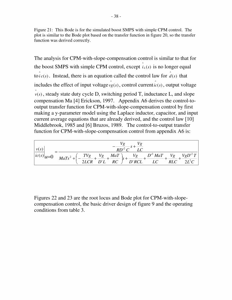
Figure 21: This Bode is for the simulated boost SMPS with simple CPM control. The
plot is similar to the Bode plot based on the transfer function in figure 20, so the transfer
function was derived correctly.
The analysis for CPM-with-slope-compensation control is similar to that for
the boost SMPS with simple CPM control, except )(^
si L is no longer equal
to )(^
sci . Instead, there is an equation called the control law for )(^
sd that
includes the effect of input voltage )(^
svg , control current )(^
sic , output voltage
)(^
sv , steady state duty cycle D, switching period T, inductance L, and slope
compensation Ma [4] Erickson, 1997. Appendix A6 derives the control-to-
output transfer function for CPM-with-slope-compensation control by first
making a y-parameter model using the Laplace inductor, capacitor, and input
current average equations that are already derived, and the control law [10]
Middlebrook, 1985 and [6] Bruzos, 1989. The control-to-output transfer
function for CPM-with-slope-compensation control from appendix A6 is:
CL
TVgD
RLC
Vg
LC
MaTD
RCLD
Vgs
RC
MaT
LD
Vg
LCR
TVgMaTs
LC
Vgs
CRD
Vg
sic
sv
u2
232
2
2
''
''2
'
)(
)(
0 ++++
++−+
+−
==
Figures 22 and 23 are the root locus and Bode plot for CPM-with-slope-
compensation control, the basic driver design of figure 9 and the operating
conditions from table 3.

- 39 -
Figures 22: This root locus is CPM-with-slope-compensation control, using the basic
driver design of figure 9 and the operating conditions from table 3.
-0.0171(106)
rad/sec
-1.0090(106)
rad/sec
2.5568(10)5
rad/sec
Root Locus for CPM-with-Slope-Compensation Control

- 40 -
Figures 23: This Bode plot is for CPM-with-slope-compensation control, using the basic
driver design of figure 9 and the operating conditions from table 3.
Like the boost SMPS with simple CPM control, CPM-with-slope-
compensation control is relatively easy to compensate, based on the Bode
plot. A single pole and a single zero will boost the open loop phase by up to
90 degrees at the crossover frequency. The CPM Boost Converter has two
poles, but one pole is at such a high frequency compared to the other pole
and the crossover frequency, it can be ignored.
The transfer function that was derived for CPM-with-slope-compensation
control can be checked by comparing Bode plots based on the transfer
function to Bode plots from SwitcherCad simulations. Figure 24 is the
circuit that is used for the CPM-with-slope-compensation control simulation
[9] Erickson and Maksimovic, 2003. The same sub-circuit to implement the
average switch model was also used for the voltage mode control and the
boost SMPS with simple CPM control, and is shown in Figure 16. Figure 25
Bode Plot for CPM-with-Slope-Compensation Control

- 41 -
shows the controller sub-circuit that implements the CPM-with-slope-
compensation control model [9] Erickson and Maksimovic, 2003. The
CPM-with-slope-compensation control model implements the control law
discussed previously for )(^
sd that includes the effect of input voltage )(^
svg ,
control current )(^
sic , output voltage )(^
sv , steady state duty cycle D,
switching period T, inductance L, and slope compensation Ma [9] Erickson
and Maksimovic, 2003. Figure 26 is the Bode plot for the simulated CPM-
with-slope-compensation control. The plot is similar to the Bode plot based
on the transfer function in figure 23, so the transfer function was derived
correctly.
Simulation Circuit for CPM-with-Slope-Compensation Control
Figure 24: This is the circuit that is used for the CPM-with-slope-compensation control
simulation [9] Erickson and Maksimovic, 2003.

- 42 -
Controller Sub-Circuit Detail
Figure 25: This figure shows the controller sub-circuit that implements the CPM-with-
slope-compensation control model [9] Erickson and Maksimovic, 2003.

- 43 -
CPM-with-Slope-Compensation Control Simulation Bode Plot
Figure 26: This Bode plot is for the simulated CPM-with-slope-compensation control.
The plot is similar to the Bode plot based on the transfer function in figure 23, so the
transfer function was derived correctly.

- 44 -
Feedback Loop Design
Switch mode power supplies require feedback, and compensation is
necessary in the feedback loop to make the system stable. The system is
made stable by making the system open-loop transfer function have
adequate Bode plot phase and gain margin [8] Kuo, 1991. The system open-
loop transfer function includes the feedback loop and consists of several gain
blocks in series. There are four gain blocks in the system open-loop transfer
function for this SMPS:
• Inductor DCR Sensing
• Control-To-Output Transfer Function
• LED Current Sensing
• Compensation
The compensation is adjusted until the desired Bode plot is achieved.
Before the compensation is adjusted, the control-to-output transfer function
from the previous section must be changed to describe a current regulator
with an LED load, instead of a voltage regulator with a resistor load. The dc
gains for the inductor DCR sensing gain block and LED current sensing gain
block must also be determined. The dc gains, the control-to-output transfer
function, and the compensation transfer function are then combined in math
software. The compensation transfer function includes a dc gain, two poles,
and a zero. The math software creates an open loop Bode plot for the
system, and the compensation dc gain, poles, and zero are adjusted until the
desired Bode plot is achieved.
This project designs the ic portion of a boost SMPS that regulates output
current with an LED load. The CPM-with-slope-compensation transfer
function was derived for a voltage regulator with a resistor load in the
previous section. The control-to-output transfer function must be derived for
a current regulator with an LED load before it is used as a gain block to
adjust the compensation. Below is an interim step in the derivation of the
transfer function from appendix A6:

- 45 -
CL
TVDLIDLMaTD
RCL
Vs
RC
MaT
L
V
LC
ITDMaTs
LC
VDs
C
I
si
sv
gvc
2
3322
2
'2'2'
2
'
'
)(
)(
0ˆ −−−−+
++
−+
+−=
=
Use of these variables changes the transfer function to describe a current
regulator with an LED load:
'D
II LED=
LEDVV =
LEDRR =
The transfer function for a current regulator with an LED load is:
The control-to-output transfer function for a current regulator with an LED
load uses LEDR instead of the load resistor R used by the voltage regulator
SMPS. When the SMPS is a voltage regulator with a load resistor, there is
an ohm’s law relationship between the output voltage, output current, and
output resistor. When the SMPS is a current regulator with an LED load, the
output voltage and the output resistance are determined by the LED model.
The LED model in figure 27 shows the LED resistance LEDR . The output
resistance for an LED load is typically smaller than the output resistance for
a voltage regulator with a similar output voltage and current.
CL
TDV
LC
I
LC
MaTD
CLR
Vs
CR
MaT
L
V
LC
TIDMaTs
LC
VDs
CD
I
sic
sv
LEDLED
LED
LED
LED
LEDLED
LEDLED
gv2
332
2
''
2
'
'
'
)(
)(
0ˆ ++++
++−+
+−=
=

- 46 -
Figure 27: This LED model shows the resistance LEDR for an LED load.
The basic system schematic of figure 28 shows the parts of the circuit that
determine the dc gains for the inductor DCR sensing gain block and LED
current sensing gain block. The schematic also shows the part of the circuit
that provides compensation. The inductor DCR of 0.09 ohms and the sense
amplifier voltage gain of 5 determine the dc gain for the inductor DCR
sensing gain block. The LED resistances of 2 ohms total and the LED
current sense resistor resistance of 0.33 ohms determine the dc gain for the
LED current sensing gain block.
RLED=1 ohm
VLED=3.375V
LED Model

- 47 -
Figure 28: This figure is a basic system schematic that shows the parts of the circuit that
determine the dc gains for the inductor DCR sensing gain block and LED current sensing
gain block. The schematic also shows the part of the circuit that provides compensation.
Figure 29 is a block diagram that includes calculations of the dc gains for the
inductor DCR sensing gain block and LED current sensing gain block in
figure 28. The dc gain of the control-to-output transfer function gain block
is determined by setting s=0 in the transfer function. The dc gain of the
compensation gain block will be adjusted to make the system stable.
vc ic
gm
ro
Compensation
1Ω
1Ω
Sense
Amplifier GBW
Basic System Schematic to Determine DC Gains

- 48 -
Figure 29: This figure is a block diagram that includes calculations of the dc gains for
the inductor DCR sensing gain block and LED current sensing gain block in figure 28.
The system is made stable by adjusting the compensation until the system
open-loop transfer function has adequate Bode plot phase and gain margin.
The system open-loop transfer function consists of the control-to-output
transfer function and dc gains from above, and the compensation transfer
function. Figure 30 is a Bode plot for the system that was created with math
software using the system open-loop transfer function. The Bode plot uses
the basic driver design of figure 9 and the operating conditions from table 3,
except these ILED, VLED, and RLED variables are used:
• ILED=300mA
• VLED=6.75V
• RLED=2 ohms total (two LEDs in series)
The compensation is adjusted until the Bode plot of the system open-loop
transfer function in figure 30 has a phase margin of 83 degrees, a gain
margin of -7 dB, and a crossover frequency of 11.7kHz. The compensation
is adjusted by changing the compensation dc gain and the compensation
poles and zero locations.
22.2)5(09.0
1===
c
c
c
IND
v
i
v
i63.0=
ci
v
142.033.02
33.0=
+=
+=
DCLEDLEDLED
DCLEDERROR
RiRi
Ri
v
v
om
ERROR
c rgv
v=
From Current
Regulator TF, s=0
Use this DC gain as one variable to
stabilize the system
DC Gain Calculations

- 49 -
Figure 30: This figure is a Bode plot for the system that was created with math software
using the system open-loop transfer function. The system is made stable by adjusting the
compensation until the system open-loop transfer function has adequate Bode plot phase
and gain margin. The Bode plot uses the basic driver design of figure 9 and the operating
conditions from table 3, except the variables ILED=300mA, VLED=6.75V, and RLED=2
ohms are used.
Figure 31 is a root locus for the system that was created with math software
using the system open-loop transfer function. The Bode plot uses the basic
driver design of figure 9 and the operating conditions from table 3, except
the variables ILED=300mA, VLED=6.75V, and RLED=2 ohms are used.
The root locus plot shows the two poles and one zero that are part of the
compensation gain block.
Phase Margin (PM) = 83deg
Gain Margin (GM) = -7dB
Crossover frequency (fc) = 73krads/sec=11.6kHz
System Open Loop Bode Plot

- 50 -
Figure 31: This figure is a root locus for the system that was created with math software
using the system open-loop transfer function. The Bode plot uses the basic driver design
of figure 9 and the operating conditions from table 3, except the variables ILED=300mA,
VLED=6.75V, and RLED=2 ohms are used.
Figure 32 shows the schematic of the compensation gain block. The R and
C make the compensation zero. The output resistance of the trans-
conductance amplifier rO and the C make one compensation pole. The error
amplifier trans-conductance gm and output resistance rO determine the dc
gain of the sense amp. The error amplifier also has a gain-bandwidth
product (GBW) that adds another pole to the compensation.
ωp1=-227 rad/s
ωz2=-45(103) rad/s
ωp3=-3(105) rad/s
System Root Locus

- 51 -
Figure 32: This figure shows the schematic of the compensation gain block. The R and
C make the compensation zero. The output resistance of the trans-conductance amplifier
rO and the C make one compensation pole. The error amplifier trans-conductance gm and
output resistance rO determine the dc gain of the sense amp. The error amplifier also has
a gain-bandwidth product (GBW) that adds another pole to the compensation.
Ideal Amplifier Simulation
The entire SMPS circuit with compensation is simulated to evaluate
operation and stability, first using ideal amplifiers and then with the circuit
designed at the transistor level. Figure 33 shows the SwitcherCad schematic
that is used for the ideal amplifier simulation.
Cv
Sgm µ300~
MHzGBW 23~
ro
R
C
Compensation Schematic

- 52 -
Figure 33: This figure shows the SwitcherCad schematic that is used for the ideal amplifier simulation.
Ideal Amplifier Simulation Schematic

- 53 -
Figure 34 shows the results of the SwitcherCad simulation using ideal
amplifiers. A simulation using ideal amplifiers is an interim step in the
design process. It achieves quick results prior to the transistor level design.
The simulation shows turn-on when a Vin of 3.375V is first applied to the
circuit. The simulation waveform shows LED current ILED as it ramps
from zero current. When ILED ramps up it is under soft-start control.
Without soft-start, the inductor current may overshoot during start-up when
VIN is first applied to the circuit, or the logic input to the ic for shutdown
changes from low to high.
The simulation shows ILED as it ramps up from zero current when Vin is
first applied. ILED does not ramp up all the way to regulation at
ILED=300mA initially. Before ILED reaches 300mA, the logic input for
shutdown is used to force ILED to restart from zero current. The simulation
shows that the circuit is under soft-start control when it restarts due to the
shutdown logic input. After the shutdown logic input goes back high, ILED
ramps fully from zero current to regulation at ILED=300mA. The
simulation also shows a control signal that controls the amount of LED
current. After ILED reaches regulation, the control signal for LED current
goes to a lower current level, and then returns to the level for ILED=300mA.
ILED drops to the reduced level and returns to 300mA with a critically
damped transient response. A critically damped transient response indicates
the circuit is stable [11] Seago, 1999.

- 54 -
Figure 34: This figure shows the results of the SwitcherCad simulation using ideal
amplifiers. A simulation using ideal amplifiers is an interim step in the design process. It
achieves quick results prior to the transistor level design.
Transistor Level Design Detail
These are the details of the transistor level design. Each item corresponds to
a functional block that is discussed in the Boost SMPS Basics section of this
report, and shown in figure 8.
Force Re-start
– Soft-starts
LED Current
Force Transient
- Stable
Logic Input for Shutdown
Current Command
Regulates at 300mA
Ideal Amplifier Design Simulation – Start Up
Cu
rre
nt
Vo
lta
ge

- 55 -
Current Reference
The current reference provides other parts of the circuit with a current that
varies minimally with the input voltage Vin. The current reference uses a
beta multiplier and a current mirror to establish a fixed current [12] Baker,
2005 [13] Gray, 2001. The beta multiplier and current mirror transistors are
cascoded to minimize the effect of the input voltage [12] Baker, 2005.
Cascode structures require bias voltages to keep the cascode transistor in the
saturation region. This current reference has a sub-reference that establishes
currents, but does not itself require cascodes. Those currents are then used
to establish the bias voltages that allow cascoding of transistors in the
primary current reference. Figure 35 shows the schematic for the sub-
reference that establishes the bias voltages for the primary current reference
[12] Baker, 2005. The start-up circuit for the sub-reference consists of
transistors M17, M20, and M21.
Sub-Reference to Establish Bias Voltages
Figure 35: This figure shows the schematic for the sub-reference that establishes the bias
voltages for the primary current reference [12] Baker, 2005. The start-up circuit for the
sub-reference consists of transistors M17, M20, and M21.
- 56 -
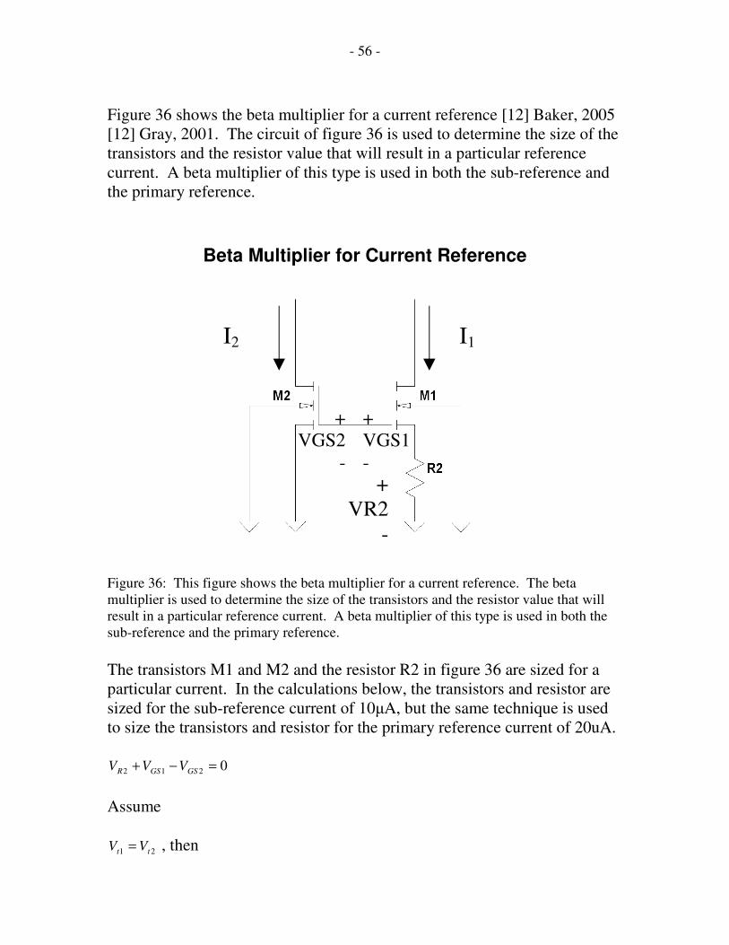
Figure 36 shows the beta multiplier for a current reference [12] Baker, 2005
[12] Gray, 2001. The circuit of figure 36 is used to determine the size of the
transistors and the resistor value that will result in a particular reference
current. A beta multiplier of this type is used in both the sub-reference and
the primary reference.
Figure 36: This figure shows the beta multiplier for a current reference. The beta
multiplier is used to determine the size of the transistors and the resistor value that will
result in a particular reference current. A beta multiplier of this type is used in both the
sub-reference and the primary reference.
The transistors M1 and M2 and the resistor R2 in figure 36 are sized for a
particular current. In the calculations below, the transistors and resistor are
sized for the sub-reference current of 10µA, but the same technique is used
to size the transistors and resistor for the primary reference current of 20uA.
0212 =−+ GSGSR VVV
Assume
21 tt VV = , then
I1 I2
+
VR2
-
+
VGS2
-
+
VGS1
-
Beta Multiplier for Current Reference

- 57 -
02 211 =−+ OVOV VVRI
022
2
2
2
1
1
11 =−+
L
WKP
I
L
WKP
IRI
If 21 II = and 1;2
1
2
2 ≥= KL
W
L
WK , then
1
2
1
2
2
IR
KP
K
K
L
W−
−=
If K=2 and I1=10uA, then R~20k.
Figure 37 is the schematic for the primary reference part of the current
reference circuit. SUB_BIASP and SUB_BIASN are voltages from the sub-
reference circuit that allow cascoding in the primary reference circuit. The
primary uses SUB_BIASP and SUB_BIASN to create the MBP and MBN
voltages that cascode the primary reference transistors. The cascodes on the
current mirrors make the primary reference current constant even though the
input voltage varies.

- 58 -
Primary Current Reference
Figure 37: This figure shows the schematic for the primary reference part of the current
reference circuit. Reference the text for details.
Figure 38 shows the reference current versus Vin. The reference current is
relatively constant even though the input voltage varies.

- 59 -
Figure 38: This figure shows the reference current versus Vin.
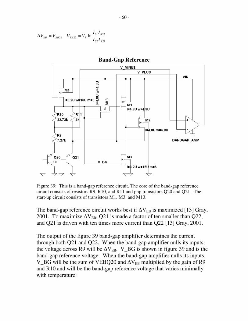
Band-gap Reference
The band-gap reference circuit provides a voltage that varies minimally with
temperature [13] Gray, 2001. The band-gap reference combines a forward
voltage VEB that decreases with temperature and the thermal voltage VT
which increases with temperature.
Figure 39 is a band-gap reference circuit. The core of the band-gap
reference circuit consists of resistors R9, R10, and R11 and pnp transistors
Q20 and Q21. The bases and collectors of the pnp transistors are both
connected to ground, so the transistors act like diodes with the cathode
grounded. As already mentioned, the band-gap reference circuit adds
together a VEB voltage and a voltage that depends on VT to get the band-gap
reference voltage that varies minimally with temperature. Q21 provides the
VEB voltage, and the difference between VEB21 and VEB20 provide ∆VEB
which includes the effect of VT with temperature [13] Gray, 2001:
Vin
Ref
eren
ce C
urr
ent
Reference Current Versus Vin
- 60 -
2122
2221
2221 lnS
S
TEBEBEBII
IIVVVV =−=∆
Band-Gap Reference
Figure 39: This is a band-gap reference circuit. The core of the band-gap reference
circuit consists of resistors R9, R10, and R11 and pnp transistors Q20 and Q21. The
start-up circuit consists of transistors M1, M3, and M13.
The band-gap reference circuit works best if ∆VEB is maximized [13] Gray,
2001. To maximize ∆VEB, Q21 is made a factor of ten smaller than Q22,
and Q21 is driven with ten times more current than Q22 [13] Gray, 2001.
The output of the figure 39 band-gap amplifier determines the current
through both Q21 and Q22. When the band-gap amplifier nulls its inputs,
the voltage across R9 will be ∆VEB. V_BG is shown in figure 39 and is the
band-gap reference voltage. When the band-gap amplifier nulls its inputs,
V_BG will be the sum of VEBQ20 and ∆VEB multiplied by the gain of R9
and R10 and will be the band-gap reference voltage that varies minimally
with temperature:

- 61 -
EBEBQ VR
RVBGV ∆
++=
9
101_ 20
The band-gap reference voltage is known to be 1.224V at room temperature.
VT=0.026V at room temperature. R11 determines the amount of current
through Q21 and R11=4k ohms. Since Q21 is driven with ten times more
current than Q22, R9+R10=40k ohms. R9 and R10 can then be determined:
119.010340
1017.0224.1
−++=
Re
R
so
39.3010 eR = and 31.99 eR = .
A band-gap reference circuit requires a start-up circuit. The start-up circuit
consists of transistors M1, M2, M3, and M13. M13 acts like a diode so M1
is turned on with less voltage at startup. M2 is sized to source about 100uA:
( )2
2
2
2
2 2
tNSGN VVKP
I
L
W
−=
( )( )
( )( )115.1
8.09.036120
26100
2
2
2
2
2
=⇒=−−−
−=
L
W
e
e
L
W
The relative sizes of M1 and M3 are determined by equating their currents.
When V_BG is at the band-gap reference voltage, M3 is on and in the linear
region and M1 is saturated. From [14] Weste, 1994:
31 MM II =
( ) ( )
−−Β−=−−−Β−
2__
2
12
2 OUT
tNNtPINtPP
VVOUTVBGVVVVBGV
( )
( )40~121
08.0
68.9
2
4.04.08.02.1
9.06.59.02.15.0
1
3
2
2
W
W
P
N ⇒==
−−
−−+=
Β
Β

- 62 -
The band-gap amplifier schematic is shown in figure 40.
Amplifier for Band-Gap Reference
Figure 40: This figure is the band-gap amplifier schematic.
The band-gap amplifier is designed according to the procedure for a two
stage amplifier in [15] Allen, 2002.
Determine CL:
The band-gap amplifier drives PMOS M4. From [12] Baker, 2005:
( )2' scaleWLCC OXOX =
( )( )( )( ) pFm
fFCOX 7.06.132.31675.1
2
2==
µ
Choose CL=2.2pF.

- 63 -
Determine CC:
fFCfFpCC CLC 5004842.210
2.2
10
2.2=⇒===
Determine I5:
Slew Rate=SR=50V/µs
( ) As
VeSRCI C µ
µ25
50155005 =−==
Determine gm1:
Choose GBW=20MHz
( ) ( ) ( )V
AeGBWCgm C
615 106310500620221 −− === ππ
Determine W1/L1 and W2/L2:
M1 and M2 are PMOS.
( )( )( ) ( )
48.310251040
1062
2
2
1
1
66
26
8
2
1
2
2
1
1 ==⇒====−−
−
L
W
L
W
IKP
g
L
W
L
W
P
m
Determine W3/L3=W4/L4:
Design M3 for an overdrive of 200mV.
( )( )
( )( )62.5
2.010120
1025
4
4
3
3
26
6
2
5
4
4
3
3 ==⇒====−
−
L
W
L
W
VovKP
I
L
W
L
W
N
Calculate the mirror pole p3:
Ideally, p3 is ten times greater than GBW.

- 64 -
( ) ( )( )( ) ( )( )
( )( )( ) ( )( )( )
( )( )
s
rad
OX
N
GS scaleCLW
IL
WKP
C
gmp
6
12
4
215
66
2
33
3
3
3
3
101541075.2
1024.4
6.11075.12.36162
102530101202
'2
2
2
3~3 =
−=
−=
−
=−
−
−
−
−−
Determine VOV1 and VOV2:
( )( )( )
Vgm
IVV D
OVOV 4.01062
105.122
1
26
6
121 ====
−
−
Determine W5/L5:
Use the band-gap reference voltage, although the actually maximum
common mode input voltage is less. The supply voltage VIN is 3V
minimum.
( )( )( )
( )( )105.2
2.19.04.031040
102522
5
5
26
6
2
11
5
5
5 =⇒=−−−
=−−−
=−
−
L
W
VVVVINKP
I
L
W
CMMAXtOVP
W5/L5=15 is normal size.
Determine gm6.
gm1=gm2.
( )( ) ( )( )
( )V
A
C
Cgmgm
C
L 4
15
126 106
10500
102.210622.222.26 −
−
−− ===
Determine gm4.
( )41024.434 −== gmgm
Determine W6/L6:
( )( )( )
949.81024.4
1066
4
64
4
6
6
4
4
6
6 =⇒===−
−
L
W
gm
gmL
W
L
W
Determine I6:

- 65 -
( )( )( )( )
A
L
WKP
gmI
N
µ7520101202
106
2
66
6
24
6
6
2
===−
−
Determine VDSSAT6:
( )( )
V
L
WKP
gmV
N
DSSAT 25.02010120
10666
4
6
6
6 ===−
−
Determine W7/L7:
4525
7515
5
6
5
5
7
7 ===I
I
L
W
L
W
Determine Av:
( )( )( ) ( )
( ) ( )( ) ( )99200
107501.021025
10610622
766)32(5
622626
46
==++
=−−
−−
λλλλ II
gmgmAV
Determine PD:
( ) ( )( ) mWPD 3.0107510253 66 =+= −−
Figure 41 shows the band-gap reference voltage versus temperature. The
voltage varies minimally with temperature.

- 66 -
Figure 41: This figure shows the band-gap reference voltage versus temperature. The
voltage varies minimally with temperature.
Shutdown Comparator
The shutdown comparator compares a dc input to a threshold voltage equal
to the band gap reference. If the input is below the threshold, the shutdown
comparator shuts off the regulator to minimize the input current to the ic.
The shutdown comparator will also prevent the switching MOSFET from
turning on. If the input is above the threshold, the regulator is on and the ic
operates. If the input to the shutdown comparator is the input voltage VIN
attenuated by a resistor divider, the shutdown comparator can sense when
the input VIN is below a certain voltage and turn off the regulator.
Figure 42 is the schematic for the shutdown comparator. The shutdown
comparator is a differential amplifier, a NAND gate, delays, and inverters
with unequal NMOS and PMOS strengths. The NAND gate, delays, and
inverters with unequal NMOS and PMOS strengths prevent an active ON
output from the shutdown comparator until there is a valid band-gap
reference voltage input V_BG.
V_
BG
Band-Gap Voltage Versus Temperature

- 67 -
Figure 42: This figure shows the schematic for the shutdown comparator. The shutdown
comparator is a differential amplifier, a NAND gate, delays, and inverters with unequal
NMOS and PMOS strengths. The NAND gate, delays, and inverters with unequal
NMOS and PMOS strengths prevent an active ON output from the shutdown comparator,
until there is a valid band-gap reference voltage input V_BG.
Figure 43 shows the output signal ON of the shutdown comparator circuit as
the input voltage VIN is ramped from 0V to 3V and back down to 1V. The
inputs to the shutdown comparator in addition to the supply voltage VIN are
not shown. One input to the shutdown comparator is the input voltage VIN
attenuated by a resistor divider. The resistor divider is chosen so the input to
the shutdown comparator will be equal to the band-gap reference voltage
when VIN is 2.8V. V_BG is the second input to the shutdown comparator.
Shutdown Comparator

- 68 -
Figure 43: This figure shows the output of the shutdown comparator circuit ON as the
input voltage VIN is ramped from 0V to 3V and back down to 1V. The inputs to the
shutdown comparator in addition to the supply voltage VIN are not shown.
Regulator
The regulator output voltage VREG is 2.9V with an input voltage VIN that
is the input voltage to the power supply circuit. VIN varies from 3V to
5.6V. The regulated 2.9V supplies input power to all the ic sub-circuits
except the band-gap reference, the current reference, the shutdown
comparator, and the sense amplifier. The first stage of the regulator is a
differential amplifier that compares the band-gap reference voltage to a
scaled-down version of the regulator output voltage. The output is scaled
down by a resistor divider. The resistors of the divider are chosen so the
input to the differential amplifier from the regulator output equals the band-
gap reference voltage when the regulator output voltage is 2.9V. The
regulator has an ON input that will turn off the regulator output when ON is
low. The ON input to the regulator comes from the shutdown comparator.
The shutdown comparator allows one of the ic’s logic inputs to turn off the
regulator and consequently shut down the power supply circuit. The
shutdown comparator also shuts down the power supply if VIN is less than
VIN
ON
Shutdown Comparator Input (VIN) and Output (ON)

- 69 -
about 2.8V. A 500fF compensation capacitor CC improves the transient
response of the regulator, and the 1uF output capacitor CL is necessary for
compensation [12] Baker, 2005. The regulator has a maximum output
current of 2mA.
Figure 44 shows the schematic of the regulator. The regulator consists of
two stages [12] Baker, 2005. The first stage is an operational trans-
conductance amplifier (OTA) [12] Baker, 2005. The second stage is a
PMOS common source amplifier [12] Baker, 2005. The OTA can pull the
gate of M7 near ground, so M7 can deliver the most current for its W/L ratio
[12] Baker, 2005. The NMOS cascodes are necessary to minimize offsets as
VIN varies from 3V to 5.6V.
Figure 44: This figure shows the schematic of the regulator.
M7 is sized so VSDSATM7=0.1V when I7=2mA.
( )( )( )
( )( )2500
1.01040
1022226
3
2
7
7
7
7 ===−
−
SDSATMP VKP
I
L
W
CL CC
RI
Regulator

- 70 -
The regulator has two poles that are necessary to consider for stability. The
first pole is determined by CGS7 and the output resistance of the OTA. From
[12] Baker, 2005:
( )2
7 ' scaleWLCC OXGS =
( )( )( )( ) pFm
fFCGS 7.286.12506.11675.1
2
27 ==µ
The output resistance of an NMOS cascode was determined experimentally
to be 22M ohms. The output resistance of a PMOS similar to M5 was
determined experimentally to be 118k ohms. The first pole that is
determined by CGS7 and the output resistance of the OTA is:
( ) ( )( ) [ ] kHzp 47107.281022//101182
1~1
1263=
−π
This is the low frequency, open-loop gain of the OTA [12] Baker, 2005:
IImIIImIOLDC RgRgA =
IImII Rg is determined experimentally to be 19.3. gmI = 150(10-6) from [12]
Baker, 2005.
( ) ( ) dBAA OLDCOLDC 6.503393.191011710150 36 =⇒== −
Since p1~47kHz, the second pole should reduce the open loop gain to about
0dB at 47kHz. Determine the frequency for the second pole:
( )Hz
A
pp
OLDC
139339
104712
3
===
Determine the minimum load capacitance CLMIN:
( )
( ) uFCLMIN 11078.0
102
9.21392
1 6
3
⇒== −
−π
Determine W3/L3:

- 71 -
( )( )( )
V
L
WKP
IV
P
SDSAT 25.0
6.1
161040
105.1222
6
6
1
1
11 ===
−
−
( )( )( )
( )( )52.3
25.09.0224.131040
10252
_
2
3
3
26
6
2
1
3
3
3 =⇒=−−−
=−−−
=−
−
L
W
VVBGVVINKP
I
L
W
SDSATtNN
W3/L3 is normal size.
W4/L4 and W5/L5 can be normal size.
Determine W18/L18:
ASGMBSATMDS VVV 4418 +≥
( )
( )
( )
( )6
6
6
18
18
6
101202.3
16
2105.122
10120
2105.128.0
−
−
−
−
=+
L
W
2
5
2.3
165.0
18
18=≤
L
W
Figure 45 shows the output voltage of the regulator VREG as the regulator
input VIN increases from 0 to 5.6V.

- 72 -
Figure 45: This figure shows the output voltage of the regulator VREG as the regulator
input VIN increases from 0 to 5.6V.
Inductor DCR Current Sensing and Sense Amplifier
This design uses the DCR of the inductor to sense the inductor current, as
discussed earlier in the Boost SMPS Basics section of this report. The inner
current loop contains a comparator that turns the switching MOSFET off
when the inductor current exceeds the current command from the error
amplifier. The inductor voltage is low-pass filtered to get the inductor DCR
voltage. The inductor DCR voltage represents the inductor current. The
sense amplifier level shifts the inductor DCR voltage and amplifies the
voltage by five. Figure 46 shows the low pass filter that derives the inductor
DCR voltage from the inductor voltage [7] Zhang, 2008.
VIN
VREG
VIN
Regulator Output Voltage Versus Vin

- 73 -
Figure 46: This figure shows the low pass filter that derives the inductor DCR voltage
from the inductor voltage [7] Zhang, 2008.
R is determined by its power dissipation. A duty cycle of 0.5 is chosen to
make the calculations easy. The nominal LED voltage of 6.75V is chosen as
the output voltage. The RMS voltage across the resistor RMSV is then:
VVVVV inoutinRMS 375.3=−==
The de-rated power for an 0805 size R is 0.0625W. Then R is:
1820625.0
375.3 2
==R
Pick R=243. According to [7] Zhang, 2008, if
DCR
LRC = , then
( )DCRsisv Lsense )()( =
)(ssensev
Inductor
+ -
)(siL
Filter for Inductor DCR Current Sensing

- 74 -
So
( )61
24309.0
622
)(−=
−== e
e
RDCR
LC
Pick C=1uF.
Figure 47 is the sense amplifier circuit that level shifts the inductor DCR
voltage and amplifies the voltage by five [16] Linear AN105, 2005.
Figure 47: This figure shows the sense amplifier circuit that level shifts the inductor
DCR voltage and amplifies the voltage by five [16] Linear AN105, 2005.
The sense amplifier is a folded cascode amplifier. The transistors for the
input differential amplifier stage are NMOS transistors so the amplifier will
operate with the inputs at the positive rail (VIN). The sense amplifier has a
push-pull output for high gain [12] Baker, 2005. The sense amplifier drives
the gate of an NMOS transistor with a 30k ohm resistor from its source to
ground. The next stage takes its signal from the 30k ohm resistor and
Inductor
DCR Sense Circuit
Error Amplifier
Sense Amplifier Level Shift and Gain

- 75 -
NMOS source. The sense amp, NMOS, 30k ohm resistor, and the 6k ohm
resistors at the sense amplifier inputs, level shift the sense amplifier inputs to
the sense amplifier output and also make the circuit have a gain of five. The
30k ohm resistor is biased with 25uA, so the DCR sensing circuit output is
always greater than 0.75V. The inductor current is limited so the level
shifted output will not exceed 1.36V. Figure 48 shows the sense amp,
NMOS, 30k ohm resistor, and the 6k ohm resistors.
Sense Amplifier Circuit
Figure 48: This figure shows the sense amp, NMOS, 30k ohm resistor, and the 6k ohm
resistors.
These are the specifications for the sense amplifier:
Vin: VVV IN 6.53 ≤≤
Vsupply: VVV SUPPLY 6.53 ≤≤
Vout: NSATTOUTNSATT VVVVVV ++≤≤++ 36.175.0
Cload: 750fF
GBW: 100MHz
Design the sense amplifier using [12] Baker, 2005, and the folded cascode
design procedure in [15] Allen, 2002. Figure 49 shows the sense amplifier.
The bias for the sense amplifier is shown separately.

- 76 -
Sense Amplifier
Figures 49: This figure shows the sense amplifier. The bias is shown separately.
Determine I3 which is the current through M3:
sVSR µ/25=
AIeSRCI L µ20618)( 33 =⇒−==
Determine I4=I5 which are the currents through M4 and M5:
354 2.1 III == to AIII µ305.1 543 ==⇒
Determine W5/L5 = W7/L7:
25.0~2
46.23
275
−=
−== OUTMAXIN
SATSDSATSD
VVVV
( ) ( )24
25.0640
)630(2222
5
5
7
7
5
5 =−
===e
e
VKP
I
L
W
L
W
SDP
Make W11/L11 and W9/L9 the same strength as W5/L5 and W7/L7.

- 77 -
89
9
11
11 ==L
W
L
W
25.0~911 SATSDSATSD VV =
Determine W1/L1=W2/L2:
( )( ) ( )( )( )
304.26206120
15700610022
3
22
3
2
1
2
2
1
1 ⇒=−−
−====
ee
ee
IKP
CGB
IKP
g
L
W
L
W
N
L
N
m
Make W3/L3 normal size:
53
3 =L
W
Determine the gain, not including the push-pull output stage according to
[12] Baker, 2005:
( ) ( ) ( )( ) 140~62.2//622157006100~//// eeeeRocaspRocasnGBCRocaspRocasngAv Lmn −==
Figure 50 shows the bias for the sense amplifier circuit.
Bias for the Sense Amplifier
Figure 50: This figure shows the bias for the sense amplifier circuit.

- 78 -
Determine the cascode bias W15/L15:
SATSDSGSD VVV 141315 +≥
( )25.025.09.0
640
26209.0
15
15
++≥
−
−+
eL
W
e
415
15 ≤L
W
Determine the cascode bias W18/L18:
SATDSSGSD VVV 10818 +≥
( )25.025.08.0
6120
265.128.0
18
18
++≥
−
−+
eL
W
e
183.018
18
18
18 =⇒≤L
W
L
W
Figure 51 shows the inductor current and the output signal from the inductor
DCR current sensing circuit.

- 79 -
Figure 51: This figure shows the inductor current and the output signal from the inductor
DCR current sensing circuit.
Oscillator
The oscillator coordinates the timing within the ic. The period of the
oscillator is 2.5 µs and is not adjustable. Figure 52 shows the oscillator
signal. The oscillator signal consists of a single pulse that occurs at the
beginning of the oscillator period. The pulse is 400ns wide, and the
amplitude of the pulse is 2.9V above ground and is the same voltage as
VREG from the regulator.
Inductor Current
Inductor DCR
Current Sensing
Signal
Inductor DCR Current Sensing Signals

- 80 -
Figure 52: This figure shows the oscillator signal. The oscillator signal consists of a
single pulse that occurs at the beginning of the oscillator period. The pulse is 400ns
wide, and the amplitude of the pulse is 2.9V above ground and is the same voltage as
VREG from the regulator.
The positive edge of the oscillator pulse initiates a switching cycle. The
oscillator initiates a switching cycle by turning the MOSFET switch off and
resetting the ramp generator. The switch will remain off for at least the
duration of the 400ns oscillator pulse. Figure 53 shows the circuit that the
oscillator uses to turn off the switch. The circuit includes a SR flip-flop, a
NOR gate, and a gate driver. The gate driver interfaces the output of the
NOR gate to the gate of the switching MOSFET. The SR flip-flop and the
NOR gate allow the switch to turn back on after the oscillator pulse if the
comparator input to the SR flip-flop allows it. The comparator is part of the
ic control circuit. One input to the NOR gate allows the ON signal from the
shutdown comparator to prevent the switch from turning on.
400ns
2.5µs
0V
2.9V=VREG
VOSC(t)
Oscillator Signal

- 81 -
Figure 53: This figure shows the circuit that the oscillator uses to turn off the switch.
The circuit includes a SR flip-flop, a NOR gate, and a gate driver.
The oscillator block diagram is shown in figure 54. The square wave
generator oscillates at 2MHz. The 2MHz square wave is then divided by
five. The divider consists of T flip-flops and the divider output is a 400kHz
square wave that is the period of the ic oscillator. The NAND gate, 400ns
delay, and the inverter create the single positive level pulse that occurs at the
beginning of the oscillator period.
Switching
MOSFET Internal to ic
From ic
control
circuit
Oscillator Circuit to Turn Off the Switch
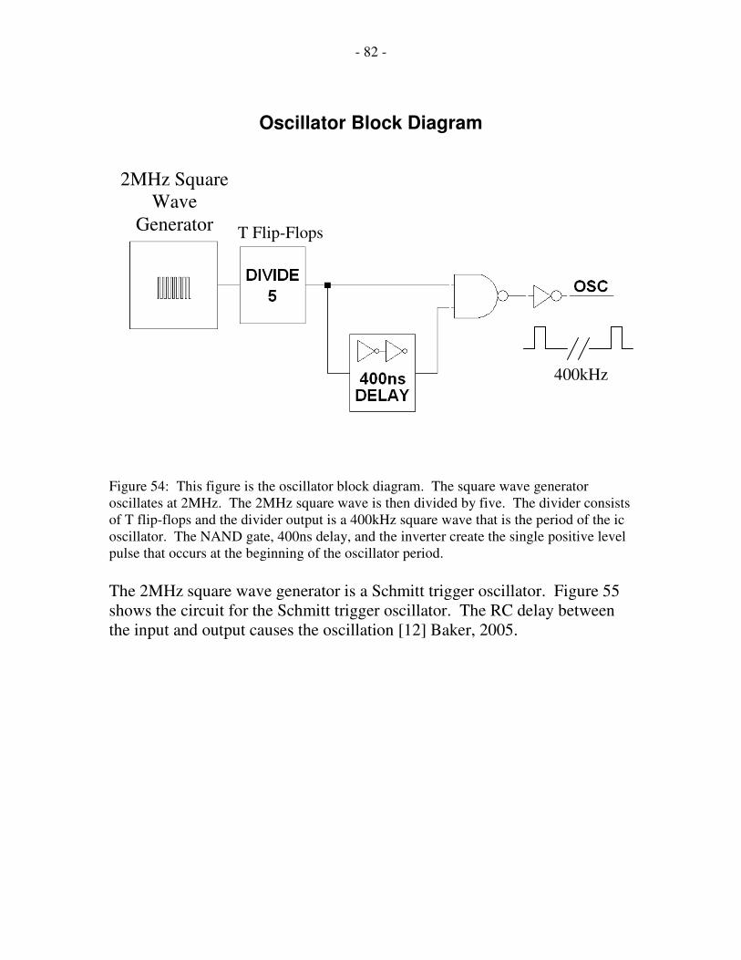
- 82 -
Figure 54: This figure is the oscillator block diagram. The square wave generator
oscillates at 2MHz. The 2MHz square wave is then divided by five. The divider consists
of T flip-flops and the divider output is a 400kHz square wave that is the period of the ic
oscillator. The NAND gate, 400ns delay, and the inverter create the single positive level
pulse that occurs at the beginning of the oscillator period.
The 2MHz square wave generator is a Schmitt trigger oscillator. Figure 55
shows the circuit for the Schmitt trigger oscillator. The RC delay between
the input and output causes the oscillation [12] Baker, 2005.
400kHz
2MHz Square
Wave
Generator T Flip-Flops
Oscillator Block Diagram

- 83 -
Figure 55: This figure shows the circuit for the Schmitt trigger oscillator. The RC delay
between the input and output causes the oscillation [12] Baker, 2005.
The Schmitt trigger in the Schmitt trigger oscillator is the Vm type [17]
Jones, 2008. The Schmitt trigger is designed for an input VH of 1.6V, a
input VL of 1.2V, and input Vm of 1.4V. VH is the input voltage that causes
the output to transition from high to low. VL is the input voltage that causes
the output to transition from low to high. Vm is the mid-point between VH
and VL. The difference between VH and VL assists noise immunity and is
called hysteresis [12] Baker, 2005.
Figure 56 shows the Vm type Schmitt trigger circuit. The Schmitt trigger is
similar to an inverter except there are extra PMOS transistors pulling the
output up and extra NMOS transistors pulling the output down [17] Jones,
2008. There is a difference between VH and VL because the NMOS is
stronger when the input is high (output is low), and the PMOS is stronger
when the input is low (output is high) [17] Jones, 2008.
2MHz
Schmitt Trigger Oscillator

- 84 -
Figure 56: This figure shows the Vm type Schmitt trigger circuit. The Schmitt trigger is
similar to an inverter except there are extra PMOS transistors pulling the output up and
extra NMOS transistors pulling the output down [17] Jones, 2008.
Ramp Generator
The ramp generator creates the ramp voltage that is added to the sensed
inductor current signal. The addition of the ramp voltage slope-compensates
the inner current loop so it is stable for all duty cycles, as discussed earlier.
The ramp voltage has a dc offset of 0.75V.
The slope compensation is 120000A/s when referenced to the inductor
current, as determined earlier. The DCR of the inductor is 0.09 ohms and
the gain of the sense amplifier circuit is five. Since the switching frequency
is 400kHz, the switching period T is 2.5µs. The amount of ramp voltage that
2.9V=VREG
Vm Type Schmitt Trigger

- 85 -
must be added to the signal for the inductor current from the sense amplifier
is:
T
V
T
s
A
V
s
AvRAMP 135.0
5.2509.0120000 ==
µ
Figure 57 shows the ramp generator circuit. The oscillator input to the ramp
generator circuit initiates each ramp generation cycle. The output of the
ramp generator circuit is added to the output of the sense amplifier circuit, to
slope-compensate the inner control loop.
Ramp Generator
Figure 57: This figure shows the ramp generator circuit. The oscillator input to the ramp
generation circuit initiates each ramp generation cycle. The output of the ramp generator
circuit is added to the output of the sense amplifier circuit, to slope-compensate the inner
control loop.
The ramp generator circuit charges up capacitor C1 with a 1µA current. The
NMOS and PMOS in the ramp generator circuit are cascoded so the current
remain constant as C1 charges. The OSC signal resets the ramp generator at
the beginning of each switching cycle.
Figure 58 shows the output of the ramp generator circuit.

- 86 -
Figure 58: This figure shows the output of the ramp generator circuit.
Summer
Figure 59 shows the summer circuit. The summer circuit adds the slope
compensation voltage from the ramp generator to the voltage that represents
the inductor current from the sense amplifier. The circuit consists of three
amplifiers. Two of the amplifiers are configured as unity gain buffers. One
amplifier buffers the signal from the ramp generator and the other amplifier
buffers the inductor current signal from the sense amplifier. The last
amplifier is a unity gain summer amplifier with inputs from the two buffers.
Ramp Generator
Output Voltage
Ramp Generator Output

- 87 -
Figure 59: This figure shows the summer circuit. The summer circuit adds the slope
compensation voltage from the ramp generator to the voltage that represents the inductor
current from the sense amp.
All the amplifiers in the summer circuit are folded cascode amplifiers [12]
Baker, 2005. The transistors for the input differential amplifier stage are
PMOS transistors. The amplifiers have push-pull outputs for high gain [12]
Baker, 2005.
These are the specifications:
Vin: VVV IN 4.175.0 ≤≤
Vsupply: 2.9V=VREG
Vout: VVV OUT 3.275.0 ≤≤
Cload: 750fF
GBW: 100MHz
The summer circuit amplifiers are designed using [12] Baker, 2005, and the
folded cascode design procedure in [15] Allen, 2002. Figure 60 shows the
circuit for the summer circuit amplifiers. The bias for the amplifiers is
shown separately.
From Ramp
Generator
0.75V-0.89V
Inductor
Current Signal
0.75V-1.29V
To Comparator
1.5V-2.18V
Summer Circuit
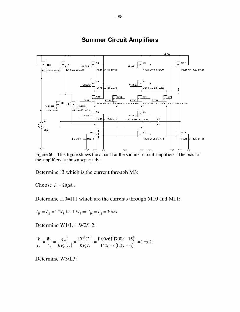
- 88 -
Figure 60: This figure shows the circuit for the summer circuit amplifiers. The bias for
the amplifiers is shown separately.
Determine I3 which is the current through M3:
Choose AI µ203 = .
Determine I10=I11 which are the currents through M10 and M11:
31110 2.1 III == to AIII µ305.1 11103 ==⇒
Determine W1/L1=W2/L2:
( )( ) ( )
( )( )21
620640
15700610022
3
22
3
2
1
2
2
1
1 ⇒=−−
−====
ee
ee
IKP
CGB
IKP
g
L
W
L
W
P
L
P
m
Determine W3/L3:
Summer Circuit Amplifiers

- 89 -
( )( ) ( )
( )
HUGEe
VVVVREGKP
I
L
W
tPSDSATCMMAXP
=
−−−
=−−−
=
−
−−
2
6
66
2
3
3
3
3
9.01040
10204.19.21040
)620(22
1003
3 =⇒L
W
Figure 61 shows the bias for the summer circuit amplifiers.
Figure 61: This figure shows the bias for the summer circuit amplifiers.
The cascode bias stacks for FCSN and FCSP must fit between ground and
the 2.9V VREG.
FCSN: 2(VGS)+2VDS(SAT)=2VtN+4VDS(SAT)
( )
325.04
)8.029.2)( =
−=MAXSATDSV
Bias for the Summer Circuit Amplifiers

- 90 -
( )
( )4041
10120
2103011.0
6
6
=⇒=⇒=−
−
N
N
N
N
N
N L
W
L
W
L
W
FCSP: 2(VSG)+2VSD(SAT)=2VtP+4VSD(SAT)
( )
275.04
)9.029.2)( =
−=MAXSATSDV
( )
( )120123
1040
2103011.0
6
6
=⇒=⇒=−
−
P
P
P
P
P
P L
W
L
W
L
W
Determine the cascode bias W15/L15:
SATSDSGSD VVV 141315 +≥
( )11.011.09.0
640
26209.0
15
15
++≥
−
−+
eL
W
e
2015
15 ≤L
W
Determine the cascode bias W18/L18:
SATDSSGSD VVV 10818 +≥
( )11.011.08.0
6120
265.128.0
18
18
++≥
−
−+
eL
W
e
618
18 ≤L
W
Figure 62 shows the summer circuit input and output signals. One input
signal is the slope compensation voltage from the ramp generator and the
other input signal is the voltage that represents the inductor current from the
sense amp. The output signal of the summer circuit is the addition of the
two input signals.

- 91 -
Figure 62: This figure shows the summer circuit input and output signals. One input
signal is the slope compensation voltage from the ramp generator and the other input
signal is the voltage that represents the inductor current from the sense amp. The output
signal of the summer circuit is the addition of the two input signals.
Error Amplifier Current Reference
The error amplifier current reference provides a current for comparison to
the LED current. It can provide a reference for full brightness and a
reference for a dimmed LED, based on a logic input to the ic. Figure 63
shows the schematic for the error amplifier current reference. There is a
25µA current source. When the BRIGHT signal is high, 15µA is subtracted
from the 25µA current source, and the remaining 10µA is sourced as the
error amplifier current reference. When the BRIGHT signal is low, 20µA is
subtracted from the 25µA current source, and the remaining 5µA is sourced
as the error amplifier current reference.
Slope
Compensation
Voltage
Inductor Current Signal
Summer Output Signal
Summer Circuit Input and Output Signals

- 92 -
Figure 63: This figure shows the schematic for the error amplifier current reference.
Figure 64 shows the current that is sourced from the error amplifier current
reference circuit.
Error Amplifier Current Reference

- 93 -
Figure 64: This figure shows the current that is sourced from the error amplifier current
reference circuit.
Error Amplifier
The error amplifier is a trans-conductance amplifier with inputs that
compare the error amplifier current reference to the LED current. The error
amplifier and the resistor capacitor (RC) network at the output of the error
amplifier compensate the feedback loop and are shown in figure 65. The RC
makes a compensation zero. The output resistance rO of the trans-
conductance amplifier and the C make a compensation pole. The error
amplifier trans-conductance gm and output resistance rO determine the dc
gain of the error amplifier. The error amplifier also has a gain-bandwidth
product (GBW) that adds a pole to the compensation.
5µA
Current Sourced from the Error Amplifier
Current Reference Circuit
10µA
BRIGHT
Error Amplifier Current Reference Signals

- 94 -
Figure 65: The error amplifier and the resistor capacitor (RC) network at the output of
the error amplifier compensate the feedback loop.
These are the specifications:
Vin: VVV IN 1.00 ≤≤
Vsupply: 2.9V=VREG
Vout: VVV OUT 3.275.0 ≤≤
Iout: 50uA
Rout: 2M ohm
GBW: 50MHz (optional)
gmOTA: 300µS
Figure 66 shows the transistor level design of the error amplifier according
to [12] Baker, 2005. The circuit is an operational trans-conductance
amplifier (OTA) with PMOS transistors for the differential amplifier input
stage [12] Baker, 2005. The amplifier NMOS and PMOS are cascoded to
increase the output resistance rO [12] Baker, 2005. The output resistance for
the OTA in figure 66 is about 2M ohm. rO for the output stage NMOS and
PMOS were determined by simulation.
Error
Amp
Ref.
LED
Curr.
rO
gm
GBW
Error Amplifier To
Comparator
Error Amplifier Circuit
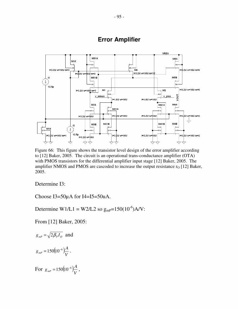
- 95 -
Figure 66: This figure shows the transistor level design of the error amplifier according
to [12] Baker, 2005. The circuit is an operational trans-conductance amplifier (OTA)
with PMOS transistors for the differential amplifier input stage [12] Baker, 2005. The
amplifier NMOS and PMOS are cascoded to increase the output resistance rO [12] Baker,
2005.
Determine I3:
Choose I3=50µA for I4=I5=50uA.
Determine W1/L1 = W2/L2 so gmP=150(10-6
)A/V:
From [12] Baker, 2005:
DPmP Ig β2= and
( )V
AgmP
610150
−= .
For ( )V
AgmP
610150
−= ,
Error Amplifier

- 96 -
( )( )( )( ) ( )
1025.11102510402
10150
2
2
1
1
66
26
2
2
1
1 ==⇒===−−
−
L
W
L
W
L
W
L
W
The common mode range for Vminus and Vplus extends to ground.
Determine VDS(SAT)M41=VDS(SAT)M31:
VVVtPVtNV MSATDSMSATDS 1.00 41)(41)( =⇒=−+
Determine W41/L41=W31/L31:
( )( )
( )( )( )5.10
1.0101202
102526
6
2
41)(
3
31
31
41
41 ====−
−
MSATDSN VKP
I
L
W
L
W
Choose W41/L41=W31/L31=5.
W6/L6 is not critical for common mode range, so choose W6/L6=60.
Determine K for gmOTA=300µS:
This small signal analysis is from [12] Baker, 2005:
21 ββ = , and 4131 ββ = .
( ) d
mP
dd iusvplusvg
ii =−==− min__2
4131 .
If 331414 ββββ KKK === and 551 ββ =K ,
then
314154 dddd KiKiii −==−= .
If 1/CLs >> rO4//rO5,
then

- 97 -
( )54 //min__
OOmPV rrKgusVplusv
voutA =
−=
If 1/CLs << rO4//rO5,
dddout Kiiii 254 =−=
and
mp
out
mOTA Kgusvplusv
ig =
−=
min__.
( )( )
210150
103006
6
===−
−
mp
mOTA
g
gK
rO4//rO5=2M ohm according to simulation.
Figure 67 is a Bode plot for the error amplifier. The Bode plot shows that
the error amplifier gain is 432 V/V. The desired gain is 600V/V. The gain
and phase roll off at decreasing frequencies due to the test bench.
V
VAV 43210 20
7.52
== .
( ) ( ) 60010300102 66
)( === −mOTAODESIREDV grA .

- 98 -
Figure 67: This figure is a Bode plot for the error amplifier. The Bode plot shows that
the error amplifier gain is 432 V/V. The desired gain is 600V/V. The gain and phase roll
off at decreasing frequencies due to the test bench.
Comparator
The comparator compares the output of the error amplifier to the output of
the summer to determine when to turn the switch off. If the comparator does
not turn the switch off, the oscillator pulse will turn the switch off for 400ns
and then turn it back on.
These are the specifications:
VIN_CM: VVV CMIN 3.25.1 _ ≤≤
Vsupply: 2.9V=VREG
Vout: VVOUT 8.0< and OUTVV <0.2
Propagation delay targets: trO1=trOUT=tfO1=tfOUT=15ns
Cout: 1pF
V
VAV 432
20
7.5210 ==
Error Amplifier Bode Plot

- 99 -
Figure 68 is the schematic for the comparator. The comparator is a two-
stage operational amplifier with NMOS transistor inputs to the differential
amplifier first stage [15] Allen, 2002. There is no compensation capacitor
[15] Allen, 2002. The configuration with NMOS input transistors drives the
output high fast [15] Allen, 2002.
Figure 68: This figure shows the schematic for the comparator. The comparator is a
two-stage operational amplifier with NMOS transistor inputs to the differential amplifier
first stage [15] Allen, 2002. There is no compensation capacitor [15] Allen, 2002. The
configuration with NMOS input transistors drives the output high fast [15] Allen, 2002.
Determine W1/L1=W2/L2 and W5/L5. The minimum common mode input
voltage is 1.5V, so make VOV1=VOV2=0.4V and VOV5=0.3V.
( )( )( )( )
124.104.010120
210100
2
2
1
1
26
6
2
2
1
1 ==⇒===−
−
L
W
L
W
L
W
L
W
Vout
VO1
Comparator

- 100 -
( )( )( )( )
40373.010120
210200
5
5
26
6
5
5 =⇒==−
−
L
W
L
W
Make the currents large and the parasitic capacitance of M6 small to
minimize propagation delays. First assume that v_plus is just lower than
v_minus, so
VREGVVVREG OSATSD <<− 1)(4 and VVout 0~ [15] Allen, 2002.
Determine I5 so the falling delay of the first stage tf1 is approximately 15ns,
according to the target specification. From [15] Allen, 2002:
5
1
1I
VCt O
If
∆=∆
Calculate ∆VO1 from the trip point of the second stage [15] Allen, 2002.
Assume I6=I7=100µA and W6/L6=W7/L7=20 for now. First determine
VSG6 when the output stage is at the trip point:
( ) AVVL
WKPtPSG
P µ1002
2
6
6
6 =−
( ) ( ) VVAV SGSG 4.11009.0202
10406
2
6
6
=⇒=−−
µ
Now determine the trip point of the second stage [15] Allen, 2002:
VTRIP2=2.9-1.4=1.5V.
Now calculate ∆VO1 [15] Allen, 2002:
∆VO1~2.9-1.5=1.4V
CI is the sum of the capacitances at the vO1 node, but assume CGS6 is
dominant. Calculate CGS6 according to [15] Baker, 2005:
( )( )( )( ) fFm
fFCGS 6126.142.31675.1
3
2 2
26 ==µ

- 101 -
Now determine I5 so the falling delay of the first stage tf1 is approximately
15ns, according to the target specification [15] Allen, 2002:
( )( ) A
t
VCI
f
OI µ57
1015
4.110612
9
15
1
15 ==
∆
∆=
−
−
Choose I5=200µA.
Determine the rising delay of the second stage trOUT [15] Allen, 2002.
Assume the comparator drives a unit inverter with CGS = 0.93pF. Determine
I6. Assume VO1 will be half way between the trip point of the second stage
and VO1’s final destination [15] Allen, 2002. Assume I7=100µA at the trip
point and VG1=1.9V. Determine VO1’s final destination:
( )( )( )
VVVVV GSGOG 73.01210120
1010028.09.1~
6
6
2116 =−−=−=−
−
Now assume
VVG 27.173.02
73.08.16 =+
−= .
Determine I6:
( ) ( ) AI µ2019.029.19.2202
1040 26
6 =−−=−
Now determine the rising delay of the second stage trOUT:
( ) nsAA
trOUT 14100201
2
9.2
10933 15 =−
=∆ −
µµ
Determine the rising delay of the first stage trO1 [15] Allen, 2002. VO1 will
start around VS1~VS2 and rise to the trip point of the second stage.
VS1~VS2~1.9-0.8=1.1V

- 102 -
( )( )
nstr 1.210200
1.18.110612
6
15
1 =−
=∆−
−
Determine the falling delay of the second stage tfOUT [15] Allen, 2002.
Assume that Vout=2.9V before it falls, and M6 is off.
( )( )
nst fOUT 5.1310100
2
9.2
109336
15 ==∆−
−
Determine W3/L3=W4/L4=W6/L6:
1.4V.0.82.32.9 V V-VREGV tNECOMMON_MODSG3 =+==+= +
( )( )( )( )
209.04.11040
1020026
6
6
6
4
4
3
3 =−
===−
−
L
W
L
W
L
W
Determine W7/L7:
( )( )( )( )
206.28.010120
10200
7
7
26
6
7
7 =⇒==−
−
L
W
L
W
Figure 69 shows operation of the comparator.

- 103 -
Figure 69: This figure shows operation of the comparator.
Soft-start Current Reference
Figure 70 shows the soft-start current reference. The soft-start current
reference charges the soft-start capacitor according to the shutdown
comparator. The soft-start capacitor clamps the output of the error amplifier
to prevent over-shoot of the inductor current during start-up. Without soft-
start, the inductor current may overshoot during start-up when VIN is first
applied to the circuit, or the logic input to the ic for shutdown changes from
low to high.
Comparator
Output
Comparator
Minus Input
Comparator
Plus Input
Comparator Operation

- 104 -
Figure 70: This figure shows the soft-start current reference. The soft-start current
reference charges the soft-start capacitor according to the shutdown comparator. The
soft-start capacitor clamps the output of the error amplifier to prevent over-shoot of the
inductor current during start-up.
Gate Driver
The gate driver interfaces the output of the NOR gate to the gate of the
switching MOSFET. Figure 71 shows the gate driver circuit. The gate
driver is a series of inverters with increasing W/L ratios.
Soft-Start Current Reference
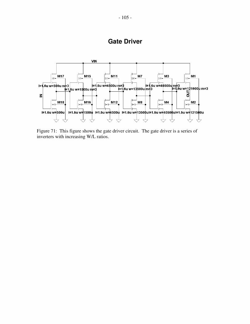
- 105 -
Figure 71: This figure shows the gate driver circuit. The gate driver is a series of
inverters with increasing W/L ratios.
Gate Driver

- 106 -
Summary and Conclusion
This project designed a boost SMPS current regulator controller ic. The
control system was designed first so the design at the transistor level that
followed would be stable without re-design. The control-to-output transfer
function used to design the control system was derived for a boost SMPS
with CPM-with-slope-compensation control. There was no direct way to
make sure the derived transfer function was correct. The identical control-
to-output transfer function for a boost was not derived in the literature cited
[4] Erickson, 1997, [10] Middlebrook, 1985, and [6] Bruzos, 1989. In the
literature, the transfer functions for a buck-boost were derived instead. Also,
there appeared to be at least one typo related to the boost transfer function in
[6] Bruzos, 1989. For those reasons, the transfer functions for voltage mode
control and simple CPM control were derived in this report prior to the
derivation of the CPM-with-slope-compensation control transfer function.
The transfer functions for voltage mode control and simple CPM control
were relatively easy to verify from the literature. The transfer function for
the more complicated and difficult to verify CPM-with-slope-compensation
control was derived as an extension of the simpler derivations that were
known to be correct.
This project used the CPM-with-slope-compensation control transfer
function to design the control system, but the simple CPM control transfer
function is probably adequate for most designs. The CPM-with-slope-
compensation control transfer function shows that there are two poles
instead of one, but the second pole is at such a high frequency it can be
neglected for practical designs. The high frequency pole is due to the slope
compensation.
The transfer function for CPM-with-slope-compensation control was also
checked by comparing its Bode plot to the Bode plot from a SwitcherCad
(SPICE) simulation. The Bode plots were similar enough that the derived
transfer function could be used to design the control system. The Bode plots
were most similar at the gain crossover frequency, but were not exactly the
same in other areas. The discrepancy would be a good area for further
study.
Several approaches to find the CPM-with-slope-compensation control
transfer function were investigated, but finally the approach of [10]
Middlebrook, 1985, and [6] Bruzos, 1989 was chosen over that of [4]

- 107 -
Erickson, 1997. These approaches are all approximations, because they do
not include the effect of output capacitor ESR when the average switch
model is determined.
All the transistor level designs were done on paper before the schematics
were entered. This approach made it easy to correct problems found during
simulations and probably shortened the design cycle. Each sub-circuit was
tested by itself before it was incorporated into the system. The basis of most
of the circuit designs were found in textbooks or the course work.

- 108 -
Appendix A1: Basic Driver Design
First determine the maximum duty cycle. There are many sources that show
how to determine duty cycle for boost converters based on the operating
conditions. Two sources are [4] Erickson, 1997 and [3] Mohan 2007.
63.016.8
316.8max =
−=D
Determine L. Assume maxi∆ occurs at 5.0=D . This L sets the ripple current
to just over 100% of the average inductor current at D=0.5 and maximum
VLED:
( )( )
HLee
L µ2254.33.03400
5.016.8=⇒−==
Determine Cout. This Cout will result in approximately 100mV of output
voltage ripple at Dmax:
( )
( )FCoute
eCout µ7.4673.4
1.03400
63.03.0=⇒−==
Determine Cin. This Cin will result in approximately 100mV of variation on
VCin:
( )
( )A
eei 464.0
6223400
5.016.8=
−=∆
( ) Ce
Q µ288.03400
5.046.0
2
1==
FCinee
Cin µ7.4688.21.0
6288.0=⇒−=
−=

- 109 -
Appendix A2: Determine Average Equations
The first step to find the control-to-output transfer function for any of the
SMPS models discussed in this report is to determine the average equations.
First the voltage and current equations for the inductor and capacitor are
determined. Also, the input voltage vg(t) and the output voltage v(t) are
replaced with their low frequency averaged values according to the small
ripple approximation [4] Erickson, 1997. Starting with figure 9, the driver is
divided into two circuits: one that represents the driver when the switch is
on, and one that represents the driver when the switch is off. Figure 10 is
the circuit for when the switch is on, and figure 11 is the circuit for when the
switch is off.
These are the voltage and current equations for the inductor and capacitor
for when the switch is on, replacing v(t) and vg(t) with their low frequency
averaged values.
TL tvgdt
tdiLtv )(
)()( ==
TC tvRdt
tdvCti )(
1)()( −==
These are the equations for when the switch is off:
TTL tvtvgdt
tdiLtv )()(
)()( −==
TTC tvR
tidt
tdvCti )(
1)(
)()( −==
Average the inductor waveforms:
TTT
Tt
tLTL tvtdtvgtdtvgtddv
Ttv )()(')()(')()(~)(
1)( −+= ∫
+
ττ
TT tvtdtvg )()(')(~ −
But

- 110 -
T
TLtvL
dt
tidL )(
)(=
So
TT
TLtvtdtvg
dt
tidL )()(')(
)(−=
Average the capacitor waveforms:
TTT
Tt
tCTC
R
tvtdtitd
R
tvtddi
Tti
)()(')()('
)()(~)(
1)( −+
−= ∫
+
ττ
TTR
tvtitd
)()()('~ −
So
TT
T
R
tvtitd
dt
tvdC
)()()('
)(−=
Average input current:
TT titig )()( =

- 111 -
Appendix A3: Perturb and Linearize Average Equations
Next the equations for the boost converter averaged equations are perturbed
and linearized. The input and output values are assumed to be equal to some
quiescent value plus a superimposed small ac variation [4] Erickson, 1997:
Inputs:
)()(^
tgvVgtvg T +=
)()(^
tdDtd +=
So
)(')))((1())(1()('^^
tdDtdDtdtd −=+−=−=
Outputs:
)()(^
tiIti T +=
)()(^
tvVtv T +=
)()(^
tgiIgtig T +=
The above “perturbed” representations for the inputs and outputs are
substituted into the averaged inductor, capacitor, and current waveform
equations. The equations are then multiplied out. Then the 1st order terms
are equated, and the DC and 2nd
order terms are dropped [4] Erickson, 1997.
Inductor:
+
−−+=
+
)()(')(
)(^^^
^
tvVtdDtgvVgdt
tiId
L
)()(')()( ^^^
^
tdVtvDtgvdt
tidL +−=⇒

- 112 -
Capacitor
+−
+
−=
+
)(1
)()('
)(^^^
^
tvVR
tiItdDdt
tvVd
C
)(1
)()(')( ^^^
^
tvR
ItdtiDdt
tvdC −−=⇒
Input Current
)()(^^
tiItgiIg +=+
)()(^^
titgi =⇒
When the above derivatives are set to 0, the familiar dc relations for a boost
converter result:
'D
VgV =
'IDR
V=
IIg =
= 0
dt
dIL
= 0
dt
dVC

- 113 -
Appendix A4: Voltage Mode Boost Converter Control-to-Output
Transfer Function
According to superposition, the small signal output voltage )(^
sv is a function
of the small signal control )(^
sd and small signal input voltage )(^
sgv [4]
Erickson, 1997:
)()()()()(^^^
svsGsdsGsv ggvdv +=
And so two transfer functions are defined where
0)(^)(
)()(
^
^
=
=
sgvsd
svsGvd
And
0)(^)(
)()(
^
^
=
=
sdsgv
svsGvg
To find the transfer functions, first take the Laplace of the inductor,
capacitor, and input current average equations with the zero initial
conditions [4] Erickson, 1997:
)()(')()(^^^^
sdVsvDsgvsisL +−=
)()(
)(')(^
^^^
sdIR
svsiDsvsC −−=
)()(^^
sisgi =
Solve for )(^
si in the inductor voltage equation, and then substitute for )(^
si in
the capacitor current equation.

- 114 -
+−= )()(')(
1)(
^^^^
sdVsvDsgvsL
si
)()(
)()(')(1
')(^
^^^^^
sdIR
svsdVsvDsgv
sLDsvsC −−
+−=
Now solve for )(^
sv in terms of )(^
sgv and )(^
sd .
( ) ( ) ( ) ( )
)('
''1
'1
)(
''1
'
1
)(^
2
22
^
2
22
^
sdD
V
sD
LCs
DR
L
sVD
IL
sgv
sD
LCs
DR
LDsv
++
−
+
++
=
So the control-to-output transfer function of the voltage mode boost
converter in CCM is
( ) ( )'
''1
'1
0)(^)(
)()(
2
22
^
^
D
V
sD
LCs
DR
L
sVD
IL
sgvsd
svsGvd
++
−
=
=
=

- 115 -
Appendix A5: Simple CPM Boost Converter Control-to-Output
Transfer Function
The simplified model of a CPM boost converter makes the assumption that
the inductor current is the same as the reference from the outer control loop,
which is called the control current. The Laplace of the inductor, capacitor,
and input current average equations with the zero initial conditions [4]
Erickson, 1997 are again used, to find the control-to-output transfer function
of the boost converter in CCM using the simplified CPM model. Now the
assumption is made that the inductor current is identical to the control
current [4] Erickson, 1997:
)()(^^
scisi L =
Now determine the relationship between )(^
sci and )(^
sd using the Laplace
equations and the inductor current to control current relation. This is the
Laplace equation for the inductor voltage from before, solved for )(^
sd :
+−≈ )(')()(
1)(
^^^^
svDsgvscisLV
sd
Use )(^
sd from above in the Laplace equation for the capacitor current, and
also use the inductor current to control current relation:
+−−−≈ )(')()(
)()(')(
^^^^
^^
svDsgvscisLV
I
R
svsciDsvsC
Use the dc relations for a boost converter from above, and multiply-
out )(^
svsC .
'
1)(
11)(
'
1')()(
^^^^
RDsgv
RRsvsL
RDDsicsvsC +
+−
−≈
Rearrange to get the equation that describes the CPM boost equivalent
circuit using the simplified model:

- 116 -
'
1)(
1)(
1)(
'1')()(
^^^
2
^^
RDsgv
Rsv
Rsv
RD
sLDsicsvsC +−−
−≈

- 117 -
Appendix A6: CPM with Slope Compensation Control-to-Output
Transfer Function
The model for the CPM with slope compensation boost converter is similar
to the simple CPM model, except )(^
si L is no longer equal to )(^
sci . Instead,
there is an equation called the control law for )(^
sd that includes the effect of
input voltage )(^
svg , control current )(^
sic , output voltage )(^
sv , steady state
duty cycle D, switching period T, inductance L, and slope compensation Ma
[4] Erickson, 1997. From [4] Erickson, 1997 the control law equation for
the CPM boost converter is:
( )
−
−−−= )(
2
')(
2
12)()(
1)(
^2^^^
tvL
TDtgv
L
TDtitci
MaTtd L
One way to find the control-to-output transfer function for the CPM boost
converter is to first make a y-parameter model using the Laplace inductor,
capacitor, and input current average equations that are already derived, and
the control law [10] Middlebrook, 1985 and [6] Bruzos, 1989. The y-
parameter model has an input port and an output port, but only the output
port is necessary to find the control-to-output transfer function [18]
Middlebrook, 1989. Figure A51 is the y-parameter model output port:

- 118 -
Figure A51: This is the y-parameter model output port and is all that is necessary to find
the control-to-output transfer function for the CPM boost converter.
The control voltage )(^
spv is the product of scaling resistor Rf and the control
current )(^
sci :
)()(^^
sciRfspv =
From figure A51, y2c and y22 are necessary to find the control-to-output
transfer function. First find y2c(s).
)(
)(^
^
0^^
)(2
spv
soi
vgv
scy
==
=
Using the Laplace of the control law, and the relation between )(^
spv and
)(^
sci , and the equation for y2c(s) from above:
T
si
RfT
spvMasd
)()()(
^^^
−=

- 119 -
Use the Laplace inductor voltage equation, and the equation for )(^
td from
above, and the equation for y2c(s):
−=
MaT
si
MaRfT
spv
L
Vsis
)()()(
^^^
Solve for )(^
si :
LMaT
Vs
MaRfT
spv
L
V
si
+
=
)(
)(
^
^
From figure 12, the Laplace of the equation for the output current with zero
initial conditions is:
)()(')(^^^
sdIsiDsoi −=
Substitute the equation for )(^
td :
−−=
MaT
si
MaRfT
spvIsiDsoi
)()()(')(
^^^^
Solve for )(^
si :
MaT
ID
MaRfT
spIvsoi
si
+
+
=
'
)()(
)(
^^
^
Use the equations from above to eliminate )(^
si :
)()(^^
sisi =

- 120 -
MaT
ID
MaRfT
spIvsoi
LMaT
Vs
MaRfT
spv
L
V
+
+
=
+ '
)()(
)(^
^^
Solve for y2c(s):
( )ILsVDTRfL
TL
VMas
vgv
scy
spv
soi−
+
=
==
= '11
^
^
0^^
)(2
)(
)(
Now find y22(s).
)(
)(^
^
0^^
)(22
sv
soi
vpgv
sy
==
=
Using the control law, and the equation for y22(s) from above:
)(2
')()(
^2^
^
svL
D
T
siMasd −−=
Use the Laplace of the inductor voltage equation, the equation for )(^
td from
above, and the equation for y22(s):
−−+
−= )(
2
')()(')(
^2^^
^
svLMa
D
TMa
si
L
V
L
svDsis
Solve for )(^
si :

- 121 -
LTMa
Vs
LMa
D
L
V
L
Dsv
si
+
−
−
=2
'')(
)(
2^
^
Use the Laplace of the equation for the output current, the equation for )(^
td
from above, and the equation for y22(s):
−−−= )(
2
')()(')(
^2^
^^
svLMa
D
TMa
siIsiDsoi
Solve for )(^
si :
TMa
ID
svLMa
DIsoi
si
+
−
=
'
)(2
')(
)(
^2^
^
Use the equations from above to eliminate )(^
si :
TMa
ID
svLMa
DIsoi
LTMa
Vs
Ma
D
L
V
L
Dsv
+
−=
+
−
−
'
)(2
')(
2
'')(
^2^2
2
^
Solve for y22(s):
( )
TL
VMas
TVDLIDTMaLDTL
sL
ID
vpgv
sy
sv
soi
+
−−−+
=
==
=
33
2
2
'2'2'2
1
2
'
^
^
0^^
)(22
)(
)(
Now y2c and y22 and figure A51 are used to find the control-to-output
transfer function:

- 122 -
RCsy
cRfy
usic
sv
122
2
0)(
)(
++−
==
Substitute in y2c(s):
( )
RCsy
RfILsVDTRfL
TL
VMas
122
1'
11
++−
−
+
=
Simplify and substitute in y22. Note the polarity of y22 compared to io:
( )( )
RCs
TL
VMas
TVDLIDTMaLDTL
sL
IDILsVD
TL
TL
VMas
1'2'2'
2
1
2
'
1'
11
33
2
2
++
+
−−−−−
−
+
=
Continue to simplify and collect terms. These relationships are useful:
2'' RD
Vg
RD
VI ==
'11 D
U
D
U
D
VgVVgVVD
V
VgVD =
−=
−
−=⇒−=⇒
−=
This is the control-to-output transfer function for the CPM boost converter in
CCM:
CL
TVgD
RLC
Vg
LC
MaTD
RCLD
Vgs
RC
MaT
LD
Vg
LCR
TVgMaTs
LC
Vgs
CRD
Vg
sic
sv
u2
232
2
2
''
''2
'
)(
)(
0 ++++
++−+
+−
==

- 123 -
References
1. Tsao, Jeffrey, “Roadmap projects significant LED penetration of
lighting market by 2010”, Laser Focus World (Sandia National
Laboratories), May, 2003.
2. Osram Opto Semiconductors, Gmbh Application Note, “Diamond
Dragon – The Brightest Star of the Dragon Family”, October,
2008.
3. Mohan, N., First Course on Power Electronics, 2007 Edition,
MNPERE, Minneapolis, 2007.
4. Erickson, Robert W., Fundamentals of Power Electronics, Kluwer
Academic Publishers, Norwell, Massachusetts, 1997.
5. Brown, Marty, Power Supply Cookbook, Butterworth-Heinemann,
Newton, Massachusetts, 1994.
6. Bruzos, C. A., “Modeling and Control Approaches for Multi-
Output Switched Converters,” Master’s thesis EECS Dept., M.I.T.,
1989.
7. Zhang, Henry, Internal Linear Technology Tutorial Presentation,
2008
8. Kuo, B. C., Automatic Control Systems, 6th Edition, Prentice Hall,
Englewood Cliffs, New Jersey, 1991.
9. Erickson, Robert W. and Maksimovic, Dragan, “A Primer on
Simulation, Modeling, and Design of the Control Loops of
Switching Regulators,” IEEE APEC Tutorial Seminar, 2003.
10. Middlebrook, R. D., Topics in Multiple-Loop Regulators and
Current-Mode Programming, IEEE PESC, 1985 Record, pp.716-
732.
11. Seago, John, Linear Technology Application Note 76, “OPTI-
LOOP Architecture Reduces Output Capacitance and Improves
Transient Response”, 1999.
12. Baker, R. Jacob, CMOS Circuit Design, Layout, and Simulation,
2nd
Edition, Wiley-IEEE Press, Piscataway, NJ, 2005.
13. Gray, Paul R., Analysis and Design of Analog Integrated Circuits,
4th
Edition, John Wiley and Sons, New York, 2001.
14. Weste, Neil H. E. and Eshraghian, Kamran, Principles of CMOS
VLSI Design: A Systems Perspective, 2nd
Edition, Addison-
Wesley Publishing Company, Reading, MA, 1994.
15. Allen, Phillip E., CMOS Analog Circuit Design, 2nd
Edition,
Oxford University Press, New York, NY, 2002.

- 124 -
16. Linear Technology Application Note 105, “Current Sense Circuit
Collection”, 2005.
17. Jones, Morris, EE227 Lecture Notes, San Jose State University,
2008
18. Middlebrook, R. D., “Modeling current programmed buck and
boost regulators,” IEEE Trans. Power Electronics, 36-52, January
1989.


