
1
Regulating Solid State Diffusion in Semiconductor Processing
Edmund G. SeebauerDepartment of Chemical Engineering
University of Illinois at Urbana-Champaign
Support: NSF, DOE, Chartered Semiconductor
2
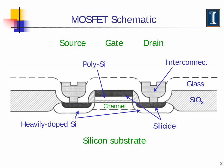
MOSFET Schematic
Source Gate Drain
Silicon substrate
Interconnect
Glass
SiO2Channel
Silicide
Poly-Si
Heavily-doped Si
3
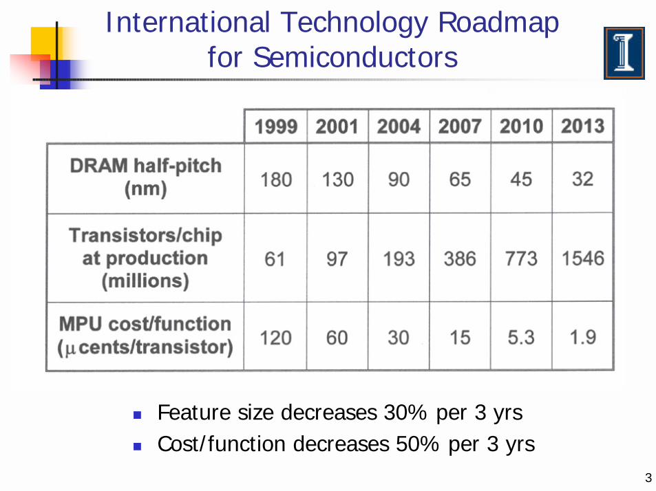
International Technology Roadmap for Semiconductors
! Feature size decreases 30% per 3 yrs! Cost/function decreases 50% per 3 yrs
4
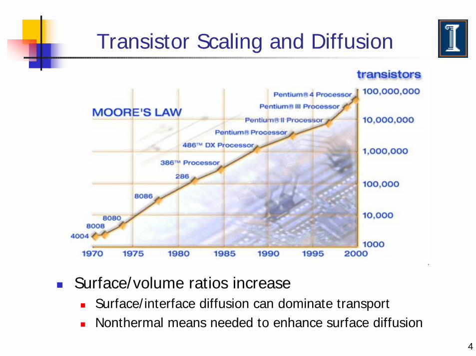
Transistor Scaling and Diffusion
! Surface/volume ratios increase! Surface/interface diffusion can dominate transport! Nonthermal means needed to enhance surface diffusion

5
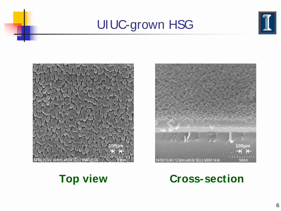
Application: Hemispherical Grained Silicon for DRAMs
! Formed by heating amorphous Si
! Crystallization begins at free surface
! Grains mushroom from surface by surface diffusion
! Rough surface increases capacitance/area
6
UIUC-grown HSG
Top view Cross-section
100µµµµm100µµµµm
7
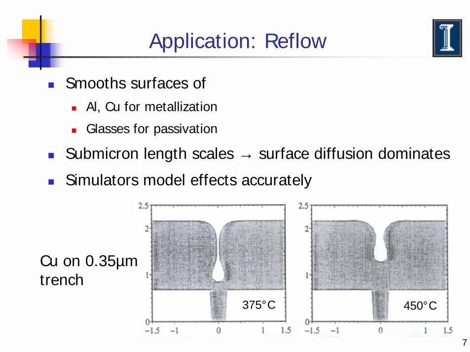
Application: Reflow
! Smooths surfaces of! Al, Cu for metallization
! Glasses for passivation
! Submicron length scales → surface diffusion dominates
! Simulators model effects accurately
Cu on 0.35µm trench
450°C375°C
8
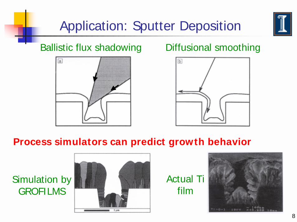
Application: Sputter DepositionBallistic flux shadowing Diffusional smoothing
Simulation byGROFILMS
Actual Ti film
Process simulators can predict growth behavior
9
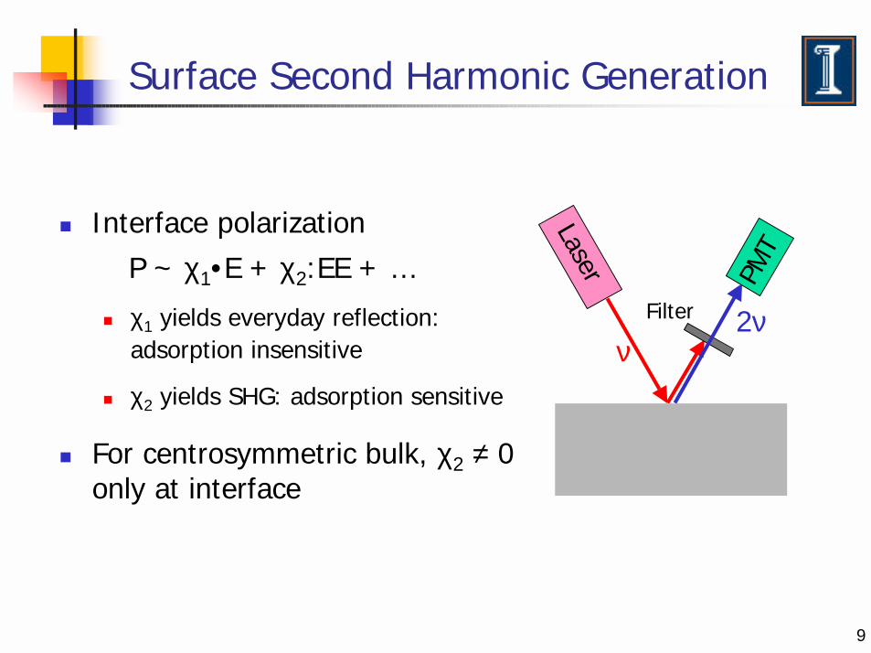
Surface Second Harmonic Generation
! Interface polarization P ~ χ1•E + χ2:EE + …
! χ1 yields everyday reflection: adsorption insensitive
! χ2 yields SHG: adsorption sensitive
! For centrosymmetric bulk, χ2 ≠ 0 only at interface
ν2ν
Laser PMT
Filter
10
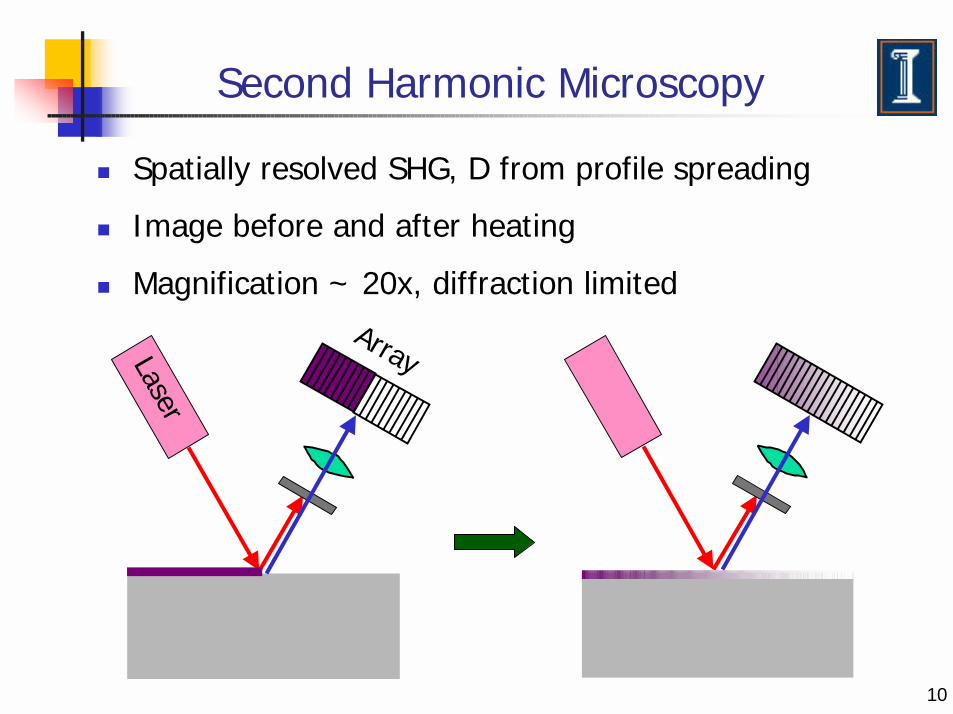
Second Harmonic Microscopy
Laser
Array
! Spatially resolved SHG, D from profile spreading
! Image before and after heating
! Magnification ~ 20x, diffraction limited

11
Experimental Set-up
! Signal averaging at 10 Hz takes ~ 5 min
! Imaging does not induce profile spreading
J. Opt. Soc. Am. B 10 (1993) 546
12
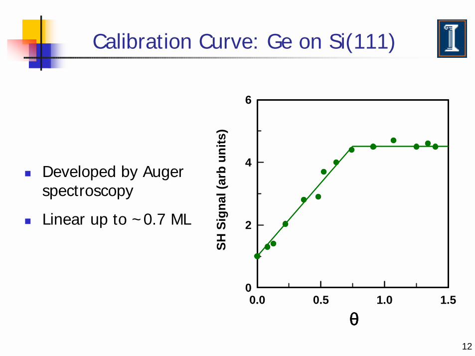
0.0 0.5 1.0 1.50
2
4
6
θθθθ
SH S
igna
l (ar
b un
its)
Calibration Curve: Ge on Si(111)
! Developed by Auger spectroscopy
! Linear up to ~0.7 ML
13
Diffused Step
SH S
igna
l (ar
b un
its)
Pixel Number
350 400 450 500 5500.2
0.4
0.6
0.8
1.0
1.2
Diffused Step
θ θθθ Ge
Position (µm)300 450 600 750
0.0
0.2
0.4
0.6
Second Harmonic Images: Ge on Si(111)
Unprocessed profiles After image processing
14
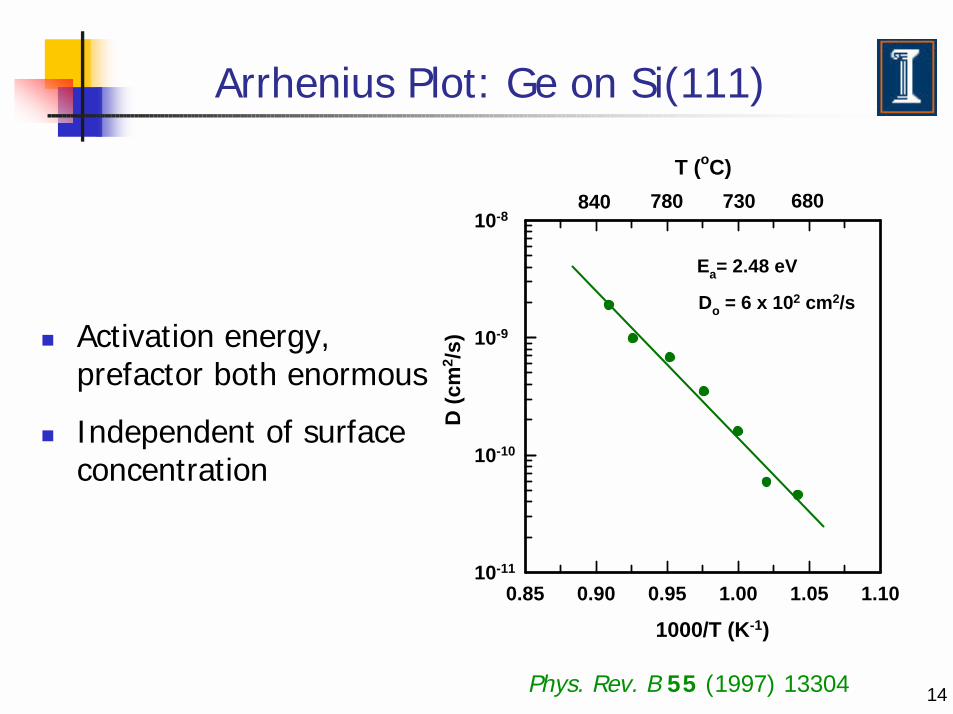
T (oC)
D (c
m2 /s
)
1000/T (K-1)0.85 0.90 0.95 1.00 1.05 1.10
10-11
10-10
10-9
10-8
Do = 6 x 102 cm2/s
840 780 730 680
Ea= 2.48 eV
Arrhenius Plot: Ge on Si(111)
Phys. Rev. B 55 (1997) 13304
! Activation energy, prefactor both enormous
! Independent of surface concentration

15
Surface Diffusion Physics on Si at High T
" Composite surface diffusivity DM depends on:
" Mobility of mobile species
" Number of mobile species
" Etotal = Ehop + Epair formation ≈ 0.5 + 2.0 eV
" Do,total = (10-3 cm2/s) exp(∆Spair formation/kT)
≈ 106
16
Illumination-Influenced Surface Diffusion: Experimental Results
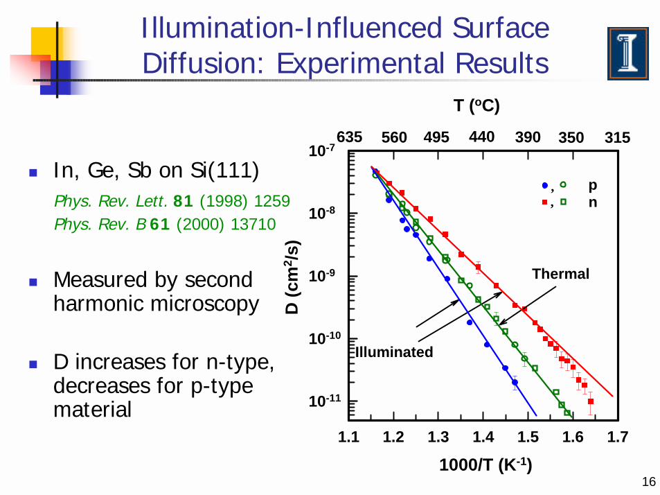
390440 350 315635 560 495
T (oC)
D (c
m2 /s
)
1000/T (K-1)1.1 1.2 1.3 1.4 1.5 1.6 1.7
10-11
10-10
10-9
10-8
10-7
,, n
p
Illuminated
Thermal
! In, Ge, Sb on Si(111)Phys. Rev. Lett. 81 (1998) 1259Phys. Rev. B 61 (2000) 13710
! Measured by second harmonic microscopy
! D increases for n-type, decreases for p-type material

17
Surface Diffusion Physics on Si at High T
" Composite surface diffusivity DM depends on:
" Number of vacancies,mobile atoms
" Numbers depend on charge state
" For all adsorbates (at 2 W/cm2):" Ediff changes by 0.3 eV" Prefactor changes by ~ 100×
" Invariance with adsorbate suggests underlying commonality: Ionization of surface vacancies

18
Quantum Calculations
MotivationCharge states of Si surface vacancies unknown, difficult to measure experimentally
Quantum calculations can predict vacancy energy levels and formation energies
ImplementationAb-initio pseudopotential calculation using DFT
Supercell approach, periodic boundary conditions
CASTEP software (Accelrys Inc.)
Si(100)-(2×1) surface: mono- and divacancy
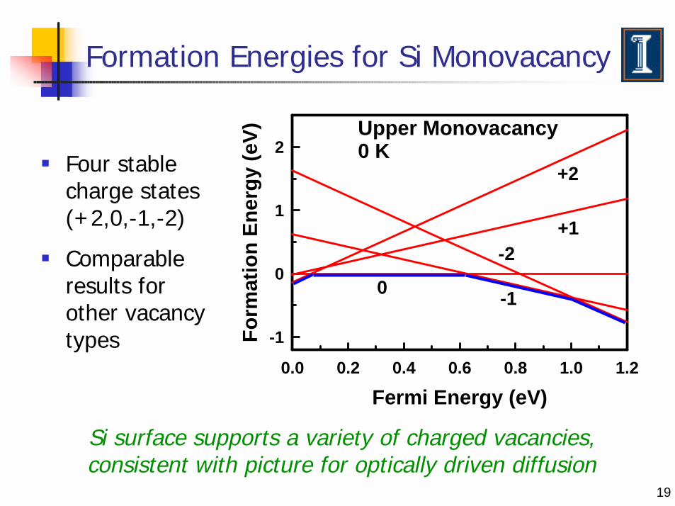
19
Formation Energies for Si Monovacancy
" Four stable charge states (+2,0,-1,-2)
" Comparable results for other vacancy types
Si surface supports a variety of charged vacancies, consistent with picture for optically driven diffusion
Fermi Energy (eV)0.0 0.2 0.4 0.6 0.8 1.0 1.2
Form
atio
n En
ergy
(eV)
-1
0
1
2
-2
-1
+2
+1
0
Upper Monovacancy0 K

20
Analogies between Surface, Bulk Diffusion
Bulk Surface
Hopping Interstitial motion Adatom motion
diffusion Vacancy motion Vacancy motion
Kick-in/kick-out Exchange
Overall mass Clustering Islanding transport Vacancy-interstitial
formation Vacancy-adatom
formation
Point defect ionization
Point defect ionization
21
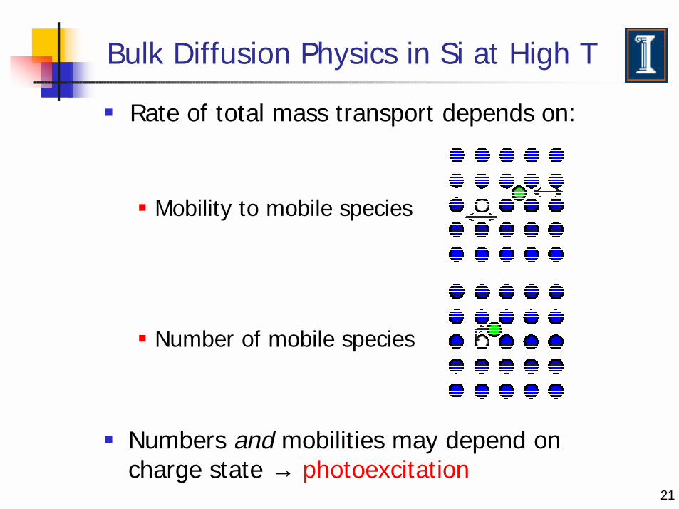
Bulk Diffusion Physics in Si at High T
" Rate of total mass transport depends on:
" Mobility to mobile species
" Number of mobile species
" Numbers and mobilities may depend on charge state → photoexcitation
22
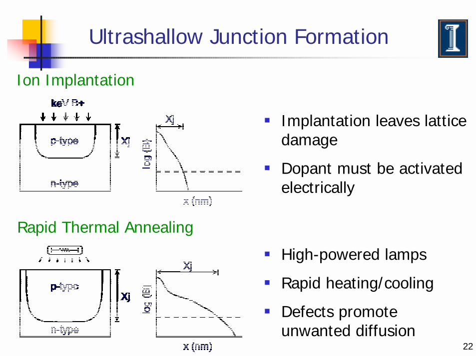
Ultrashallow Junction Formation
" Implantation leaves lattice damage
" Dopant must be activated electrically
" High-powered lamps
" Rapid heating/cooling
" Defects promote unwanted diffusion
Ion Implantation
Rapid Thermal Annealing

23
Measurement of Bulk Diffusion
" Isotopically-depleted layer grown epitaxially via LPCVD
30Si28Si (natural)
30Si (depleted)
30Si (natural)
28Si (enriched)
" 30Si step profile created
" Doping level uniform (eliminates drift effects)
24
1e+17
1e+18
1e+19
1e+20
1e+21
1e+22
100 200 300 400 500 600
x (nm)
30Si
(cm
-3)
hvdarkas-grown
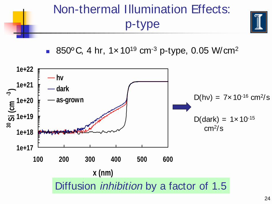
Non-thermal Illumination Effects: p-type
! 850ºC, 4 hr, 1×1019 cm-3 p-type, 0.05 W/cm2
D(hν) = 7×10-16 cm2/s
D(dark) = 1×10-15
cm2/s
Diffusion inhibition by a factor of 1.5
25
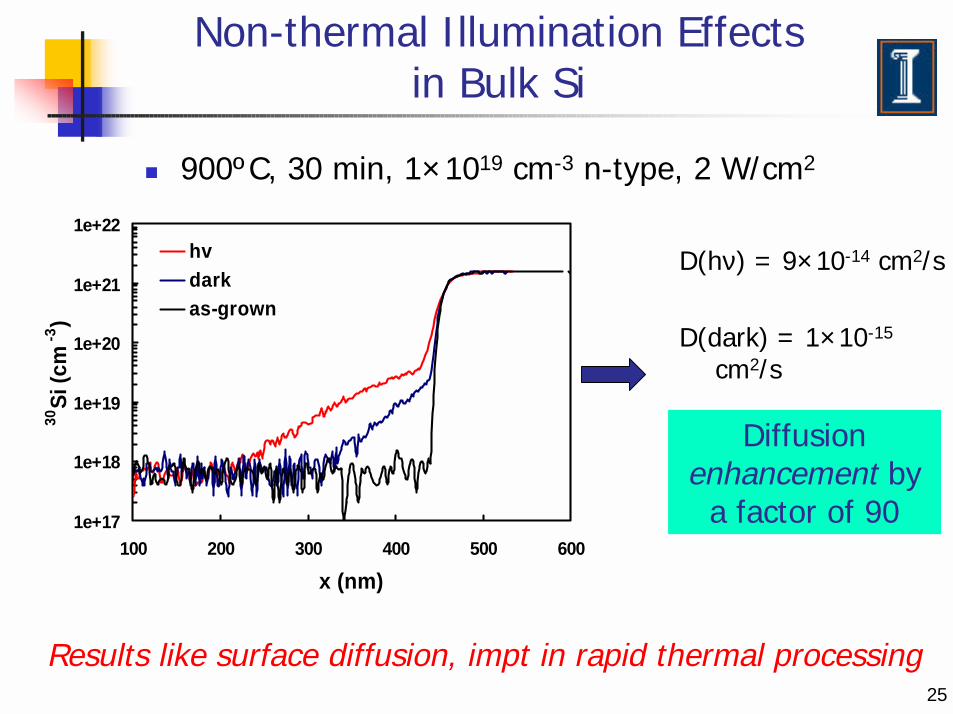
Non-thermal Illumination Effects in Bulk Si
! 900ºC, 30 min, 1×1019 cm-3 n-type, 2 W/cm2
1e+17
1e+18
1e+19
1e+20
1e+21
1e+22
100 200 300 400 500 600
x (nm)
30Si
(cm
-3)
hvdarkas-grown
D(hν) = 9×10-14 cm2/s
D(dark) = 1×10-15
cm2/s
Diffusion enhancement by
a factor of 90
Results like surface diffusion, impt in rapid thermal processing

26
Application for Nonthermally-Driven Diffusion: Nanoparticle Growth on a-Si
• Anneal (645°C)
75 sec 90 sec 105 sec
Motivated by Hemispherical Grained Si growth for DRAMs
• Grow amorphous Si by chemical vapor deposition
• Grain growth rate may be nonthermally influenced
27
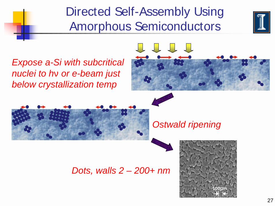
Directed Self-Assembly Using Amorphous Semiconductors
Ostwald ripening
Expose a-Si with subcritical nuclei to hν or e-beam just below crystallization temp
100µµµµm
Dots, walls 2 – 200+ nm
28
Applications of Self-Assembly Method
! Nonvolatile memory at high density, low power! Sensors! Photonic band gap materials! Flat panel displays! Solar cells! On-chip nanopore devices for probing electrical
activity of biological molecules
Particle arrays, walls, narrow pores for:
29
Diffusion at Solid Interfaces: Copper in Interconnect Structures
! Diffusion of Cu at interfaces remains uninvestigated! Barrier layers
! Etch stops
! Interlayer dielectrics
! Could be major means of transport during processing, use
! Problems with line-to-line shorting, Si deep levels…
We seek to make first measurements of Cu diffusion at these interfaces
30
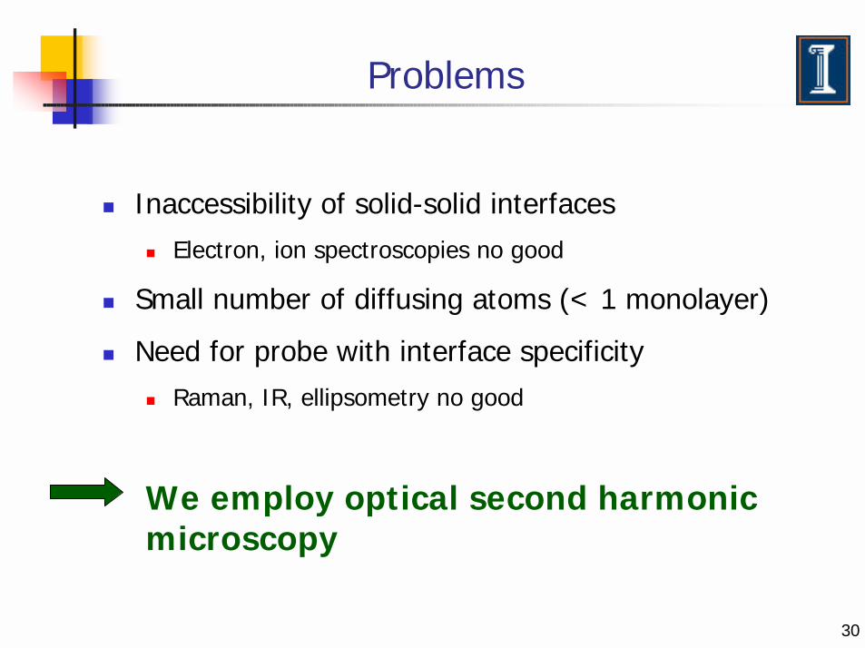
Problems
! Inaccessibility of solid-solid interfaces! Electron, ion spectroscopies no good
! Small number of diffusing atoms (< 1 monolayer)
! Need for probe with interface specificity! Raman, IR, ellipsometry no good
We employ optical second harmonic microscopy
31
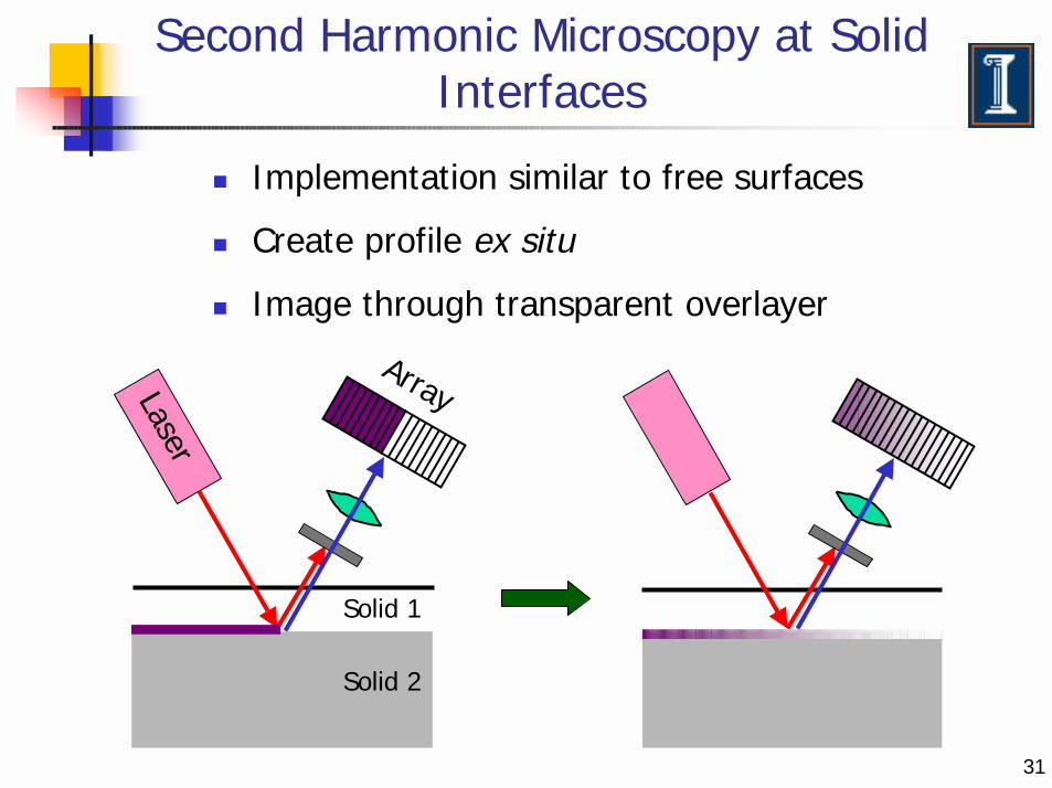
Second Harmonic Microscopy at Solid Interfaces
Laser
Array
Solid 1
Solid 2
! Implementation similar to free surfaces
! Create profile ex situ
! Image through transparent overlayer

32
Measurement Concept
! Position Cu source near one end of interface
! Heat structure
! Freeze concentration profile and image
! Structure below made at Chartered Semiconductor
SiO2
Si3N4
Si3N4
Cu! 5 nm Ta
separates Cu from ILD

33
Preliminary Imaging Results
700°C
! Profiles are very flat! Diffusion through Ta barrier rate limiting
! Diffusion at upper or lower interface?
34
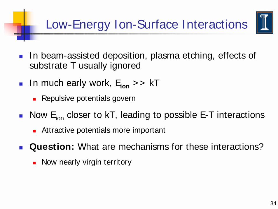
Low-Energy Ion-Surface Interactions
! In beam-assisted deposition, plasma etching, effects of substrate T usually ignored
! In much early work, Eion >> kT
! Repulsive potentials govern
! Now Eion closer to kT, leading to possible E-T interactions
! Attractive potentials more important
! Question: What are mechanisms for these interactions?
! Now nearly virgin territory
35
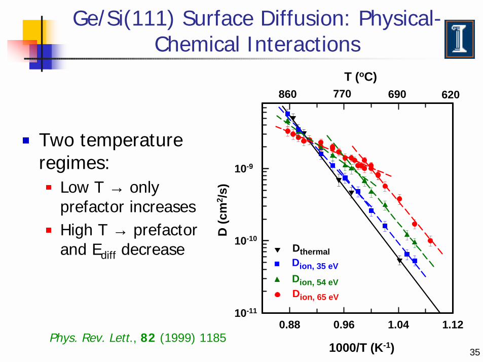
Ge/Si(111) Surface Diffusion: Physical-Chemical Interactions
Dion, 54 eV
860 770 690 620T (oC)
D (c
m2 /s
)
1000/T (K-1)
0.88 0.96 1.04 1.1210-11
10-10
10-9
Dion, 35 eV
Dthermal
Dion, 65 eV
Two temperature regimes:
Low T → only prefactor increasesHigh T → prefactor and Ediff decrease
Phys. Rev. Lett., 82 (1999) 1185
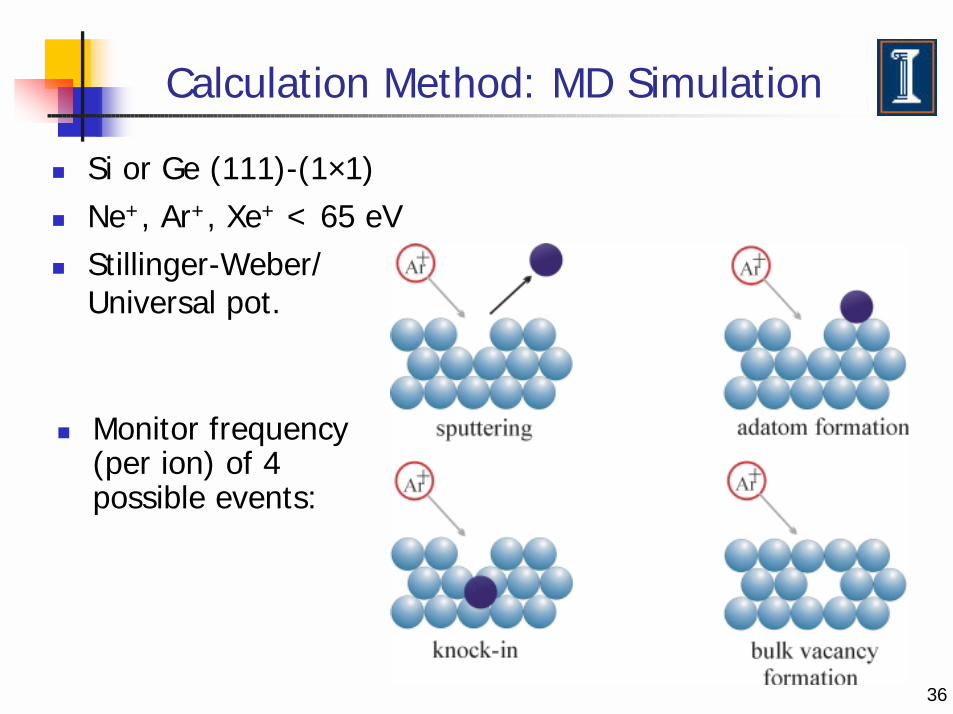
36
Calculation Method: MD Simulation
! Si or Ge (111)-(1×1)! Ne+, Ar+, Xe+ < 65 eV! Stillinger-Weber/
Universal pot.
! Monitor frequency (per ion) of 4 possible events:

37
Energy Effects, Constant T
E (eV)10 20 30 40 50 60 70
Per
Impa
ct P
roba
bilit
ies
0.0
0.1
0.2
0.3
0.4 SputteringAdatom formationKnockinBulk vacancy
Ar-Si, 1100K
Thresholds
Determine EThres where f ≤ 0.01
Fits use f = A (E1/2 – EThres1/2)
38
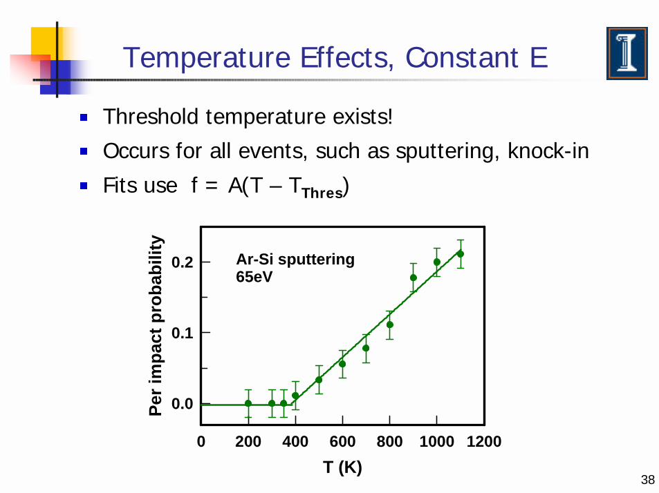
Temperature Effects, Constant E
T (K)0 200 400 600 800 1000 1200
Per i
mpa
ct p
roba
bilit
y
0.0
0.1
0.2 Ar-Si sputtering65eV
Threshold temperature exists!
Occurs for all events, such as sputtering, knock-in
Fits use f = A(T – TThres)

39
At Threshold, T and Ion Energy are Coupled
T (K)0 200 400 600 800 1000 1200
E Thre
s(eV)
0
20
40
60
80
Si
Ge
Direct trade-off between E and TETotal = σkT + EThres (new result!)
~100eV ~10-65eV ~10-65eV
Large amplification factor σ ~ 103
Ar-Si sputtering

40
Physics: Ion Mass Variation
Atomic Number
0 10 20 30 40 50 60
E Tota
l(eV)
80
120
160
200
240
σ σσσ
-2400
-2000
-1600
-1200
-800
-400
(Ne) (Ar) (Xe)
Si Sputtering
Look for “standard” momentum matching effectsExpect big variation with mass, but observe little

41
Chemistry: Substrate Variation
T (K)0 200 400 600 800 1000 1200
E Thre
s(eV)
0
20
40
60
80
Si
Ge
σ (slope) invariant
ETotal (intercept) scales with cohesive energy, melting temp
! Look for bond strength effects
42
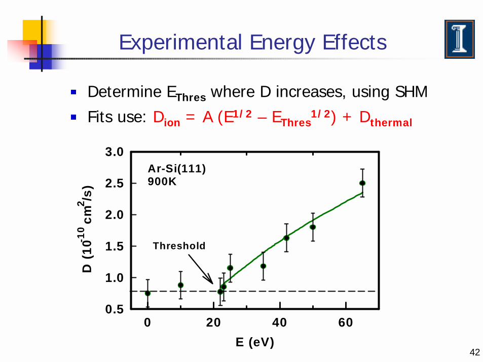
Experimental Energy Effects
E (eV)0 20 40 60
D (1
0-10 c
m2 /s
)
0.5
1.0
1.5
2.0
2.5
3.0Ar-Si(111) 900K
Threshold
Determine EThres where D increases, using SHM
Fits use: Dion = A (E1/2 – EThres1/2) + Dthermal

43
E-T Coupling Strength Matches Simulation
T (K)880 920 960 1000 1040
E Thre
s (eV
)
12
14
16
18
20
22
24
Ar-Si
ETotal σσσσ
Sim. 70 to 100 700 Expt. 110 1200
44
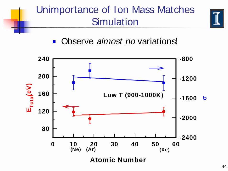
Unimportance of Ion Mass Matches Simulation
Atomic Number
0 10 20 30 40 50 60
E Tota
l(eV
)
80
120
160
200
240
σ σσσ
-2400
-2000
-1600
-1200
-800
(Ne) (Ar) (Xe)
Low T (900-1000K)
Observe almost no variations!
45
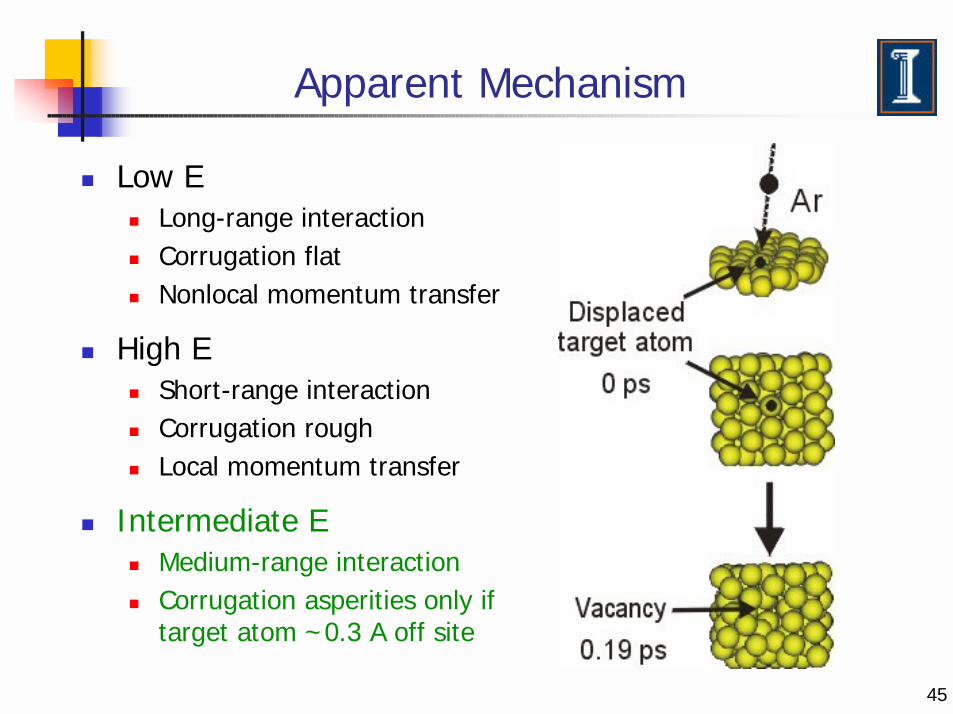
Apparent Mechanism
! Low E! Long-range interaction! Corrugation flat! Nonlocal momentum transfer
! High E! Short-range interaction! Corrugation rough! Local momentum transfer
! Intermediate E! Medium-range interaction! Corrugation asperities only if
target atom ~0.3 A off site

46
Summary
! New, nonthermal ways (hν, ions) to transport semiconductor atoms have come to light
! Numerous applications in microelectronic processing (RTP, dry etching, ion-assisted deposition) and nanotechnology
! Solid interfaces SHM imaging demonstrated

47
Acknowledgements to:
! Postdocs! Harry Ho Yeung Chan
! Graduate Students! Kapil Dev! Rod Ditchfield! Mike Jung! Diana Llera-Hurlburt! Shih Hwee Tey! Mike Wang


