
Progress with 2D Microstrip Detectors with Polycrystalline Silicon Electrodes
19th RD50 WorkshopNovember 23th CERN, Geneva
D. Bassignana, M. Lozano, G. Pellegrini, D. Quirion CNM-IMB (CSIC) M. Fernández, R. Jaramillo, F.J. Muñoz, I. Vila IFCA (CSIC-UC)

Outline— Introduction to charge-division concept in
microstrip sensors.— New sensor prototypes: signal processing
electronics.— Experimental arrangement: NIR laser & Test beam
characterization— SPICE sensor equivalent circuit vs. data: position
error studies— Sensor prototypes with integrated signal routing.— Summary and outlook
I.Vila, [email protected] - 19th RD50 workshop,23th Nov, Geneva 2011. 2

Charge-Division Concept in ustrip Sensors (1)
— Charge division used in wire chambers to determine the coordinate along the sensing wire.
— Same concept with conventional microstrips with slightly resistive electrodes (doped polysilicon)
3I.Vila, [email protected] - 19th RD50 workshop,23th Nov,
Geneva 2011.
Fractional Position≡ y /L=S2/(S1+S 2)
L
y

Charge-Division Concept in ustrip Sensors (2)— First proposed by Radeka (TNS Vol. 21, 1964)
_ Microstrip electrode as RC dispersive line._ Position dependent ballistic deficit.
— Optimization of the signal processing electronics shaping time (about one third of the detectors RC constant)
— Fractional position resolution independent of strip resistivity— Recently Radeka’s formulation validated @ SCIPP against
electronic circuit emulator (NIM A (2011) 646 118)
4I.Vila, [email protected] - 19th RD50 workshop,23th Nov,
Geneva 2011.

New Prototypes from CNM— One year ago very promising results on CNM’s first
prototypes with integrated on sensor signal routing for single-end readout ( affected by parasitic couplings, see later in this talk).
— Now presenting results on two new prototypes with double-end readout.
5I.Vila, [email protected] - 19th RD50 workshop,23th Nov,
Geneva 2011.
Strip:length =20 mmwidth =20 um
Pitches:Implant=80 umreadout= 80 um
Electrode:R/um = 2.8 Ohms/umR/um = 12.2 Ohms/um
Beatle chip

Signal Processing: shaping time issue— Electrodes as RC dispersive lines: attenuated and
delayed signals, moreover serial noise is increased (larger shaping times favored)
— But, suppressing parallel noise contribution requires smaller shaping times.
— Trade-off: shaping time optimized for a given RC characteristic ( about 1/3 of the RC from Radeka)
— ALIBAVA readout has a fixed 25ns shaping time (tshape)
Is this a sensible tshape for our prototype sensors?
Is the response linearity preserved?Spice simulation: sensor+signal processing electronics
6I.Vila, [email protected] - 19th RD50 workshop,23th Nov,
Geneva 2011.

Spice simulation (1): Equivalent Circuit— Detector cell model
including five consecutive strips.
— Total sensor: periodic structure composed of 80 cells.
— Realistic parameters (from sensor electrical characterization)
— Already validated microstrip simulation.
— charge sensitive preamplifier + CR-RC filter, which peaking time 25 ns.
7I.Vila, [email protected] - 19th RD50 workshop,23th Nov,
Geneva 2011.

SPICE Simulation (2): Signal Propagation.
— Charge injected at different strips positions.
— Current shapes at the entrance of the charge pream after propagation.
— As expected: delayed and attenuated pulses
— Worst case (most resistive):tshape ≥ Signal rise time
8I.Vila, [email protected] - 19th RD50 workshop,23th Nov,
Geneva 2011.

SPICE Simulation (3): Linear Response— sub-optimal tshape but still good enough to preserve
the linear response, significantly better for the low resistance prototype
9I.Vila, [email protected] - 19th RD50 workshop,23th Nov,
Geneva 2011.
Greenline is ideal Fractional Position≡S2/ (S 1+S 2)

What about the real data?
GOALS: — NIR Laser: Experimental validation of the
Charge-Division concept in a full-fledged microstrip sensor.
— NIR Laser: Benchmarking of the spice simulation as a designer tool for future prototypes.
— SPS pions: SNR studies for MIP particles, aka, feasibility of technology for HEP trackers.
10I.Vila, [email protected] - 19th RD50 workshop,23th Nov,
Geneva 2011.


Laser Data: Pulse propagation— High resistivity sensor: 12.2 Ω/μm, RC = 450ns— Laser longitudinal scan & sampling time scan to
measure the full pulse shape at each position along the strip.
— Signal out of shaper is delayed & attenuated
12I.Vila, [email protected] - 19th RD50 workshop,23th Nov,
Geneva 2011.

Data vs. Simulation: Fractional position (1)— High resistivity sensor: 12.2 Ω/μm, RC = 450ns
13I.Vila, [email protected] - 19th RD50 workshop,23th Nov,
Geneva 2011.

Data vs. Simulation: Fractional position (2)
— Low resistivity prototype: 2.8 Ω/μm, RC = 100ns
14I.Vila, [email protected] - 19th RD50 workshop,23th Nov,
Geneva 2011.

Laser Data: Noise Study— Errors computed propagating Radeka’s analytical expressions.— A Resistive electrode introduces and anti-correlation between
the noise excursions at both end of the strip.— Laser fluctuation introduces a correlated components in the
noise excursions— The actual noise correlation between the two ends of the strips
at each scanning point will depend on which of the two components dominates.
15I.Vila, [email protected] - 19th RD50 workshop,23th Nov,
Geneva 2011.
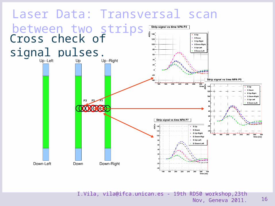
Laser Data: Transversal scan between two strips
Cross check of signal pulses.
16I.Vila, [email protected] - 19th RD50 workshop,23th Nov,
Geneva 2011.

Test beam Data: beam profiles and SNR— Initial & still preliminary results on last year test beams at SPS
120 GeV pion beams (using both ALIBAVA and APV25 Daq)
17I.Vila, [email protected] - 19th RD50 workshop,23th Nov,
Geneva 2011.

Signal routing integrated on sensor: issue & proposal.— HEP Tracking use case
requires local in-situ cluster finding
— Charge readout at both ends of the strip to be add-up to find hit clusters.
— Cheap and easy technological solution: integrate on the sensor a extra metal via for routing all the signals to one single end.
18I.Vila, [email protected] - 19th RD50 workshop,23th Nov,
Geneva 2011.

Prototypes: parasitic couplings— Induced signal on metallic vias superposed to “direct signal”
propagated through polysilicon electrode.— Induced signal constant delay & shape with respect to the laser
pulse while signal pulse delay increases with longer propagation distance along the polysilicon strip.
— Position dependent bias of the signal routed through the via.
19I.Vila, [email protected] - 19th RD50 workshop,23th Nov,
Geneva 2011.

Parasitic couplings (2): Offline Correction
— Offline subtraction of induction bias in the right direction but not enough.
— Relatively easy technological solution: increase oxide thickness or go to a double metal process.
20I.Vila, [email protected] - 19th RD50 workshop,23th Nov,
Geneva 2011.
Summary and Outlook— Feasibility of the charge-division method in microstrip
sensors has been demonstrated (radiation resistance?)— Excellent agreement between data and electronic
simulation to be used as sensor designing tool.— Full-fledged baby-sensors tested at SPS pion beam
deliver a SNR of around 20.— A technological implementation for a simplified
engineering integration of the sensors with the readout hybrid has been proposed.
— A new prototype in preparation to improve the implementation of the sensors with integrated signal vias.
21I.Vila, [email protected] - 19th RD50 workshop,23th Nov,
Geneva 2011.
arXiv:1106.5405v2

THANK YOU FOR YOU ATTENTION !And especial thanks to:
22I.Vila, [email protected] - 19th RD50 workshop,23th Nov,
Geneva 2011.

BACK UP

Injected pulses for Spice simulation
24I.Vila, [email protected] - 19th RD50 workshop,23th Nov,
Geneva 2011.


Test beam Data (2): beam profiles with ALIBAVA— VERY VERY PRELIMINARY, still work in progress.
26I.Vila, [email protected] - 19th RD50 workshop,23th Nov,
Geneva 2011.


