
VDS Tjmax
Ω•
•
•
•
•
•
G
G
TC
TC
tp Tjmax
VDD
Tjmax
VDD
EAR
Tjmax
Gate source voltage static VGS
VGS ±Ptot
8 02 11Rev. 2.6 P
Reverse diode dv/dt dv/dt 15 V/ns4)
Please note the new package dimensions arccording to PCN 2009-134-A

VDS Tj
RthJC
RthJA
wavesoldering
V(BR)DSS VGS
VGS
µΑ VGS VDS
VDS VGS
Tj
Tj
VGS VDS
VGS
Tj
Tj
Ω
RG
8 02 11Rev. 2.6 P 2
Please note the new package dimensions arccording to PCN 2009-134-A
Tj
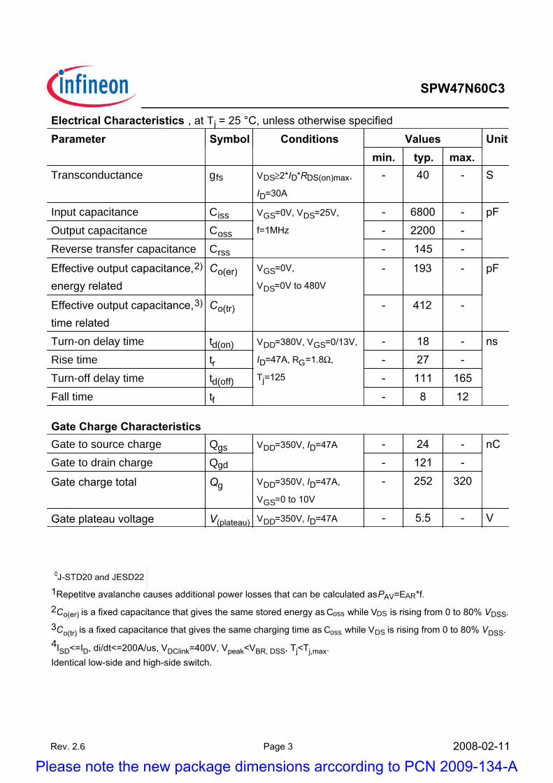
Transconductance gfs VDS≥
Input capacitance Ciss VGS VDS
fOutput capacitance Coss
Reverse transfer capacitance Crss
VGS
VDS
Turn-on delay time td(on) VDD VGS
RG Ω
Tj
Rise time trTurn-off delay time td(off)
Fall time tf
Gate to source charge Qgs VDD
Gate to drain charge Qgd
VDD
VGS
VDD
EAR f
Coss VDS
Coss VDS
8 02 11Rev. 2.6 P 3
4ISD<=ID, di/dt<=200A/us, VDClink=400V, Vpeak<VBR, DSS, Tj<Tj,max. Identical low-side and high-side switch.
Please note the new package dimensions arccording to PCN 2009-134-A

Tj
TC
Inverse diode direct current,
pulsed
ISM
VGS
Reverse recovery time trr VR
diF/dtReverse recovery charge Qrr
Peak reverse recovery current Irrm
8 02 11Rev. 2.6 P 4
Please note the new package dimensions arccording to PCN 2009-134-A

TC
TC
Pto
t
TC
VDS
tp
VDS Tj
VGS
VDS
8 02 11Rev. 2.6 P 5
Please note the new package dimensions arccording to PCN 2009-134-A

VDS Tj
VGS
VDS
f
Tj VGS
Ω
VGS
Tj
Ω
≥
VGS
8 02 11Rev. 2.6 P 6
Please note the new package dimensions arccording to PCN 2009-134-A

VGS
VG
S VDS max
VDS max I F
di/dt RG Tj
VDS VGS
ΩRG
di/d
t
RG Tj
VDS VGS
8 02 11Rev. 2.6 P 7
Please note the new package dimensions arccording to PCN 2009-134-A

Tj
VDS VGS RG Ωdv/dt RG Tj
VDS VGS
ΩRG
dv/d
t
Tj
VDS VGS RG ΩRG Tj
VDS VGS
ΩRG
8 02 11Rev. 2.6 P 8
Please note the new package dimensions arccording to PCN 2009-134-A

Tj ≤Tj
VDD
Tj
V(BR)DSS Tj
Tj
V(B
R)D
SS
f
EAR
f
8 02 11Rev. 2.6 P 9
Please note the new package dimensions arccording to PCN 2009-134-A

VDS
VGS
VDS
Coss
f VDS
VDS
Tj
8 02 11Rev. 2.6 P 0
Please note the new package dimensions arccording to PCN 2009-134-A

8 02 11Rev. 2.6 P 1
Please note the new package dimensions arccording to PCN 2009-134-A

8 02 11Rev. 2.6 P 2
47 6
G
Please note the new package dimensions arccording to PCN 2009-134-A
Published by Infineon Technologies AG 81726 Munich, Germany © 2008 Infineon Technologies AG All Rights Reserved. Legal Disclaimer The information given in this document shall in no event be regarded as a guarantee of conditions or characteristics. With respect to any examples or hints given herein, any typical values stated herein and/or any information regarding the application of the device, Infineon Technologies hereby disclaims any and all warranties and liabilities of any kind, including without limitation, warranties of non-infringement of intellectual property rights of any third party. Information For further information on technology, delivery terms and conditions and prices, please contact the nearest Infineon Technologies Office (www.infineon.com). Warnings Due to technical requirements, components may contain dangerous substances. For information on the types in question, please contact the nearest Infineon Technologies Office. Infineon Technologies components may be used in life-support devices or systems only with the express written approval of Infineon Technologies, if a failure of such components can reasonably be expected to cause the failure of that life-support device or system or to affect the safety or effectiveness of that device or system. Life support devices or systems are intended to be implanted in the human body or to support and/or maintain and sustain and/or protect human life. If they fail, it is reasonable to assume that the health of the user or other persons may be endangered.
8 02 11Rev. 2.6 P 3
Please note the new package dimensions arccording to PCN 2009-134-A

Data sheet erratumPCN 2009-134-A
New package outlines TO-247
Final Data Sheet Erratum Rev. 2.0, 2010-02-01
1 New package outlines TO-247Assembly capacity extension for CoolMOSTM technology products assembled in lead-free package PG-TO247-3 at subcontractor ASE (Weihai) Inc., China (Changes are marked in blue.)
Figure 1 Outlines TO-247, dimensions in mm/inches


