Duane Boning - ICMTS 2003 1 MIT-MTL
Pattern Dependent Characterizationof Copper Interconnect
Prof. Duane Boning
Massachusetts Institute of TechnologyMicrosystems Technology Laboratories
http://www-mtl.mit.edu/Metrology
ICMTS Tutorial, March 2003
Duane Boning - ICMTS 2003 2 MIT-MTL
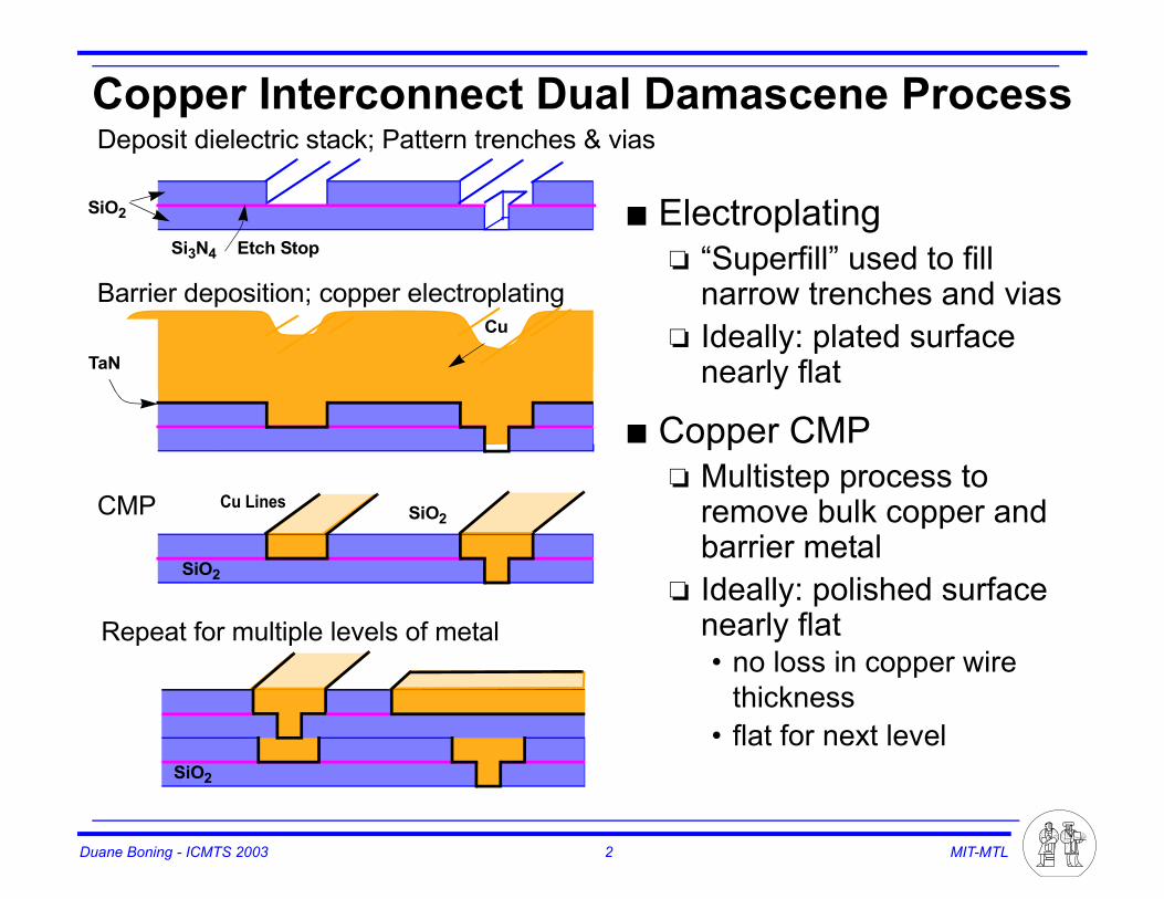
Copper Interconnect Dual Damascene ProcessDeposit dielectric stack; Pattern trenches & vias
Barrier deposition; copper electroplating
CMP
SiO2
SiO2
Si3N4 Etch Stop
SiO2
SiO2
SiO2
Cu
TaN
■ Electroplating❏ “Superfill” used to fill
narrow trenches and vias ❏ Ideally: plated surface
nearly flat
■ Copper CMP❏ Multistep process to
remove bulk copper and barrier metal
❏ Ideally: polished surface nearly flat • no loss in copper wire
thickness• flat for next level
Cu Lines
Repeat for multiple levels of metal

Duane Boning - ICMTS 2003 3 MIT-MTL
Copper Interconnect Problems■ Polishing stages: bulk polish, barrier polish, and overpolish
CMP Process and Problems
Oxide
Oxide
Dishing
Field OxideLoss
Erosion
Non-uniform plating
Oxide
CMP
Overpolish
Evolving Surface Profile
Duane Boning - ICMTS 2003 4 MIT-MTL
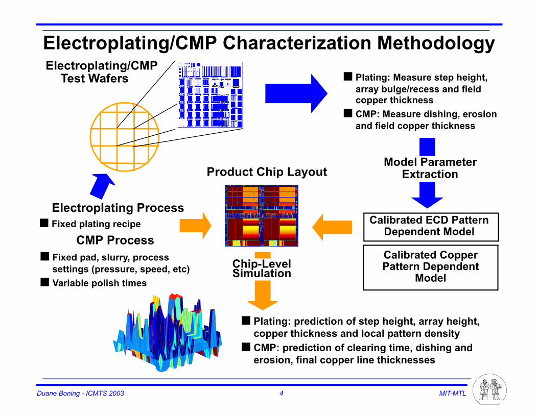
Electroplating/CMP Characterization Methodology
Electroplating Process■ Fixed plating recipe
Model ParameterExtraction
■ Plating: Measure step height, array bulge/recess and field copper thickness
■ CMP: Measure dishing, erosion and field copper thickness
Calibrated ECD Pattern Dependent Model
■ Plating: prediction of step height, array height, copper thickness and local pattern density
■ CMP: prediction of clearing time, dishing and erosion, final copper line thicknesses
Chip-LevelSimulation
Product Chip Layout
Electroplating/CMPTest Wafers
CMP Process■ Fixed pad, slurry, process
settings (pressure, speed, etc)■ Variable polish times
Calibrated Copper Pattern Dependent
Model
Duane Boning - ICMTS 2003 5 MIT-MTL
Outline■ Background
❏ Pattern dependent effects in plating and CMP
■ Copper CMP Characterization❏ Polishing Length Scales❏ Test Structure and Mask Design
• Single Layer Test Structures and Mask Design• Multilevel Test Structures and Mask Design
❏ Measurements and Analysis❏ Design Rule Generation❏ Chip Scale Modeling
■ Copper Electroplating Characterization
■ Conclusions
Duane Boning - ICMTS 2003 6 MIT-MTL
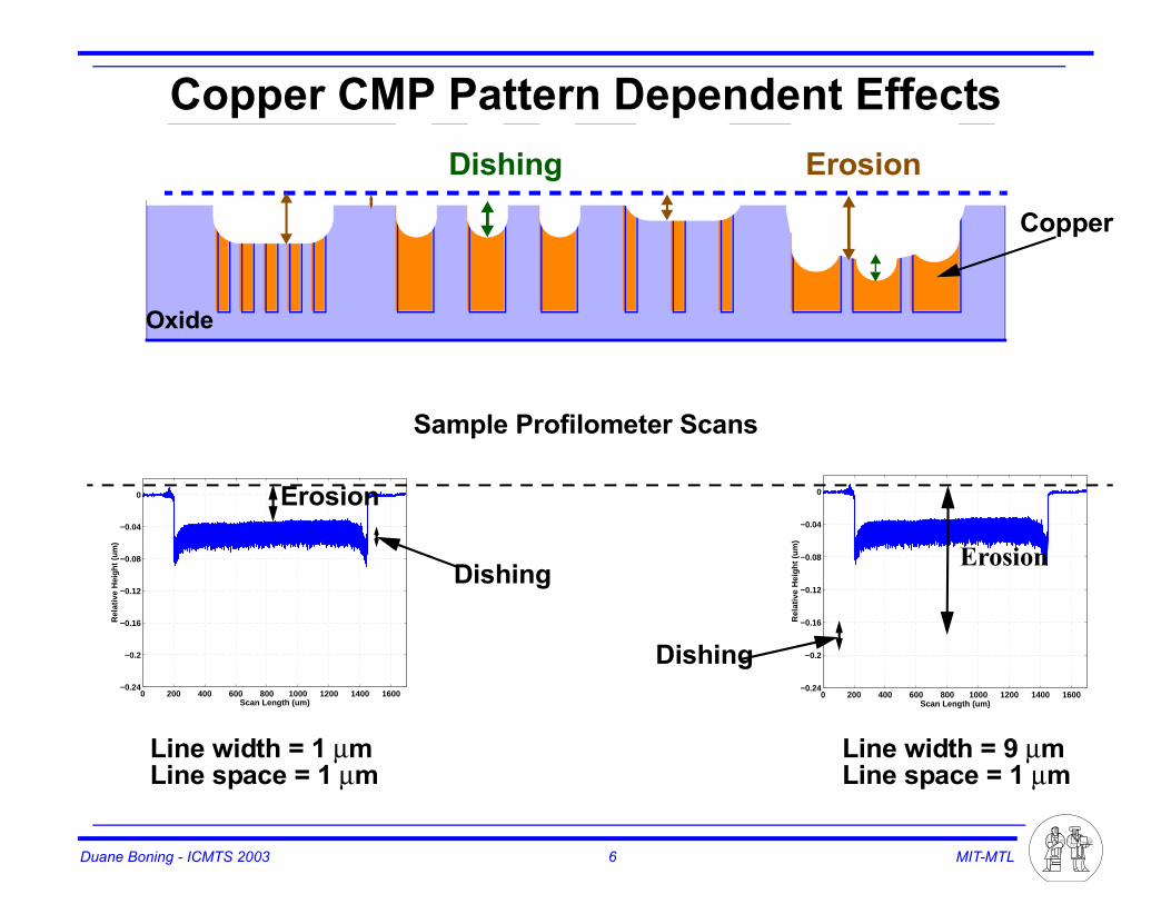
Copper CMP Pattern Dependent Effects
Oxide
Dishing Erosion
Copper
0 200 400 600 800 1000 1200 1400 1600−0.24
−0.2
−0.16
−0.12
−0.08
−0.04
0
Scan Length (um)
Rel
ativ
e H
eig
ht
(um
)
0 200 400 600 800 1000 1200 1400 1600−0.24
−0.2
−0.16
−0.12
−0.08
−0.04
0
Scan Length (um)
Rel
ativ
e H
eig
ht
(um
)
Erosion
Dishing
Erosion
Dishing
Sample Profilometer Scans
Line width = 1 µmLine space = 1 µm
Line width = 9 µmLine space = 1 µm
Duane Boning - ICMTS 2003 7 MIT-MTL
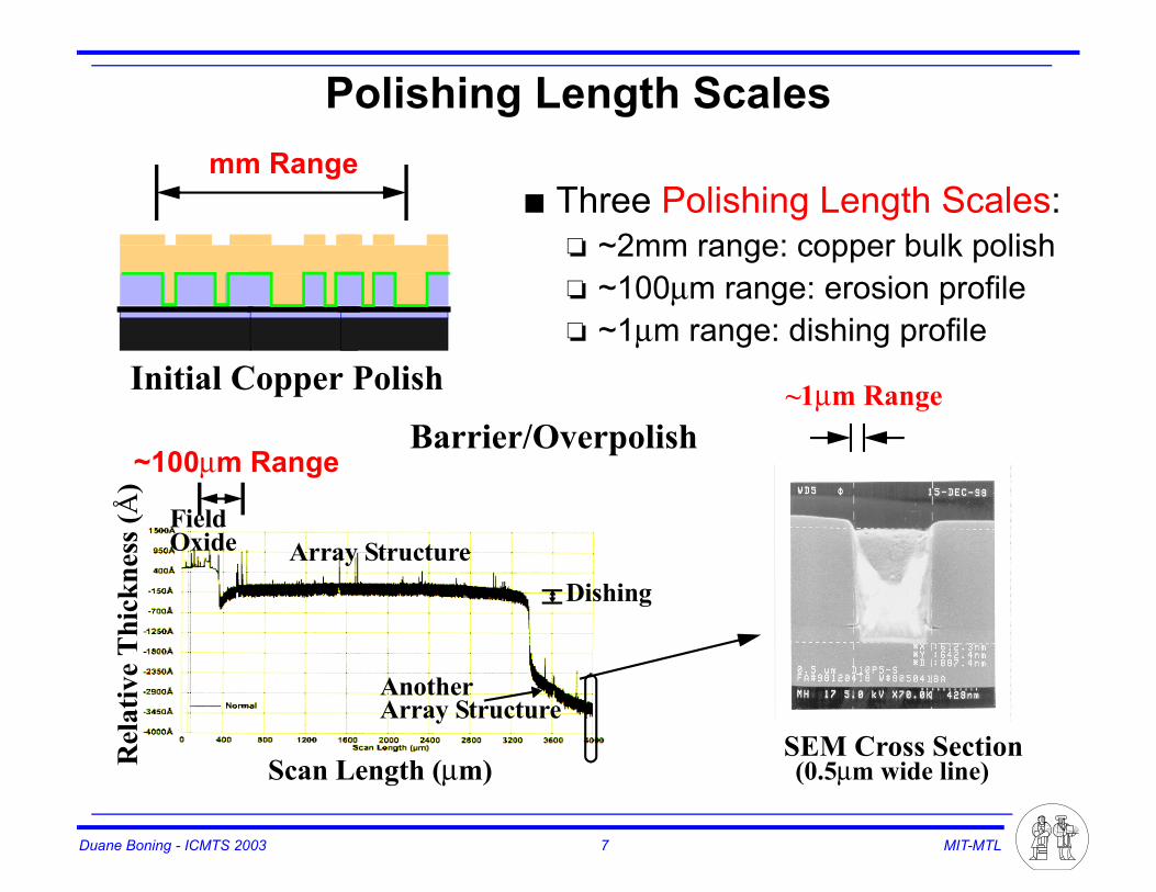
Polishing Length Scales
FieldArray Structure
AnotherArray Structure
Oxide
Dishing
Rel
ativ
e T
hick
ness
(Å)
Scan Length (µm)SEM Cross Section(0.5µm wide line)
mm Range
~100µm Range
~1µm RangeInitial Copper Polish
Barrier/Overpolish
■ Three Polishing Length Scales:❏ ~2mm range: copper bulk polish❏ ~100µm range: erosion profile❏ ~1µm range: dishing profile
Duane Boning - ICMTS 2003 8 MIT-MTL
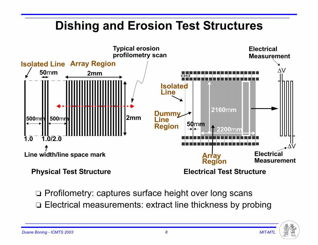
Dishing and Erosion Test Structures
Isolated Line Array Region
Line width/line space mark
500mm
50mm 2mm
2mm
1.0 1.0/2.0
500mm
IsolatedLine
DummyLine
ArrayRegion
0.5/4.5
Electrical
Electrical∆V
∆V
50mm2200mm
2160mm
Physical Test Structure Electrical Test Structure
Region
Measurement
Typical erosionprofilometry scan Measurement
❏ Profilometry: captures surface height over long scans❏ Electrical measurements: extract line thickness by probing

Duane Boning - ICMTS 2003 9 MIT-MTL
Dishing/Erosion Array Test Structures
(a) (b) (c)si
ngle
loop
loop
w/ d
umm
y
50%
den
sity
arr
a
(d)
■ Three Regions: b) Single loop: isolated linec) Small array: loop with surrounding dummy linesd) Large array: multiple taps along length of the array
■ Electrical Sampling: ❏ Each tap is a Van der Pauw structure: measure resistance❏ Uniform sampling: e.g. every 100 µm❏ Edge sampling: place more taps near the transition region
Duane Boning - ICMTS 2003 10 MIT-MTL
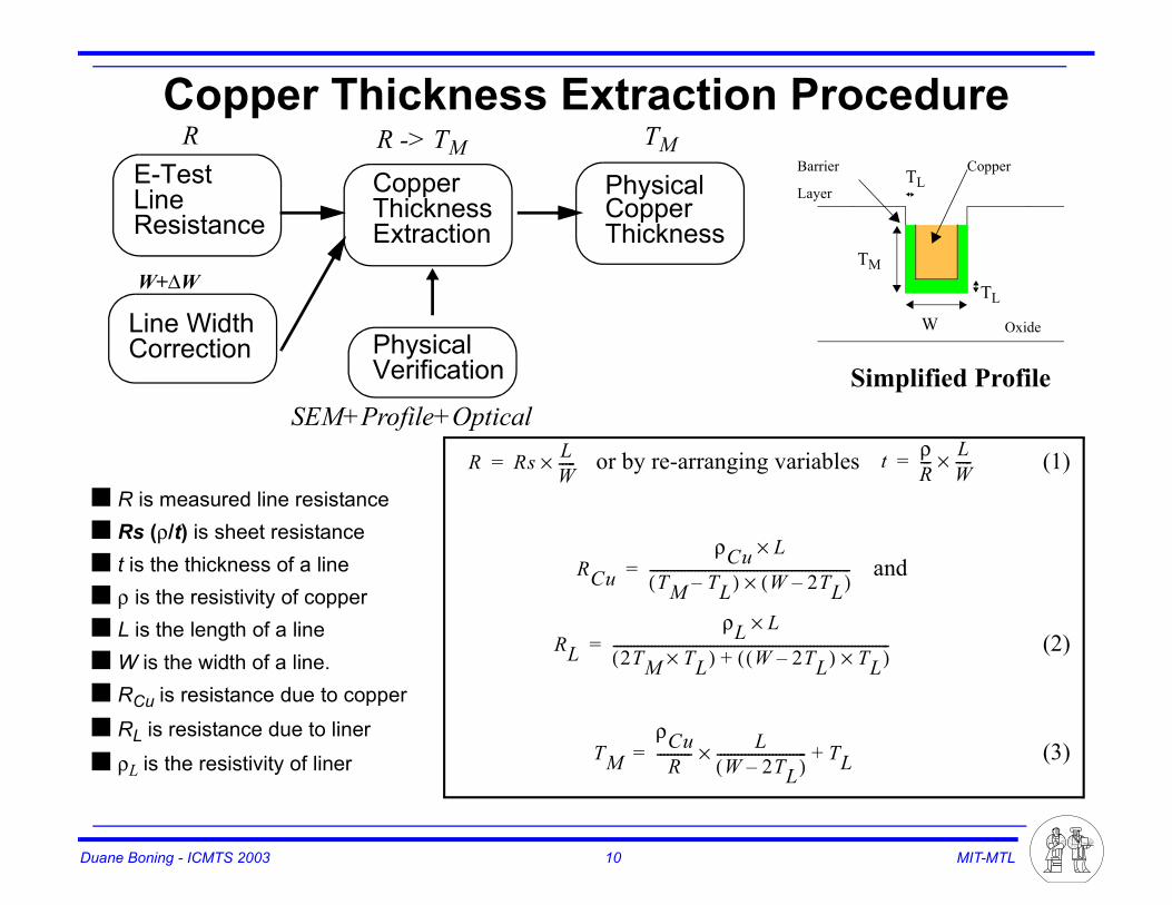
Copper Thickness Extraction ProcedureE-TestLineResistance
Line WidthCorrection
CopperThicknessExtraction
CopperThickness
Physical
PhysicalVerification
R
SEM+Profile+Optical
W+∆W
R -> TM TM
Oxide
TM
TL
TL
Copper
W
Barrier
Layer
Simplified Profile
■ R is measured line resistance■ Rs (ρ/t) is sheet resistance■ t is the thickness of a line■ ρ is the resistivity of copper■ L is the length of a line■ W is the width of a line.■ RCu is resistance due to copper
■ RL is resistance due to liner
■ ρL is the resistivity of liner
or by re-arranging variables (1)
and
(2)
(3)
R Rs LW-----×= t ρ
R---LW-----×=
RCuρCu L×
TM TL–( ) W 2TL–( )×----------------------------------------------------------=
RLρL L×
2TM TL×( ) W 2TL–( ) TL×( )+--------------------------------------------------------------------------------=
TMρCu
R---------- L
W 2TL–( )--------------------------× TL+=
Duane Boning - ICMTS 2003 11 MIT-MTL
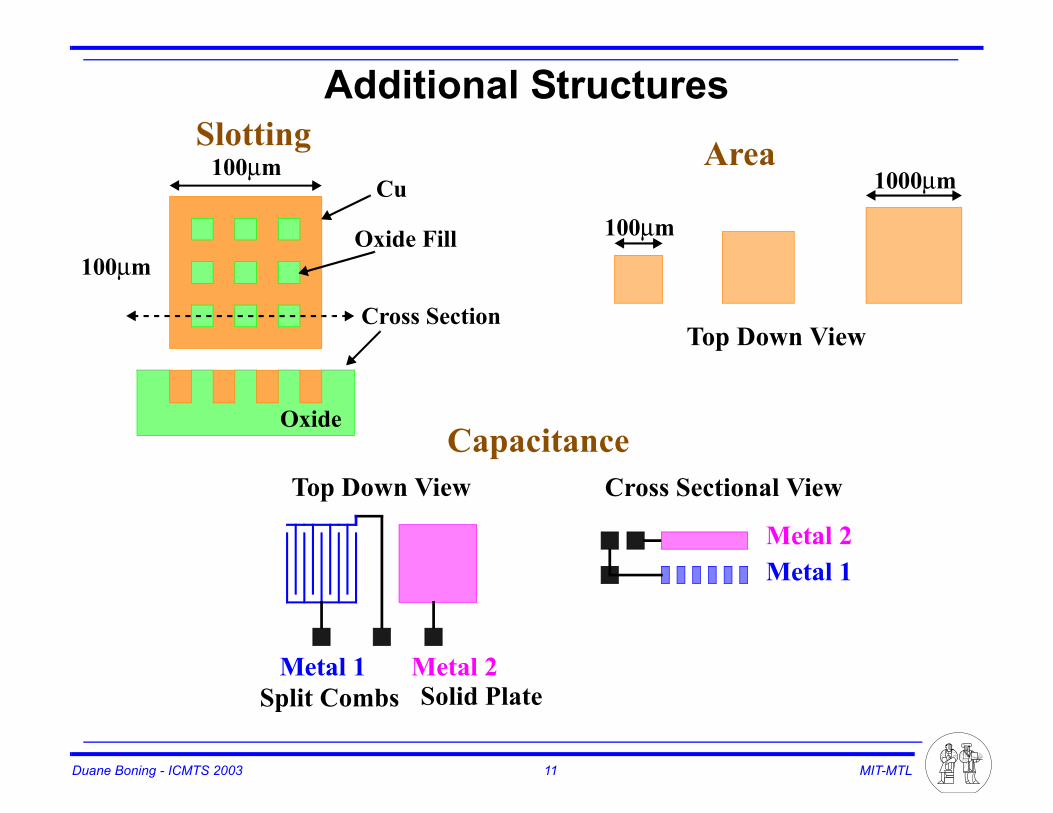
Additional Structures
Metal 1Metal 2
Top Down View Cross Sectional View
Split Combs Solid Plate
100µm
100µm
Cross Section
Oxide Fill
Cu
Oxide
Slotting
Capacitance
Area
Top Down View
100µm
1000µm
Metal 2Metal 1
Duane Boning - ICMTS 2003 12 MIT-MTL
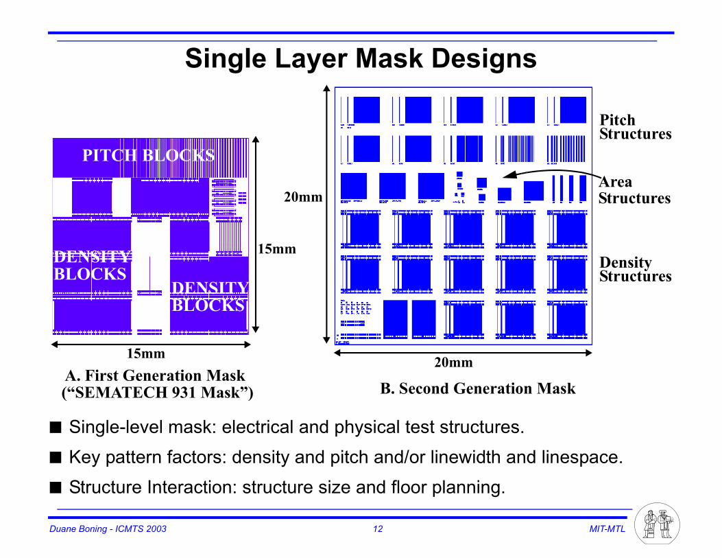
Single Layer Mask Designs
■ Single-level mask: electrical and physical test structures.■ Key pattern factors: density and pitch and/or linewidth and linespace.■ Structure Interaction: structure size and floor planning.
PITCH BLOCKS
DENSITYBLOCKS
DENSITYBLOCKS
15mm
15mmA. First Generation Mask(“SEMATECH 931 Mask”) B. Second Generation Mask
20mm
20mm
PitchStructures
DensityStructures
AreaStructures
Duane Boning - ICMTS 2003 13 MIT-MTL
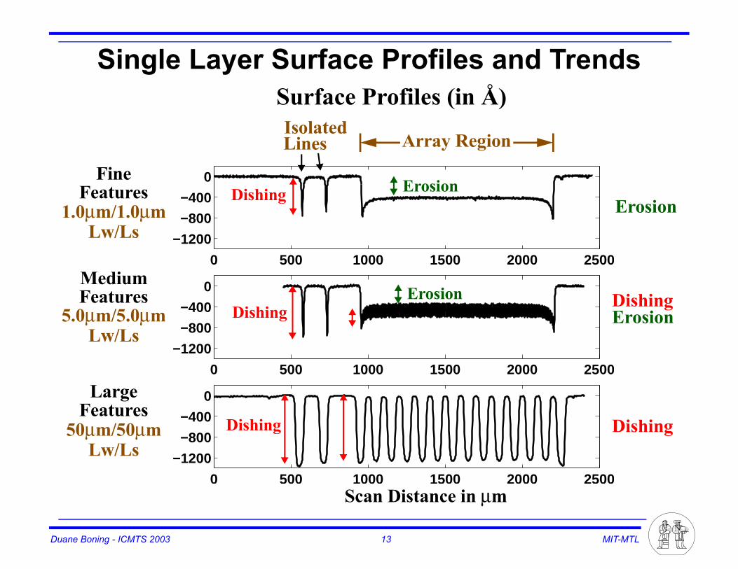
Single Layer Surface Profiles and Trends
0 500 1000 1500 2000 2500
−1200
−800
−400
0
0 500 1000 1500 2000 2500
−1200
−800
−400
0
0 500 1000 1500 2000 2500
−1200
−800
−400
0
5.0µm/5.0µm
50µm/50µm
1.0µm/1.0µm
Isolated
Scan Distance in µm
Surface Profiles (in Å)
Lines
ErosionDishing
Lw/Ls
Lw/Ls
Lw/Ls
ErosionErosion
DishingErosion
Dishing
Array Region
Dishing
Dishing
FineFeatures
MediumFeatures
LargeFeatures
Duane Boning - ICMTS 2003 14 MIT-MTL
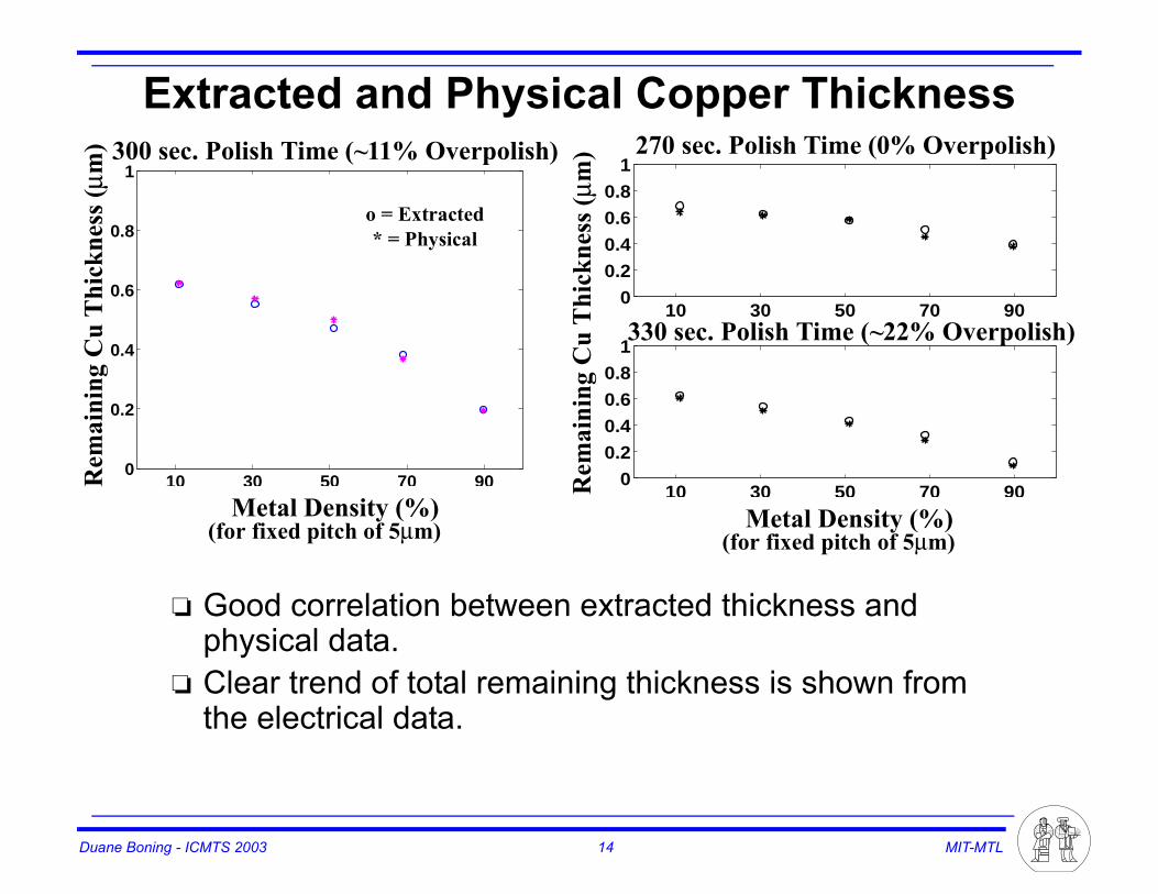
Extracted and Physical Copper Thickness
10 30 50 70 900
0.2
0.4
0.6
0.8
1
10 30 50 70 900
0.20.40.60.8
1
10 30 50 70 900
0.20.40.60.8
1
o = Extracted* = Physical
Metal Density (%)(for fixed pitch of 5µm)
Rem
aini
ng C
u T
hick
ness
(µm
) 300 sec. Polish Time (~11% Overpolish)
Metal Density (%)(for fixed pitch of 5µm)
Rem
aini
ng C
u T
hick
ness
(µm
) 270 sec. Polish Time (0% Overpolish)
330 sec. Polish Time (~22% Overpolish)
❏ Good correlation between extracted thickness and physical data.
❏ Clear trend of total remaining thickness is shown from the electrical data.
Duane Boning - ICMTS 2003 15 MIT-MTL
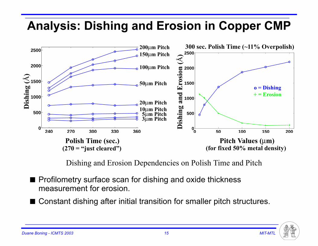
Analysis: Dishing and Erosion in Copper CMP
240 270 300 330 3600
500
1000
1500
2000
2500
0 50 100 150 2000
500
1000
1500
2000
2500
Dis
hing
(Å)
Polish Time (sec.)(270 = “just cleared”)
Dis
hing
and
Ero
sion
(Å)
o = Dishing+ = Erosion
Pitch Values (µm)(for fixed 50% metal density)
Dishing and Erosion Dependencies on Polish Time and Pitch
300 sec. Polish Time (~11% Overpolish)
5µm Pitch3µm Pitch
20µm Pitch
50µm Pitch
100µm Pitch
150µm Pitch200µm Pitch
10µm Pitch
■ Profilometry surface scan for dishing and oxide thicknessmeasurement for erosion.
■ Constant dishing after initial transition for smaller pitch structures.

Duane Boning - ICMTS 2003 16 MIT-MTL
Multilevel Process Sequence and Pattern Problems
Metal 1
Metal 2
Oxide
Oxide M1 Copper Lines
M2 Recess
M2 Remaining
As Dep.Oxide Profile
Oxide
Oxide
As Dep.Oxide Profile
ThicknessOxide
Metal 2
Oxide
Oxide
1. M1 Polish
2. M2 Oxide Deposition
3. M2 Cu Deposition
4. M2 Polish
Metal 1
Duane Boning - ICMTS 2003 17 MIT-MTL
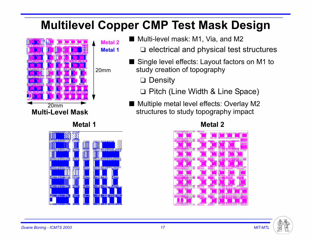
Multilevel Copper CMP Test Mask Design■ Multi-level mask: M1, Via, and M2
❑ electrical and physical test structures■ Single level effects: Layout factors on M1 to
study creation of topography❑ Density❑ Pitch (Line Width & Line Space)
■ Multiple metal level effects: Overlay M2 structures to study topography impact
20mm
20mm
Metal 1 Metal 2
Multi-Level Mask
Metal 2Metal 1
Duane Boning - ICMTS 2003 18 MIT-MTL
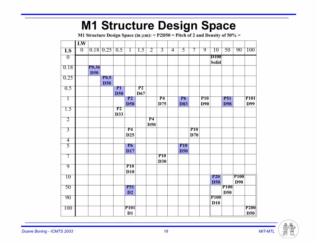
M1 Structure Design Space M1 Structure Design Space (in µm): < P2D50 = Pitch of 2 and Density of 50% >
LWLS 0 0.18 0.25 0.5 1 1.5 2 3 4 5 7 9 10 50 90 1000 D100
Solid0.18 P0.36
D500.25 P0.5
D500.5 P1
D50P2
D671 P2
D50P4
D75P6
D83P10D90
P51D98
P101D99
1.5 P2D33
2 P4D50
3 P4D25
P10D70
45 P6
D17P10D50
7 P10D30
9 P10D10
10 P20D50
P100D90
50 P51D2
P100D50
90 P100D10
100 P101D1
P200D50
Duane Boning - ICMTS 2003 19 MIT-MTL
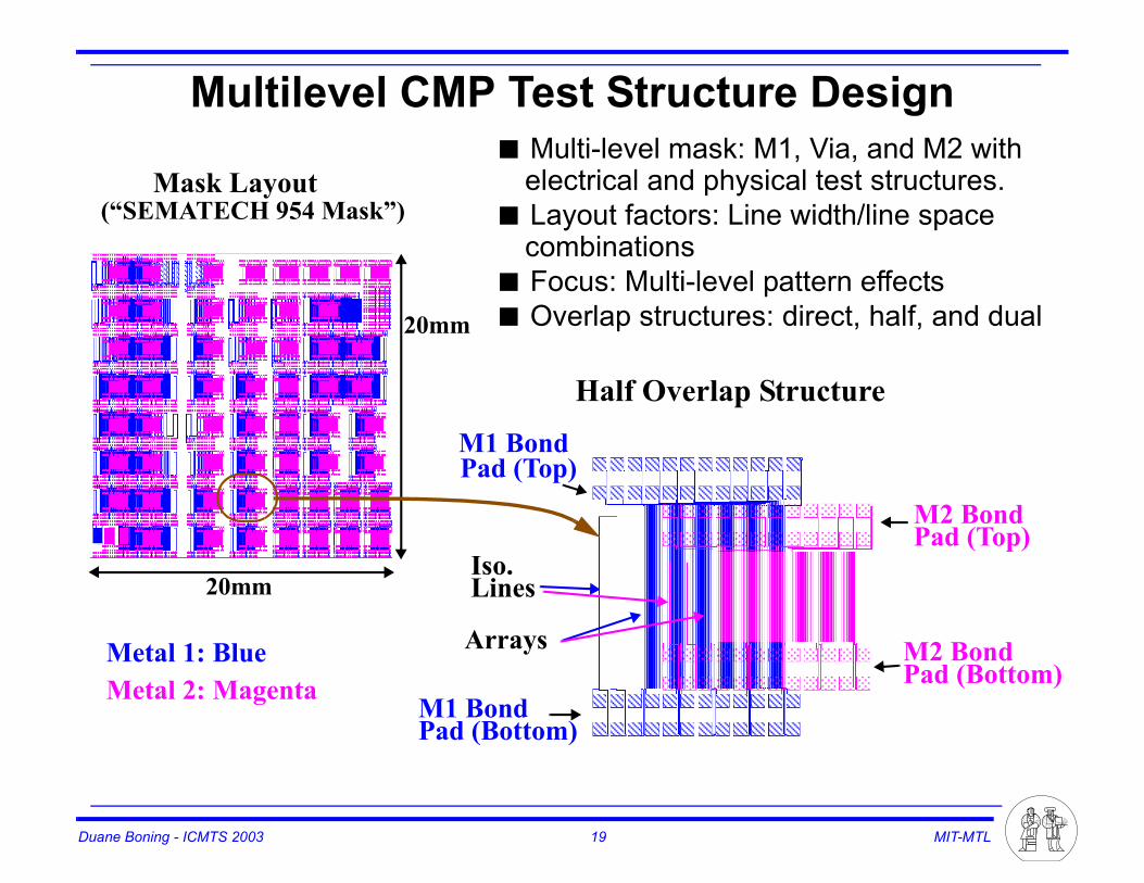
Multilevel CMP Test Structure Design
Half Overlap Structure
Mask Layout
20mm
20mm
Metal 1: BlueMetal 2: Magenta
Arrays M2 Bond
M2 Bond
M1 Bond
M1 Bond
Iso.Lines
Pad (Top)
Pad (Bottom)
Pad (Top)
Pad (Bottom)
(“SEMATECH 954 Mask”)
■ Multi-level mask: M1, Via, and M2 with electrical and physical test structures.
■ Layout factors: Line width/line space combinations
■ Focus: Multi-level pattern effects■ Overlap structures: direct, half, and dual
Duane Boning - ICMTS 2003 20 MIT-MTL
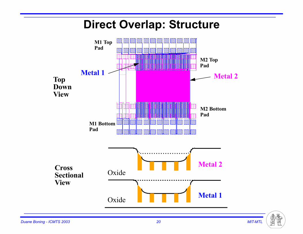
Direct Overlap: Structure
Metal 1 Metal 2
Oxide
Oxide
M1 BottomPad
M1 TopPad
M2 TopPad
M2 BottomPad
CrossSectionalView
TopDownView
Metal 2
Metal 1
Duane Boning - ICMTS 2003 21 MIT-MTL
Direct Overlap: Data Analysis
OxideAs Dep.Oxide Profile
Metal 2
Metal 1Oxide
0.5
0.6
0.7
0.8
−2000
−1000
0
−500 0 500 1000 1500 20000.5
0.6
0.7
0.8
M2
Rem
ain.
Thi
ck. (
µm)
M2
Rec
ess
M1
Rem
ain.
Thi
ck. (
µm)
µm
M2: Surface Scan
M2: Electrically Extracted
M1: Electrically Extracted
No Overlap
Overlap
Iso. Lines
Iso. Lines
(Å)

Duane Boning - ICMTS 2003 22 MIT-MTL
Multilevel Half Overlap Structure
As Dep.Oxide Profile
Metal 1 Metal 2
Oxide
Oxide
M1 BottomPad
M1 TopPad
M2 TopPad
M2 BottomPad
CrossSectionalView
TopDownView
Metal 2
Metal 1
Duane Boning - ICMTS 2003 23 MIT-MTL
Half Overlap: Erosion to Erosion
0.5
0.6
0.7
0.8
−2000
−1000
0
0 500 1000 1500 2000 25000.5
0.6
0.7
0.8
Iso. Lines
Over OverStruct. Oxide
M2: Electrically Extracted
M2: Surface Scan
M1: Electrically Extracted
µm
Ref.
Oxide
Oxide
As Dep.Oxide Profile
M2
Rem
ain.
Thi
ck. (
µm)
M2
Rec
ess
M1
Rem
ain.
Thi
ck. (
µm)
(Å)
Metal 2
Metal 1
Duane Boning - ICMTS 2003 24 MIT-MTL
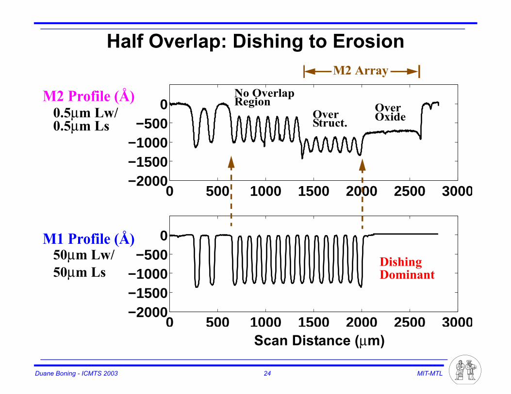
Half Overlap: Dishing to Erosion
0 500 1000 1500 2000 2500 3000−2000−1500−1000
−5000
0 500 1000 1500 2000 2500 3000−2000−1500−1000
−5000
M2 Profile (Å) No OverlapRegion Over
Oxide0.5µm Lw/ OverStruct.
M1 Profile (Å)
Scan Distance (µm)
0.5µm Ls
50µm Lw/50µm Ls
M2 Array
DishingDominant
Duane Boning - ICMTS 2003 25 MIT-MTL
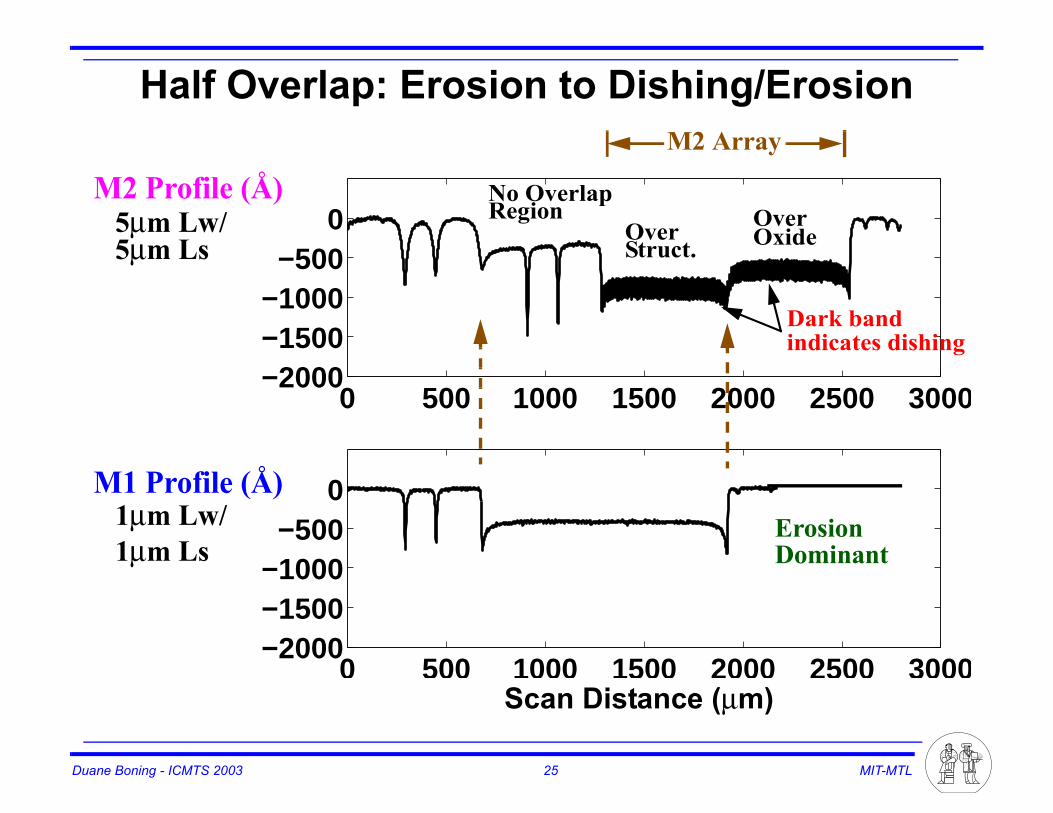
Half Overlap: Erosion to Dishing/Erosion
0 500 1000 1500 2000 2500 3000−2000−1500−1000
−5000
0 500 1000 1500 2000 2500 3000−2000−1500−1000
−5000
Dark bandindicates dishing
M2 Profile (Å) No OverlapRegion Over
Oxide5µm Lw/ OverStruct.
M1 Profile (Å)
Scan Distance (µm)
5µm Ls
1µm Lw/1µm Ls
M2 Array
ErosionDominant

Duane Boning - ICMTS 2003 26 MIT-MTL
Dual Overlap: Structure
Oxide
Oxide
As Dep.Oxide Profile
Metal 2
Metal 1
Metal 1
Metal 2
M1 BottomPad
M1 TopPad
M2 TopPad
M2 BottomPad
CrossSectionalView
TopDownView
Duane Boning - ICMTS 2003 27 MIT-MTL
Dual Overlap: Data Analysis
0.5
0.6
0.7
0.8
−2000
−1000
0
0 500 1000 1500 2000 2500 30000.5
0.6
0.7
0.8
OverStruct.1
M2 Electrically Extracted
Ref.
M2: Surface Scan
M1: Electrically Extracted
µm
OverStruct.2
Iso. Lines
Oxide
OxideMetal 2
Metal 1
M2
Rem
ain.
Thi
ck. (
µm)
M2
Rec
ess
M1
Rem
ain.
Thi
ck. (
µm)
(Å)
As Dep.Oxide Profile
Duane Boning - ICMTS 2003 28 MIT-MTL
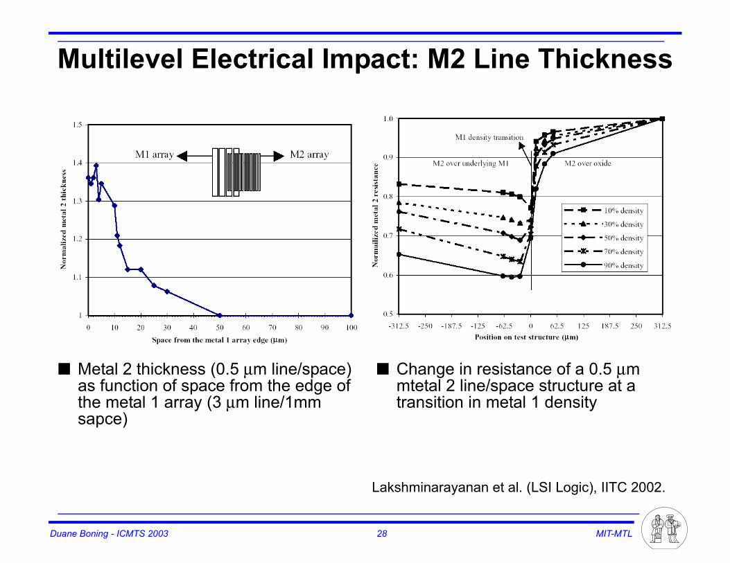
Multilevel Electrical Impact: M2 Line Thickness
■ Metal 2 thickness (0.5 µm line/space) as function of space from the edge of the metal 1 array (3 µm line/1mm sapce)
■ Change in resistance of a 0.5 µm mtetal 2 line/space structure at a transition in metal 1 density
Lakshminarayanan et al. (LSI Logic), IITC 2002.

Duane Boning - ICMTS 2003 29 MIT-MTL
Design Rule Generation
Lakshminarayanan et al. (LSI Logic), IITC 2002.
Duane Boning - ICMTS 2003 30 MIT-MTL
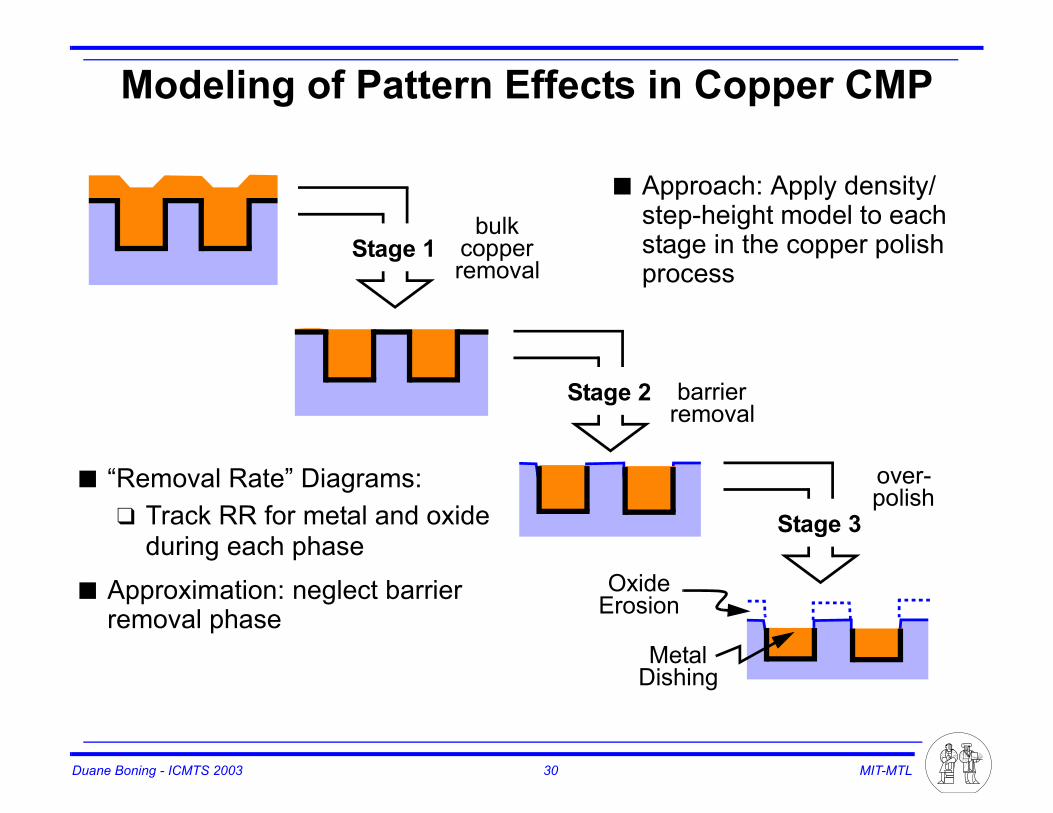
Modeling of Pattern Effects in Copper CMP
bulk
OxideErosion
MetalDishing
Stage 1 copperremoval
Stage 2 barrierremoval
Stage 3
over-polish
■ Approach: Apply density/step-height model to each stage in the copper polish process
■ “Removal Rate” Diagrams:❑ Track RR for metal and oxide
during each phase■ Approximation: neglect barrier
removal phase

Duane Boning - ICMTS 2003 31 MIT-MTL
Pattern-Density / Step-Height Effects
■ For large step heights: ❒ step height reduction goes as
1/pattern-density
■ For small step heights (less than the “contact height”): ❒ height reduction proportional
to height❒ height decays with time constant τ:
H t( ) H0e t τ⁄–=
H
tdd H t( ) 1
τ---H t( )–=
tdd H t( ) K
ρ----–=td
dH
Step HeightHc
Wafer
Wafer
CMP Pad
CMP Pad
Hc
X
PL
■ Calculate effective density by averaging local pattern densities over some window/weighting function
EffectiveDensity MapOver Chip
Ouma et al., IITC ‘98;Smith et al., CMPMIC ‘99Grillaert et al., CMP-MIC ‘98.

Duane Boning - ICMTS 2003 32 MIT-MTL
Chip-Scale CMP Simulation
0
500
1000
1500
2000
Cu Dishing after step 2 polish
50 100 150 200 250 300 350 400 450 500
100
200
300
400
500
600
700
Dishing after step two
RMS Error = 155 Å
Å
0 5 10 15 20 25 30 35 40 450
50
100
150
200
250
300
Site number
Dis
hin
g (
A)
Data Model
Site number
Dis
hing
(Å)
Duane Boning - ICMTS 2003 33 MIT-MTL
Outline■ Background
■ Copper CMP Characterization
■ Copper Electroplating Characterization❏ Definitions❏ Test Structure and Measurement Plan❏ Trend Analysis❏ Chip Scale Modeling❏ Integrated Plating/CMP Chip-Scale Modeling
■ Conclusions

Duane Boning - ICMTS 2003 34 MIT-MTL
Copper Electroplating Non-UniformitiesIsolatedLine
Array Region
Conventional Fill Super Fill(Bottom-Up Fill)
■ Isolated line and array region are recessed
■ Isolated line sticks up and array region is bulged

Duane Boning - ICMTS 2003 35 MIT-MTL
Electroplating Pattern Dependent Effects
0
Sample Profilometer
Oxide
SH
AH
0
Fine Line Large Line Fine Line Large LineFine Space Large Space Medium Space Fine Space
AH
AH
SH
AH: Array Height SH: Step Height
SH
AH
Scans
Duane Boning - ICMTS 2003 36 MIT-MTL
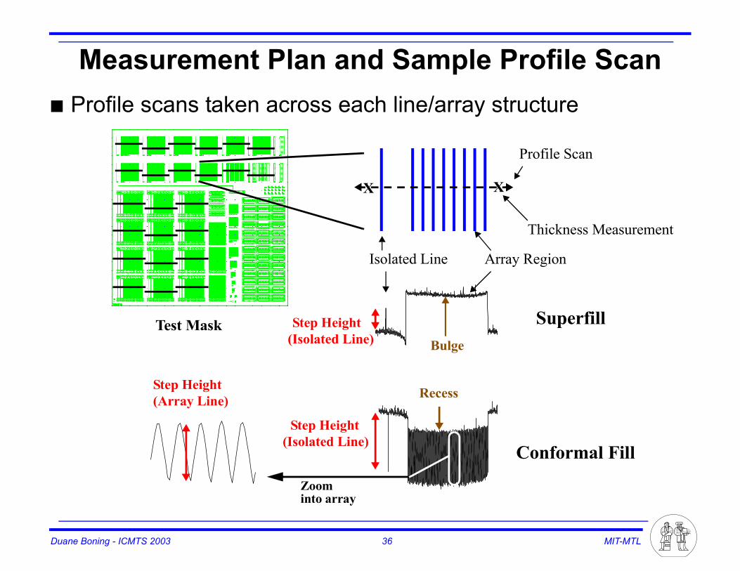
Measurement Plan and Sample Profile Scan■ Profile scans taken across each line/array structure
Isolated Line Array Region
Thickness Measurement
Bulge
Zoom
Recess
Step Height
Step Height
Step Height(Isolated Line)
(Isolated Line)
(Array Line)
into array
Superfill
Conformal Fill
Test Mask
X X
Profile Scan

Duane Boning - ICMTS 2003 37 MIT-MTL
Electroplated Profile Trends: Pitch Structures
0 1000 2000 3000
−5000
0
5000
2um/2um
0 1000 2000 3000
−5000
0
5000
5um/5um
0 1000 2000 3000
−5000
0
5000
10um/10um
0 1000 2000 3000
−5000
0
5000
20um/20um
0 1000 2000 3000
−5000
0
5000
50um/50um
0 1000 2000 3000
−5000
0
5000
100um/100um
0 1000 2000 3000
−5000
0
5000
0.25um/0.25um
0 1000 2000 3000
−5000
0
5000
0.3um/0.3um
0 1000 2000 3000
−5000
0
5000
0.35um/0.35um
0 1000 2000 3000
−5000
0
5000
0.5um/0.5um
0 1000 2000 3000
−5000
0
5000
0.7um/0.7um
0 1000 2000 3000
−5000
0
5000
1um/1um
Hei
ght (
Å)
Trace Length (µm)
Lw/Ls
Hei
ght (
Å)
0.25/0.25µm 0.35/0.35µm0.3/0.3µm
0.5/0.5µm 1/1µm0.7/0.7µm
2/2µm 10/10µm5/5µm
20/20µm 100/100µm50/50µm
Superfill
ConformalBehavior
Behavior
Duane Boning - ICMTS 2003 38 MIT-MTL
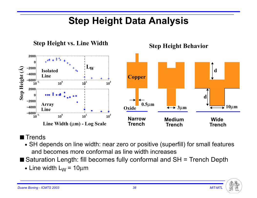
Step Height Data Analysis
10−1
100
101
102
−6000
−4000
−2000
0
2000
10−1
100
101
102
−6000
−4000
−2000
0
2000
Line Width (µm) - Log Scale
ArrayLine
IsolatedLine
LW
Step
Hei
ght (
Å)
Step Height vs. Line Width
■ Trends• SH depends on line width: near zero or positive (superfill) for small features
and becomes more conformal as line width increases■ Saturation Length: fill becomes fully conformal and SH = Trench Depth• Line width LW
= 10µm
0.5µm
Copper
Oxide 3µm 10µm
d
d
NarrowTrench
WideTrench
MediumTrench
Step Height Behavior
Duane Boning - ICMTS 2003 39 MIT-MTL
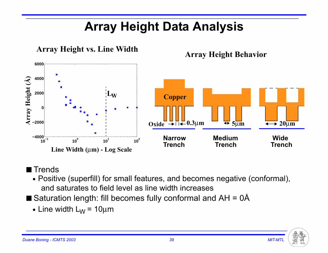
Array Height Data Analysis
10−1
100
101
102
−4000
−2000
0
2000
4000
6000
■ Trends• Positive (superfill) for small features, and becomes negative (conformal),
and saturates to field level as line width increases■ Saturation length: fill becomes fully conformal and AH = 0Å• Line width LW
= 10µm
Line Width (µm) - Log Scale
LW
Arr
ay H
eigh
t (Å
)
Array Height vs. Line Width
0.3µm 5µm 20µmOxide
NarrowTrench
WideTrench
MediumTrench
Array Height Behavior
Copper

Duane Boning - ICMTS 2003 40 MIT-MTL
SH and AH vs. Line Space
■ Trends• Line space dependency for SH and AH is similar to line width dependency
■ Saturation length: similar value is observed for line space• Line space LS = 10µm
Array Height vs. Line Space
10−1
100
101
102
−4000
−2000
0
2000
4000
6000
Arr
ay H
eigh
t (Å
)
LS
10−1
100
101
102
−6000
−5000
−4000
−3000
−2000
−1000
0
1000
2000
LS
Step
Hei
ght (
Å)
Step Height vs. Line Space
ArrayLine
Line Space (µm) - Log ScaleLine Space (µm) - Log Scale

Duane Boning - ICMTS 2003 41 MIT-MTL
Transition Length Scale in Electroplating■ Plating depends on local feature (feature scale) and nearest
neighbors within 2-5µm range
720 730 740 750 760 770 780−1000
0
1000
2000
2720 2730 2740 2750 2760 2770 2780−1000
0
1000
2000
700 750 800 850−4000
−3000
−2000
−1000
0
2650 2700 2750 2800−4000
−3000
−2000
−1000
0
Arr
ay H
eigh
t (Å
)
Array Height Profile Scans
Right Edge
Left Edge
~5µm
~5µm
Right Edge
Left Edge
Scan Length (µm) Scan Length (µm)
Arr
ay H
eigh
t (Å
)
Superfill Conventional fill
0.5µm/0.5µm Array 5µm/5µm Array
Sharp Transition
4.5µm/0.5µm Array
1.5µm/3.5µm Array
Array to ArrayTransition
Duane Boning - ICMTS 2003 42 MIT-MTL
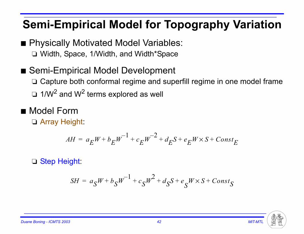
Semi-Empirical Model for Topography Variation■ Physically Motivated Model Variables:
❏ Width, Space, 1/Width, and Width*Space
■ Semi-Empirical Model Development❏ Capture both conformal regime and superfill regime in one model frame
❏ 1/W2 and W2 terms explored as well
■ Model Form❏ Array Height:
❏ Step Height:
AH aEW bEW 1– cEW 2– dES eEW S× ConstE+ + + + +=
SH aSW bSW 1– cSW2 dSS e+S
W S× ConstS+ + + +=
Duane Boning - ICMTS 2003 43 MIT-MTL
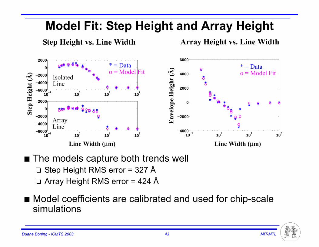
Model Fit: Step Height and Array Height
10−1
100
101
102
−6000
−4000
−2000
0
2000
10−1
100
101
102
−6000
−4000
−2000
0
2000
Line Width (µm)
ArrayLine
IsolatedLine
Step
Hei
ght (
Å)
Step Height vs. Line Width
* = Datao = Model Fit
10−1
100
101
102
−4000
−2000
0
2000
4000
6000
Line Width (µm)
Env
elop
e H
eigh
t (Å
)
Array Height vs. Line Width
* = Datao = Model Fit
■ The models capture both trends well❏ Step Height RMS error = 327 Å❏ Array Height RMS error = 424 Å
■ Model coefficients are calibrated and used for chip-scale simulations

Duane Boning - ICMTS 2003 44 MIT-MTL
Chip-Scale Simulation Calibration Results
■ Simulated over the entire test mask used to calibrate the model■ RMS errors are slightly greater (about 90Å and 10Å more) than fitting RMS
errors since distribution values are used
1
1.2
1.4
1.6
1.8
2
2.2
x 104Final Thickness Average: Simulated Result
50 100 150 200 250 300 350 400 450 500
50
100
150
200
250
300
350
400
450
500
0
500
1000
1500
2000
2500
3000
3500
4000
4500
5000
Step Height Average: Simulated Result
50 100 150 200 250 300 350 400 450 500
50
100
150
200
250
300
350
400
450
500
−4000
−2000
0
2000
4000
6000
Envelope Average: Simulated Result
50 100 150 200 250 300 350 400 450 500
50
100
150
200
250
300
350
400
450
500
Array
Step
Final
Test
Thickness
HeightMask
RMS Error=440Å
RMS Error=420Å
Height

Duane Boning - ICMTS 2003 45 MIT-MTL
Integration of Electroplating and CMP Models■ Integration is done by feeding forward the simulated result
from electroplating to copper CMP simulation
■ Electroplating Simulation:• Array Height• Step Height• Topography Pattern Density
Prediction of dishing and erosion
Calibrated Copper Pattern Dependent
CMP ModelChip-Scale Simulation
Layout ParameterExtraction
Product Chip
Oxide
CopperLayout
Surface Envelope
■ CMP model needs:❏ Surface “envelope”:
Array Height❏ Step Height❏ Topography Pattern
Density
Duane Boning - ICMTS 2003 46 MIT-MTL
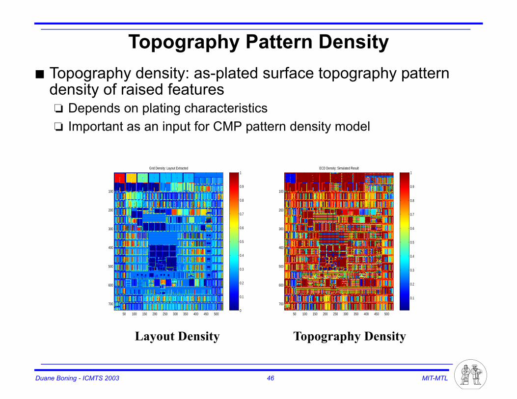
Topography Pattern Density■ Topography density: as-plated surface topography pattern
density of raised features❏ Depends on plating characteristics❏ Important as an input for CMP pattern density model
Topography DensityLayout Density
0
0.1
0.2
0.3
0.4
0.5
0.6
0.7
0.8
0.9
1Grid Density: Layout Extracted
50 100 150 200 250 300 350 400 450 500
100
200
300
400
500
600
700
0.1
0.2
0.3
0.4
0.5
0.6
0.7
0.8
0.9
1ECD Density: Simulated Result
50 100 150 200 250 300 350 400 450 500
100
200
300
400
500
600
700
Duane Boning - ICMTS 2003 47 MIT-MTL
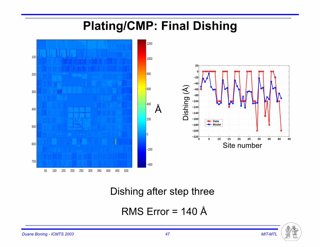
Plating/CMP: Final Dishing
−400
−200
0
200
400
600
800
1000
1200
Dishing after step 3 polish
50 100 150 200 250 300 350 400 450 500
100
200
300
400
500
600
700
Dishing after step three
RMS Error = 140 Å
Å
0 5 10 15 20 25 30 35 40 45−220
−200
−180
−160
−140
−120
−100
−80
−60
−40
−20
0
20
Site number
Dis
hin
g (
A)
Data Model
Site number
Dis
hing
(Å)
Duane Boning - ICMTS 2003 48 MIT-MTL
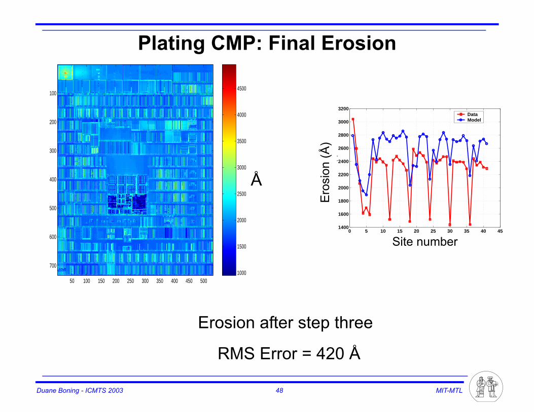
Plating CMP: Final Erosion
1000
1500
2000
2500
3000
3500
4000
4500
Erosion after step 3 polish
50 100 150 200 250 300 350 400 450 500
100
200
300
400
500
600
700
Erosion after step three
RMS Error = 420 Å
Å
0 5 10 15 20 25 30 35 40 451400
1600
1800
2000
2200
2400
2600
2800
3000
3200
Site number
Ero
sio
n (
A)
Data Model
Site number
Ero
sion
(Å)
Duane Boning - ICMTS 2003 49 MIT-MTL
Conclusion■ Electroplating and CMP are Highly Pattern Dependent
■ Copper Interconnect Pattern Dependent Characterization❏ Test Structure Design
• Capture Key Pattern Effects: Isolated vs. Array, Density, Pitch, etc.• Three Polishing Length Scales: mm, 100µm, and 1µm Ranges.
❏ Mask Design• Single layer• Multi layer
❏ Physical and Electrical Measurements❏ Data Analysis
■ Can Be Applied to Support Process Development, Optimization, and Formulation Of Design Rules
■ Provides Data for Chip-Scale Modeling of Copper Interconnect

Duane Boning - ICMTS 2003 50 MIT-MTL
Acknowledgments■ Past and current students: Tae Park, Tamba Tugbawa, Brian
Lee, Xiaolin Xie, Hong Cai
■ Support and collaboration with SEMATECH, Texas Instruments, Conexant, Praesagus, SKW, Philips Analytical


