Download - NOR THWESTERN UNIVERSITY Gro Si/Ge

NORTHWESTERN UNIVERSITY
Growth and Characterization of Si/Ge
Heterostructures on Si(001) Surface and Ge
Nano{Dots on Patterned Si(001) Surface
A DISSERTATION
SUBMITTED TO THE GRADUATE SCHOOL
IN PARTIAL FULFILLMENT OF THE REQUIREMENTS
for the degree
DOCTOR OF PHILOSOPHY
Field of Physics and Astronomy
By
William Pascal Rodrigues
EVANSTON, ILLINOIS
December 2000

c Copyright by William Pascal Rodrigues 2000
All Rights Reserved
ii

ABSTRACT
Growth and Characterization of Si/Ge/ Heterostructures
on Si(001) Surface and Ge Nano{dots on Patterned
Si(001) Surface
William Pascal Rodrigues
The epitaxial growth of Si/Ge heterostructures on the Si(001) surface has been
the subject of much research because of its interesting properties and technological
applications. Scienti�cally Ge/Si(001) is interesting because it is an ideal system
to study strained heteroepitaxy. Such strained heteroepitaxial layers of Si/Ge on
Si(001) can have superior device performance compared to Si based devices.
In this thesis, using x{ray synchrotron radiation, we have performed structural
studies of Si/Ge heterostructures grown on Si(001) by surfactant mediated epitaxy
with Bi as the surfactant. High resolution measurements were performed using
the x{ray standing wave technique to characterize the structure of atomic layers in
ultra{thin Ge �lms on Si(001). Our results indicate that the Ge atomic layers are
highly commensurate with the Si substrate lattice in the in{plane direction but less
so in the surface normal direction. Using grazing incidence x{ray di�raction we
measured the critical thickness for pseudomorphic growth of Ge on Si(001) with Bi
as surfactant to be 7 monolayers (ML). In comparison with Ge growth without Bi,
segregation of Ge in the Si cap layer was suppressed and the Ge �lm was partially
relaxed at 10 ML. Using x{ray specular re ectivity we measured the Ge{Si cap
interface roughness and found it to be signi�cantly larger for Ge �lm thicknesses
above 7 ML.
We also investigated the morphology of Ge nano{dots grown by molecular
beam epitaxy on lithographically patterned Si(001) stripe{mesas. Our atomic force
iii

microscopy (AFM) images for Ge grown on stripe{mesas show increased uniformity
in Ge nano{dot size, shape, and orientation compared with Ge nano{dots grown
on a planar Si(001) surface. On stripe{mesas we also observed preferential growth
of Ge nano{dots along the edges of the stripe{mesas.
iv

Acknowledgments
I would like to thank my advisor Prof. Michael Bedzyk for his constant encour-
agement, guidance and support. This thesis work would not have been possible
without the generous �nancial support from Argonne National Laboratory and for
that I am grateful to Dr. Wenbing Yun and Dr. Barry Lai. Wenbing Yun and
Michael Bedzyk introduced me to the Advanced Photon Source at ANL.
At Northwestern University I would like to thank all my coworkers especially
Tien{Lin Lee and Osami Sakata for all their help and advice. I am also thank-
ful to Prof. John Ketterson and his group for introducing me to electron{beam
lithography and photolithography and for the free use of those facilities in their
lab.
At ANL I would like to thank the SR1{2 sta� members, postdoctoral fellows,
technicians and outside users, in particular Wenbing Yun, Barry Lai, Zhonghou
Cai, and Peter Ilinski, for introducing me to the new and exciting �eld of x{ray
microscopy. I am also thankful to Derrick Mancini and Yong Chu for their advice
and Joseph Arko for all his valuable help. I would also like to thank Peter Baldo
from MSD{ANL for performing the RBS measurements.
I am thankful to all my friends at Northwestern for making my stay very
pleasurable and memorable one. Finally I am very grateful to my family for their
support. I dedicate this thesis to my parents.
v

Dedicated to my parents
Ursula and Pascal Ludrick
vi

Contents
Abstract iii
Acknowledgments v
1 Introduction 1
2 Brief Overview of Ge/Si(001) 4
2.1 Introduction . . . . . . . . . . . . . . . . . . . . . . . . . . . . . . . 4
2.2 Epitaxial Growth Modes . . . . . . . . . . . . . . . . . . . . . . . . 4
2.3 Epitaxial growth of Ge on Si(001) . . . . . . . . . . . . . . . . . . . 6
2.4 Epitaxial Growth of Si on Ge . . . . . . . . . . . . . . . . . . . . . 8
2.5 Surfactant Mediated Epitaxy . . . . . . . . . . . . . . . . . . . . . 8
3 Experimental Techniques 11
3.1 Introduction . . . . . . . . . . . . . . . . . . . . . . . . . . . . . . . 11
3.2 XSW Technique . . . . . . . . . . . . . . . . . . . . . . . . . . . . 11
3.2.1 XSW Experimental Setup . . . . . . . . . . . . . . . . . . . 18
3.3 GIXD . . . . . . . . . . . . . . . . . . . . . . . . . . . . . . . . . . 22
3.4 X{ray Specular Re ectivity . . . . . . . . . . . . . . . . . . . . . . 24
3.4.1 Experimental Setup for GIXD and x{ray re ectivity mea-surements . . . . . . . . . . . . . . . . . . . . . . . . . . . . 26
4 Sample Preparation and Standard Characterization 28
vii

4.1 Preparation of Si Substrates for X{ray Experiments . . . . . . . . . 28
4.2 Preparation of Lithographically Patterned Si Surfaces . . . . . . . . 29
4.2.1 Photolithography . . . . . . . . . . . . . . . . . . . . . . . . 30
4.2.2 E{beam Lithography . . . . . . . . . . . . . . . . . . . . . . 31
4.2.3 Etching . . . . . . . . . . . . . . . . . . . . . . . . . . . . . 33
4.3 UHV Chamber and MBE Growth . . . . . . . . . . . . . . . . . . . 34
4.3.1 MBE Surface Science Chamber . . . . . . . . . . . . . . . . 34
4.3.2 MBE growth . . . . . . . . . . . . . . . . . . . . . . . . . . 39
4.4 In situ LEED and AES Studies . . . . . . . . . . . . . . . . . . . . 40
4.4.1 Clean Si(001) surface . . . . . . . . . . . . . . . . . . . . . . 40
4.4.2 Bi terminated Si(001) surface . . . . . . . . . . . . . . . . . 42
4.5 Ge Coverage Calibration . . . . . . . . . . . . . . . . . . . . . . . . 44
5 X{ray Scattering Studies 49
5.1 Introduction . . . . . . . . . . . . . . . . . . . . . . . . . . . . . . . 49
5.2 Previous GIXD Studies . . . . . . . . . . . . . . . . . . . . . . . . . 50
5.3 GIXD and Re ectivity Results . . . . . . . . . . . . . . . . . . . . . 51
6 X-ray Standing Wave Studies 62
6.1 Introduction . . . . . . . . . . . . . . . . . . . . . . . . . . . . . . . 62
6.2 Structural models . . . . . . . . . . . . . . . . . . . . . . . . . . . . 63
6.2.1 Fixed bond length model . . . . . . . . . . . . . . . . . . . . 64
6.2.2 Strained Ge layer model based on elasticity theory . . . . . . 65
6.2.3 Relaxed Ge layer Model . . . . . . . . . . . . . . . . . . . . 66
6.3 XSW Results and Discussions for Ge . . . . . . . . . . . . . . . . . 66
6.3.1 Model 1 for Static Debye{Waller Factor . . . . . . . . . . . 80
6.3.2 Model 2 . . . . . . . . . . . . . . . . . . . . . . . . . . . . . 81
6.3.3 E�ect of surfactant . . . . . . . . . . . . . . . . . . . . . . . 87
6.3.4 XSW (008) Measurement . . . . . . . . . . . . . . . . . . . . 89
viii

6.4 XSW Results of Si Cap . . . . . . . . . . . . . . . . . . . . . . . . . 90
6.4.1 X-ray evanescent wave e�ect . . . . . . . . . . . . . . . . . . 90
7 Ge Growth on Patterned Si(001) 98
7.1 Introduction . . . . . . . . . . . . . . . . . . . . . . . . . . . . . . . 98
7.2 Electronic properties . . . . . . . . . . . . . . . . . . . . . . . . . . 98
7.3 Self assembled Ge island growth on Si(001) . . . . . . . . . . . . . . 99
7.3.1 Island distribution . . . . . . . . . . . . . . . . . . . . . . . 99
7.3.2 Lateral ordering . . . . . . . . . . . . . . . . . . . . . . . . . 101
7.3.3 Vertical ordering . . . . . . . . . . . . . . . . . . . . . . . . 103
7.4 Growth of Ge on patterned Si(001) . . . . . . . . . . . . . . . . . . 105
7.4.1 Growth on stripe{mesas . . . . . . . . . . . . . . . . . . . . 107
7.4.2 Growth on square{mesas . . . . . . . . . . . . . . . . . . . . 108
7.5 In situ LEED Studies . . . . . . . . . . . . . . . . . . . . . . . . . . 110
7.5.1 Coverage dependence . . . . . . . . . . . . . . . . . . . . . . 110
7.5.2 Temperature dependence . . . . . . . . . . . . . . . . . . . . 112
7.6 Morphology Studies . . . . . . . . . . . . . . . . . . . . . . . . . . . 115
8 Summary 123
8.1 Thesis Summary . . . . . . . . . . . . . . . . . . . . . . . . . . . . 123
8.2 Future Work . . . . . . . . . . . . . . . . . . . . . . . . . . . . . . . 125
References 126
Appendices 133
A Shiraki Etch for Si 134
A.1 CP4 Etch . . . . . . . . . . . . . . . . . . . . . . . . . . . . . . . . 134
A.2 Shiraki Etch . . . . . . . . . . . . . . . . . . . . . . . . . . . . . . . 134
B MBE Control System 136
ix

List of Tables
1 Measured coverages of Ge for all the samples. �No Bi was used forthis sample. . . . . . . . . . . . . . . . . . . . . . . . . . . . . . . . 47
2 Results of (004) and (022) XSW measurements for the Ge for allsamples . . . . . . . . . . . . . . . . . . . . . . . . . . . . . . . . . 68
3 Results of (004) XSW measurements for the Si cap.a Measured val-ues, b from continuum elasticity theory and c based on measured GeP004 values. . . . . . . . . . . . . . . . . . . . . . . . . . . . . . . . 97
x

List of Figures
1 Growth modes in epitaxy: Frank{van der Merwe (FM), Volmer{Weber (VW) and Stranski{Krastanov (SK). . . . . . . . . . . . . . 5
2 After Mo et al [18]. STM images of single \hut" cluster. (a) Per-spective plot. Scan area 400�A � 400�A. (b) Curvature mode greyscale plot. The inclined surfaces are f105g facets. . . . . . . . . . . 7
3 Schematic of XSW technique using Bragg re ection from perfectcrystals. The period of the XSW �eld is equal to the d{spacing forthe di�raction planes. . . . . . . . . . . . . . . . . . . . . . . . . . . 12
4 From reference [54]. (a) the real and imaginary part of the E{�eldratio EH=E0 as a function of the relative Bragg angle. (b) the phasev of the E{�eld ratio. (For the symmetric Si(004) re ection at thephoton energy of 12 keV). The above is for the origin de�ned in�gure 5 for the Si unit cell. . . . . . . . . . . . . . . . . . . . . . . . 15
5 The unit cell for bulk Si. The cubic unit cell has 8 Si atoms. Thecoherent position PH are measured with respect to the origin placedat the center of symmetry as shown. . . . . . . . . . . . . . . . . . 17
6 Side{view (except for the Ge uorescent detector) schematic of theXSW setup at the 5IDC station at APS. The L{N2 cooled Si(111)monochromator is 30 m from the undulator. The other componentsstarting with ion chamber IC1 sitting on a optical table in the frontend of the 5ID-C hutch are approximately 55 m from the undulator. 19
7 DuMond diagram (a) for the x{ray optics used for XSW measure-ments, (b) for Si(004) re ection and (c) for Si(022) re ection. X{axisis the incident angle in �rad and Y{axis is the wavelength. . . . . . 20
8 Schematic diagram for GIXD. In our GIXD experiments �i = �f . . 23
9 Schematic diagram for x{ray specular re ectivity. � > �c. . . . . . 24
xi

10 Schematic of experimental setup for GIXD and x{ray re ectivity atAPS. . . . . . . . . . . . . . . . . . . . . . . . . . . . . . . . . . . . 27
11 Partial pressures for residual gases inside the chamber under UHVconditions. The H2 partial pressure is 2� 10�10 torr. . . . . . . . . 35
12 Schematic side{view of the MBE chamber. All the essential portsare shown. The LEED port is out of the plane of the paper whilethe STM port is diametrically opposite to the LEED. . . . . . . . . 36
13 An isometric view of the manipulator head. The manipulator ismachined out of Mo. The two sample holder plates for direct andindirect sample heating are also shown. . . . . . . . . . . . . . . . . 38
14 2{domain 2� 1 LEED pattern of clean Si(001) surface. . . . . . . . 41
15 Auger spectrums for clean and unclean Si(001) surfaces. Note thatfor clean surface the sensitivity was increased by a factor of 10 forE > 130 eV. . . . . . . . . . . . . . . . . . . . . . . . . . . . . . . . 42
16 Bi(NOO)/Si(LMM) Auger intensity ratio as a function of substratetemperature. Bi coverage beyond 400ÆC decreases linearly with tem-perature. . . . . . . . . . . . . . . . . . . . . . . . . . . . . . . . . . 44
17 (a) 2{domain 2�n LEED pattern for Bi terminated Si(001) surface,resulting from missing Bi dimer as shown in (b). Atoms in thesecond layer form a dimer at that site. With n � 5, the coveragesis estimated to be 1� 1=n about 0.8 ML. . . . . . . . . . . . . . . . 45
18 Atomic view of Si/Ge growth on Si(001) with Bi as the surfactant.(a) Bi dimers on Si(001) surface after 1ML Bi coverage. (b) afterGe deposition on Bi covered surface, and (c) after Si deposition fol-lowing Ge growth. Driven by the surface free energy minimization,Bi segregates to the growth surface and forms a Bi{Bi dimer at eachstage. . . . . . . . . . . . . . . . . . . . . . . . . . . . . . . . . . . . 46
19 Calibration of Ge coverage by exciting Ge K� uorescence. Solidlines are Gaussian �ts to the data (points). The Ge coverage isproportional to the area under the peak. . . . . . . . . . . . . . . . 48
20 Scattering depth � for 11 keV x{rays as function of L. The incidentand exit angles are equal. . . . . . . . . . . . . . . . . . . . . . . . . 52
xii

21 H;K scans through (22L) with L = 0:01 for Si/Ge layers with a)10.0 ML of Ge grown with Bi and b) 10.0 ML of Ge grown withoutBi. The scans are shifted vertically for clarity. The inset representsthe scanning in reciprocal space. . . . . . . . . . . . . . . . . . . . . 54
22 H;K scans through (22L), with L = 0:04 for a) 10.0 ML Ge withoutBi, b) 10.0 ML Ge with Bi, c) 7.1 ML Ge with BI and d) 1.7 MLGe with Bi. . . . . . . . . . . . . . . . . . . . . . . . . . . . . . . . 55
23 H;K scans through (22L), with various values of L for sample with10.0 ML of Ge coverage grown with Bi. The scans are shifted ver-tically for clarity. . . . . . . . . . . . . . . . . . . . . . . . . . . . . 56
24 X{ray re ectivity data (points) and model �ts (lines) for a) 7.1 MLGe grown with Bi b) 10.0 ML of Ge grown with Bi. For 10 ML ofGe without Bi only the data is shown. . . . . . . . . . . . . . . . . 58
25 Scattering depth � for 11 keV x{rays as function of L. The incidentand exit angles are equal. . . . . . . . . . . . . . . . . . . . . . . . . 59
26 Positions of various Ge layers above the Si substrate. The bulkSi(004) di�raction planes, where P004 = 0, are represented by thedashed lines. . . . . . . . . . . . . . . . . . . . . . . . . . . . . . . . 64
27 Two structural models for Ge epitaxial growth on Si; (a) bondlengths conserved, (b) continuum elasticity theory model. . . . . . . 65
28 Calculated coherent position of Ge for (a) �xed bond length model,(b) elastic model (c) relaxed Ge model as a function of coverage. . . 67
29 Angular dependence of (004) (top) and (022) (bottom) XSW dataand best �t (solid lines) for normalized Ge K� and uorescence yieldand re ectivity for 1.6 ML Ge grown with Bi on Si(001). . . . . . . 69
30 Angular dependence of (004) (top) and (022) (bottom) XSW dataand best �t (solid lines) for normalized Ge K� and uorescence yieldand re ectivity for 1.1 ML Ge grown on Si(001). . . . . . . . . . . . 70
31 Angular dependence of (004) (top) and (022) (bottom) XSW dataand best �t (solid lines) for normalized Ge K� and uorescence yieldand re ectivity for 3.4 ML Ge grown with on Si(001). . . . . . . . . 71
32 Angular dependence of (004) (top) and (022) (bottom) XSW dataand best �t (solid lines) for normalized Ge K� and uorescence yieldand re ectivity for 3.0 ML Ge grown with Bi on Si(001). . . . . . . 72
xiii

33 Angular dependence of (004) (top) and (022) (bottom) XSW dataand best �t (solid lines) for normalized Ge K� and uorescence yieldand re ectivity for 7.1 ML Ge grown with Bi on Si(001). . . . . . . 73
34 Angular dependence of (004) (top) and (022) (bottom) XSW dataand best �t (solid lines) for normalized Ge K� and uorescence yieldand re ectivity for 4.6 ML Ge grown with Bi on Si(001). . . . . . . 74
35 Angular dependence of (004) (top) and (022) (bottom) XSW dataand best �t (solid lines) for normalized Ge K� and uorescence yieldand re ectivity for 10.0 ML Ge grown with Bi on Si(001). . . . . . . 75
36 Angular dependence of (004) (top) and (022) (bottom) XSW dataand best �t (solid lines) for normalized Ge K� uorescence yieldand re ectivity for 1.7 ML Ge grown with Bi on Si(001). . . . . . . 76
37 Ge (004) and (022) measured positions (markers) and calculated
positions (lines) using continuum elasticity theory as a function ofGe coverage. . . . . . . . . . . . . . . . . . . . . . . . . . . . . . . . 77
38 Ge (004) and (022) measured coherent fractions (markers) and cal-culated coherent fractions (lines) using continuum elasticity theoryas a function of Ge coverage. . . . . . . . . . . . . . . . . . . . . . . 79
39 Calculated values of static DW factor and �004 as a function of Gecoverage. . . . . . . . . . . . . . . . . . . . . . . . . . . . . . . . . . 81
40 Calculated values of static DW factor and �022 as a function of Gecoverage. . . . . . . . . . . . . . . . . . . . . . . . . . . . . . . . . . 82
41 Atomic distributions for Ge layers grown on Si(001) using Bi as thesurfactant. (a) Ideal model with each layer uniformly strained andno defects. Each layer is designated by a delta{function. The dottedlines are positions that Si atoms would occupy. (b) A Gaussiandistribution for layers to incorporate defects within a layer used inmodel 2. The width of the distribution increases linearly with thelayer number. . . . . . . . . . . . . . . . . . . . . . . . . . . . . . . 84
42 Fits to data (dots) for F004 and F022 using non{uniform static Debye{Waller factor as in model 2. . . . . . . . . . . . . . . . . . . . . . . 85
43 Angular dependence of (004) XSW data (markers) and best �t (solidlines) for Ge K� uorescence yield and re ectivity for 1.6 ML Gewith Bi and 1.1 ML without Bi on Si(001). . . . . . . . . . . . . . . 88
xiv

44 Angular dependence of (004) (top) and (008) (bottom) XSW dataand best �t (solid lines) for normalized Ge K� and uorescence yieldand re ectivity for 1.7 ML Ge grown with Bi on Si(001). . . . . . . 91
45 X{ray evanescent wave emission e�ect to probe surface layers. . . . 92
46 Escape depth of Si K� uorescence in Si as function of take{o� angle. 93
47 XSW cap measurements for 1.6 ML Ge coverage (top) and 1.1 MLGe coverage (bottom) performed at 8.0 keV. . . . . . . . . . . . . . 95
48 XSW cap measurements for 3.4 ML Ge coverage (top) and 3.0 MLGe coverage (bottom) performed at 8.0 keV. . . . . . . . . . . . . . 96
49 After Williams et al [76] (a) Atomic force microscope topograph of a13 eq-ML �lm of Ge deposited onto Si(001) and annealed for 30 minat 550ÆC. The gray scale is keyed to the local facet angle with respectto the substrate plane, with darker shades corresponding to steeperangles. Pyramids, domes and superdomes are readily recognized byboth their size and shading. (b) scatter plot showing the exposedsurface area of the islands versus their volumes on a 1�m2 area forthe same sample as in part a. Each island shape forms a familyof points on the graph, allowing the members of each family to beidenti�ed for statistical analysis. . . . . . . . . . . . . . . . . . . . . 102
50 Schmidbauer et al [90], (a) Power spectrum of AFM micrograph and(b) GISAXS intensity pro�le along h100i and h110i for Si1�xGex(x = 0:25) islands on Si(001). . . . . . . . . . . . . . . . . . . . . . 104
51 Terso� et al [64], AFM images of Si0:25Ge0:75/Si superlattices. Scan-ning direction is [110]. (a) 0:8�m �0:8�m image after depositionof the �rst alloy layer;(b) 1:25�m �1:25�m image after depositionof the 20th alloy layer. . . . . . . . . . . . . . . . . . . . . . . . . . 106
52 Kamins et al [93], AFM images of Ge islands grown on Si stripe{mesas showing ordering of several rows of Ge islands near the edgesof the at Si(001) surface. Widths of Si(001) surface: (a) 670 nm,(b) 1.0�m, (c) 1.7�m . . . . . . . . . . . . . . . . . . . . . . . . . . 109
53 Jin et al [96], (a) A 3D AFM image with four Ge islands located atthe corners on square mesa with the base lines parallel to the h110idirections. The Ge thickness is 9 ML. (b) A 3D AFM image with�ve Ge islands with 10 ML Ge. The �fth pyramidal island is formedin the central region. . . . . . . . . . . . . . . . . . . . . . . . . . . 111
xv

54 LEED images after various coverages of Ge. (a) clean Si surface,2{domain 2 � 1 reconstruction, (b) after 3 ML of Ge 2 � n recon-struction; cont'd. in �gure ??. . . . . . . . . . . . . . . . . . . . . . 113
55 LEED images after various coverages of Ge, cont'd. from �gure ??(c) after 5 ML of Ge additional spots with 4{fold symmetry due tothe faceted surfaces on the islands appear, (d) after 12 ML of Gethe reconstruction is similar to (c) with higher intensity in the spotsfrom faceted surfaces. . . . . . . . . . . . . . . . . . . . . . . . . . . 114
56 (a) LEED image of clean Si(001) surface. (b){(f) LEED imagesafter annealing the the sample at temperatures indicated. The Gecoverage was �xed at 10 ML. All the LEED images were taken at RT.116
57 AFM micrograph of Si surface patterned into a column of stripe{mesas by e-beam lithography and RIE. . . . . . . . . . . . . . . . . 117
58 AFM micrograph of Ge islands on unpatterned Si(001) surface. TheGe coverage is about 15 ML. . . . . . . . . . . . . . . . . . . . . . . 118
59 AFM micrograph of Ge islands on patterned Si(001) surface. Theisland rows are along h110i direction. The Ge coverage is about 10ML. . . . . . . . . . . . . . . . . . . . . . . . . . . . . . . . . . . . 119
60 High resolution AFMmicrograph of Ge islands on patterned Si(001).The edges are along h110i direction. The Ge coverage is about 10ML. . . . . . . . . . . . . . . . . . . . . . . . . . . . . . . . . . . . 121
61 Control system for the LEED imaging, Auger, RGA, and sampleand Knudsen cell heating on the UHV{MBE system. . . . . . . . . 138
xvi

Chapter 1
Introduction
The epitaxial growth of Ge on Si is a classical system for the study of strained
layered heteroepitaxy. This system is interesting both scienti�cally and technolog-
ically. Since both Ge and Si are group IV elements, they have very similar chemical
and physical properties. The most important physical di�erence between them is
the di�erence between their lattice constants. Thus the Ge/Si system is an ideal
system to study the role of strain in heteroepitaxy.
Technologically Si is to date the most important semiconductor material used
for making electronic devices. For more than half a century after the invention
of the transistor, Si has been extensively studied. The demand for better, faster
and smaller devices is continuously increasing. The current Si device dimensions
are approaching their limits. Further improvements can be achieved by using
di�erent materials with higher electron and hole mobilities. The III-V compound
semiconductors, like GaAs, o�er higher electron mobilities than Si and have been
used to make much better devices. In spite of their superior performance III-V
semiconductors are not considered to be e�ective replacements for Si because of
processing diÆculties.
1

2
On the other hand, Ge{Si heterostructure based devices have the potential
to replace Si devices because they can have better performance and they require
small modi�cations to existing Si processing techniques. SiGe alloy based discreet
devices are already in commercial production. Still, SiGe heterostructures are
not suitable for device integration due to large number of defects resulting from
the lattice mis�t. A signi�cant amount of current research on Si{Ge systems is
focused towards growing high quality heteroepitaxial structures needed for device
integration. Recently Ge/Si has attracted much attention because of its ability to
form uniform and coherent nanometer sized islands called quantum dots. These
quantum dots have novel electronic and optical properties which are currently
being explored for making new devices that o�er much superior performance.
Due to both technological applications and interesting properties Ge/Si(001)
system has been extensively studied in the last decade. In this thesis we did
structural studies of Si/Ge heterostructures on Si(001) grown by Molecular Beam
Epitaxy (MBE). The growth of Ge on Si(001) is modi�ed in the presence of surfac-
tants. In our studies we used Bi as a surfactant. In addition to standard surface
science techniques, the structural studies featured the use of x{ray synchrotron
based techniques. We also studied the morphology of Ge islands grown on pat-
terned Si(001) surface by atomic force microscopy (AFM).
In chapter 2, I will give an overview of the Ge/Si system. I will give a brief
review of past research performed, on the Ge/Si system and the status of current
research.
In chapter 3, I will discuss the experimental techniques I used to perform struc-
tural studies. I will discuss the x{ray standing wave (XSW) technique, grazing inci-
dence x{ray di�raction (GIXD) and x{ray re ectivity that I used to probe the layer

3
by layer structure of Ge layers grown on Si(001) with Bi as the surfactant. The x{
ray studies were performed at the 5ID{C undulator and 2BM{B bending{magnet
beamlines of the Advanced Photon Source (APS) located at Argonne National
Laboratory.
In chapter 4, I will present my sample preparation methods. I will discuss
photolithography, electron beam lithography and reactive{ion etching (RIE) tech-
niques that I used to pattern my Si(001) surface. I will then introduce our MBE
chamber that I used to grow my samples, both planar heterostructures and Ge
islands on patterned Si. In this chapter I will also discuss my in situ surface anal-
ysis during the growth of my samples with low energy electron di�raction (LEED)
and Auger electron spectroscopy (AES). I will also discuss the calibration of Ge
coverage with Rutherford back{scattering (RBS) and x{ray uorescence.
In Chapter 5, I will discuss my GIXD and x{ray re ectivity studies performed
on Ge layers buried under Si and grown with Bi as surfactant. Our studies directly
measured the increase in the critical thickness of Ge on Si(001) due to Bi. Some
comparisons with Ge grown without Bi will also be included. The XSW results
on same samples will be discussed in chapter 6. Here, I will present two models
that can explain my XSW results and are also consistent with my GIXD and x{ray
re ectivity studies.
In chapter 7, I will discuss a very new �eld of research in directed self assembly
of nano{structures in which I grew Ge nano-dots (also known as quantum dots) on
patterned Si. I will give an overview of the work done on this system so far. My in
situ LEED studies of growth of Ge islands on Si will be shown. I will also present
the morphology studies of Ge islands by AFM. I will conclude and summarize in
chapter 8.

Chapter 2
Brief Overview of Ge/Si(001)
2.1 Introduction
In the late 1960s and early 1970s there were many attempts at growing GexSi1�x
multilayers for device applications, but they su�ered from poor interfacial quality
due to the 4.2% lattice mis�t between Ge and Si. The interest in growth of pure
Ge strained �lms on Si increased dramatically �rst after Copel et al [1] showed
that with the use of surfactants, 2D growth of Ge on Si can be improved and then
soon after Eaglesham and Cerullo showed that Ge grows into 3D islands that are
initially dislocation free [2].
2.2 Epitaxial Growth Modes
Epitaxial growth has been classi�ed into three di�erent growth modes [3]: Frank{
Van der Merwe (FM) [4], Volmer{Weber (VW) [5], and Stranski{Krastanov (SK) [6].
Respectively, they are brie y described as 2D or layer{by{layer growth, 3D or is-
land growth and layer{by{layer plus island growth (see �gure 1). In general terms
the growth mode for a given system depends on the lattice mismatch and the
4

5
FM VW SK
Figure 1: Growth modes in epitaxy: Frank{van der Merwe (FM), Volmer{Weber(VW) and Stranski{Krastanov (SK).
interface and surface free energies [7].
Consider heteroepitaxial growth consisting of two di�erent materials A and B.
Let A and B be their surface free energies and AB be their interface free energy.
The interface free energy can be written as AB = �AB + 0AB, where the �rst term
is the strain contribution and the second term is due to the chemical interaction
between A and B (review in refer [8]). The growth of A on B depends on the total
energy of the system written as
tot = A + �AB + 0AB (1)
If tot � B for any thickness then A will wet the surface of B and grow in FM
mode. This is always true for homoepitaxy because AB = 0. For the heteroepitaxy
of lattice{matched systems �AB = 0 and therefore the inequality is satis�ed if 0AB
is negligible and A < B.
For the heteroepitaxy of systems with lattice mismatch even if A < B the
strain contribution �AB increases with thickness and after a certain critical thick-
ness called dSK, tot > B and island or 3D growth begins. This mode of growth

6
is called SK growth. If A > B then tot > B is always true and the growth is
purely 3D. This growth mode is VW growth.
2.3 Epitaxial growth of Ge on Si(001)
The growth of Ge on Si(001) is in Stranski{Krastanov mode [9, 10]. The surface
free energy for Ge is less than Si by 0.07 eV/atom [11], ( Ge < Si). The lattice
mismatch between Ge and Si (4.2%) therefore leads to SK mode of growth for Ge
on Si. Early studies of Ge growth on Si(001) gave con icting values for critical
thickness. Re ective high energy electron di�raction (RHEED) studies showed
island formation after � 10 �A of Ge growth with critical thickness to be about
6 ML [14]. Auger electron spectroscopy (AES) indicated that the thickness for
island formation to be 3 ML [15, 10]. The discrepancies in the various reported
values is probably because of the di�erence in growth conditions and the di�erence
in the techniques used to determine dSK. It is now more or less accepted that the
critical thickness is 3 ML. The critical thickness for Ge growth on Si(001) given by
Matthews and Blakeslee theory [12] from total energy (strain the dislocation) mini-
mization is � 3 ML. Using an equilibrium thermodynamics model which takes into
account surface free energy and the onset of island formation, Terso� calculated
the same value [13].
Continued growth beyond the 3 ML wetting layer results in the formation of
islands. Earlier it was believed that the islands had dislocations as the observation
of incoherent interface and strain relaxation coincided with island formation [9, 16].
Later transmission electron microscopy (TEM) studies showed that onset of island
formation is before the onset of dislocations and the islands are coherent up to

7
Figure 2: After Mo et al [18]. STM images of single \hut" cluster. (a) Perspectiveplot. Scan area 400�A� 400�A. (b) Curvature mode grey scale plot. The inclinedsurfaces are f105g facets.
1000 �A in diameter and 500 �A in thickness [2]. Williams et al showed by x{
ray di�raction that the islands are relaxed [17]. The coherent island relaxation is
achieved by local deformation of the Si substrate [2].
Mo et al studied the transition from 2D to 3D growth with in situ scanning
tunneling microscopy (STM) [18]. They �rst showed that initially the islands have
a f105g faceted structure with rectangular base as shown in �gure 2. They called
the faceted islands as \hut" clusters. The principle axes of the huts are along the
h100i directions. These hut clusters are metastable and upon annealing form larger
stable islands similar to those seen in reference [2]. At the Ge/Si interface the huts
are completely strained but relax to bulk Ge lattice at the top [19]. Recently it
was found that although rectangular shaped huts are metastable, square shaped
pyramids are stable with respect to annealing [20]. The islands formation will be
discussed further in chapter 7.

8
2.4 Epitaxial Growth of Si on Ge
Si growth on Ge is important for growing Si/Ge superlattice structures and for
heterojunction bipolar transistors. Compared to Ge growth on Si, growth of Si on
Ge is relatively less studied. Since Ge growth on Si is in SK mode it follows from
equation 1 that Si growth on Ge is in VW mode [10, 22, 21]. Earlier studies of
growing Si/Ge heterostructures on Si(001) have shown signi�cant segregation of
Ge into Si while Si capping has resulted into Si island formation on Ge [23, 24].
2.5 Surfactant Mediated Epitaxy
The fundamental thermodynamic limitations imposed by the previously described
di�erent growth modes can be circumvented by modifying the energetics at the
growth surface. It was realized that one has to restrict the kinetics at the growth
surface to prevent island formation in SK and VW growth [7]. One possibility is to
perform growth at lower substrate temperatures [25, 26]. At lower temperatures
due to lower surface di�usion island formation is suppressed but at the expense of
poor crystal quality for the �lms.
Copel et al [1] found an elegant way to modify the kinetics at the growth surface
by using surface{active{species which they called \surfactants". They used As
for a surfactant to grow Si/Ge/Si(001) heterostructures. They observed that As
suppressed island formation and Ge segregation in Si without sacri�cing epitaxial
quality. They attributed this e�ect to the reduction in the surface free energies of
both Ge and Si by As. Due to the As termination of the surface the total energy
of the system given in equation 1 is signi�cantly reduced as As � Ge; Si.
Although surfactants reduce the surface energy, later it was correctly pointed

9
out by several researchers that island formation and Ge segregation in Si is sup-
pressed because the di�usion of atoms on the growth surface is reduced by the
surfactant [27, 28, 30]. For Ge growth below dSK predeposition or coevaporation
of the surfactant is found to be not important [29]. High temperature annealing
leads to island formation suggesting that 2D growth in the presence of surfactant
is metastable [30].
Although the thermodynamics of SME is now very well known, the mechanism
at the atomic level of how surfactants work is not very well known. Group V
elements like As [1, 31], Sb [31], and Bi [40, 41] have been e�ective in suppressing
island formation, while group III elements have not been shown to be e�ective. In
fact some studies have shown group III elements like Ga and In enhance di�usivity
in Si homoepitaxy and promote 3D islanding in Ge/Si heteroepitaxy [32]. It is also
very well known that group V elements passivate the Si(001) surface by saturating
the two dangling bonds [33, 34]. Photoemission studies have shown that the top
Si surface layer is in bulk{like atomic positions when Si(001) is terminated with a
group V adsorbate [34]. All these studies indicate that e�ectiveness of a surfactant
in preventing 3D growth depends on how well it can \ oat" on the surface by
incorporating growth species below the surface. Several exchange models between
the surfactant species and the growth species have been proposed for As and Sb
as surfactants. A two{dimer correlated exchange mechanism model by Tromp
et al [35] proposed that initially Ge breaks the As dimers before exchanging sites.
Another model by Yu et al [36] proposed that the Ge dimers are formed in between
the As dimer rows before Ge exchanging positions with As. To date there is no
conclusive experimental evidence for any of the models proposed.
As and Sb are the two most studied surfactants. With As the Ge �lms have
been shown to be pseudomorphic up to 8 ML [37]. With Sb the critical thickness

10
increased to 11 ML [38]. Formation of islands is suppressed even beyond 50 ML
of Ge growth on Si(001) with As and Sb as surfactants. Sb has the advantage of
being less volatile and can be used over a wide range of temperatures.
Besides As and Sb, there are reports of other group V element Bi [40], group VI
element Te [42], and group IV elements Sn [43] and Pb [44] used as surfactants. Al-
though As and Sb are very e�ective as surfactants they also act as n{type dopants.
There are no reports of group III elements being e�ective in increasing the critical
thickness although Ga has been used to prevent Ge segregation in Si [39]. There is
therefore a lack of surfactant to grow p{type Ge layers. A means to circumvent this
problem is to grow ultra{pure Ge layers and dope them later with p{type dopants.
Group IV element Pb and Sn are less e�ective as surfactants. The solubility of Bi
and Te is at least two orders of magnitude lower than that of As, Sn or Sb. The
drawback of Te is that it can be used only at temperatures below 300ÆC [45] as it
completely desorps at higher temperatures and therefore may not be very e�ective.
Bi on the other hand may be the most e�ective surfactant for growing pure
Ge strained �lms on Si(001). Although it has been shown to prevent 3D islanding
and Ge segregation [40] and has also been used to grow thick relaxed Ge layers on
Si(111), [46] very little is known about how e�ective Bi is in growing strained Ge
layers on Si(001). The advantages of Bi are: it has very low solubility in Ge and
Si and it can be used up to a substrate temperature of 550ÆC. In this thesis we
investigated the e�ectiveness of Bi as a surfactant in growing strained buried Ge
layers on Si(001).

Chapter 3
Experimental Techniques
3.1 Introduction
The structural characterization of the MBE grown Si/Ge/Si(001) samples was per-
formed ex situ by X{ray standing wave (XSW), grazing incidence x{ray di�raction
(GIXD) and x{ray re ectivity measurements using synchrotron radiation. In this
chapter I will discuss these techniques.
3.2 XSW Technique
The XSW technique is based on the dynamical di�raction of x{rays. The XSW
technique was �rst demonstrated by Batterman [52]. He used dynamical Bragg
di�raction to produce the XSW �eld within a Ge single crystal. Zegenhagen has
reviewed the XSW technique and its application [53]. In this section I will give
a brief review of the XSW technique as applied to the case of determining the
positions of atoms that reside above the surface of a di�racting single crystal.
In general when two coherently coupled plane waves, with wave vectors K0 and
KH where jK0j = jKHj = 1=�, interfere, they produce a standing wave �eld. The
11

12
Standing waveintensity
λ
D
θ
Diffractedplane wave
Standing waveintensity
d
Incident plane wave(X-ray)
CrystalSurface
Bulk diffraction planes
Low angle side High angle side
0
0.2
0.4
0.6
0.8
1
Ref
lect
ivity
-5 0 5 10 15 20θ−θB (µ rad)
Rocking Curve
X-raystanding
wave
Figure 3: Schematic of XSW technique using Bragg re ection from perfect crystals.The period of the XSW �eld is equal to the d{spacing for the di�raction planes.
period T of this standing wave �eld is then given by
T =�
2 sin �(2)
where 2� is the angle between K0 and KH. The standing wave pattern will shift
by a single period every time the phase between K0 and KH is changed by 2�
radians. The above generalization is strictly true for two plane waves interfering
in vacuum.
There are several ways to make two coherent x{ray beams interfere with each
other. The most frequently used method is to use Bragg re ection from a perfect
single crystal. That is also the method I used in this thesis for my XSW measure-
ments and I will only discuss that. For perfect crystals neglecting absorption the
re ectivity is close to unity at the Bragg condition and therefore the interference

13
e�ect is maximum. For a Bragg re ection � = 2dH sin � where dH is the lattice
spacing of the planes satisfying the Bragg condition, and therefore the period T of
the XSW �eld is equal to dH . As shown in �gure 3, the phase di�erence between
the incident and the di�racted beam changes by 180Æ as the angle is scanned from
the low angle side of the Bragg re ection to high angle side, and therefore the XSW
pattern shifts inwards into the crystal by one{half of dH . Since the photo{e�ect
cross-section is (in the dipole approximation) proportional to the E{�eld intensity
at the center of an atom, the photoelectron, Auger and uorescent yields from
adatoms residing in this XSW �eld are thus modulated as the angle is scanned
through the Bragg re ection. From this modulation the position of the adatoms
with respect to the the H planes can be very accurately determined.
For the Bragg di�raction condition the incident and the di�racted electric �eld
(E{�eld) plane waves can be written as:
E0 = E0e2�i(�t�K0�r) (3)
for the incident wave and
EH = E0e2�i(�t�KH�r) (4)
for the di�racted wave. Where � is the wave frequency and K0 and KH are the
incident and the di�racted wave vectors inside the crystal and are related to the
reciprocal lattice vector by the Bragg di�raction condition:
KH = K0 +H (5)
In this thesis the x{rays used were � polarized i.e the incident and the di�racted

14
E{�eld vectors are collinear. For � polarization the total E{�eld can be written as
ET = E0e�2�iK0�r[1 + j(EH=E0)jeiv�2�iH�r] (6)
where we have dropped the frequency term e2�i�t for convenience and written
EH=E0 = jEH=E0jeiv. If R is the re ectivity then R = jEH=E0j2. Then the total
E{�eld intensity, can be written as
I = ET �ET� = jE0j2[1 +R + 2
pRcos(v � 2�H � r)]e��ez (7)
where �e is the e�ective linear absorption coeÆcient of the primary x{rays and
takes into account normal x{ray absorption and the extinction e�ect. Figure 4
shows the plots for the real and imaginary part and the phase v of the E{�eld am-
plitude ratio EH=E0 around the Bragg angle calculated from dynamical di�raction
theory [54]. The phase of the re ected beam relative to the incident beam changes
by 180Æ as the angle is scanned from the low angle side of the Bragg peak to high
angle side.
From x{ray dynamical di�raction the angular width of the re ectivity curve
or the \Darwin width", henceforth referred to as the rocking curve (RC) width is
given by
! =2�F 0
Hpjbj sin 2�B(8)
where � = re�2=�Vc, re = 2:82�10�5�A is the classical electron radius and Vc is the
volume of the unit cell; F 0H is the real part of the structure factor FH = F 0
H + iF 00H
for the H Bragg re ection and b is the asymmetry factor also called the \b{factor"
and is given by

15
Figure 4: From reference [54]. (a) the real and imaginary part of the E{�eld ratioEH=E0 as a function of the relative Bragg angle. (b) the phase v of the E{�eldratio. (For the symmetric Si(004) re ection at the photon energy of 12 keV). Theabove is for the origin de�ned in �gure 5 for the Si unit cell.

16
b =� sin(�B � �)
sin(�B + �)(9)
where � is the angle between the di�raction planes and the surface of the crystal,
also called the \miscut angle". For a symmetric re ection � = 0 and therefore
b = �1
For XSW structural analysis we will only consider the dipole approximation.
The total uorescence yield Y from the adatoms can be written as [53]
Y = YOB[1 +R + 2pR
ZVc
�(r)cos(v � 2�H � r) dr] (10)
where �(r) is the normalized spatial distribution function for the uorescent species
and r is the projected position of the adatoms into the bulk unit cell as shown in
�gure 5 andRVc� dr = 1. The Hth Fourier component of �(r) can be written as
FHf�(r)g =ZVc
�(r)e2�iH�r dr = fHe2�iPH (11)
equation 10 then can be written as
Y = YOB[1 +R + 2pRfHcos(v � 2�PH)] (12)
The two parameters coherent fraction fH and coherent position PH from equa-
tion 11 are given by fH = jFHf�(r)gj and PH = (2�)�1arg(FHf�(r)g). Using
equation 12 a �t to XSW data can be obtained with just YOB; fH andPH as the
�tting parameters. The XSW measurements performed in this thesis work are
discussed in chapter 6.

17
[100]
[010]
[001]
(0,0,0)
d004
a
Figure 5: The unit cell for bulk Si. The cubic unit cell has 8 Si atoms. Thecoherent position PH are measured with respect to the origin placed at the centerof symmetry as shown.

18
3.2.1 XSW Experimental Setup
The XSW experiments were performed at the 5ID{C undulator beamline of the
APS. The schematic of the experimental setup is shown in �gure 6. The funda-
mental spectral peak from the APS undulator source is monochromatized by the
liquid{nitrogen cooled Si(111) double crystal monochromator. To �lter out pho-
tons from higher order harmonics that would normally also be selected the second
crystal of the Si(111) monochromator is detuned with respect to the �rst one. The
detuning is on the low angle side of the Si(111) rocking curve by an amount such
that the output beam intensity is about 70{80% of its peak intensity. Further
energy resolution and angle collimation is achieved by a post{monochromator con-
sisting of two Si(004) channel cut crystals. The beam size is de�ned by a pair
of x{y Huber slits. The sample is held at the center of a four{circle di�ractome-
ter. The beam di�racted by the sample is monitored by an in{house built Si
avalanche photo{diode (APD) detector. The APD o�ers high dynamic range in
photon counting mode. The uorescence spectrum from the sample is collected
by a liquid{nitrogen cooled Ge solid{state detector. There are four ion{chambers
(ICs) to monitor the beam at each stage before the beam hits the sample.
Super �ne (sub{�radians) angular motion for each channel cut is achieved by
a piezo driven rotary motion stage with a torsion bearing. Each channel cut was
stabilized by using a error integrated feedback from an electronic monochromator
stabilizer (MOSTAB) [55]. The MOSTAB continuously monitors the current from
the ICs before and after a channel cut and keeps their ratio �xed by adjusting
the piezo voltage. Thus the channel cut can be positioned at any point on the
Si(004) rocking curve. Using this feature the two channel cuts could be detuned
with respect to each other without sacri�cing beam stability.

19
θ
IC1
IC2
IC3
IC4
θ
Si (00
4)
chan
nel-c
ut
sam
ple
APD
Ge de
tecto
r
x-y s
lits
Si (00
4)
chan
nel-c
ut
LN2 Coo
led
Si(111
) Mon
o
APS Und
ulat
or
APD; Avalanche Photo DiodeDetector
IC: Ion chamber
Figure 6: Side{view (except for the Ge uorescent detector) schematic of the XSWsetup at the 5IDC station at APS. The L{N2 cooled Si(111) monochromator is 30 mfrom the undulator. The other components starting with ion chamber IC1 sittingon a optical table in the front end of the 5ID-C hutch are approximately 55 m fromthe undulator.

20
ωSi(111)
ωSi(004)
Si(111)Mono
1st Si(004)Channel-cut
2nd Si(004)Channel-cut
Undulator Source2σ vertical divergence
Eγ = 12.5 keV
ωSi(004)
ω
ωSi(022)
(a)(b)
(c)
Si (004)Si (022)
Figure 7: DuMond diagram (a) for the x{ray optics used for XSW measurements,(b) for Si(004) re ection and (c) for Si(022) re ection. X{axis is the incident anglein �rad and Y{axis is the wavelength.

21
In this thesis XSW measurements were performed for the Si(004), (008) and
(022) Bragg re ections. For XSW analysis the angular divergence of the incident
beam has to be small compared to the rocking curve width for the sample re ection.
The Si(111) rocking curve width is about 2.2 times wider than the Si(004) and 1.4
times wider than the Si(022). Therefore the beam divergence from the Si(111)
monochromator was further reduced by detuning the Si(004) channel cuts with
respect to each other. This is equivalent to changing the b{factor in equation 8.
The DuMond diagram for the x{ray optics at 12.5 keV photon energy is shown
in �gure 7a. The x{axis is the incident angle in �radians and the y{axis is the
wavelength. The stripes represent the the Bragg re ection condition with the
horizontal width equal to the Darwin width. The slope of the stripes is derived
from Bragg's law
d�
d�= 2dH cos �B or
��
�= cot ��� (13)
In �gure 7a the vertical rectangle represents the output from the undulator when
its fundamental peak has been tuned to 12.5 keV. This has a very narrow width of
2� = 20�rad. Since the widths are extremely narrow the stripes appear as rect-
angles. The shaded patch at the intersection represents the x{ray beam incident
on the sample. As evident in the DuMond diagram, by detuning the two channel
cuts the width of the shaded area can be made very small. Figure 7b and 7c
depicts the overlap as the sample is scanned for the (004) and (022) re ections
respectively. As seen, the measured rocking curve width for the (004) re ection
will be almost equal to the theoretical width. For the (022) re ection because of
the d{spacing mismatch with the Si(004) channel cut, the rocking curve will be
broadened somewhat. The XSW measurements will be discussed in chapter 6.

22
3.3 GIXD
Due to their very high frequencies, the refractive index at x{ray frequencies is
slightly less than unity, n = 1 � Æ � i�. For all materials Æ; � � 1 but varies
from material to material. Therefore from Snell's law [60], x{rays undergo total
external re ection at the critical angle �c =p2Æ � 0:1Æ to 0:5Æ. In conventional
x{ray di�raction the x{rays are incident on the sample surface at some angle �i
that is much larger than the critical angle �c for total external re ection for x{rays.
The penetration depth for x{rays as a function of incident angle is given by [56]
Z =�
2p2��p
(�2 � �2c)
2 + 4�2 + �2c � �2
i
�1=2 (14)
From the time reversibility theorem the depth Zs from which x{rays will escape
out of the sample at an exit angle �f is the same as given by equation 14 but with
�i replaced by �f . It can be shown that the e�ective depth or the scattering depth
(�) is:
1
�=
1
Z+
1
Zs(15)
In this thesis we will only consider the special case when �i = �f , then � = Z=2.
For �i � �c, � � sin�=(2�) is very deep. Therefore in conventional di�raction
experiments there is a very large contribution from the bulk. For �i � �c, � is
very shallow, typically about 20{30�A. � increases dramatically above the critical
angle. This phenomena can be explained qualitatively by total external re ection
of x{rays. Below the critical angle x{rays are completely re ected, and there is
only an evanescent wave, which decays exponentially, and therefore the scattering
depth is shallow. Above the critical angle the x{rays are transmitted, and therefore

23
Q||
ki
kf
θ
αi
αf
lattice planes
Film
Substrate
Figure 8: Schematic diagram for GIXD. In our GIXD experiments �i = �f .
the scattering depth increases dramatically.
The x{ray scattering from an ultra{thin �lm of a few atomic layers is very weak
compared to the substrate below it. Therefore it is very diÆcult to get structural
information about these �lms with conventional di�raction. At grazing incidence,
x{ray scattering from the bulk can be decreased by keeping the incident wavevector
ki at a very glancing angle. The momentum transfer vector Q = kf � ki is split
into two components Qk and Q? = k(sin�i + sin�f ); k = 2�=�. For small �i and
�f ; Qk � Q and the scattering is almost parallel to the surface. If the sample
is now rotated about its surface normal then at some point the Bragg condition
for some lattice planes perpendicular to the surface will be met and a di�racted
beam will emerge out as shown in �gure 8. This is called grazing incidence x{ray
di�raction (GIXD). Since even an ultra{thin epitaxial �lm will have large number
(� 108) lattice planes that are perpendicular to the surface the di�raction spots
can be very narrow and intense. Therefore the long{range periodicity parallel to
the surface can be probed by GIXD [57]. By increasing �i and �f the scattering
depth can be increased and therefore the in{plane structure of buried layers can
also be probed.

24
α α
Qz
kikf
ρoρ(z)
z
z = 0
Substrate
Air
Figure 9: Schematic diagram for x{ray specular re ectivity. � > �c.
3.4 X{ray Specular Re ectivity
X{ray specular re ectivity is a powerful technique for studying �lm thickness and
interfacial and surface roughness of ultra{thin layered structures. This technique
is just sensitive to the electron density pro�le in the surface normal direction and
therefore can be used for studying epitaxial as well as amorphous �lms.
Consider an interface between air and a material of average electron density
�0 as shown in �gure 9. Let the surface be at z = 0 and �(z) be the normalized
electron density pro�le. The electron density at distance z below the surface is
then �0�(z). For specular re ectivity Qk = 0 and jQj = Q? = Qz = 4� sin�=�. In
the kinematic approximation the x{ray re ectivity then is given by [59]
R(Qz) =�4�re�0
Q2z
�2���Z 1
�1
d
dzh�(z)ie�iQzz dz
���2 (16)

25
where h�(z)i is averaged in the x{y plane parallel to the interface at z.
For an ideally sharp interface the Fresnel re ectivity is given by [60]
RF (Qz) =���sin��
pn2 � cos2 �
sin�+pn2 � cos2 �
���2 (17)
where n = 1� Æ =p1� �0re�2=2� =
p1� �c and we have neglected absorption.
For x{ray re ectivity usually � is very small and therefore equation 17 can be
written as
RF (Qz) =�����
p�2 � �2
c
�+p�2 � �2
c
���2 (18)
for �� �c then
RF (Qz) =��c2�
�4=�4�re�0
Q2z
�2for�� �c (19)
Then from equations 16 and 19 we get
R(Qz)
RF (Qz)=���Z z
1
d
dzh�(z)ie�iQzz dz
���2 (20)
This equation can be used to calculate x{ray re ectivity for any arbitrary electron
density pro�le. Note that because we measure intensity in an experiment phase
information is lost and therefore information obtained is model dependent. I will
discuss GIXD and x{ray re ectivity measurements in chapter 5.

26
3.4.1 Experimental Setup for GIXD and x{ray re ectivitymeasurements
The GIXD and X{ray re ectivity measurements were performed using a 6{circle
di�ractometer at the 5ID{C undulator and a 4{circle di�ractometer at the 2BM-B
bending magnet beamlines of the APS. The setup is shown in �gure 10.
The x{ray beam after the liquid{nitrogen cooled monochromator is re ected o�
of a Au coated mirror to �lter out higher order harmonic photons from the beam.
The scattering plane is in the vertical direction. To reduce background x{ray
intensity the entire beam path is either under high vacuum or in a He atmosphere.
The sample to detector slits distance was typically 1 m and the slits were vertically
about 1 mm to give an angular resolution of about 1 mrad. Due to the grazing
incidence the vertical entrance slit size was kept not more than 0.1 mm for GIXD
and less than 1 mm for re ectivity measurements.

27
LN2
Coo
led
Si(1
11) M
ono
AP
S U
ndul
ator
IC2 sa
mple
APD
x-y s
lits
APD; Avalanche Photo DiodeDetector
IC: Ion chamber
IC1
Au Coa
ted
Mirr
or
x-y s
lits
Guard
slits
IC3
Figure 10: Schematic of experimental setup for GIXD and x{ray re ectivity atAPS.

Chapter 4
Sample Preparation and StandardCharacterization
All substrates used in this thesis were Si with an (001) surface orientation with
less then 0:2Æ miscut with the surface. For the x{ray scattering experiments the
substrates were cut and polished in{house. For the AFM studies of Ge{nanodots
n{type Si(001) wafers (P as dopant) with resistivity of 0.04 {cm, were bought
from Virginia Semiconductor Inc.
4.1 Preparation of Si Substrates for X{ray Ex-
periments
Substrates were cut from a single boule grown by vacuum oat{zone method and
had a very low dopant concentration. The substrates were 10�10mm2 in size and
3 mm in thickness. The substrates had wings about 1 mm thick for mounting them
in an way that would not strain the growth surface. After diamond saw cutting
the substrates were etched in CP4 solution (see appendix A) for 30s each time
to remove the Si that was damaged during the cutting process. After each etch
process x{ray rocking curve measurements were done on a high resolution x{ray
28

29
di�ractometer to determine the perfect single crystal quality of the substrates. For
selected substrates the measured x{ray rocking curve was close to the ideal Darwin
width. The substrates were then Sytonr polished to obtain a near atomically at
single{crystal surface. The perfect single crystal quality of the substrates was
veri�ed for a �nal time by x{ray rocking curve measurements. The substrates
were then degreased as follows:
� 10 min. in boiling trichloroethylene
� 10 min. ultrasonic cleaning in acetone
� 10 min. ultrasonic cleaning in methanol
� Rinsed throughly in deionised water
The degreased substrates were then Shiraki etched [61] (see appendix A) to
grow a layer of native oxide about 10{20 �A in thickness. The native oxide protects
the underlying Si for atmospheric contaminants. The native oxide can be easily
removed by annealing the substrate under UHV conditions to obtain a clean Si(001)
surface.
4.2 Preparation of Lithographically Patterned Si
Surfaces
Samples were prepared to study the growth of Ge on Si stripe{mesas. The widths
of the stripe{mesas that we were interested in were in the sub{micron range. To
make these sub{micron features we opted to use e{beam lithography. Although
current photolithography can achieve sub{micron resolution, the equipment is very

30
expensive and we lacked access to such equipment. In terms of throughput e{
beam writing is much slower than photolithography. For example, to expose a
180�m � 180�m area with 0:1�m resolution it would take us about 12 hours by
e-beam compared to less than a minute for photolithography. In the following
sections we will describe the entire patterning process.
4.2.1 Photolithography
The use of e{beam lithography requires an electron beam to be focussed on a
charge sensitive layer of material, in our case poly-methyl-methacrylate (PMMA).
The focusing of the electron beam is almost always done visually by monitoring the
rastered image of the signal from a secondary electron detector (SED). The contrast
in the SED signal arises because the number of secondary electrons generated
depends on the atomic number. A planar surface coated with PMMA o�ers no
such Z contrast. In addition, one has to somehow prevent accumulation of electron
charge on the non{conductive PMMA. Focusing an electron beam on a planar
surface with PMMA is thus a challenge.
To overcome or at least minimize these problems, predeposition of metal pads
is necessary. We deposited Au pads to focus the electron beam. The Au pads were
made by photolithography. The photolithography process was as follows:
� Throughly degrease the Si wafer as described in the previous section
� Spin coat the Si wafer with Shipley 1813 positive photoresist at 4000 RPM
for 45 s
� Bake in a convection oven at 90ÆC for 30 min.

31
� Soak in chlorobenzene for 10{12 min to desensitize the top region of the
photoresist
� Blow dry with dry N2 and bake for 2{3 min at 90ÆC to remove chlorobenzene
� Expose with UV light for 10{12 s
� Develop in Shipley developer for 45s
� Blow dry and then bake for 5{10 min to completely dry the sample
� Deposit 500{600 �A thick Au from an e{beam evaporator
� Lift{o� in acetone.
Chlorobenzene desensitizes the top region of the photoresist layer and therefore
the development is slower. This results in an inverted{V pro�le for the photoresist
after development. When Au is deposited it is disconnected from the open and
photoresist covered regions on the Si wafer. The Au layer on the photoresist lifts{
o� when the photoresist is dissolved in acetone leaving behind Au pads with sharp
edges.
4.2.2 E{beam Lithography
The Si wafer with Au pads is then coated with PMMA and electron beam lithogra-
phy is performed. The following are the main steps involved in e{beam lithography:
� Spin coat Si wafer with 100K PMMA at 2000 RPM for 45s
� Bake at 170ÆC for 1 hr
� Spin coat 500K PMMA at 5000 RPM for 45s

32
� Bake at 170ÆC for 1 hr
� Perform e{beam exposure
� Develop in 1 : 3 solution of methyl{isobutyl{ketone and isopropyl{alcohol for
45 s
� Blow dry with dry N2 and then bake 5{10 mins to completely dry the wafer
� Deposit 500{600 �A Al as etch{stop material
� Lift{o� in acetone.
The thickness of the each PMMA layer is about 200 nm. A bilayer of PMMA is
used for the purpose of achieving clean lift{o�. The top 500K PMMA is less sensi-
tive than the bottom 100K PMMA layer. The Al layer is therefore not continuous
and as in photolithography it lifts{o� giving sharp features.
The e{beam exposure was done using a Cambridge StereoScan Scanning Elec-
tron Microscope (SEM) that was modi�ed to achieve e{beam writing. An external
computer reads an AUTOCAD drawing of a mask and accordingly controls the
exposure of the e{beam. The dosage D of the beam is determined by three fac-
tors: the beam current i, the size of a single pixel x, and the dwell time t. The
beam current is set by the emission current and the settings of the condensers.
The computer digitizes any pattern to be exposed into a de�nite number of pixels.
The above three parameters have to be optimized to obtain maximum resolution
and minimum exposure time. A signi�cant fraction of the total exposure is from
backscattered electrons. For larger patterns where poor resolution is tolerable the
beam current and the pixel size can be increased. The dwell time can be adjusted
to get correct exposure. For very �ne patterns the pixel size has to be very small,

33
but to minimize backscattering the dwell time and the beam current should be as
small as possible. The exposure resolution is given by
x =
rit
D(21)
All the exposures were carried out at 20 keV accelerating voltage. Typical dosage
for Si was 370�C=cm2 for sub-micron features at 5{10 pA beam current.
4.2.3 Etching
The Si wafer with sub{micron wide Al lines obtained by the combination of e{
beam lithography and deposition is then etched by reactive ion etching (RIE)
using CF4. RIE is a dry form of etching and can be well controlled. The atomic F
present in the CF4 plasma generated by a RF power supply, reacts with Si to form
volatile products which are immediately removed from the system by continuous
pumping. The etching of Si thus continues steadily. On the other hand uorine
forms an extremely stable compound with Al which prevents its etching. The Al
lines and the Si underneath them is thus protected. Si etching in CF4 plasma is
isotropic so signi�cant under cutting of the Si is observed. The RIE etching was
performed as follows.
The RIE chamber is �rst pumped down to less than 1 mtorr pressure. CF4
gas is then purged several times to remove impurity gases especially water vapor
which can e�ect the etching characteristics. Since the CF4 gas is constantly con-
sumed during the etching process, its ow rate and pressure are important process
parameters. The following step ensured consistency from run to run. The main
valve of the turbo pump is kept open and the CF4 gas pressure is maintained at 20
mtorr. The valve is then throttled until the pressure increases to 50 mtorr. Under

34
these conditions the Si etch rate is about 10 �A/sec at 50 watts. The etching is
carried for 1 min. The Al is then removed by dipping the Si wafer in concentrated
HNO3 for 10 min.
4.3 UHV Chamber and MBE Growth
All the Si/Ge/Si(001) and Ge/Si(001) samples were grown by Molecular Beam
Epitaxy (MBE) in our MBE chamber at Northwestern University (NU).
4.3.1 MBE Surface Science Chamber
The MBE surface science chamber is an in{house{built ultra high vacuum chamber
in our lab at NU. It was designed to provide surface preparation, surface analysis
and MBE growth capability in a single compact chamber. The chamber has the
capability to achieve UHV with better than 1 � 10�10 torr base pressure. The
chamber is equipped with an oil{free turbo pump, an ion{pump, and a titanium
sublimation pump (TSP). Standard vacuum practices were employed to achieve
the aforementioned pressure conditions. The partial pressures for residual gases
under UHV conditions are plotted in �gure 11. The schematic of the chamber is
shown in �gure 12. The chamber has dedicated as well as many standard ports for
any future additions. The dedicated ports are for the sample introduction, sample
manipulator, LEED, cylindrical mirror analyzer (CMA) for Auger spectroscopy,
MBE and the STM junction.
The superior vacuum in the chamber is preserved during sample introduction
by the use of a load{locked chamber which is isolated from the main chamber by a
gate valve. With the Si substrate inside, the load{locked chamber is pumped from
atmospheric pressure down to 10�7 torr in 30 min. The isolation valve between the

35
30x10-12
25
20
15
10
5
0
Partial Pressure (Torr)
5040302010
Mass(amu)
H2
H2O
N2
O2
CO2 Ar
Figure 11: Partial pressures for residual gases inside the chamber under UHVconditions. The H2 partial pressure is 2� 10�10 torr.

36
Ion-Pump&
TSPCross
CMA
RGA
z
y
FilmThicknessMonitor
Turbo
DiaphragmPump
MBE
Ge
Si
Bi
θx
Sample Maniplator
LEED
SampleIntroduction
Ion Gauge
SampleTransfer Rod
Figure 12: Schematic side{view of the MBE chamber. All the essential ports areshown. The LEED port is out of the plane of the paper while the STM port isdiametrically opposite to the LEED.

37
main chamber and the load{locked chamber is opened and the sample is quickly
transfered into the chamber. During this brief time the chamber pressure rises only
to about 10�9 torr. The chamber vacuum quickly recovers as soon as the isolation
valve is closed. The use of a load{locked chamber thus ensures quick transfer
without having to break UHV condition, which is a long and tedious process to
recover from.
Inside the chamber the sample is held vertically by the manipulator. The
manipulator has four degrees of freedom: horizontal x{y, vertical z and angular
in the horizontal plane. An isometric view of the manipulator head is shown in
�gure 13. The manipulator head also has a tungsten �lament heater positioned
behind the sample and a K{type thermocouple above the sample. The sample can
be heated from room temperature to 1000ÆC by radiative heating using the �lament
heater. The manipulator also has the capability of heating the sample by passing
current through the sample. The latter is ideal for semiconductor samples like Si
because the heating is localized and therefore higher temperatures can be reached
without signi�cant outgassing from surrounding surfaces. The high resistivity of
the XSW samples prevented the use of direct current heating. There can be strong
variations in current densities across the sample surface from direct heating which
can excessively strain the Si crystal. The indirect �lament heating was thus used
because it provided a strain free way of heating the Si samples, up to 1000ÆC.
The LEED and the CMA point radially inward along the horizontal plane of
the spherical chamber. The reverse{view LEED from Omicron is equipped with
a CCD camera to capture di�raction images. The PHI single{pass CMA has a
concentric electron gun and electron detection system. The working distance for
the CMA is about 18 mm. The LEED image capturing and the AES data collection
are both computer controlled (see appendix B).

38
Heater terminal
Common Terminal
Thermocouple Terminal
Brush For DirectSample Heating
Tungsten Heater
Sample Holder Plates
For Indirect HeatingFor Direct Heating
Sample Holder
Figure 13: An isometric view of the manipulator head. The manipulator is ma-chined out of Mo. The two sample holder plates for direct and indirect sampleheating are also shown.

39
4.3.2 MBE growth
The samples were prepared by molecular beam epitaxy (MBE) in an ultra high
vacuum (UHV) chamber with a base pressure of better than 1� 10�10 torr. The
samples were degreased and Shiraki etched before being introduced into the cham-
ber. Samples were then out{gassed for at least 12{hrs at 650ÆC and then ash
annealed at 950ÆC to achieve a clean Si(001) surface, which was veri�ed by a sharp
2{domain 2� 1 LEED pattern. No oxygen or carbon contamination of the surface
was observed by Auger electron spectroscopy (AES). Samples were prepared with
and without Bi as a surfactant with Ge coverages ranging from 1{10 ML. Through-
out the growth, the temperature of the sample was held at 400ÆC. Initially about a
ML of Bi was deposited from a Knudsen cell held at 550ÆC and then Ge deposition
was carried out at a rate of 0.06 ML/min by evaporation from a Knudsen cell held
at 1200ÆC. During the Ge growth a constant overpressure of Bi was maintained to
compensate for the desorption of Bi. After Ge deposition was complete Si depo-
sition was carried out at a rate of about 1 ML/min from an e{beam evaporator.
Typical e{beam evaporator power was 105 watts. The Bi ux was turned o� after
20 ML deposition of Si. The nominal thickness of the deposited Si was typically
100 �A . The absolute Ge coverage of each sample was measured by Ge K� uo-
rescence comparison with a standard sample that was calibrated by Rutherford
back{scattering. At each stage of the �lm deposition the surface was studied by
LEED and AES at room temperature.
For the Ge growth on the patterned Si(001) surfaces, the substrates were 0.5
mm thick wafers. The growth methods were the same as above expect for the
following: The sample heating was achieved by passing a current through the
samples as it was more convenient and did not a�ect AFM studies. The Ge islands

40
were grown at a substrate temperature of 640ÆC. No surfactant was used and
to preserve the morphology of the Ge islands no Si cap was deposited after Ge
deposition.
4.4 In situ LEED and AES Studies
The mean{free path for electrons in solids for kinetic energies in the range of 10 to
2000 eV is only about 4{20 �A [62]. At these energies electrons are very suitable for
studying surfaces. LEED can reveal the structure of periodic surfaces while AES
can be used to study the elemental composition on the surface.
4.4.1 Clean Si(001) surface
For a bulk like terminated Si(001) surface the topmost Si layer has two dangling
bonds per surface Si atom. This is a highly energetic surface which lowers its energy
by surface reconstruction. Two adjacent Si atoms in the same layer form a dimer
leaving just one dangling bond per surface atom. The surface period is doubled
along the direction of the dimer. As shown in �gure 14a every time there is a step
on the surface the direction of the dimer is rotated by 90Æ. As both domains are
equally populated the LEED pattern of a clean Si(001) surface appears as shown in
�gure 14b. This is the LEED pattern we observed after cleaning the Si substrates
in our chamber. The di�raction pattern is therefore a superposition of a 2� 1 and
1� 2 patterns that are rotated with respect to each other by 90Æ.
Figure 15 shows the Auger spectrum of a clean Si(001) surface. The derivative
of the AES intensity is plotted as a function of electron energy. Only a Si LMM{
peak at 92 eV is observed. Note that the sensitivity after 130 eV is 10 times
higher. No O KLL{peak or C KLL{peak are observed indicating a clean surface.

41
[001]
[110]
[110]
Atomic Step(a)
(b)
Figure 14: 2{domain 2� 1 LEED pattern of clean Si(001) surface.

42
10
5
0
-5
dN/dE
6005004003002001000Energy(eV)
x
10x
Unclean Si(001) surface
Si (LMM)C (KLL) O (KLL)
Clean Si(001) surface
Figure 15: Auger spectrums for clean and unclean Si(001) surfaces. Note that forclean surface the sensitivity was increased by a factor of 10 for E > 130 eV.
For comparison an Auger spectrum performed on a Si surface just after being
introduced into the chamber is also shown. A strong O peak from the oxide and a
C peak are seen.
4.4.2 Bi terminated Si(001) surface
Interest in the Bi terminated Si(001) surface grew after it was used as a surfac-
tant for the epitaxial growth of Ge/Si(001) [40] and two distinct local structures
1 � 2 and 2 � 2 for Bi/Si(001) were reported [49]. LEED, AES, and RHEED
experiments [47, 48] show a 2 � n reconstruction with n ranging from 5 to 13

43
for sub{monolayer Bi/Si(001) surface. Qian et al [50] found a thermally activated
transition from the metastable 2�2 phase to the stable 1�2 phase by x{ray stand-ing wave (XSW) measurements. These two structures were predicted by Tang et
al [51] using �rst-principles local{density molecular cluster calculations. Due to
the extra valence electron in the group VI Bi, the Bi{dimerized surface is very
stable, i.e. chemically inert.
The Bi saturation coverage on Si(001) depends on the substrate temperature.
We deposited several monolayers of Bi on Si at RT and then measured the rel-
ative Bi coverage as a function of temperature. At each temperature the sam-
ple was annealed for 2 min. Figure 16 shows the temperature dependence of
Bi(NOO)/Si(LMM) AES. As seen the Bi/Si intensity ratio falls sharply as loosely
bound and excess Bi is quickly desorbed when the temperature is raised. After
400ÆC the Bi/Si intensity decreases linearly with temperature. At 575ÆC Bi is
completely desorbed from the surface.
The LEED pattern observed for Bi/Si(001) depends on Bi coverage and hence
on the maximum temperature to which the substrate is exposed after Bi deposition.
Figure 17(a) shows 2{domain 2� n LEED pattern obtained at 400ÆC which is the
growth temperature for our samples. The coverage can be determined as 1� 1=n
[47]. From our LEED pattern n � 5 and therefore the Bi saturation coverage at
400ÆC was estimated to be about 0.8 ML. As shown in �gure 17(b) the nth order
peaks result from missing Bi dimers that are formed to relieve the strain due to
the large lattice mismatch between Bi and Si.
Even at constant temperature we observed Bi desorption from the sample (n
decreasing) and therefore we had to maintain a constant ux of Bi to compensate
for the desorption. LEED observations made at several points during the Ge and
Si growth showed similar patterns as shown in �gure 17 with about 10% variation

44
0.6
0.4
0.2
0.0
Bi/Si Auger Intensity (a. u.)
550
500
450
400
350
T (ºC
)
Figu
re16:
Bi(N
OO)/S
i(LMM)Auger
inten
sityratio
asafunction
ofsubstrate
temperatu
re.Bicoverage
beyon
d400 ÆC
decreases
linearly
with
temperatu
re.
inBicoverage.
Figu
re18
depicts
theexpected
growth
mech
anism
forsurfactan
t
mediated
epitax
yofGeon
Siwith
Bias
asurfactan
t.
4.5
GeCoverageCalibratio
n
TheGecoverages
were
measu
redbyRutherford
Back
{Scatterin
g(RBS)andx{ray
uorescen
ce.ASi(001)
substrate
with
ashallow
(�300 �A
)ion
implan
tedlayer
of
Gewhich
was
design
atedas
thestan
dard
was
accurately
calibrated
byperform
ing
RBSin
theMaterial
Scien
ceDivision
atArgon
neNation
alLaboratory.
TheGe
coverageon
eachsam
plewas
then
measu
redbycom
parin
gtheGeK� uorescen
ce
yield
produced
fromitto
that
fromthestan
dard
.Thestan
dard
andthesam
ples
were
identical
insize
andshape.
Theincid
entx{ray
energy
was
setat
12keV
.
Theincid
entx{ray
s,thesubstrate,
andthedetector
geometry
was
�xed
andwas
farfrom
anyBragg
di�raction
condition
.Theincid
entx{ray
beam
was
monitored

45
∆
(a)
(b)
Figure 17: (a) 2{domain 2 � n LEED pattern for Bi terminated Si(001) surface,resulting from missing Bi dimer as shown in (b). Atoms in the second layer forma dimer at that site. With n � 5, the coverages is estimated to be 1� 1=n about0.8 ML.

46
Si
Ge
Bi
(a)
(b)
(c)
Figure 18: Atomic view of Si/Ge growth on Si(001) with Bi as the surfactant. (a)Bi dimers on Si(001) surface after 1ML Bi coverage. (b) after Ge deposition onBi covered surface, and (c) after Si deposition following Ge growth. Driven by thesurface free energy minimization, Bi segregates to the growth surface and forms aBi{Bi dimer at each stage.

47
Sample # Coverage�0:1 ML
003 1.6004� 1.1005 3.4006 3.0007 7.1008 4.6009 10.0010 1.7
Table 1: Measured coverages of Ge for all the samples. �No Bi was used for thissample.
by an ion{chamber operating in the linear region and with pure He gas owing
through it at a constant rate to ensure a at temporal response curve. The Ge K�
uorescence counts were collected for 400 s live time for each case. The uorescence
counts normalized to the incident x-ray intensity are shown in �gure 19 and the
estimated coverages in table 1. The solid line are Gaussian �ts to the data. The
peak width and position were �xed for all the �ts. The coverage � was then
calculated as follows
� =A
As�s (22)
Where A and As are the area under the peaks for a sample and the standard
respectively in �gure 19. The Ge coverage �s for the standard measured by RBS
was 0:86� 0:01 ML (1 ML = 6:67� 1014 atoms/cm2). The error in our coverage
measurement is less then 0.1 ML. The variation in Ge coverage over each sample
area was found to be negligible indicating uniform Ge growth.

48
600
500
400
300
200
100
0
Inte
nsit
y (a
. u.
)
350340330320
Channel
#009
#008#007
#006#005
#004#003
STD
Figure 19: Calibration of Ge coverage by exciting Ge K� uorescence. Solid linesare Gaussian �ts to the data (points). The Ge coverage is proportional to the areaunder the peak.

Chapter 5
X{ray Scattering Studies
5.1 Introduction
Ge growth on Si(001) is pseudomorphic only up to 3{4 ML [10] after which it
forms coherent islands or dislocations depending on the growth temperature [2].
In the pseudomorphic regime the Ge in{plane lattice constant is constrained to
match that of the Si substrate. When the islands begin to form or dislocations
form the Ge layers are relaxed either partially or completely and therefore their
in{plane lattice constant is then larger than the Si substrate. GIXD can probe the
in{plane crystallinity and therefore can establish the onset of island formation or
dislocations [57].
X{ray re ectivity is sensitive to the electron density pro�le along the depth and
therefore reveals information about the surface and interface roughness and �lm
thickness [59]. We used a combination of GIXD and x{ray re ectivity to study
surfactant mediated epitaxy of Ge on Si(001) with Bi as the surfactant.
The critical thickness dsk for Ge growth on Si(001) can be estimated by using
equation given by Matthews and Blakeslee [12] for calculating critical thickness for
dislocation formation
49

50
dSK � b
8�(1 + �)f
hln�dSK
b
�+ 1
i(23)
where b is the magnitude of Burgers vector of the dislocation (for (100) semicon-
ductor systems b = a=p2), � = 0:274 is the Poisson's ratio, f = 0:042 is the
lattice mismatch between Ge and Si, and a = 5:430 �A is the lattice constant for
Si. Putting these values the critical thickness dSK � 3 ML.
5.2 Previous GIXD Studies
Early in situ GIXD experiments by Williams et al [17] showed that the critical
thickness for strain relaxation is 3{4 ML for Ge growth on Si(001) at 500ÆC. By
precisely controlling the scattering depth for the di�raction they mapped the strain
distribution in 10 ML thick Ge �lms. They found two components in the strain
distribution; one which is fully relaxed and other exhibiting a lattice constant
intermediate between Ge and Si. By varying the scattering depth they clearly
established that the intermediate lattice is that of the wetting layer of Ge and
the islands at the top were fully relaxed. Headrick et al [65] characterized buried
Ge layers in Si(001) with GIXD x{ray re ectivity and Raman scattering. For Ge
coverages above 3 ML they found intermixing of Si and Ge at the interfaces.
Thornton et al [38] performed in situGIXD studies of Ge grown on Si(001) using
Sb as the surfactant. They measured the critical thickness for strain relaxation or
pseudomorphic growth to be� 11 ML. In contrast to Ge grown without surfactants
they found that the Ge layers remained partially relaxed even at high coverage � 55
ML and complete relaxation was achieved only after annealing at 700ÆC. Their x{
ray re ectivity measurements showed that the Ge growth in the presence of Sb
layer on the surface was 2D and not in SK mode.

51
5.3 GIXD and Re ectivity Results
The x{ray measurements were performed at the Advanced Photon Source on a six{
circle di�ractometer at beamline 5ID{C and a 4{circle di�ractometer at beamline
2BM{B. A Si(111) monochromator was used to select a x{ray energy at 11 keV. A
platinum coated at mirror was used to �lter out the higher harmonic photons from
the x{ray beam. The slits on the detector were set to give an angular resolution
of 1 mrad.
Figures 21 and 22 show the collected scattered intensities for GIXD radial scans
in the [110] direction passing through the (22L) rod (see the inset in �gure 21).
Each scan was performed at a �xed value of L corresponding to an angle near the
critical angle (�c = 0:16Æ) for total{external x{ray re ection from Si at 11 keV. The
exit angle was equal to the incident angle. Under this scattering geometry the x{
ray scattering depth (�) is approximately half of the x{ray penetration depth [58]
and is depicted as a function of L in �gure 20. The incident angle � is related
to L as L = 2d�=� (d = 5:431 �A). For radial scans at L = 0:01 the evanescent
wave dramatically reduces the scattering depth to � = 20�A, thus causing the
scattered intensity to be originating entirely from the 100�A Si cap layer. Above
the critical angle, at L = 0:04, � � 3000�A and therefore the scattered intensity
has contributions from the substrate, Ge layer and the Si cap layer. This ability of
GIXD to probe the in{plane lattice parameter at various depths makes it possible
to estimate the strain in both the buried Ge layer and the Si cap layer. Specular
x{ray re ectivity measurements (see �gure 24) were also performed to estimate the
surface and the interface roughness, and the thickness of the Ge and Si cap layers.
The LEED and Auger surface analysis indicates that Bi segregated to the
surface at all times during the MBE growth. The surface reconstruction of Bi

52
10
100
1000
Λ
0.060.040.02
L(rlu)
(� A)
Figure 20: Scattering depth � for 11 keV x{rays as function of L. The incidentand exit angles are equal.

53
on Si(001) is coverage dependent. The LEED pattern after Bi deposition on Si at
400ÆC was 2|domain (2�n) with n equal to 4 or 5. The saturation coverage is thenequal to (n�1)=n ML [47] which is approximately 0.8 ML based on previous x{ray
standing wave measurements [66]. On Bi surfactant samples , the LEED pattern
after Ge deposition was 2 � n with n varying between 2 and 5. The decrease in
n can be explained by Bi desorption. The LEED observations were similar after
the deposition of the Si cap layer, however the spots were more di�use. Using
AES no Ge was detected on the surface after Si deposition. This clearly shows
that Bi segregated to the growth surface for both Ge and Si. For normal Ge
growth without Bi, the Ge surface reconstruction was 2 � 1 during 2{D growth.
For sample 1 after 10 ML of Ge deposition we observed a LEED pattern that had
additional spots consistent with the 3{D growth of Ge pyramid shaped islands
with f105g facets [18, 19, 63]. After depositing the Si cap layer a di�use 2 � 1
LEED pattern was observed and traces of Ge were detected by AES. Part of the
Ge thus di�used into the Si layer and segregated to the surface, when Bi was not
used as a surfactant.
Figure 21 shows the H, K scans at L = 0:01 for the 10 ML Ge samples with
(a) and without (b) Bi. The x{ray scattering depth was approximately 35 �A,
ensuring that only the top layers in the Si cap layer were probed. For the 10 ML
sample with Bi there was only one peak at the (2 2 L) Si bulk position indicating
that the Si layer was of very high crystallinity. For the 10 ML sample without
Bi there were two additional peaks one at H, K = 1.92 that corresponds to a
relaxed Ge layer and another at H, K = 1.98 from a Si{Ge alloy. Figure 22 shows
the H, K scans for all four samples at L = 0:04, where the x{rays penetrated
� 3000 �A. Therefore all the layers were probed with contribution to the scattered
x{ray intensity decreasing with depth due to absorption. For 10 ML without Bi,

54
10-6
10-5
10-4
10-3
10-2
10-1
100
101
Intensity (a. u.)
2.001.961.92
H, K ( r. l. u.)
(220)
(004)
L
H, K
a)10.0 ML with Bi
b) 10.0 ML no Bi
L = 0.01
Figure 21: H;K scans through (22L) with L = 0:01 for Si/Ge layers with a) 10.0ML of Ge grown with Bi and b) 10.0 ML of Ge grown without Bi. The scans areshifted vertically for clarity. The inset represents the scanning in reciprocal space.

55
10-4
10-3
10-2
10-1
100
101
102
103
104
Intensity (a. u.)
2.001.961.92
H, K (r. l. u.)
d)1.7 ML with Bi
c)7.1 ML with Bi
b)10.0 ML with Bi
a)10.0 ML no Bi
L = 0.04
Figure 22: H;K scans through (22L), with L = 0:04 for a) 10.0 ML Ge withoutBi, b) 10.0 ML Ge with Bi, c) 7.1 ML Ge with BI and d) 1.7 ML Ge with Bi.

56
10-6
10-5
10-4
10-3
10-2
10-1
100
101
Intensity (a. u.)
2.042.001.961.92
H, K (r. l. u.)
10 ML with Bi
L=0.01
L=0.02
L=0.03
L=0.04
Figure 23: H;K scans through (22L), with various values of L for sample with10.0 ML of Ge coverage grown with Bi. The scans are shifted vertically for clarity.

57
the two scans in Figure 21 and Figure 22 had the same three peaks, with the
relaxed Ge peak at H;K = 1:92 increasing in relative intensity as the scattering
depth was increased. As seen in Figure 22 the 7.1 ML Ge �lm grown with Bi
was still pseudomorphic as no scattering was observed at the Ge bulk position of
H;K = 1:92. For 10 ML Ge �lm grown with Bi the broad peak in between the Ge
and Si bulk positions indicates that the Ge atomic layers were partially relaxed.
For a Ge coverage of 1.7 ML the �lm was found to be completely pseudomorphic.
To probe the strain relaxation in the Si/Ge heterostructure as a function of depth
we performed additional scans at L = 0:02 and L = 0:03 for 10 ML sample with
Bi, as shown in �gure 23. These scans clearly showed the non{uniform nature of
the strain.
The x{ray specular re ectivity measurements in �gure 24 were compared to
the relative electron density pro�le model shown in �gure 25. The periodic oscilla-
tions are x{ray interference fringes from the Si cap layer. The following equation
derived in chapter 3 was used to calculate the x{ray re ectivity curves for �tting
to measured re ectivity.
R(Qz) = RF (Qz)���Z 1
�1
d
dzh�(z)ie�iQzz dz
���2 (24)
The roughness was incorporated as a Gaussian smearing of the interface with �
as the width of the Gaussian. The parameters used in above equation were Si cap
layer thickness tSi, Ge layer thickness tGe, Si cap{Ge interface roughness �Ge and
Si substrate roughness �Si. An additional 20{25 �A silicon{oxide layer had to be
included in the model to �t the data properly. This is from the natural oxidation
of Si surface in air. Using the model shown it was not possible to �t the re ectivity
curve for 10 ML sample without Bi as it had both 2{D and 3{D structures. For

58
105
104
103
102
101
100
10-1
10-2
10-3
10-4
Intensity (a. u.)
0.40.30.20.10.0qz
b) 10 ML with Bi
a) 7.1 ML with Bi
c) 10 ML no Bi
(1/�A)
Figure 24: X{ray re ectivity data (points) and model �ts (lines) for a) 7.1 ML Gegrown with Bi b) 10.0 ML of Ge grown with Bi. For 10 ML of Ge without Bi onlythe data is shown.

59
1.2
0.8
0.4
0.0
ρ(z)
/ρSi
16012080400
SiO2
Si Ge Si
z(�A)
Figure 25: Scattering depth � for 11 keV x{rays as function of L. The incidentand exit angles are equal.
the 10 ML Ge �lms the one grown with Bi clearly has sharper interfaces as seen
from the oscillations.
The 7.1 ML �lm grown with Bi has less roughness and sharper interfaces than
the 10 ML sample with Bi. The Si substrate roughness was measured to be 5:19�0:50 �A for 7.1 ML Ge sample and 6:35� 0:50 �A for the 10 ML Ge sample, which
are not very di�erent. This is probably because the Si(001) substrate roughness is
determined by the annealing temperature for cleaning the surface prior to growth
which is same at 950ÆC for all samples. The Si cap and Ge layer interface roughness
increased 3:20� 0:50 �A to 11:53� 0:75 �A as the Ge coverage increased from 7.1
ML to 10.0 ML. This increase is very dramatic and is probably because of Ge
beginning to relax around 10 ML coverage which is also consistent with our GIXD
analysis. The Ge layer thickness of 10:35 � 0:50 �A and 14:53 � 0:50 �A agrees
very well with our independent coverage measurements of 7.1 ML and 10.0 ML
respectively (1ML � 1.5 �A).

60
Our conclusions for the Ge grown on Si(001) with Bi as a surfactant are as
follows. Ge has a 4% larger lattice constant than Si, but it wetted the Si surface.
This resulted in layer by layer growth of Ge up to 3 ML and thereafter island
formation began to relieve the strain in the Ge layer. These islands were faceted
with f105g planes. The peak at H;K = 1:92 was from the Ge layers at the top
of the islands which were completely relaxed. Ge segregated in Si and therefore Si
growth on Ge resulted in Ge di�using into the Si layer and the formation of a Si{Ge
alloy. This alloy had a lattice constant in between Si and Ge which gave rise to
the peak at H;K = 1:98. The formation of Ge islands and the Ge{Si intermixing
resulted in a very rough and di�use interface. For the Bi surfactant mediated
epitaxy case, Bi segregated strongly in both Ge and Si layers. Due to its larger
atomic radius Bi was not easily incorporated into the �lm. Bi inhibited the di�usion
of Ge atoms along the surface, which resulted in layer by layer pseudomorphic
growth of Ge up to 7 ML. This is equivalent to that reported by LeGoues et al for
the case of As as a surfactant [37], while Thornton et al measured in situ � 11 ML
of pseudomorphic Ge growth using Sb as a surfactant before the onset of strain
relaxation [38]. At 10 ML of Ge, the �lm with Bi was only partially relaxed. In
Figure 23 at L = 0:02 (� � 30�A) a weak broad peak appeared at H, K = 1:99.
The intensity of this peak increased further at L = 0:03 (� � 900�A). The absence
of such a peak for 1.7 ML of Ge with Bi rules out any intermixing of Ge and Si.
We thus infer that the Si atomic layer at the bottom of the cap close to the Ge
interface had an in{plane lattice spacing that is about 0.05 % larger than bulk
Si. This strain in the Si cap layer at the Si{Ge interface is due to the fact that
the underlying Ge had partially relaxed. The presence of Bi on the surface again
prevented Ge di�usion and made Si grow layer by layer. In contrast to the Si/10
ML Ge structure grown without Bi, no alloying was observed for the Si/Ge SME

61
samples. The partially relaxed Ge layer also made the interface rough as seen in
the re ectivity measurements. For the SME grown structures the �lm roughness
increased considerably from 7 ML to 10 ML. Roughening increased the surface
area and allowed the top Ge layer to partially relax. Interface roughening thus
can achieve partial strain relief where island formation is kinetically inhibited. In
summary we studied, in the pseudomorphic regime, the strain and morphology
of Si/Ge heterostructures grown using surfactant mediated MBE with Bi as the
surfactant. Using LEED, AES, GIXD and x{ray re ectivity we observed that Bi
segregated to the growth surface, prevented segregation of Ge in Si and promoted
layer by layer growth. We found that up to 7 ML of pseudomorphically strained Ge
can be grown on Si(001) with Bi. Our measurements indicate that at 10 ML the
Ge layers grown with Bi were partially relaxed and strained the Si cap layer. We
observed that Ge �lms grown with Bi as a surfactant undergo partial relaxation
by increasing the roughness of the Ge{Si interface.

Chapter 6
X-ray Standing Wave Studies
6.1 Introduction
X{ray standing wave measurements were performed to study the structure and
ordering of the Ge layer and the Si cap layer in Si/Ge/Si(001) heterolayer structures
grown by surfactant mediated epitaxy (SME) with Bi as the surfactant. A single
monolayer of Ge buried in Si(001) has been previously analyzed with XSW by
Takahasi et al [68] and Falta et al [69]. Falta et al measured a coherent position
of P004 = 1:03 and coherent fraction of F004 = 0:87 for 1 ML of Ge buried under
100 �A of Si and grown at 350ÆC. For a 1 ML Ge SME grown sample with Sb as
surfactant they reported a coherent position of P004 = 1:06 and coherent fraction
of F004 = 0:97. For 1 ML of Ge buried under an 800 �A Si cap layer and grown at
500ÆC Takahasi measured P004 = 1:058 and F004 = 0:786. We studied 1 to 10 ML
of Ge buried under Si grown by SME with Bi as the surfactant. As a control, we
also studied a Si/Ge/Si(001) heterostructure grown without SME.
62

63
6.2 Structural models
As explained in x 3.2, XSW analysis measures the position of atoms with respect
to the crystal lattice of the substrate. Ge has a lattice constant greater than that
of Si by 4:2%. A single atomic layer of Ge grown on a Si crystal surface will take
a position that is above the ideal Si lattice plane. Each successive Ge atomic layer
will take up a di�erent position with respect to the spacing of Si lattice planes
along the growth direction. Figure 26 shows this pictorially. The geometrical
structure factor a004 of all of the Ge layers with respect to the Si (004) lattice planes
decreases as the number of Ge layers increases. The coherent fraction measured
in XSW experiments follows a similar trend. The measured coherent fraction thus
has a geometric factor to it purely based on the lattice construction for the Ge
layers. We denote this geometric factor by aH , which is also the modulus of the
Hth Fourier component of the atomic positions. Assuming each layer with surface
normal along H to be a delta{function aH can be shown to be [46]
aH =1
N
sinN�pHsin �pH
(25)
where N is the number of Ge layers and pH is the fractional di�erence between
the Ge �lm lattice spacing and Si substrate lattice spacing for planes of index H.
The coherent position PH measured in XSW experiments is just the average of all
the position the Ge atoms take and therefore is
PH =1
N
NXn=1
nCnpH Cn = 1 for 0 � n < N , andCN = �� [�] (26)
where Cn is the occupancy for the nth layer, � is the coverage and [�] is the largest
integer value less than �.

64
[110]_
[001]
[110]
h'
2h'
nh'
1st layer
2nd layer
nth layer
Ge
Si
Figure 26: Positions of various Ge layers above the Si substrate. The bulk Si(004)di�raction planes, where P004 = 0, are represented by the dashed lines.
Let us consider the two extreme cases of Ge grown on Si(001) surface. In the
�rst case the Ge is pseudomorphic or ideally strained and in the second case it is
completely relaxed.
6.2.1 Fixed bond length model
For the pseudomorphic case Ge atoms take the same in{plane lattice positions as
the Si substrate. Due to the lattice mismatch the Ge lattice is under compres-
sion and thus tetragonally distorted. The Ge lattice spacing perpendicular to the
surface is greater than the in{plane lattice spacing. We will consider two possible
structures for the pseudomorphic case; one in which the bonds{lengths are �xed
and the lattice distortion is purely due to change in bond{angles; while in the other
case both the bond{lengths and bond{angles are changed. In a pure Ge crystal
at room temperature and atmospheric pressure the Ge{Ge bond length is 2:451�A

65
[110]_
[001]
[110]
Ge
Si
[110]_
[001]
[110]
2.45
0Å
2.352Å
2.401Å
(a) (b)
d004
1.07d004
Figure 27: Two structural models for Ge epitaxial growth on Si; (a) bond lengthsconserved, (b) continuum elasticity theory model.
and Si{Si bond length is 2:352 �A. For an estimate of the Ge{Si bond length at
the interface we would take the average of these two values. The strained lattice
for the Ge �lms that preserves the bond{lengths is shown in �gure 27a and the
corresponding PH as a function of number of Ge layers is shown in Figure 28.
6.2.2 Strained Ge layer model based on elasticity theory
Consider the continuum elasticity theory for bulk Ge in which the Ge is biaxially
strained in the plane perpendicular to the [001] direction. The strain in the [001]
direction, �? is then related to the in{plane strain, �k by the elastic constants c11
and c12
�? = �c12c11
�k (27)
where c11 = 12:40� 1010Nm�2 and c12 = 4:13� 1010Nm�2 for Ge [70]. For �k =
4:2% based on the lattice mismatch between Si and Ge, the Ge lattice then expands
by 3:0% in the [001] direction. With respect to the Si lattice the Ge lattice spacing

66
along the [001] direction is 1:07 larger. Figure 27b shows the lattice reconstruction
of Ge �lm using continuum elasticity theory and the corresponding calculated PH
as a function of coverage is also plotted in �gure 28. The coherent position for
the �rst Ge layer turns out to be almost same using continuum elasticity theory
(using average of Si and Ge elastic constants) and �xed Si{Ge bond. Note that
in �gure 27b the Ge{Ge bond length in the strained �lm is smaller than the bulk
value. Also note that the PH values reported by Falta et al for SME grown 1 ML
Ge and by Takahasi et al closely match each other and also match to the value
calculated using the Si{Ge bond length of 2:401�A, in the �xed bond length model.
Although for 1 ML the Ge positions can be very well explained by �xing the
bond{lengths, for elastically strained bulk Ge crystals the lattice is tetragonally
distorted. It is interesting to �nd out what happens when more than one layer of
Ge is grown. Which model explains the positions correctly.
6.2.3 Relaxed Ge layer Model
When the Ge �lm is completely relaxed its lattice spacing in any given direction is
larger than the Si lattice spacing by 4:2% which is the lattice mismatch between
the two. The PH as a function of number of Ge layers is also plotted in Figure 28.
6.3 XSW Results and Discussions for Ge
The XSW measurements were performed at the 5ID{C beamline at the Advanced
Photon Source in open air. Refer to x 3.2.1 for details about the XSW setup.
The b factor was kept at 0.3 by appropriately detuning the two Si channel{cut
post{monochromators. The normal (004) and o�{normal (022) measurement were
performed. The (004) and (022) measurements for various Ge coverages are shown

67
0.6
0.5
0.4
0.3
0.2
0.1
0.0
Coh
eren
t Pos
ition
(P
004)
1086420
Coverage (ML)
Elastic model
Ge relaxed model
Fixed bond length model
Figure 28: Calculated coherent position of Ge for (a) �xed bond length model, (b)elastic model (c) relaxed Ge model as a function of coverage.

68
Coverage Bi FC(004) PC(004) FC(022) PC(022)(ML) Surfactant? �0:02 �0:01 �0:02 �0:011.1 No 0.639 0.026 0.736 0.0041.6 Yes 0.822 0.063 0.954 0.0501.7 Yes 0.820 0.062 0.944 0.0353.0 Yes 0.695 0.122 0.857 0.0663.4 Yes 0.699 0.135 0.758 0.0504.6 Yes 0.398 0.187 0.708 0.0957.1 Yes 0.260 0.337 0.518 0.12010.0 Yes 0.075 0.045 0.294 0.214
Table 2: Results of (004) and (022) XSW measurements for the Ge for all samples
in �gures 29 through 36. In each �gure the angular dependence of the Ge K�
uorescence yield and the x{ray re ectivity of Si substrate for that particular
Bragg re ection are plotted. The circles are measured values while solid lines
are based on x{ray dynamical di�raction theory. The angular dependence of the
uorescence yield as described in Chapter 3 is given by the following equation
Y (�) = YOBf1 +R(�) + 2pRFH cos[v(�)� 2�PH ]g: (28)
Table 2 list values for FH and PH for (004) and (022) re ections for all the samples.
Consider a Ge atom at a height h above the top bulk{like Si (004) atomic plane.
Then the coherent position of the Ge atom is given by
P004 = h=d004 (29)
The projected height of the Ge atom above the (022) lattice planes is h=p2 from
lattice symmetry. Therefore

69
3.0
2.5
2.0
1.5
1.0
0.5
0.0
Normalized Yield
40200-20(θ−θB) µrad
4
3
2
1
0
Ref
lect
ivity
fc = 0.954 ± 0.02
pc = 0.050 ± 0.01
Si(022), Ge Kα Eγ = 12.5 keV
3.0
2.5
2.0
1.5
1.0
0.5
0.0
Normalized Yield
3020100-10
4
3
2
1
0
Ref
lect
ivity
fc = 0.822 ± 0.02
pc = 0.063 ± 0.01
Si(004), Ge Kα Eγ = 12.5 keV
Figure 29: Angular dependence of (004) (top) and (022) (bottom) XSW data andbest �t (solid lines) for normalized Ge K� and uorescence yield and re ectivityfor 1.6 ML Ge grown with Bi on Si(001).

70
2.5
2.0
1.5
1.0
0.5
0.0
Normalized Yield
3020100-10(θ−θB) µrad
4
3
2
1
0
Ref
lect
ivity
fc = 0.736 ± 0.02
pc = 0.004 ± 0.01
Si(022), Ge Kα Eγ = 12.5 keV
2.0
1.5
1.0
0.5
0.0
Normalized Yield
3020100-10
4
3
2
1
0
Ref
lectivity
fc = 0.639 ± 0.02
pc= 0.026 ± 0.01
Si(004), Ge Kα Eγ = 12.5 keV
Figure 30: Angular dependence of (004) (top) and (022) (bottom) XSW data andbest �t (solid lines) for normalized Ge K� and uorescence yield and re ectivityfor 1.1 ML Ge grown on Si(001).

71
3.0
2.5
2.0
1.5
1.0
0.5
0.0
Normalized Yield
3020100-10(θ−θB) µrad
4
3
2
1
0
Ref
lect
ivity
fc = 0.758 ± 0.02
pc = 0.050 ± 0.01
Si(022), Ge Kα Eγ = 12.5 keV
2.5
2.0
1.5
1.0
0.5
0.0
Normalized Yield
3020100-10
4
3
2
1
0
Reflectivity
fc = 0.699 ± 0.02
pc = 0.135 ± 0.01
Si(004), Ge Kα Eγ = 12.5 keV
Figure 31: Angular dependence of (004) (top) and (022) (bottom) XSW data andbest �t (solid lines) for normalized Ge K� and uorescence yield and re ectivityfor 3.4 ML Ge grown with on Si(001).

72
2.5
2.0
1.5
1.0
0.5
0.0
Normalized Yield
3020100-10(θ−θB) µrad
4
3
2
1
0
Ref
lect
ivity
fc = 0.857 ± 0.02
pc = 0.066 ± 0.01
Si(022), Ge Kα Eγ = 12.5 keV
2.5
2.0
1.5
1.0
0.5
0.0
Normalized Yield
3020100-10
4
3
2
1
0
Reflectivity
fc = 0.695 ± 0.02
pc = 0.122 ± 0.01
Si(004), Ge Kα Eγ = 12.5 keV
Figure 32: Angular dependence of (004) (top) and (022) (bottom) XSW data andbest �t (solid lines) for normalized Ge K� and uorescence yield and re ectivityfor 3.0 ML Ge grown with Bi on Si(001).

73
2.5
2.0
1.5
1.0
0.5
0.0
Normalized Yield
40200-20(θ−θB) µrad
4
3
2
1
0
Ref
lect
ivity
fc = 0.518 ± 0.02
pc = 0.120 ± 0.01
Si(022), Ge Kα Eγ = 12.5 keV
2.0
1.5
1.0
0.5
0.0
Normalized Yield
3020100-10
4
3
2
1
0
Reflectivity
fc = 0.260 ± 0.02
pc = 0.337 ± 0.01
Si(004), Ge Kα Eγ = 12.5 keV
Figure 33: Angular dependence of (004) (top) and (022) (bottom) XSW data andbest �t (solid lines) for normalized Ge K� and uorescence yield and re ectivityfor 7.1 ML Ge grown with Bi on Si(001).

74
3.0
2.5
2.0
1.5
1.0
0.5
0.0
Normalized Yield
3020100-10(θ−θB) µrad
4
3
2
1
0
Ref
lect
ivity
fc = 0.708 ± 0.02
pc = 0.095 ± 0.01
Si(022), Ge Kα Eγ = 14.0 keV
2.0
1.5
1.0
0.5
0.0
Normalized Yield
3020100-10
4
3
2
1
0
Reflectivity
fc = 0.398 ± 0.02
pc = 0.187 ± 0.01
Si(004), Ge Kα Eγ = 14.0 keV
Figure 34: Angular dependence of (004) (top) and (022) (bottom) XSW data andbest �t (solid lines) for normalized Ge K� and uorescence yield and re ectivityfor 4.6 ML Ge grown with Bi on Si(001).

75
2.0
1.5
1.0
0.5
0.0
Normalized Yield
3020100-10(θ−θB) µrad
4
3
2
1
0
Ref
lect
ivity
fc = 0.294 ± 0.02
pc = 0.214 ± 0.01
Si(022), Ge Kα Eγ = 14.0 keV
1.5
1.0
0.5
0.0
Normalized Yield
3020100-10
1.5
1.0
0.5
0.0
Reflectivity
Si(004), Ge Kα Eγ = 14.0 keV
Figure 35: Angular dependence of (004) (top) and (022) (bottom) XSW data andbest �t (solid lines) for normalized Ge K� and uorescence yield and re ectivityfor 10.0 ML Ge grown with Bi on Si(001).

76
3.0
2.5
2.0
1.5
1.0
0.5
0.0
Normalized Yield
3020100-10(θ−θB) µrad
4
3
2
1
0
Ref
lect
ivity
fc = 0.944± 0.02
pc = 0.035 ± 0.01
Si(022), Ge Kα Eγ = 14.0 keV
2.5
2.0
1.5
1.0
0.5
0.0
Normalized Yield
3020100-10
4
3
2
1
0
Reflectivity
fc = 0.82 ± 0.02
pc = 0.062 ± 0.01
Si(004), Ge Kα Eγ = 14.0 keV
Figure 36: Angular dependence of (004) (top) and (022) (bottom) XSW data andbest �t (solid lines) for normalized Ge K� uorescence yield and re ectivity for1.7 ML Ge grown with Bi on Si(001).

77
0.30
0.25
0.20
0.15
0.10
0.05
0.00
Coh
eren
t Pos
ition
1086420
Coverage (ML)
P004
P022
Figure 37: Ge (004) and (022) measured positions (markers) and calculated posi-tions (lines) using continuum elasticity theory as a function of Ge coverage.
P022 =hp2d022
(30)
But d022 =p2d004 and therefore using equations 29 and 30 we �nd that
P022 = P004=2 (31)
In �gure 37 the measured coherent positions are plotted against the measured
Ge coverage, � for the (004) and (022) re ections. The Ge coverage calibration
is discussed in x 4.5. The solid lines are calculated coherent positions. For the
�rst layer of Ge we �xed the Ge{Si bond length. For all successive layers we
expanded the lattice for the Ge �lms given by the continuum elasticity theory. As

78
seen in �gure 37 our model agrees very well with our data for a coverage below 7
ML. At 10 ML it agrees well only for the (022) re ection. From equation 25 the
Ge geometrical factor a004 and therefore the coherent fraction F004 drops sharply
as the Ge coverage increases beyond 7 ML. Therefore at higher coverages the
measurement (according to equation 28) is not sensitive to the coherent position
because the coherent fraction is below 10%. The measured coherent fractions
are plotted in �gure 38. For the (004) measurements the coherent fraction are
lower than that for the (022), as expected. While the coherent positions agree
remarkably with theory, the measured coherent fractions are markedly lower than
the calculated values from the equation:
FH = DTH � aH : (32)
Here DTH is the dynamic Debye{Waller (DW) factor and aH is the geometrical
factor de�ned in equation 25.
The dynamic DW factor only takes into account the thermal vibrations of the
atoms and is given by e�2�2hu2
Hi=d2
H wherephu2Hi is the root mean square of the Ge
vibrational amplitude in theH direction. For our room temperature measurements
we used D004 = 0:95 and D022 = 0:98, based on bulk Ge vibrational amplitude
of 0.068�A. Various other factors can contribute to the lowering of the coherent
fraction. The main factors are randomly distributed Ge atoms, defects and static
variations in the atomic positions. Randomly distributed atoms do not take any
particular positions and they do not a�ect the measured PH value. Higher order
harmonic XSW measurements and temperature dependent XSW measurements
can be used to separate out these factors. One such higher order (008) measurement
is discussed in x 6.3.4. Our measured PH values at our measured coverages are

79
0.8
0.6
0.4
0.2
Coherent Fraction
1086420
Coverage(ML)
Fc004
Fc022
Fc004
theory
Fc022
theory
Figure 38: Ge (004) and (022) measured coherent fractions (markers) and calcu-lated coherent fractions (lines) using continuum elasticity theory as a function ofGe coverage.

80
consistent with the elastic model. Therefore the fraction of randomly distributed
Ge atoms is negligible. Equation 32 does not take into account defects in the Ge
�lm which can lower the coherent fraction. These defects can be accounted for
by a static DW factor DsH , which like the thermal DW factor assumes a Gaussian
distribution for the displacement of the Ge atoms about the equilibrium strained
lattice positions. We will consider two di�erent models with static DW factor
to explain the reduced coherent fraction. In model 1 we consider the static DW
factor to be independent of the layer position while in model 2 we assume it to be
dependent on the layer position.
6.3.1 Model 1 for Static Debye{Waller Factor
In this model we assume that the defects are evenly spread throughout the Ge �lm
along a particular crystal direction. The number of defects per layer increases as
the number of layers increases. We assume the defects have a Gaussian distribution,
1�H
p2�e�x
2=2�2H , where �H is the width of the distribution and the distribution is
same for all layers. Note that the area under this distribution is still unity except
in the case when the top most Ge layer is not complete, in which case it is equal
to the fractional occupancy for that layer. It can then be shown that the static
DW factor (e�W ) is just the Fourier transform of the Gaussian atomic distribution
function and is e�2�2�2
H=d2
H . The coherent fraction then can be written as
FH = DsH �DT
H � aH (33)
where aH is still the geometrical factor as de�ned in equation 25. Using our
measured values for FH in equation ( 33) the static DW factor and �H are calculated
and shown in �gure 39 for (004) and in �gure 40 for (022) re ections. It follows

81
1.0
0.8
0.6
0.4
0.2
0.0
Stat
ic D
W fa
ctor
(D H
s )
1086420
Coverage(ML)
0.4
0.3
0.2
0.1
0.0
σ004
Ds004
σ004 (� A
)
Figure 39: Calculated values of static DW factor and �004 as a function of Gecoverage.
the same trend as measured FH . For Ge coverage below 5 ML �004 < �022 while
above 5 ML Ge coverage �004 � �022.
6.3.2 Model 2
In model 1 all layers are assumed to be identical to each other. Although, model
1 can explain the lower coherent fraction it is still oversimpli�ed. As our samples
were grown with Bi as a surfactant at a moderate temperature (400ÆC) the Ge/Si
heterostructures are metastable. The Ge atomic layers in a given �lm are therefore
not identical to each other. In model 2 the static DW factor will be a function of
the layer position. We still assume Gaussian distribution as explained in model 1

82
1.0
0.8
0.6
0.4
0.2
0.0
Stat
ic D
W fa
ctor
(D H
s )
1086420
Coverage(ML)
0.4
0.3
0.2
0.1
0.0
σ 022
Ds
022
σ022
(� A)
Figure 40: Calculated values of static DW factor and �022 as a function of Gecoverage.

83
for each layer but the width of the distribution �H is di�erent for di�erent layers.
However, the area under the Gaussian does not vary from layer to layer and is �xed
to 1 except for the top most layer as explained before. The atomic distribution
functions are shown in �gure 41. In this model we assume that as the number of
Ge layers increase they become more disturbed from their ideal positions. These
deviations could be from local relaxation of Ge atoms and therefore should in-
crease as more and more layers are added. The successive relaxation of Ge layers
probably has a quadratic dependence as a function of height above the Si{Ge in-
terface [19]. Therefore, in our model 2 we allowed the width of the Gaussian peak
to increase linearly with the layer height. Note that the mean atomic positions
remain unchanged. The geometric factor then can be written as
aH =
�����NXn=1
Cne�2�2�2
n;H=d2
He2�inpH
����� (34)
where Cn is the fraction of the total atoms in nth layer, dhkl is the d{spacing
between the planes and �n;H = �1;H + (n� 1)��H is the width for the nth layer.
The static DW factor e�Wn;H = e�2�2�2
n;H=d2
H for the nth layer.
Using equation 34 the PH and FH are �tted to the data using �n;H as a pa-
rameter. For (004) re ection �1;004 = 0:044 �A and ��004 = 0:052 �A. For (002)
re ection �1;022 = 0:040 �A and ��004 = 0:036 �A. The �ts using model 2 for FH
are shown in �gure 42. The coherent position PH is invariant to the width of the
atomic distribution, since the mean position does not change and the distribution
function is symmetric for each layer. In thicker Ge �lms, for the topmost Ge layer
�N;004 is comparable to the d004 for Si. As seen from our model �n;022 � �n;004.
Therefore the Ge atoms deviate more from their expected positions perpendicular
to the plane than in the plane.
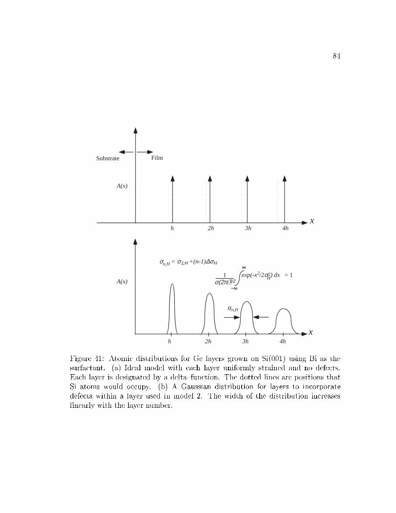
84
h 2h 3h 4hx
FilmSubstrate
A(x)
exp(-x2/2σ2) dx = 1
-σ(2π)1/2
σn,H
h 2h 3h 4h
σn,H = σ1,Η +(n-1)∆σΗ
x
A(x)1 H
Figure 41: Atomic distributions for Ge layers grown on Si(001) using Bi as thesurfactant. (a) Ideal model with each layer uniformly strained and no defects.Each layer is designated by a delta{function. The dotted lines are positions thatSi atoms would occupy. (b) A Gaussian distribution for layers to incorporatedefects within a layer used in model 2. The width of the distribution increaseslinearly with the layer number.

85
0.8
0.6
0.4
0.2
0.0
Cohe
rent
Fra
ctio
n
1086420
Coverage(ML)
F004
F022
fit F004
fit F022
Figure 42: Fits to data (dots) for F004 and F022 using non{uniform static Debye{Waller factor as in model 2.

86
The Ge atoms can have slight deviations from their expected positions. If
we assume that these deviations have a Gaussian distribution about the expected
lattice positions then PH will not change but FH will be lowered. These defects
can be taken into account by the static Debye{Waller factor DsH .
The origin of the defects is quite possibly from the local relaxation of Ge lattice
that is tetragonally distorted. These defects increase in magnitude as more layers
of Ge are grown. The width �n;H thus increases as the number of Ge layers increase.
The anisotropy along the [004] and [022] directions for �n;H can be understood from
the constraints due to the Si lattice. The [004] direction is normal to the growth
plane while [022] is o�{normal and therefore has an in{plane component. In{plane
the Ge atoms are constrained by the underlying Si lattice which is presumably
defect free. The Ge atoms are �xed to the Si lattice positions in{plane and therefore
strained because of the lattice mismatch. In{plane the Ge atoms are less likely
to deviate from their positions as that would require modifying the underlying
Si lattice. Along the [004] direction there is no stress and so the Ge atoms take
positions di�erent from the Si lattice. The Ge atoms take positions that would
minimize the total strain energy. Variations in Ge atomic positions along the [004]
direction do not signi�cantly a�ect the in{plane lattice structure. Therefore the
Ge atoms are more likely to deviate along the [004] direction. We interpret the
lower width for �n;022 from its in{plane component. Assuming an ellipsoid one can
calculate the in{plane widths �n;k using the values of �n;004 and �n;022 from model
2 as
1
�2n;k=
2
�2n;022� 1
�2n;004: (35)
Since in model 1 individual layers are not considered it may be more applicable

87
for lower (< 3 ML) Ge coverages. At higher Ge coverages the topmost Ge layers
are likely to be more defective than the Ge layers close to the Si substrate and
therefore model 2 may be more applicable.
6.3.3 E�ect of surfactant
Ge layers grown on a Si(001) surface without surfactants has been extensively
studied. It has been now accepted that Ge grows up to 3ML pseudomorphically
and thereafter relaxes by island formation. To date there is no reported XSW
study of Ge �lms grown beyond 1 ML without surfactants. We attempted to do
a similar study on samples grown without Bi as a surfactant for comparison. As
far as ex situ measurements are concerned there is a problem. To protect the Ge
in open air a Si cap layer has to be grown on top of it. But due to the lower
surface energy of Ge than that of Si, Ge segregates into Si to the surface. A direct
comparison is therefore not available. The Ge segregation can be inhibited in the
absence of any surfactant by growing the samples at room temperature or below.
But low temperature growth has shown to result in many defects and generally
poor crystallinity. This problem can be solved by performing the measurements in
UHV where there is no need for a protective cap layer. We have recently acquired
such a capability and therefore it is a topic of future experiments.
We looked at one sample that had 1ML of Ge, buried under a Si cap, grown
without Bi but otherwise under identical growth conditions. The XSW measure-
ments for 1ML Ge without Bi and 1.6 ML Ge with Bi are shown in �gure 43. Even
though the Ge coverage in the SME grown sample is higher , we measured higher
coherent fraction and coherent position than for the non{SME grown sample. This
clearly shows that Bi prevented segregation of Ge in Si cap as also con�rmed by

88
3.0
2.5
2.0
1.5
1.0
0.5
0.0
Normalized Flourescence Yield
3020100-10(θ−θB) µrad
4
3
2
1
0
Ref
lect
ivity
1.6 ML with Bifc = 0.822 ± 0.01
pc = 1.063 ± 0.003
1.1 ML no Bifc = 0.639 ± 0.01
pc = 1.026 ± 0.003
Si(004), Ge KαEγ = 12.5 keV
Figure 43: Angular dependence of (004) XSW data (markers) and best �t (solidlines) for Ge K� uorescence yield and re ectivity for 1.6 ML Ge with Bi and 1.1ML without Bi on Si(001).

89
our in situ LEED and AES observations (see chapter 4). The lower coherent frac-
tion and coherent position for non{SME growth is consistent with Ge segregation
in Si.
6.3.4 XSW (008) Measurement
XSW measurements can be used to calculate the root mean square thermal vibra-
tional amplitudes of adsorbate atoms [71]. Two XSW measurements are necessary
to calculate the vibrational amplitude along a particular H direction. Therefore
the combination of a (004) and a (008) measurement on the same sample can be
used to calculate the vibrational amplitude along the [001] direction. Lyman et
al [72] have used (008) and (004) re ections to calculate the RMS vibrational am-
plitude of adsorbates. Ideally the coverage of the adsorbate should be less than 1
ML so that there is only one unique position i.e. a004 = 1. Although we did not
have such a sample we did (008) measurement for the 1.7 ML Ge sample as it had
the highest coherent fraction. (The 1 ML Ge sample grown without Bi was not
suitable because a signi�cant amount of Ge had segregated into the Si cap layer.)
The root mean square vibrational amplitude can be written as
hu2001i = �d20046�2
ln
�F008
F004
cos(�p004)
cos(n�p004)
�(36)
where n = 1:7 is the number of layers. Figure 44 shows the XSW measurements
for the (004) and (008) re ections at E = 11:2 keV. Note that P008 = 2P004 since
d004 = 2d008. Using our XSW measured values of F008 = 0:36 and F004 = 0:81
we calculate from equation 36 a room temperature RMS vibrational amplitude ofphu2001i = 0:15 � 0:01 �A. This value is higher than the bulk thermal vibrational
amplitude for bulk Ge� 0:068 �A calculated using Debye temperature of 360 K [73].

90
Without changing the temperature, one cannot separate the thermal vibrational
amplitude and static width �H . Therefore our above measurement ofphu2001i also
has a contribution from the static DW e�ect. The di�erence between our measured
value ofphu2001i = 0:15 �A and the bulk vibrational amplitude is 0.08 �A. This can
be considered as the value for �004 for 1.7 ML Ge coverage.
The (008) rocking{curve width is much narrower than the (004) and therefore
very sensitive to angular drift. To avoid the sample drift problem we scanned
the piezo driven rotary stage motor of the �rst Si(008) channel cut of the post
monochromator. The rotation of second Si(008) channel cut which was locked by
electronic feedback to the �rst one then followed automatically. This constitutes
an energy scan with a very narrow range 0.07 eV that is much smaller than the
energy bandpass 2.95 eV from the high{heat load Si(111) monochromator.
6.4 XSW Results of Si Cap
At a growth temperature above 350ÆC the Si cap layer above the Ge should be
epitaxial and have the same lattice constant as the Si substrate if the Ge layer
is pseudomorphically strained. The Si cap lattice will be shifted with respect to
the Si substrate lattice by h+ h0 where h is the position of the top most Ge layer
and h0 is the additional height due to the di�erence between Si{Si and Si{Ge bond
lengths. The XSW determination of the displacement of the Si cap with respect
to the Si substrate is another way to study the strain in the buried Ge �lm.
6.4.1 X-ray evanescent wave e�ect
To measure the cap displacement by the XSW technique the Si K� signal from the
cap should be e�ectively isolated from the strong Si K� signal from the bulk. This

91
2.0
1.5
1.0
0.5
0.0
Normalized Yield
20151050 (θ−θB) µrad
4
3
2
1
0
Reflectivity
fc = 0.40 ± 0.02
pc = 0.137 ± 0.01
Si(004), Ge Kα Eγ = 11.2 keV
2.5
2.0
1.5
1.0
0.5
0.0
Normalized Yield
3020100-10
4
3
2
1
0
Reflectivity
fc = 0.80 ± 0.02pc = 0.064 ± 0.01
Si(004), Ge Kα Eγ = 11.2 keV
Figure 44: Angular dependence of (004) (top) and (008) (bottom) XSW data andbest �t (solid lines) for normalized Ge K� and uorescence yield and re ectivityfor 1.7 ML Ge grown with Bi on Si(001).

92
αα’
z
n = 1
n = 1- δ - iβ
Figure 45: X{ray evanescent wave emission e�ect to probe surface layers.
could be accomplished by using the surface sensitivity of photoelectron emission.
With the usual XSW technique based on uorescence measurements the surface
sensitivity required can be achieved by using the evanescent wave{emission (EW)
e�ect. This EW e�ect was �rst demonstrated by Becker et al [56] and later com-
bined with the XSW method and used to measure buried layers by Lee et al [74].
The emitted uorescent x{rays are refracted at the surface as show in �gure 45.
X{rays undergo total external re ection when � = �c, �0 = 0, where �c is the
critical angle. For � � �c the emission is explained by an exponentially damped
evanescent wave. Using the optical reciprocal principle the intensity Iout of the
uorescence x{ray emitted from depth z below the surface as a function of angle
is given by
Iout(�; z) / Is(�)e��z(�)z (37)
where Is is the intensity of the uorescence x{ray emitted from the surface. The
\e�ective" linear absorption coeÆcient �z is related to the index of refraction
n = 1� Æ � i� as [74]

93
10
100
1000
2.52.01.51.00.50.0 α
αc
EscapeDepthZ(� A)
= 0:9Æ
(Æ)
Figure 46: Escape depth of Si K� uorescence in Si as function of take{o� angle.
�z =4�p2�2
f[(2��2)2+4�2]1=2+2��2g1=2 for�� �c �z = �0z= sin�: (38)
The Si K� energy is 1:74 keV and the critical angle for this wave in Si is �c =p2Æ = 0:9Æ. Figure 46 shows the calculated escape depth Z = ��1z as a function of
take{o� angle �. Z has a minimum value of 36 �A at � = 0 and then dramatically
increases at � = �c This abrupt reduction in the escape depth below the critical
angle makes this technique surface sensitive. All our samples had approximately
a 100 �A thick Si cap layer on top of the Ge layer. Below the critical angle at
about 0:9Æ the uorescence x-rays emitted from the Si substrate will not reach the
detector.
The XSW measurements of the Si cap were done using a slit in front of the
solid state uorescence detector. The slit was scanned vertically and the Si K�
uorescence was monitored. The slit was then positioned so that the take{o� angle
was just below the critical angle. XSW measurements for the (004) re ection were

94
then carried out as usual. To verify that the contribution to the Si uorescence
signal from the substrate was negligible the slit was lowered further by approx-
imately 0:1Æ and the measurements were repeated. The absence of any change
in the measured Si coherent position indicated that the Si uorescence from the
substrate was negligible. Measurements were done on samples with 1.1 ML, 1.6
ML, 3.0 ML, and 3.4 ML of Ge coverage. The XSW measurements are shown in
�gure 47 and �gure 48. Table 3 shows the measured values of FC and PC for the
various samples.
If the Ge �lm is completely strained and pseudomorphic and the Si cap is
unstrained and epitaxial then the (004) planes of the Si cap will be shifted with
respect to the Si substrate (004) planes, exactly by the sum of coherent positions
for the topmost and the �rst Ge layers. This is assuming that there are an inte-
ger number of Ge layers. The coherent positions of the cap layers based on our
measured Ge coverage and our measured Ge coherent positions are also shown for
comparison in table 3.
Unlike the earlier reported case of 1 ML In buried in GaAs(001) [74], these
XSW cap displacement measurements for buried Ge in Si(001) are smaller than
expected. Interestingly, for the samples grown with Bi as the surfactant (see
table 3), P cC � P a
C = 0:06 � 0:01 �A. This is equal to the coherent position for
the �rst Ge atomic layer. With our limited number of measurements we cannot
explain this e�ect. Future experiments for higher Ge coverages are required to
verify its validity and to explain it.

95
2.5
2.0
1.5
1.0
0.5
0.0
Normalized Yield
40200-20(θ−θB)µrad
4
3
2
1
0
Ref
lect
ivity
fc = 0.815 ± 0.02
pc = 0.043 ± 0.01
Si(004), Si Kα Eγ = 8.0 keV
2.5
2.0
1.5
1.0
0.5
0.0
Normalized Yield
40200-20
4
3
2
1
0
Ref
lect
ivity
fc = 0.848 ± 0.02
pc = 0.073 ± 0.01
Si(004), Si Kα Eγ = 8.0 keV
Figure 47: XSW cap measurements for 1.6 ML Ge coverage (top) and 1.1 ML Gecoverage (bottom) performed at 8.0 keV.

96
2.5
2.0
1.5
1.0
0.5
0.0
Normalized Yield
40200-20(θ−θB)µrad
3.5
3.0
2.5
2.0
1.5
1.0
0.5
0.0
Ref
lect
ivity
fc = 0.440 ± 0.02
pc = 0.177 ± 0.01
Si(004), Si Kα Eγ = 8.0 keV
2.5
2.0
1.5
1.0
0.5
0.0
Normalized Yield
40200-20
2.5
2.0
1.5
1.0
0.5
0.0
Ref
lect
ivity
fc = 0.426 ± 0.02
pc = 0.215 ± 0.01
Si(004), Si Kα Eγ = 8.0 keV
Figure 48: XSW cap measurements for 3.4 ML Ge coverage (top) and 3.0 ML Gecoverage (bottom) performed at 8.0 keV.

97
Coverage Bi F aC P a
C P bC P c
C
(ML) Surfactant? �0:02 �0:01 { �0:021.1 No 0.815 0.043 0.126 0.052
1.6 Yes 0.848 0.073 0.129 0.126
3.0 Yes 0.440 0.177 0.266 0.244
3.4 Yes 0.426 0.215 0.308 0.270
Table 3: Results of (004) XSW measurements for the Si cap.a Measured values, b
from continuum elasticity theory and c based on measured Ge P004 values.

Chapter 7
Ge Growth on Patterned Si(001)
7.1 Introduction
Recently there has been much interest in the study of self assembled semiconduc-
tor nano{dots also know as quantum dots. Although the important properties of
nano{dots and their technological potential were understood for some time, the
fabrication of nano{dots has been turned out to be diÆcult until recently. In the
past lithographic techniques were employed to fabricate quantum dots. Although
there have been vast improvements in fabricating nanometer{scale structures, fab-
rication of device-quality nanostructures is still a challenge. Growth of quantum
dots by self assembly is very attractive both scienti�cally and technologically. The
Stranski{Krastanov growth mode [6] can be used to grow nano{dots that are self{
organizing and self{limiting in size [67].
98

99
7.2 Electronic properties
When the size of a solid becomes comparable to the de Broglie wavelength of
charge carriers (electrons and holes), they see a con�nement potential which dras-
tically alters the electronic and optical properties of the system. The continuous
spectrum of electronic density of states becomes discrete. The discrete energy lev-
els are like from atoms and sometimes quantum dots are referred to as \arti�cial
atoms" [75]. In solids the quantum con�nement e�ect is observed for size in the
range of 1{100 nm. Electron transition between the discrete levels produces sharp
photoluminescence lines. These discrete energy levels for example can be the basis
of a semiconductor laser that can achieve the luminosity and coherence of a gas va-
por laser. Variations in the size and shape of the nano{dots will smear the discrete
edges degrading their optical and electronic properties. Therefore a high degree of
homogeneity in size, shape and strain at macroscopic length scales is essential to
achieve usable performance from quantum dot devices.
7.3 Self assembled Ge island growth on Si(001)
The 4:2% lattice mismatch between Ge and Si results into Ge quickly forming
3{D islands for coverages higher than 3{4 ML. After the �rst reports of coherent
growth of Ge islands on Si [2], this system has been extensively studied. The
strain relaxation in these coherent islands is achieved by elastic deformation of the
substrate. In chapter 1 we looked at the growth of Ge islands on Si(001). We will
look at some of the studies done on this system [18, 83, 84].

100
7.3.1 Island distribution
After the early reports of Ge island formation on Si(001) [2] the evolution and
distribution of size and shape of the islands recently has been extensively studied
by R. S. Williams and co{workers at HP Laboratories. In their studies they report
three kinds of 3D islands [83, 84]. For growth temperatures between 550 to 650ÆC,
the 3D islands initially have f105g facets and rectangular base, with their edges
along the h100i directions [18]. As the islands grow they become dome shaped with
more facets, f113g, f102g and f518g along with f105g and f001g facets appear andthe base becomes polygonal [76]. Further growth results into larger shaped domes
called superdomes with presumably f111g or similar facets. Figure 49 shows the
AFM image and distribution of di�erent shapes of islands observed by Williams et
al after depositing 13 ML of Ge onto Si(001) and annealing for 30 min at 550ÆC.
They have reported transitions between the di�erent island shapes as a function
of substrate temperature and Ge coverage. They experimentally determined the
shape diagram as shown in �gure 49 as a function of Ge coverage and temperature.
K�astner et al found that at lower temperature (300ÆC) and coverages only 1-2
ML beyond the wetting layer kinematic limitations prevent formation of larger
islands and smaller islands with only f105g facets are formed [79]. Although they
pointed out that such a kinetic limitation should favor a narrow island distribution
they observed continuous nucleation of new islands [79]. The island distribution
also depends on annealing times. At lower temperatures and longer annealing
times, the islands evolve to a relatively stable, steady-state distribution while at
higher temperatures alloying of Ge and Si determines the island shape [77]. Alloy-
ing decreases the mis�t between the islands and the substrate and larger islands
appear. It also delays the onset of dislocations in the islands [78].

101
The size distribution of the islands is still not very well understood and cur-
rently two di�erent views exist. One model views the island size and distribution
is based on kinetic process of Oswald ripening [80, 81, 82]. Real time TEM by
Ross et al during Ge growth on Si(001) by chemical vapor deposition at 650ÆC
shows that island size changes continuously over time [81]. Another model con-
siders the islands to be in thermodynamic equilibrium with each other [83]. Thus
according to the second model pyramids and domes correspond to two energetically
stable island con�gurations of strained coherent islands. The observations of Ross
et al are not consistent with the second model. The inconsistency could be due
to Ge islands being metastable with respect to alloying with the substrate [76].
Alloying decreases the mis�t and increases the critical island size. In addition
even at constant temperature alloying may vary with deposition time. Apart from
growth temperature and time alloying seems to depend on the strain energy [78].
Domes have higher strain energy densities and alloy at lower temperatures than
pyramids [78]. On annealing at 650ÆC domes have been observed to transform
reversibly into pyramids of larger size due to alloying [84].
The composition and thickness of the Ge wetting layer is also not well un-
derstood at higher temperatures. If the wetting layer is metastable then during
annealing the islands can grow from migration of Ge atoms from the wetting layer
into the islands [77]. As with pyramids and domes the wetting layer is also ex-
pected to undergo alloying and its critical thickness should presumably increase as
well. If this is correct then the alloying of the Ge wetting layer should occur �rst
as it has the largest strain energy density.

102
Figure 49: After Williams et al [76] (a) Atomic force microscope topograph of a 13eq-ML �lm of Ge deposited onto Si(001) and annealed for 30 min at 550ÆC. Thegray scale is keyed to the local facet angle with respect to the substrate plane, withdarker shades corresponding to steeper angles. Pyramids, domes and superdomesare readily recognized by both their size and shading. (b) scatter plot showing theexposed surface area of the islands versus their volumes on a 1�m2 area for thesame sample as in part a. Each island shape forms a family of points on the graph,allowing the members of each family to be identi�ed for statistical analysis.

103
7.3.2 Lateral ordering
The islands interact with each other through the substrate [85]. TEM studies have
shown that the islands generate signi�cant strain �elds around them in the sub-
strate [2, 86]. These strain �elds cause the islands to repel each other [87]. LeGoues
et al have reported real time observation of small islands repelled by larger islands
as the boundaries of their base approach each other [88]. Elastic interaction be-
tween the islands can make them stable against transformation to larger islands or
domes [89]. Thus strain due to lattice mismatch can lead to narrower distribution
of islands with uniform island{island spacing. This strain �eld interaction can also
lead to short{range ordering of the islands on the substrate [90]. Such lateral or-
dering is observed for Si1�xGex/Si(001) at low values of x (x = 5�15%) by Dorsch
et al [91]. Due to the low mis�t they observed ripples which self{organize along the
(100) directions. On further growth they saw the ripples transform into coherent
islands. The base of the islands was determined by the initial ripple pattern. They
measured the wavelength of the periodic separation of islands to be 6:5�m at 5%
Ge content to 1:1�m at 15% Ge content.
Schmidbauer et al [90] have investigated the ordering of self{assembled Si1�xGex
islands by grazing incidence small{angle x{ray scattering and AFM. They saw
superstructure satellite peaks along the (100) directions in the power spectrum of
AFM images indicative of lateral ordering of islands (see �gure 50 a). They also
observed satellite peaks along the h100i and h110i directions in their GISAXS scans(see �gure 50 b). They found increase in ordering as the island density increased.
Due to larger mis�t for pure Ge the lateral ordering is short range.

104
Figure 50: Schmidbauer et al [90], (a) Power spectrum of AFM micrograph and(b) GISAXS intensity pro�le along h100i and h110i for Si1�xGex (x = 0:25) islandson Si(001).

105
7.3.3 Vertical ordering
In heteroepitaxial systems with larger mis�ts island formation on the surface is
favored where the the strain at the surface reduces the mismatch between the island
and the surface [64]. Alternating growth of islands and substrate material, the
islands in successive layers become spatially correlated [92]. Terso� et al [64], gave
a generic model based on continuum elasticity theory to explain the correlation
between islands in successive layers. They modeled the surface strain � at lateral
position x from an island buried at a depth L and x = 0 to be
�(x) = C(x2 + L2)�3=2[1� 3L2=(x2 + L2)] (39)
Where C takes into consideration the volume of the island, the mis�t and the elastic
constants. Their model correctly explained the increase in uniformity of the island
size and spacing for successive layers. They grew Si0:25Ge0:75/Si superlattices and
found that the islands became more regular and uniformly spaced after 20 layers
compared to �rst layer (see �gure 51). Some variation in size and shape and spacing
is still evident in their AFM images. It is not clear if the model is valid for large
number of layers as it assumes the surface to be isotropic (only x as independent
variable).
7.4 Growth of Ge on patterned Si(001)
Randomly distributed islands of uniform size and shape may be adequate for op-
tical applications of quantum dots, but for electronic applications precise control
over positioning of these islands is required. Although as discussed in section 7.3.3
superlattice structures of islands can be used to position islands on the surface,

106
Figure 51: Terso� et al [64], AFM images of Si0:25Ge0:75/Si superlattices. Scanningdirection is [110]. (a) 0:8�m �0:8�m image after deposition of the �rst alloylayer;(b) 1:25�m �1:25�m image after deposition of the 20th alloy layer.

107
there is still no control over the period and many layers are required to get islands
with good uniformity. Such a process is not economical and poses innumerable
problems for integrating devices.
A combination of lithography and SK growth mode has been shown to achieve
improved control in positioning the islands and making them more uniform [93, 94,
95, 96]. The key idea in the work by Kamins et al and later by Jin et al is to control
coarse positioning of islands by conventional lithography and then use mis�t strain
to �ne tune the position, size and shape of the islands. On an in�nite surface the
Ge islands are coupled to each other through their di�usion on the surface [97]
and the strain �elds they generate in the substrate. The di�usion lengths for Ge
on Si(001) are quite large at higher temperatures. Strain �elds on the other hand
are localized near the islands. Therefore di�usion coupling between islands tend to
be long range compared to strain coupling. Isolating the island nucleation site by
putting barriers to di�usion or modifying it to some degree can lead to dramatic
change in the way the islands grow. One such barrier to di�usion is to make the
surface dimensions comparable to the di�usion lengths. Patterned surfaces either
by selective area growth or etching can isolate nucleation of islands from each
other.
Patterning of substrates has been shown to e�ect the growth of Ge on Si(001).
At higher growth temperatures (> 600ÆC) Ge di�uses readily on Ge surface and
presumably nucleates along the edges. This nucleation takes place due to the
di�usion barrier presented by the edge and is a�ected by the vicinal surface. Any
defects such as dislocations at the edges also results in nucleation. The edge thus
o�ers a site for formation of Ge islands on Si. Along the edge the Ge dots can
arrange themselves in a periodic manner due to island{island interaction through
strain �elds produced by the islands in the substrate. There exist as a function of

108
growth conditions a distribution of the size of the islands and the island to island
separation.
7.4.1 Growth on stripe{mesas
Kamins et al [93, 94] investigated the growth of Ge islands on Si stripe{mesas. The
Si stripe mesas were formed by selective area growth by chemical vapor deposition.
Ge islands were then deposited also by CVD at 600ÆC. The Si lines on their samples
were oriented along the h100i and h110i directions and had widths ranging from
450 nm to 10�m. They observed ordering of Ge islands near the edges of the
Si(001) stripe{mesas (see �gure 52). For higher coverages the additional rows of
Ge islands appeared away from the edges but with decreasing order. The islands
were about 75 nm in size. When the Si surface was a narrow ridge they observed
only one row of Ge islands. They saw better ordering on h100i{directed lines
than on h100i lines. It is not clear what was the shape of the islands as they did
not show any high resolution images of individual islands. From their images the
islands looked dome shaped rather than pyramidal. Jin et al [96] observed similar
ordering of Ge islands.
The ordering of Ge islands on patterned surfaces could be because of several
factors. Kamins et al suggested easy nucleation of Ge atoms at atomic steps on the
shallow facets of Si stripe{mesas close to the edges. Re ection of Ge atoms from
the edges perhaps increases the concentration of Ge adatoms near the edges with
the consequent higher probability of nucleation [93]. It is also possible that close
to the edges the defect density is higher which in turn leads to greater nucleation
of Ge islands. The easier deformation of the Si lattice near the edges also can
explain favorable Ge nucleation. No Ge islands were observed in the center of the
islands mainly due to strong Ge di�usion. The island spacing along the edges is

109
Figure 52: Kamins et al [93], AFM images of Ge islands grown on Si stripe{mesasshowing ordering of several rows of Ge islands near the edges of the at Si(001)surface. Widths of Si(001) surface: (a) 670 nm, (b) 1.0�m, (c) 1.7�m .

110
very uniform for the �rst row mainly due to strain driven self{assembly.
7.4.2 Growth on square{mesas
Growth of Ge islands on square{mesas in principle is similar to that on Si stripe{
mesas except now the di�usion of Ge atoms is limited in both x and y directions.
Jin et al [96] have studied the growth of Ge islands on Si square{mesas. At lower
coverage they found four islands formed at the corners of the square{mesa (see
�gure 53). At suÆcient coverage an additional �fth island was formed in the
central region. They report the central island to be pyramidal as opposed to dome
shaped outer islands.
7.5 In situ LEED Studies
We performed in situ low energy electron di�raction studies of Ge island growth
by MBE on planar Si(001) surface. The samples were prepared in our UHV{MBE
chamber. The preparation of growth surface and the MBE growth is explained in
chapter 4. Two di�erent studies were performed: one as function of Ge coverage
at �xed growth temperature of 650ÆC and other at �xed Ge coverage of 10 ML. In
each case the LEED was performed at room temperature.
7.5.1 Coverage dependence
The coherent Ge islands have faceted surfaces. The islands are believed to be on
top of a Ge wetting layer 3{4 ML thick. The transition from 2D to 3D growth as
the Ge coverage is increased will change the surface reconstruction. During the
2D growth the normal 2{domain 2� n reconstruction is expected [98]. When 3D
growth begins the tilted surfaces of the islands will produce additional patterns in

111
Figure 53: Jin et al [96], (a) A 3D AFM image with four Ge islands located at thecorners on square mesa with the base lines parallel to the h110i directions. TheGe thickness is 9 ML. (b) A 3D AFM image with �ve Ge islands with 10 ML Ge.The �fth pyramidal island is formed in the central region.

112
the LEED image. Figures 54 and 55 show the LEED images taken after di�erent
coverages of Ge deposited at 640ÆC.
After about 3 ML of Ge is deposited a 2 � n reconstruction was seen with
n � 7. At this coverage the Ge growth is still 2D but the usual 2�1 reconstruction
changes to 2�n to reduce the number of dangling bonds as originally proposed by
Pandey [99]. At 5 ML additional spots appear in the di�raction pattern. These
peaks have 4{fold symmetry and are collinear with the h11i directions which is
same as the h100i directions of the Si lattice. Additionally energy scans of the
LEED showed that these spots moved with respect to the 2 � 1 LEED pattern.
This indicated that the additional peaks were from the faceted surfaces intersecting
the (001) surface along the h100i directions. Our LEED observations and analysis
agree with the f105g faceting of Ge islands on Si(001) reported in literature. At
12 ML the Ge island density is higher and therefore the peaks from the faceted
surfaces become more intense.
7.5.2 Temperature dependence
The annealing studies were performed for 10 ML of Ge deposited at room tem-
perature. The sample temperature was then ramped at 1ÆC=s, held at a given
temperature for 10 min and then cooled down naturally to room temperature.
LEED was then performed. Figure 56 shows the LEED images taken after an-
nealing the sample at di�erent temperatures. In �gure 56a the LEED is that of
clean Si(001) reconstruction. At room temperature the Ge is mostly amorphous
and therefore no LEED pattern was observed. As the temperature was raised the
Ge started to become more crystalline and di�raction spots began to appear in the
LEED image. At about 525ÆC (�gure 56b) a faint 2 � 1 reconstruction appeared
probably from the wetting layer. The presence of high LEED background and no

113
Figure 54: LEED images after various coverages of Ge. (a) clean Si surface, 2{domain 2� 1 reconstruction, (b) after 3 ML of Ge 2� n reconstruction; cont'd. in�gure 55.

114
Figure 55: LEED images after various coverages of Ge, cont'd. from �gure 54 (c)after 5 ML of Ge additional spots with 4{fold symmetry due to the faceted surfaceson the islands appear, (d) after 12 ML of Ge the reconstruction is similar to (c)with higher intensity in the spots from faceted surfaces.

115
additional peaks other than the 2 � 1 pattern in �gure b indicates that on the
surface signi�cant amount of Ge remained amorphous and no islands were formed.
After annealing at 623ÆC islands were formed as as seen from the LEED pattern
in �gure 56c. This is in agreement with our observation in previous section.
The LEED pattern then remained stable up to around 775ÆC when the di�rac-
tion peaks from the islands began to disappear. At this temperature the di�usion
of Si from the substrate in the Ge is very high resulting in alloying. The thickness
of the wetting layer increases exponentially as the Si content in the SiGe alloy
increases. Therefore at higher temperatures the Ge islands are absorbed to form
a energetically more favorable thicker wetting layer. This can explain why the
di�raction spots from the islands disappeared in �gure 56c. At 852ÆC only the
wetting layer is present and the LEED pattern was 2 � n again consistent with
our observation for pure Ge wetting layer. After annealing at 900ÆC the LEED
pattern was pure 2� 1 as the Ge layer had completely and irreversibly absorbed
into the Si substrate (�gure 56f). Using the di�raction spots we calculated the
lattice constant of the alloy to be 3% larger than the Si lattice constant. Using
Vegards's law we estimated the alloy composition after annealing at 900ÆC to be
Si0:3Ge0:7.
7.6 Morphology Studies
We studied the morphology of Ge grown on Si (001) surface patterned into stripe{
mesas. The surface was patterned into stripe{mesas using e{beam lithography and
reactive{ion etching as explained in chapter 4. The stripe{mesas were 160�m long,
about 0:6�m wide and 0:2� 0:3�m tall. The separation between two neighboring
stripe{mesas was 1:0�m. Figure 57 shows the AFM image after RIE etching. The

116
Figure 56: (a) LEED image of clean Si(001) surface. (b){(f) LEED images afterannealing the the sample at temperatures indicated. The Ge coverage was �xedat 10 ML. All the LEED images were taken at RT.

117
Figure 57: AFM micrograph of Si surface patterned into a column of stripe{mesasby e-beam lithography and RIE.
total patterned surface was only 160� 160�m2. As seen the edges of the lines are
nor very sharp due to the limitations of the e{beam writer. The lines were pat-
terned along h100i and h110i directions. The Ge was grown in our MBE chamber
at 640Æ. The surface preparation and Ge growth is explained in chapter 4. Ap-
proximately 8{12 ML of Ge was deposited. Ge was also deposited on unpatterned
Si to compare the results. The coverage was estimated by timing the deposition.
All the samples were imaged by AFM ex situ at the Materials Research Center.
Figure 58 shows the AFM micrograph of the surface after depositing approx-
imately 15 ML of Ge. The scan area is 5 � 5�m2. A distribution of islands is
clearly visible. The largest islands are about 400 nm in size with square base with

118
Figure 58: AFM micrograph of Ge islands on unpatterned Si(001) surface. TheGe coverage is about 15 ML.
sides along the h100i directions. The smallest islands are about 100� 200 nm2.
The AFM micrograph of a patterned surface after depositing approximately 10
ML of Ge is show in �gure 59. Compared to �gure 57 the stripe{mesas have almost
disappeared. The surface has three distinct features: (a) pits (b) plateaus and (c)
islands. The pits are the regions from where Si was etched during RIE. The in
situ sample annealing at 900ÆC to prepare a clean surface prior to Ge deposition
modi�ed the patterned surface considerably. At 900ÆC the native oxide layer is
desorped. Depending on the oxide thickness which can be nonuniform because
of the lithography and etching the �nal clean surface will be di�erent from the
original surface. In addition at 900ÆC Si di�usion on the surface is also signi�cant.

119
Figure 59: AFM micrograph of Ge islands on patterned Si(001) surface. The islandrows are along h110i direction. The Ge coverage is about 10 ML.
Annealing at temperatures lower than 900ÆC did not completely remove carbon
and oxygen contamination from the surface necessary to grow Ge. The above two
factor we think were responsible for the attening of the surface.
Even after the surface is modi�ed the edges of the stripe{mesas were preserved
as evidenced from the aligning of the Ge islands. The islands clearly appear to have
grown along a line in one direction presumably the edge of the strip{mesas. The
separation between the lines of these islands is approximately same as the width
of the stripe{mesas. Compared to Ge grown on planar surface the Ge islands on
the patterned surface have a much narrower distribution in size and shape. Also
the island size is smaller and the shape of all islands is same.

120
Figure 60 shows a high resolution AFM micrograph of the islands. the island
rows are along h110i directions. The islands approximately have a square base andalso appear to be faceted. As marked in the �gure there are two rows of islands.
The �rst row on the left side has islands spaced uniformly along the edge and
they are all of the same size. The average spacing between the islands is about
100 nm and the size of the island is about 60 nm. A second row with relatively
bigger islands is also seen. The spacing between the islands in the second row
is not uniform. This is consistent with observations of Kamins et al [93]. The
uniform spacing between the islands in the �rst row is indicative of the fact that
along the edges the islands interact with each other presumably through strain
�elds generated in the substrates and self{assemble. The presence of an edge
increases the probability of nucleation [93] along it. After the �rst row is formed
the islands grow to there maximum size and second row begins to nucleate. The
second row is not as uniform because of the absence of any edge in the immediate
vicinity. The Ge atoms di�using from the center get scattered by the �rst row of Ge
islands. Unlike the straight edge scattering from islands is probably less ordered
consequently forming a less ordered second row of islands. Following the same
reasoning the relatively less uniform �rst row on the right hand side of the stripe{
mesa in �gure is due to an edge that is not straight. As the edge is not visible in
the AFM micrograph the above explanation cannot be veri�ed. Compared to the
�rst row the nucleation of islands in the second row is shifted. The islands in the
second row are formed next to the gaps between the islands in �rst row. No Ge
islands are formed in the center due to lower nucleation probability.
The region between the stripe{mesas is also island free. This is little bit surpris-
ing as that region is expected to have large nucleation sites due to etching. But
due to annealing at 900ÆC the defect density probably is reduced considerably.

121
Figure 60: High resolution AFM micrograph of Ge islands on patterned Si(001).The edges are along h110i direction. The Ge coverage is about 10 ML.

122
Also due to etching this region has large roughness � 10nm possibly retarding the
Ge surface di�usion [95]. The lack of suÆcient di�usion may have prevented Ge
island formation.

Chapter 8
Summary
8.1 Thesis Summary
In this thesis we studied the epitaxial growth of Si/Ge heterostructures on Si(001)
surface with Bi as a surfactant with x{ray standing wave technique, grazing inci-
dence x{ray di�raction and x{ray specular re ectivity using synchrotron radiation.
We also initiated a study to understand the growth mechanism of Ge nano{dot
structures on patterned Si(001) by MBE.
Traditionally XSW technique has been mainly used for studying surfaces. We
demonstrated how XSW technique can be used to do structural studies of �lms of
several atomic layers. We investigated the layer by layer growth of Ge on Si(001)
in the presence of Bi as a surfactant by performing Si(004) and Si(022) XSW
measurements. By comparing approximately 1 ML Ge growth with and without
Bi we showed that Bi prevents segregation of Ge in Si. Under the assumption of
layer by layer growth and continuum elasticity theory, our measured coverage for
Ge agreed with our measured coherent positions for (022) re ection up to 10 ML
of Ge coverage and for (004) re ection up to 7 ML of Ge coverage. The coherent
fractions were considerably lower than expected. We showed that the reduction in
123

124
coherent fraction can be explained by a static Debye{Waller factor. The simplest
interpretation of our XSW data is that each Ge atom is likely to have a static
displacement about its expected position. For this static displacement �eld we
assumed a Gaussian distribution centered about the expected Ge atomic position.
We further extended this model by a semi ad{hoc assumption that the static
deviation increases linearly with the Ge atomic layer distance from the Si substrate.
The partial physical basis for this assumption is that as the Ge layer distance
increases it becomes more and more relaxed. Using this model we explained the
reduction in coherent fraction. One important result is that the width of this
displacement distribution in the [022] direction is smaller than in the the [004]
direction. Our conclusion is that the Ge atoms are more deviated in the normal
direction to the surface than in the direction in the plane of the surface.
Using GIXD we found that with Bi as a surfactant the critical thickness for
pseudomorphic growth for Ge was increased to 7 ML. Even at 10 ML of Ge growth
no island formation was observed but the Ge layer was partially relaxed. In the
case when Bi was not used we clearly showed that the Ge was relaxed and a SiGe
alloy was formed due to the segregation of Ge into Si cap layer. Using x{ray
re ectivity we showed that the �lm roughness increases dramatically as the Ge
layer thickness increased from 7 ML to 10 ML. These measurements are consistent
with our XSW measurements.
We also studied the self assembly of Ge nano{dots on Si stripe{mesas by atomic
force microscopy. The goal here was to arrange the Ge nano{dots of identical size
and shape in a periodic array by combination of strain �eld interaction between
the islands and coarse{scale lithography. We showed that compared to growth
on planar surfaces the Ge dots are of approximately uniform shape and size and
aligned along the edges of the stripes.

125
8.2 Future Work
The XSW structural analysis I discussed is model dependent because of the limited
number of measurements I was able to perform. XSW is very unique because it does
not su�er from the well known phase problem. Temperature dependent and higher
order (e.g. similar to (008) we performed) XSW measurements can be performed
to get more accurate and direct picture of Ge/Si(001) and other similar systems.
Due to the Ge segregation in the Si cap I was not able to do a similar study for
the Ge grown without surfactant. Also depth dependent XSW measurements can
be performed by monitoring the photoelectron yield. All these experiments would
require a UHV environment which we now have available at the 5ID{C undulator
beamline of the APS. These experiments can be performed for other surfactants
like Te and Sb as well.
The growth of nano{dots is very interesting and very little is known about their
growth on patterned surfaces. Surfactants like Sn under certain conditions promote
island growth and therefore may also be used to grow such structures. To this date
there is no such study reported. All of my AFM studies were performed ex situ
and therefore surfaces of the nano{dots could not be studied at atomic resolution.
Currently we are in the process of combining our UHV{MBE system with a UHV{
STM/AFM system. In situ STM/AFM studies should give more clearer and deeper
picture of the growth of such nano{dots. With future improvements in x{ray
micro{focusing and micro{di�raction techniques it would be possible to study the
strain in individual nano{dots [100]. These studies can be extended to magnetic
nano{dots as well. The current availability of high brilliance synchrotron sources
for x{ray and even more intense fourth generation source that are proposed now
would make the study of magnetic nano{dots by x{rays possible.

References
[1] M. Copel, M. C. Reuter, E. Kaxiras, and R. M. Tromp, Phys. Rev. Lett., 63,632 (1989).
[2] D. J. Eaglesham and M. Cerullo Phys. Rev. Lett., 64, 1943 (1990).
[3] E. Bauer, Z. Kristallogr. 110, 372 (1958).
[4] F. C. Frank and J. H. van der Merwe, Proc. Roy. Soc. London A 198, 205(1949).
[5] M. Volmer and A. Weber, Z. Phys. Chem. 119, 277 (1926).
[6] I. N. Stranski and Von L. Krastanow, Akad. Wiss. Wien. 146, 797 (1938).
[7] E. Bauer and J. H. van der Merwe, Phys. Rev. B 33, 3657 (1986).
[8] E. Tourine and K. H. Ploog, Thin Solid Films, 42, 43 (1993).
[9] T. Narusawa and W. M. Gibson, Phys. Rev. Lett. 47, 1459 (1981).
[10] M. Asai, H. Ueba, and C. Tatsuyama, J. Appl. Phys. 58, 2577 (1985)
[11] P. C. Kelires and J. Terso�, Phys. Rev. Lett. 63, 1164 (1989).
[12] J. W. Matthews J. Vac. Sci. Technol. 12, 126 (1975).
[13] J. Terso�, Phys. Rev. B 43, 9377 (1991).
[14] L. N. Aleksandrov, R. N. Lovyagin, O. P. Pchelyakov, and S. I. Stenin, J.Cryst. Growth 24/25, 298 (1974).
[15] H. {J. Gossman, L. C. Feldman, and W. M. Gibson, Surf. Sci. 155, 413 (1985).
126

127
[16] K. Miki, K. Sakamoto, and T. Sakamoto, in Chemistry and Defects in Semi-
conductor Heterostructures edited by M. Kawabe, e. R. Weber, and R. S.Williams, MRS Proc. Symp. D (1989).
[17] A. A. Williams, J. M.C. Thornton, J. E. Macdonald, R. G. van Silfhout, J. F.van der Veen, M. S. Finney, A. D. Johnson, and C. Norris Phys. Rev. B, 43,5001 (1991).
[18] Y. -W. Mo, D. E. Savage, B. S. Swartzentruber, and M. G. Lagally Phys. Rev.Lett., 65, 1020 (1990).
[19] A. J. Steinfort, P. M. L. O. Scholte, A. Ettema, M. Nielsen, E. Landemark, D.-M. Smigies, R. Feidenhans'l, G. Falkenberg, L. Seehofer, and R. L. JohnsonPhys. Rev. Lett., 77, 2009 (1996).
[20] G. Medeiros{Ribeiro, T. I. Kamins, D. A. A. Ohlberg, and R. S. Williams,Phys. Rev. B, 58, 3533 (1998).
[21] K . Sakamoto, T. Sakamoto, S. Nagao, G. Hashiguchi, K. Kuniyoshi, and Y.Bando, Jpn. J. Appl. Phys. 26, 666 (1987).
[22] P. M. J. Mar�ee, K. Nakagawa, F. M. Mulders, and J. F. van der Veen, Surf.Sci. 191, 305 (1987).
[23] S. S. Iyer, J. C. Tsang, M. W. Copel, P. R. Pukite, and R. M. Tromp, Appl.Phys. Lett. 54, 219 (1989).
[24] E. Kasper and H. Jorke, in Chemistry and Physiscs of Solid Surfaces, editedby R. Vanselow and R. F. Howe (Springer Verlag, Berlin, 1988), p. 557.
[25] J. C. Bean, L. C. Feldman, A. T. Fiory, S. Nakahara and I. K. Robinson, J.Vac. Sci. Technol. A 2, 436 (1984).
[26] P. R. Berger, K. Chang, P. K. Bhattacharya, J. Singh and K. K. Bajaj, Appl.Phys. Lett. 53, 684 (1988).
[27] H. J. Osten, J. Klatt, G. Lippert, B. Dietrich, and E. Bugiel, Phys. Rev. Lett.69, 450 (1992).
[28] D. J. Eaglesham, F. C. Unterwald, and D. C. Jacobson, Phys Rev. Lett. 70,966 (1993).

128
[29] H. J. Osten, J. Klatt, G. Lippert, E. Bugiel, and S. Hinrich, Appl. Phys. Lett.60, 2522 (1992).
[30] M. Horn{von Hoegen, B. H. M�uller, A. Al{Falou, and M. Henzler, Phys. Rev.Lett. 71, 3170 (1993).
[31] M. Copel, M. C. Reuter, M. Horn{von Hoegen, and R. M. Tromp, Phys. Rev.B, 42, 11682 91990).
[32] B. Voigtl�ander, A. Zinner, T. Weber, and H. P. Bonzel, Phys. Rev. B 51, 7583(1995).
[33] R. I. G. Uhrberg, R. D. Bringans, R. Z. Bachrach, and J. E. Northrup, Phys.Rev. Lett. 56, 520 (1986).
[34] D. H. Rich, T. Miller, G. E. Franklin, T.{C. Chiang, Phy. Rev. B 39, 1438(1989).
[35] R. M. Tromp, and M. C. Reuter, Phys. Rev. Lett. 68, 954 (1992).
[36] D. Yu and A. Oshiyama, Phys. Rev. Lett. 72, 3190 (1994).
[37] F. K. LeGoues, M. Copel, and R. Tromp, Phys. Rev. B, 42, 11690 (1990).
[38] J. M. C. Thornton, A. A. Williams, J. E. Macdonald, R. G. van Silfhout, M.S. Finney, and C. Norris, Surf. Sci. 273, 1 (1992).
[39] P. C. Zalm, G. F. A. van de Walle, D. J. Gravesteijn, and A. A. van Gorkun,Appl. Phys. Lett. 55, 2520 (1989).
[40] K. Sakamoto, K. Kyoya, K. Miki, H. Matsuhata, and T. Sakamoto, Jpn. J.Appl. Phys. 32, L204 (1993).
[41] W. Rodrigues, O. Sakata, T.{L. Lee, D. A. Walko, D. Marasco, M. J. Bedzyk,J. Appl. Phys., accepted for publication (2000).
[42] S. Higuchi and Y. Nakanishi, Surf. Sci. Lett. 254, L465 (1991).
[43] X. W. Lin, Z. Liliental-Weber, J. Washburn, and E. R. Weber, A. Sasaki, A.Wakahara, and T. Hasegawa J. Vac. Sci. Technol. B 13, 1805 (1995).
[44] I.{S. Hwang, T.{C. Chang, and T. T. Tsong, Phys. Rev. Lett. 80, 4229 (1998).
[45] S. Higuchi and Y. Nakanishi, J. Appl. Phys. 71, 4277 (1992).

129
[46] T. Schmidt, J. Falta, G. Materlik, J. Zeysing, G. Falkenberg, and R. L. John-son, Appl. Phys. Lett. 74, 1393 (1999).
[47] T. Hanada and M. Kawai, Surf. Sci. 242, 137 (1991).
[48] W. C. Fan, N. J. Wu, and A. Ignatiev, Phys. Rev. B 45, 14167 (1992).
[49] H. P. Noh, Ch. Park, D. Jeon, K. Cho, T. Hashizume, Y. Kuk, and T. Sakurai,J. Vac. Sci. Technol. B 12, 2097 (1994).
[50] Y. Qian, M. Bedzyk, P. F. Lyman, T. {L. Lee, S. Tang, and A. J. Freeman,Phys. Rev. B, 54, 4424 (1996).
[51] S. Tang, and A. J. Freeman, Phys. Rev. B, 50, 1701 (1994).
[52] B. W. Batterman, Phys. Rev. 133, A759 (1964).
[53] J. Zegenhagen, Surf. Sci. Rep. 18, 199 (1993).
[54] Y. Qian, Ph.D. Thesis, Northwestern University (1995).
[55] A. Krolzig, G. Materlik, M. Swars, and J. Zegenhagen, Nucl. Instr. and Meth.219, 430 (1984).
[56] R. S. Becker, J. A. Golovchenko, and J. R. Patel, Phys. Rev. Lett. 50, 153(1983).
[57] R. Feidenhans'l, Surf. Sci. Rep. 10, 105 (1989).
[58] H. Dosch, B. W. Batterman, and D. C. Wack, Phys. Rev. Lett. 56, 1144(1986).
[59] P. S. Pershan and J. Als{Nielsen, Phys. Rev. Lett. 52, 749 (1984).
[60] M. Born and E. Wolf, Principles of Optics (Pergamon Press, 1980).
[61] A. Ishizaka and Y. Shiraki, J. Electrochem. Soc. 133, 666 (1986).
[62] T. N. Rhodin and J. W. Gadzuk, The Nature of the Surface Chemical Bond,pp 113{273 (North{Holland, 1979).
[63] The LEED images are similar to that in �gure 55.
[64] J. Terso�, C. Teichert and M. G. Lagally Phys. Rev. Lett., 76, 1675 (1996).

130
[65] R. L. Headrick, J.-M Baribeau, D. J. Lockwood, and T. E. Jackman, M. J.Bedzyk, Appl. Phys. Lett. 62, 687 (1993).
[66] P. F. Lyman and M. J. Bedzyk, Appl. Phy. Lett., 69, 978 (1996).
[67] V. A. Shchukin, N. N. Ledentsov, P. S. Kop'ev, and D. Bimberg Phys. Rev.Lett., 75, 2968 (1995).
[68] M. Takahasi, S. Nakatani, T. Takahashi, X. Zhang, M. Ando, S. Fukatsu, andY. Shiraki, Jpn. J. Appl. Phys. 34, 2278 (1995).
[69] J. Falta, D. Bahr, G. Materlik, B. H. M�uller, and M. Horn{von Hoegen, Appl.Phys. Lett. 68, 1394 (1996).
[70] J. Hornstra and W. J. Bartels, J. Cryst. Growth 44, 513 (1978).
[71] M. J. Bedzyk, G. Materlik, Phys. Rev. B 31, 4110 (1985).
[72] P. F. Lyman, Y. Qian, T.-L. Lee, M. J. Bedzyk, Physica B 221, 426 1996.
[73] N. W. Ashcroft and N. D. Mermin, , Solid State Physics, pp. 461 (SaundersCollege, 1976).
[74] T.-L. Lee, Y. Qian, P. F. Lyman, J. C. Woicik, J. G. Pellegrino, and M. J.Bedzyk, Physica B 221, 437 (1996).
[75] X. Deng and M. Krishnamurthy, Phys. Rev. Lett. 81, 1473 (1998).
[76] R. S. Williams, G. M-. Ribeiro, T. I. Kamins, and D. A. A. Ohlberg, J. Phys.Chem. B, 102, 9605 (1998).
[77] T. I. Kamins, G. M-. Ribeiro, D. A. A. Ohlberg, and R. S. Williams, J. App.Phys., 85, 1159 (1999).
[78] S. A. Chaparro, J. Drucker, Y. Zhang, D. Chandrasekhar, M. R. McCartney,and D. J. Smith, 83, 1199 (1999)
[79] M. K�astner and B. Voigtl�ander, Phys. Rev. Lett., 82, 2745 (1999).
[80] J. Terso�, F. K. LeGoues, Phys. Rev. Lett., 72, 3570 (1994).
[81] F. M. Ross, J. Terso�, R. M. Tromp, Phys. Rev. Lett., 80, 984 (1998).
[82] M. Z-. Allmang, L. C. Feldman, M. H. Grabow, Surf. Sci. Rep., 16, 381 (1992)

131
[83] G. M-. Ribeiro, A. M. Bratovski, T. I. Kamins, D. A. A. Ohlberg, and R. S.Williams, Science, 279, 353 (1998).
[84] T. I. Kamins, G. M-. Ribeiro, D. A. A. Ohlberg, and R. S. Williams, Appl.Phys. A, 67, 727 (1998).
[85] V. A. Shchukin, N. N. Ledentsov, P. S. Kop'ev, and D. Bimberg, , 75, 2968(1995).
[86] O. V. Kolosov, M. R. Castell, C. D. Marsh, and G. A. D. Briggs, Phys. Rev.Lett., 81, 1046 (1998).
[87] H. T. Johnson and L. B. Freund, J. Appl. Phys., 81, 6081 (1997).
[88] F. K. LeGoues, M. C. Reuter, J. Terso�, M. Hammar, and R. M. Tromp,Phys. Rev. Lett., 73, 300 (1994).
[89] J. A. Floro, G. A. Lucadamo, E. Chason, L. B. Freund, M. Sinclair, R. D.Twesten, and R. Q. Hwang, Phys. Rev. Lett. 80, 4717 (1998).
[90] M. Schmidbauer, Th. Wiebach, H. Raidt, M. Hanke, and R. K�ohler, Phys.Rev. B 58, 10523 (1998).
[91] W. Dorsch, B. Steiner, M. Albrecht, H. P. Strunk, H. Wawra, G. Wagner, J.Cryst. Growth, 183, 305 (1998).
[92] Q. Xie, A. Madhukar, P. Chen, and N. P. Kobayashi, Phys. Rev. Lett. 75,2542 (1995).
[93] T. I. Kamins and R. S. Williams, Appl. Phys. Lett. 71, 1201 (1997).
[94] T. I. Kamins, R. S. Williams, and D. P. Basile, Nanotechnology 10, 117(1999).
[95] T. I. Kamins, D. A. A. Ohlberg, R. S. Williams, W. Zhang, and S. Y. Chou,Appl. Phys. Lett. 74, 1773 (1999).
[96] G. Jin, J. L. Liu, S. G. Thomas, Y. H. Luo, and K. L. Wang, Appl. Phys.Lett. 75, 2752 (1999).
[97] J. R. Heath, R. S. Williams, J. J. Shiang, S. J. Wind, J. Chu, C. D'Emic, W.Chen, C. L. Stanis, and J. J. Bucchignano, J. Phys. Chem. 100, 3144 (1996).

132
[98] U. K�ohler, O. Jusko, B. M�uller, M. Horn{von Hoegen, and M. Pook, Ultra-microscopy 42{44, 832 (1992).
[99] K. C. Pandey, in Proceedings of the Seventeenth Internaional Conference on
the Physics of Semiconductors, edited by J. D. Chadi and W. A. Harrison(Springer{Verlag, New York, 1985), p. 55.
[100] Z. H. Cai, W. Rodrigues, P. Ilinski, D. Legnini, B. Lai, W. Yun, E. D. Issacs,K. E. Lutterodt, J. Grenko, R. Glew, S. Sputz, J. Vandenberg, R. People, M.A. Alam, M. Hybersten, and J. P. Ketelsen, Appl. Phys. Lett. 75, 100 (1999).

Appendices
133

Appendix A
Shiraki Etch for Si
A.1 CP4 Etch
CP4 etch is performed to etch damaged or strained Si to render a strain{free Si
substrate. The procedure is as follows:
Mix in a polyethylene bottle CH3COOH:HNO3:HF (3:5:3). Carefully immerse
the Si substrate to be etched with polyethylene tweezers. Add few drops of Br to
increase the etch rate. Remove the Si substrate after 30 s and rinse with de{ionized
(DI) water thoroughly. Repeat if necessary.
A.2 Shiraki Etch
Shiraki etching [61] is performed to remove contaminants from the Si growth sur-
face and grow a thin, protective oxide layer before introducing the Si substrate
into the UHV{MBE chamber. We used a slightly modi�ed version of Shiraki etch
as follows.
1. Boil Si substrate in conc. HNO3 for 10 min. to remove any organic residue
left after degreasing in acetone and methanol.
134

135
2. Treat for 5 min. in H2O:NH4OH:H2O2 (4:1:1) at 80ÆC
3. Rinse in DI water 3 times
4. Dip into H2O:HF (1:1) for 30 s at room temperature (RT)
5. Rinse in DI water 3 times
6. Treat for 5 min. in H2O:HCl:H2O2 (5:1:1) at 80ÆC
7. Rinse in DI water 3 times
8. Repeat steps 4 to 7 twice
9. Dip into H2O:HF (1:1) for 30 s at room temperature (RT)
10. Rinse in DI water 3 times
11. Treat for 10 min. in H2O:HCl:H2O2 (1:3:1) at 60ÆC
12. Rinse in DI water 3 times
13. Blow dry with nitrogen.
Use fresh chemicals each time and di�erent containers for di�erent solutions.
Also use Te onr tweezers to handle samples. The ratios are for volumes. The
concentration of the chemicals used are HNO3 (70%), NH4OH (29%), HF (49%)
and HCl (37%). As H2O2 evaporates very fast it should be replenished few times
during each treatment.

Appendix B
MBE Control System
The collection of LEED images and Auger spectrum, and the annealing of the
sample inside the chamber were controlled by a dedicated personal computer.
The LEED imaging system consisted of a Cohur monochrome CCD cam-
era with on{chip integration and a frame grabber PCI board and software for
Windows95r from Scionr. The on{chip integration allows imaging even at lower
light intensities.
The Auger spectrum collection and sample annealing is controlled by LabViewr
based data acquisition and control from National Instruments. Custom made
graphical user interfaces (GUI) were prepared with programming in LabView. The
GUI Ramp.vi controls the sample annealing and the GUI Auspec.vi is used to
collect Auger spectrum. The GUI for Auger uses a dedicated pair of analog{to{
digital converter (ADC) and digital{to{analog converter (DAC). The entire control
system is shown in �gure 61. The DAC output with a range from 0{6 V linearly
controls the electron scan energy from 0{2040 eV for the Auger system. The analog
Auger signal is digitized by the ADC and stored inside the computer. The GUI
lets the user select the current energy in idle mode and in scanning mode accepts
136

137
start energy, �nal energy , number of scan points and signal integration time. It
displays the signal in real time as it is being collected and also the previous Auger
spectrum collected.
The GUI for sample annealing uses a DAC and reads temperature from the
external pyrometer and the internal thermocouple (TC) next to sample inside the
chamber. The DAC output with a range from 0{5 V linearly controls the current
from 0{25 A following through the sample heating system. The user can control
the �lament current manually or ramp it automatically between two points in a
speci�ed amount of time. This is very useful for slowly heating or cooling the
sample. There is also a feature to control the sample temperature as read by the
pyrometer or the TC automatically.
The temperature of the two Knudsen cells is controlled by dedicated tempera-
ture controllers while the RGA is controlled by the computer using a RS232 serial
connection.

138
Computer
AugerElectronics
Heater Power Supply
DC Power SupplyTemperatureController
DC Power SupplyTemperatureController
TC signal from Sample
Pyrometer Signal from Sample
To Ge K-Cell Heater
TC Signal from Ge K-Cell
To Bi K-Cell Heater
TC Signal from Bi K-Cell
Video Signal from LEED Camera
Auger Signal
ControlVoltage
ControlVoltage
CMA
To Sample Heater
RS232
RGA
RS232
ADC
DACADC DAC
RS232
RS232
Figure 61: Control system for the LEED imaging, Auger, RGA, and sample andKnudsen cell heating on the UHV{MBE system.


