New York Power Electronics
Manufacturing Consortium: Capabilities and SiC Electronics
Alexey Vert on behalf of NY-PEMC team
June 15, 2016
• Technology and Manufacturing Innovation in NYS
• NY-PEMC Overview
• SiC Line Capabilities and Timeline
• SiC Materials and Devices
• Power Electronics Packaging
• Emerging SiC Electronics
2
Outline

3
Innovation in NYS

• Despite over 20 years of R&D globally, SiC power devices' market penetration is limited
• Estimates from Yole Developpement marketing firm, include >$10B/yr for power devices, with WBG growing to an est. $1.4B in 2020
• Despite this potential, SiC market adoption was only about $130m in 2014*
• Key challenges: • Performance,
• Reliability, and;
• Cost *Above figure and reference: Yole Développement reports from ISiCPEAW
meetings (2014 & 2015)
SiC & Market Acceptance
Power device and system market to 2020

New York Power Electronics Manufacturing Consortium (NY PEMC).
A public-private partnership producing the next generation of power electronics at SUNY Polytechnic Institute’s 150mm SiC fab and world-class research and development resources to drive tremendous advances for businesses, the power electronics technology and academic communities.
• Membership:
Founding Member is General Electric
5
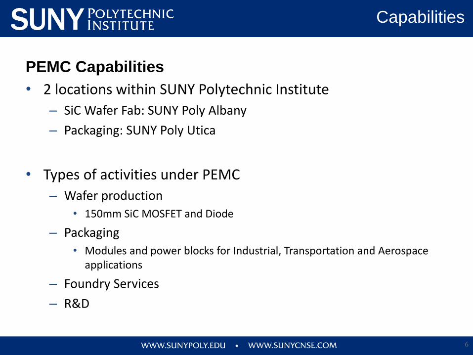
PEMC Capabilities
• 2 locations within SUNY Polytechnic Institute
– SiC Wafer Fab: SUNY Poly Albany
– Packaging: SUNY Poly Utica
• Types of activities under PEMC
– Wafer production
• 150mm SiC MOSFET and Diode
– Packaging
• Modules and power blocks for Industrial, Transportation and Aerospace applications
– Foundry Services
– R&D
6
Capabilities
Phase 1 -- SiC wafer fab
located at SUNY Poly
Albany:
Production capabilities yielding between ~10,000-15,000 wafers/year
MOSFETs initially with Diodes added later
Integrated team of SUNY Poly and GE engineers installing and running the Consortium’s 6” SiC line
Expected on-line by 2Q17
SUNY Poly Albany
PEMC NanoFab 300 North
ZEN Building
NanoFab East
NanoFab 300/450 Extension
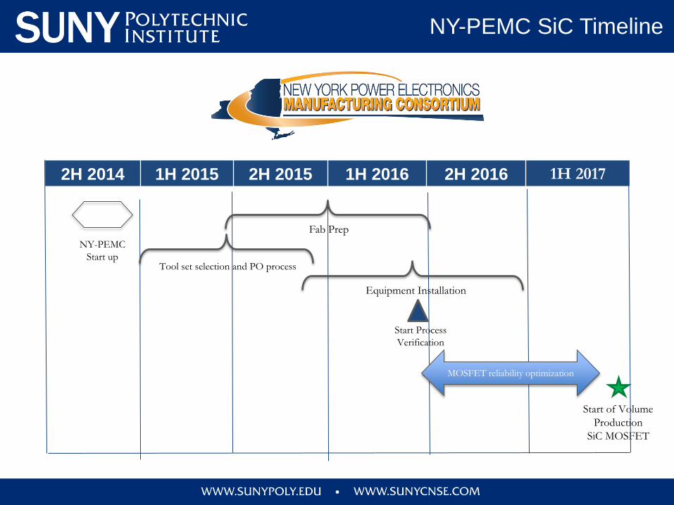
NY-PEMC SiC Timeline
2H 2014 1H 2015 2H 2015 1H 2016 2H 2016 1H 2017
Start of Volume
Production
SiC MOSFET
Equipment Installation
Start Process
Verification
MOSFET reliability optimization
Tool set selection and PO process
Fab Prep
NY-PEMC
Start up

9
February, 2016
PEMC SiC Wafer Line:
SiC dedicated 200mm tools capable of processing 150mm wafers
Class 100 Cleanroom with proper ESD controls
MES managed processing facility under ISO 9001 Quality system
Full complement of metrology and analytical equipment
SiC Fab
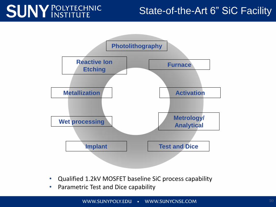
Reactive Ion
Etching
Metallization
Wet processing
Photolithography
Furnace
Metrology/
Analytical
Activation
Implant Test and Dice
• Qualified 1.2kV MOSFET baseline SiC process capability • Parametric Test and Dice capability
10
State-of-the-Art 6” SiC Facility
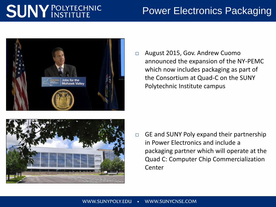
Power Electronics Packaging
August 2015, Gov. Andrew Cuomo announced the expansion of the NY-PEMC which now includes packaging as part of the Consortium at Quad-C on the SUNY Polytechnic Institute campus
GE and SUNY Poly expand their partnership in Power Electronics and include a packaging partner which will operate at the Quad C: Computer Chip Commercialization Center
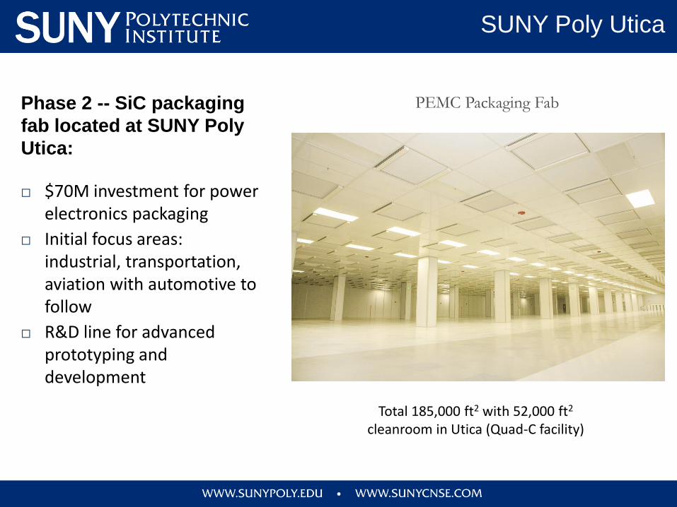
Phase 2 -- SiC packaging
fab located at SUNY Poly
Utica:
$70M investment for power electronics packaging
Initial focus areas: industrial, transportation, aviation with automotive to follow
R&D line for advanced prototyping and development
PEMC Packaging Fab
Total 185,000 ft2 with 52,000 ft2 cleanroom in Utica (Quad-C facility)
SUNY Poly Utica

Higher max. temperature:
TSiC ≥ 200oC vs. TSi ≤ 150o
Reduced power losses…
by more than 50%
2X higher power density… more
compact / powerful
More reliable in high
temperature environments
SiC Power Electronics

14
Advantages of SiC
Datasheet MOSFET Performance : Room Temperature
Advantages of SiC power MOS technology over traditional Si
SiC
Si
1
10
Power Density
Temperature Frequency
2500C
1500C 10KHz 100KHz

15
SiC Materials and Devices
Product Focused Metrics: 1.2kV and 2.5kV GE’ MOSFET Technology
* Losee et al., ICSCRM 2015,
Giardini Naxos Italy
*
Driving to Low ON-resistance and High Temperature performance with SiC
All data courtesy of PEMC Founding Member General Electric

16
Historical SiC MOS Reliability
Gate stress testing versus time over
process evolution
Small MOS capacitors:
Area: 200 m200 m, tox: 47 nm
ICSCRM 2015, Giardini Naxos Italy
All data courtesy of PEMC Founding Member General Electric
Yu et al., Rutgers/GE,
May 2010
Historical improvement of SiC MOS quality and reliability

17
SiC MOS Reliability
Gate Reliability of Full MOSFETs Lifetime model based on accelerated stress testing
• Lifetime: 𝑇𝐿𝐼𝐹𝐸,63% = 𝑒𝛼0+𝛼1×𝐸𝐹𝐼𝐸𝐿𝐷+𝛼2/𝑘𝑇
• 𝑇𝐿𝐼𝐹𝐸,63% relates stress test to use conditions
• Acceleration factor: 𝐴𝐹 =𝑇𝐿𝐼𝐹𝐸,63% @ 𝑢𝑠𝑒 𝑐𝑜𝑛𝑑𝑖𝑡𝑖𝑜𝑛𝑠
𝑇𝐿𝐼𝐹𝐸,63% @ 𝑡𝑒𝑠𝑡 𝑐𝑜𝑛𝑑𝑖𝑡𝑖𝑜𝑛𝑠
• Model predicts MOSFET intrinsic life >30 years
Gate reliability studied and accurate Lifetime models extracted
1.2kV, 30A (10mm2) MOSFETs
All data courtesy of PEMC Founding Member General Electric
18
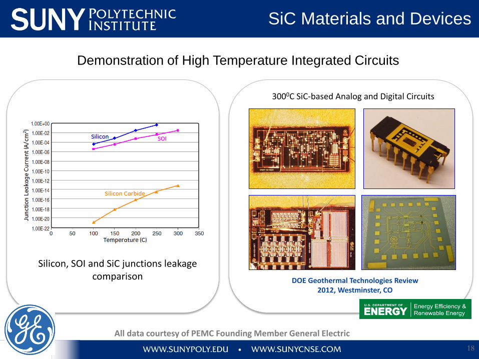
SiC Materials and Devices
Silicon, SOI and SiC junctions leakage comparison
3000C SiC-based Analog and Digital Circuits
DOE Geothermal Technologies Review 2012, Westminster, CO
Demonstration of High Temperature Integrated Circuits
All data courtesy of PEMC Founding Member General Electric

19
Emerging SiC Electronics
• High Density and High Frequency Power
• High Temperature Electronics
• Efficient, Heat Sink Cooled Systems
• Radiation Hard Optimized Electronics
Electric Propulsion Power Systems
Advanced SiC Device Manufacturing and Packaging:
High Temperature Power Systems and Electronics
Advanced Thermal Management

Questions &
Discussion
20
Data Center Products
System
Increasing TRL / MRL 4-7
HVDC / MVDC
MV Motor Drive
PV Inverter
Wind Converter
Data Center
Aviation
EV Charger
DC-DC
600V
10kV
3.3kV
1.2kV
20V


