
Nanoscale Optics and PhotonicsXiaodong Yang, October 25, 2011
The iridescence of Morpho butterfly
• Photonic crystals
• Surface plasmons
• Metamaterials
Reference pictures resources: internet

The scale of things

The electromagnetic spectrum

Vacuum tube
Transistor
Electronic integrated circuits
Early electronics
Geometrical optics
Optical MEMS
Nanophotonicintegrated circuits
Nanofabrication and nanomanufacturing
techniques
Fast, low-cost, scalable and functional integrated devices
Electronics and photonics roadmaps

Photonic crystals in nature
λ/2
Morpho butterfly Peacock feather Sea Mouse hair
Natural opals

Photonic crystal: periodically structured electromagnetic media, generally possessing photonic band gaps. Lattice constants are comparable to the wavelength of light in the material.
Photonic crystals and defects
Point defect: cavity
Line defect: waveguide
λ/2

Photonic crystals with different dimensions

Surface Plasmons
Gothic stained glass rose window of Notre-Dame de Paris

Water surface wave

λSP<<λ0
εd
εm|Ez|
Evanescent field
• Strong light localization near the metal-dielectric interface
• Surface Plasmons with large k
• SP wave interference
Surface Plasmons at metal-dielectric interface
10 µm

Atomic lattice constant a ~ 5.65 Å
Optical wavelength λ ~1μm
Homogeneous medium
Crystal structure of sodium chloride (NaCl)
Natural materials“atoms”
λaa l
Metamaterials
a
Artificially fabricated structures
Unit cell a << wavelength λ
Effective-media theory can be applied
Material properties not existing in natural
materials
“meta-atoms”
Metamaterials: beyond natural materials
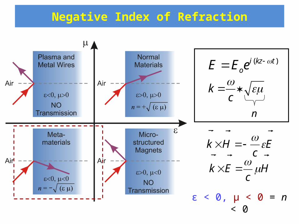
ε < 0, µ < 0 = n < 0
( )i kz toE E e
kc
n
Hc
Ek
Ec
Hk
Negative Index of Refraction

Negative Index of Refraction
Snell’s Law

Photonic integrated circuits
• Photonic crystals
• Surface plasmons
• Metamaterials

Renewable energy • Solar energy harvesting• Thin-film photovoltaics• LED lighting
Optical communications• Photonic crystal fibers• Photodetectors• Optical switches
Industrial applications• Photolithography• Laser manufacturing• High-power fiber lasers
Consumer electronics• Semiconductor lasers• CCD imaging• LCD and LED displays
Biomedical• Biosensors• Fluorescence imaging• Cancer therapy
Nanoscale Optics and Photonics
Applications of nanoscale optics and photonics


