
Nano Spider - ORG4400 Evaluation Kit Datasheet Revision 1.0 Page 1 of 21
November 23, 2014
NANO HORNET (ORG1411)
EVALUATION KIT
Datasheet
O r i g i n G P S . c o m

Page 2 of 14 June 25, 2015
Nano Hornet - ORG1411 Evaluation Kit Datasheet Revision 2.0
INDEX 1. SCOPE ...................................................................................................................................................... 4 2. DISCLAIMER ............................................................................................................................................ 4 3. SAFETY INFORMATION ............................................................................................................................ 4 4. ESD SENSITIVITY ...................................................................................................................................... 4 5. CONTACT INFORMATION ........................................................................................................................ 4 6. RELATED DOCUMENTATION ................................................................................................................... 4 7. REVISION HISTORY .................................................................................................................................. 5 8. ABOUT HORNET FAMILY ........................................................................................................................ 5 9. ABOUT NANO HORNET MODULE …………................................................................................................ 5 10. ABOUT ORIGINGPS .................................................................................................................................. 6 11. DESCRIPTION ........................................................................................................................................... 6 12. SCHEMATICS ........................................................................................................................................... 7 12.1. MAIN BOARD SCHEMATICS ..................................................................................................................... 7 12.2. INTERFACE ADAPTOR SCHEMATICS ........................................................................................................ 8 13. BILL OF MATERIALS ................................................................................................................................. 9 13.1. MAIN BOARD BILL OF MATERIALS .......................................................................................................... 9 13.2. INTERFACE ADAPTOR BILL OF MATERIALS .............................................................................................. 9 14. ASSEMBLY AND LAYOUT ......................................................................................................................... 10 14.1. MAIN BOARD PCB ................................................................................................................................... 10 14.2. INTERFACE ADAPTOR PCB ....................................................................................................................... 12 15. TTL-232R-3V3 USB-Serial CONVERTER CABLE ......................................................................................... 15
TABLE INDEX TABLE 1 – RELATED DOCUMENTATION.................................................................................................................. 4 TABLE 2 – REVISION HISTORY................................................................................................................................. 5 TABLE 3 – MAIN BOARD BILL OF MATERIALS ......................................................................................................... 9 TABLE 4 – INTERFACE ADAPTOR BILL OF MATERIALS ............................................................................................ 9 TABLE 5 – USB-SERIAL CONVERTER CABLE HEADER PIN-OUT ............................................................................. 15 TABLE 6 – USB-SERIAL CONVERTER CABLE OPERATING PARAMETERS .............................................................. 15

Page 3 of 14 June 25, 2015
Nano Hornet - ORG1411 Evaluation Kit Datasheet Revision 2.0
FIGURE INDEX FIGURE 1 – MAIN BOARD SCHEMATICS ................................................................................................................. 7 FIGURE 2 – INTERFACE ADAPTOR SCHEMATICS..................................................................................................... 8 FIGURE 3 – MAIN BOARD COMPONENTS PLACEMENT ........................................................................................ 10 FIGURE 4 – MAIN BOARD SOLDER MASK ............................................................................................................. 10 FIGURE 5 – MAIN BOARD TOP LAYER ROUTING .................................................................................................. 11 FIGURE 6 – MAIN BOARD BOTTOM LAYER ROUTING ........................................................................................... 11 FIGURE 7 – INTERFACE ADAPTOR BOARD COMPONENTS PLACEMENT .............................................................. 12 FIGURE 8 – INTERFACE ADAPTOR BOARD SOLDER MASK .................................................................................... 12 FIGURE 9 – INTERFACE ADAPTOR BOARD TOP LAYER ROUTING ......................................................................... 13 FIGURE 10 – INTERFACE ADAPTOR INNER LAYER 1 ROUTING ............................................................................. 13 FIGURE 11 – INTERFACE ADAPTOR INNER LAYER 2 ROUTING ............................................................................. 14 FIGURE 12 – INTERFACE ADAPTOR BOTTOM LAYER ROUTING............................................................................ 14 FIGURE 13 – PIN HEADER SOCKET BOTTOM VIEW .............................................................................................. 15

Page 4 of 14 June 25, 2015
Nano Hornet - ORG1411 Evaluation Kit Datasheet Revision 2.0
1. SCOPE
This document describes the features and specifications of Nano Hornet ORG1411 evaluation kit.
2. DISCLAIMER
All trademarks are properties of their respective owners. Performance characteristics listed in this document do not constitute a warranty or guarantee of product performance. OriginGPS assumes no liability or responsibility for any claims or damages arising out of the use of this document, or from the use of integrated circuits based on this document. OriginGPS assumes no liability or responsibility for unintentional inaccuracies or omissions in this document. OriginGPS reserves the right to make changes in its products, specifications and other information at any time without notice. OriginGPS reserves the right to conduct, from time to time, and at its sole discretion, firmware upgrades. As long as those FW improvements have no material change on end customers, PCN may not be issued. OriginGPS navigation products are not recommended to use in life saving or life sustaining applications.
3. SAFETY INFORMATION
Improper handling and use can cause permanent damage to the product.
4. ESD SENSITIVITY
This product is ESD sensitive device and must be handled with care.
5. CONTACT INFORMATION
Support - [email protected] or Online Form
Marketing and sales - [email protected]
Web – www.origingps.com
6. RELATED DOCUMENTATION
DOCUMENT NAME
1 Nano Hornet – ORG1411 Datasheet
2 Spider and Hornet - NMEA Protocol Reference Manual
3 Spider and Hornet - OSP® Reference Manual
4 Spider and Hornet - OSP® GNSS Extensions Reference Manual
5 Spider and Hornet - Low Power Modes Application Note
6 Spider and Hornet - Client Generated Extended Ephemeris Application Note
7 Spider and Hornet - Server Generated Extended Ephemeris Application Note
8 Spider and Hornet - Ephemeris Push Application Note
TABLE 1 – RELATED DOCUMENTATION
Page 5 of 14 June 25, 2015
Nano Hornet - ORG1411 Evaluation Kit Datasheet Revision 2.0
7. REVISION HISTORY
REVISION DATE CHANGE DESCRIPTION
A01 May 1, 2012 First release
2.0 June 25, 2015 Format Update
TABLE 2 – REVISION HISTORY
8. ABOUT HORNET FAMILY
OriginGPS GNSS receiver modules have been designed to address markets where size, weight, stand-alone operation, highest level of integration, power consumption and design flexibility - all are very important.
OriginGPS’ Hornet family breaks size barrier, offering the industry’s smallest fully-integrated, highly-sensitive GPS and GNSS modules with integrated antennas or on-board RF connectors.
Hornet family features OriginGPS' proprietary NFZ™ technology for high sensitivity and noise immunity even under marginal signal condition, commonly found in urban canyons, under dense foliage or when the receiver’s position in space rapidly changes.
Hornet family enables the shortest TTM (Time-To-Market) with minimal design risks.
Just connect power supply on a single layer PCB.
9. ABOUT NANO HORNET MODULE
Nano Hornet is a complete SiP featuring miniature LGA SMT footprint designed to commit unique integration features for high volume cost sensitive applications, sharing same footprint, electrical interface and software with OriginGPS’ Micro Hornet ORG1411 module in ultimate ultra-low profile of 3.8mm.
Designed to support space constrained applications such as smart watches, action cameras and wearable devices, Nano Hornet ORG1411 module is an ultra-compact, ultra-low profile and ultra-low weight multi-channel GPS with SBAS, QZSS and other regional overlay systems receiver that continuously tracks all satellites in view, providing real-time positioning data in industry’s standard NMEA format.
Nano Hornet ORG1411 module offers superior sensitivity and outstanding performance, achieving rapid TTFF in less than one second, accuracy of approximately two meters, and tracking sensitivity of -163dBm.
Sized only 10mm x 10mm Nano Hornet ORG1411 module is industry’s small sized, record breaking solution.
Nano Hornet module integrates OriginGPS proprietary low profile GPS antenna, dual-stage LNA, RF LDO, SAW filter, TCXO, RTC crystal and RF shield with market-leading SiRFstarIV™ GPS SoC.
Nano Hornet ORG1411 module is introducing industry’s lowest energy per fix ratio, unparalleled accuracy and extremely fast fixes even under challenging signal conditions, such as in built-up urban areas, dense foliage or even indoor.
Integrated GPS SoC incorporating high-performance microprocessor and sophisticated firmware keeps positioning payload off the host, allowing integration in embedded solutions with low computing resources.
Innovative architecture can detect changes in context, temperature, and satellite signals to achieve a state of near continuous availability by maintaining and opportunistically updating its internal fine time, frequency, and satellite ephemeris data while consuming mere microwatts of battery power.

Page 6 of 14 June 25, 2015
Nano Hornet - ORG1411 Evaluation Kit Datasheet Revision 2.0
10. ABOUT ORIGINGPS
OriginGPS is a world leading designer, manufacturer and supplier of miniature positioning modules, antenna modules and antenna solutions. OriginGPS modules introduce unparalleled sensitivity and noise immunity by incorporating Noise Free Zone system (NFZ™) proprietary technology for faster position fix and navigation stability even under challenging satellite signal conditions. Founded in 2006, OriginGPS is specializing in development of unique technologies that miniaturize RF modules, thereby addressing the market need for smaller wireless solutions.
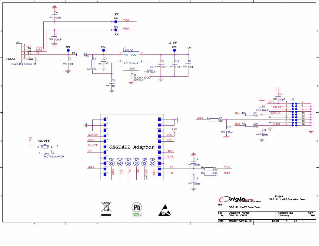
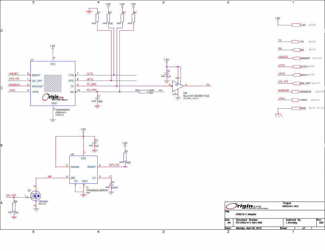
11. DESCRIPTION Evaluation Kit of the ORG1411 GPS Antenna Module comprises the Demo Board, USB to UART cable and CD with GPS simulator software for PC and documentation. The Demo Board is built of Main Board, incorporating 1.8V LDO regulator, UART connector, push-button tactile switch for Push-To-Fix™ interrupt and various test points. The ORG1411 GPS Antenna Module is soldered onto the Main Board through the Interface Adaptor. The Interface Adaptor includes a single-bit buffer for voltage level translation of TX line, and a voltage supervisor for autonomous power-on pulse generation.
5
5
4
4
3
3
2
2
1
1
D D
C C
B B
A A
Black GND
5VRXTX
RX
TX
ON/OFF
1.8V
ORG1411 Adaptor
5V
GPIO13
ON_OFF
1PPS
GPIO1
RSTN
RxDATxDA
RxDA
TxDA
NC1
TxDA
RxDA
1PPS
ON_OFF
RSTN
VCCWAKEUP
nCTS
nRTS
TX
RX
NC2
NC1
NC2
TX
RX
ON
_O
FF
1P
PS
GN
D
VC
C
1.8V
1.8V
1.8V
Title
Size Document Number Rev
Date: Sheet o f
Authored By:
Project
ORG1411-DBUA A00
ORG1411 UART Demo Board
A4
1 1Monday, April 30, 2012
I. Divinsky
ORG1411 UART Evaluation Board
Title
Size Document Number Rev
Date: Sheet o f
Authored By:
Project
ORG1411-DBUA A00
ORG1411 UART Demo Board
A4
1 1Monday, April 30, 2012
I. Divinsky
ORG1411 UART Evaluation Board
Title
Size Document Number Rev
Date: Sheet o f
Authored By:
Project
ORG1411-DBUA A00
ORG1411 UART Demo Board
A4
1 1Monday, April 30, 2012
I. Divinsky
ORG1411 UART Evaluation Board
TP3
PAD20
TP2
PAD3
C10
100pF0402
PAD10
C5
1uF0603
R3 33R
0402
PAD17
R7 33R
0402
PIN1
C15
100pF0402
C14
100pF0402
C4
100pF0402
PIN3
PAD1
J21 23
456
7 89 10
11 1213 1415 1617 18
R2
100K0402
PAD18
TP1
case
SW1TACTILE SWITCH
1 3
42
R6 33R
0402
C8
0402 18pF
R5 33R
0402
J1
HEADER 6 2.54mm RA
123456
PAD7
C7
4.7uF0805C6
10nF0402
PIN5
PAD14
PAD4
PAD12
C1
100pF0402
R1 1R
0402
C3
1uF0603
PAD16
PIN6
PAD22
C12
100pF0402
C13
4.7uF0805
PAD2
PAD11
PAD19
TP5
PAD15
C9
100pF0402
PIN2
C2
18pF0402
R4 33R
0402
PIN4
C11
100pF0402PAD8
PAD5
U11.8V LDO
TLV70018DDCTSOT23-5
TI
VIN1
GND
2
EN3
NR/ADJ4
VOUT5
PAD9
PAD21
PAD6
PAD13
TP4
5
5
4
4
3
3
2
2
1
1
D D
C C
B B
A A
(pin5)
(pin8)
(pin15)
(pin17)
(pin2)
(pin1)
(pin16)
(pin21)
(pins 10-14)
(pin4)
GPS_ON
WAKEUP TX
nRESET
1PPS RX_GPS
CT
ON_OFF
GPS_ON
MR
TX_GPS
TX
ON_OFF
1PPS
WAKEUP
RX
nRTS
nRESET
nCTS
RX
nRTS
nCTSnRTS
WAKEUP
ON_OFF
1PPS
GND
1.8V
TX
RX
nCTS
nRESET
1.8V
1.8V
1.8V
1.8V
1.8V
1.8V1.8V 1.8V
Title
Size Document Number Rev
Date: Sheet o f
Authored By:
Project
PD-ORG1411-AD1-A00 A00
ORG1411 Adaptor
A4
1 1Monday, April 30, 2012
I. Divinsky
ORG1411-AD1
Title
Size Document Number Rev
Date: Sheet o f
Authored By:
Project
PD-ORG1411-AD1-A00 A00
ORG1411 Adaptor
A4
1 1Monday, April 30, 2012
I. Divinsky
ORG1411-AD1
Title
Size Document Number Rev
Date: Sheet o f
Authored By:
Project
PD-ORG1411-AD1-A00 A00
ORG1411 Adaptor
A4
1 1Monday, April 30, 2012
I. Divinsky
ORG1411-AD1
R7
100K0402
R4
0402
R1
0402
C1
18pF0402
U3
DRV
TITPS3808G18DRVR
SENSE2
VDD
1
RESET6
MR4
GND
5
CT3
EP
7
R5 100R0402
C4
100nF0402
C2
1uF0402
R2
0402 10K
R3
0402
R6
10K0402
U2
ON
ULLGA6_1.0x1.0NLU1GT126CMX1TCG
2 4
5 316
U1
ORIGINGPS
LGA1010ORG1411
TX3
RX10
VCC
4
GND
5
RESET8
ON_OFF1
WAKEUP6
1PPS2
CTS7
RTS9
Q1
2N7002SOT-23
1
32
C3
1uF0402

Page 9 of 15 June 25, 2015
Nano Hornet - ORG1411 Evaluation Kit Datasheet
Revision 2.0
13. BILL OF MATERIALS
13.1 MAIN BOARD BILL OF MATERIALS
Reference Value Description P/N MFG
C2, C8 18pF CAP SMT 0402 18pF ±5% 50V COG GRM1555C1H180JZ01D MURATA
C1,C4, C9, C10, C11, C12, C14, C15
100pF
CAP SMT 0402 100pF ±5% 50V COG
GRM1555C1H101JA01D
MURATA
C6 10nF CAP SMT 0402 10nF ±10% 25V X7R GRM155R71E103KA01D MURATA
C3, C5 1µF CAP SMT 0603 1µF ±10% 10V X5R GRM188R60J105KA01J MURATA
C7, C13 4.7µF CAP SMT 0805 4.7µF ±10% 16V X5R GRM21BR61C475KA88L MURATA
R1 1Ω RES SMT 0402 1Ω ±1% RM04FTN0010 TA-I
R3, R4, R5, R6, R7 33Ω RES SMT 0402 33Ω ±1% RM04FTN0330 TA-I
R2 100KΩ RES SMT 0402 100KΩ ±1% RM04FTN1003 TA-I
J1 HDR HEADER 6 POS. 0.1“ RIGHT ANGLE 2211S-06G-F1 NELTRON
SW1 TSW TACT SWITCH SMT KSC222JLFS C&K
U1 LDO LDO REG. SMT SOT23-5 3.3V 200mA TLV70033DDCT TI
TABLE 3 - MAIN BOARD BILL OF MATERIALS
13.2 INTERFACE ADAPTOR BILL OF MATERIALS
Reference Value Description P/N MFG
C1 18pF CAP SMT 0402 18pF ±5% 50V COG GRM1555C1H180JZ01D MURATA
C4 100nF CAP SMT 0402 100nF ±10% 16V X7R GRM155R71C104KA88D MURATA
C2,C3 1µF CAP SMT 0402 1µF ±10% 10V X5R GRM155R61A105KE15D MURATA
R5 100Ω RES SMT 0402 100Ω ±1% RM04FTN1000 TA-I
R2,R6 10KΩ RES SMT 0402 10KΩ ±1% RM04FTN1002 TA-I
R7 100KΩ RES SMT 0402 100KΩ ±1% RM04FTN1003 TA-I
Q1 2N7002 N-CH MOSFET SOT-23 2N7002KT1G ON
U1 MODULE GPS ANTENNA MODULE SMT LGA ORG1411 ORIGINGPS
U2 NLU1GT126 SINGLE BUFFER 3-STATE NLU1GT126CMX1TCG ON
U3 TPS3808 LOW IQ POR SUPERVISOR W. MAN. RST TPS3808G18DRVR TI
TABLE 4 - INTERFACE ADAPTOR BILL OF MATERIALS

Page 10 of 15 June 25, 2015
Nano Hornet - ORG1411 Evaluation Kit Datasheet
Revision 2.0
14. ASSEMBLY AND LAYOUT 14.1 MAIN BOARD PCB
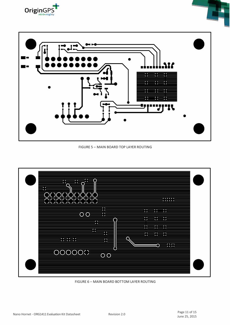
Main Board for the ORG1411 GPS Antenna Module is 2 layers 1.6mm thickness FR4 PCB.
FIGURE 3 - MAIN BOARD COMPONENTS PLACEMENT
FIGURE 4 - MAIN BOARD SOLDER MASK
Page 11 of 15 June 25, 2015
Nano Hornet - ORG1411 Evaluation Kit Datasheet
Revision 2.0
FIGURE 5 – MAIN BOARD TOP LAYER ROUTING
FIGURE 6 – MAIN BOARD BOTTOM LAYER ROUTING

Page 12 of 15 June 25, 2015
Nano Hornet - ORG1411 Evaluation Kit Datasheet
Revision 2.0
14.2 INTERFACE ADAPTOR PCB Interface Adaptor Board for the ORG1411 GPS Antenna Module is 17mm x 17mm 22 pads 4 layers 0.6mm
thickness FR4 PCB.
FIGURE 7 - INTERFACE ADAPTOR BOARD COMPONENTS PLACEMENT
FIGURE 8 - INTERFACE ADAPTOR BOARD SOLDER MASK

Page 13 of 15 June 25, 2015
Nano Hornet - ORG1411 Evaluation Kit Datasheet
Revision 2.0
FIGURE 9 - INTERFACE ADAPTOR BOARD TOP LAYER ROUTING
FIGURE 10 - INTERFACE ADAPTOR INNER LAYER 1 ROUTING
Page 14 of 15 June 25, 2015
Nano Hornet - ORG1411 Evaluation Kit Datasheet
Revision 2.0
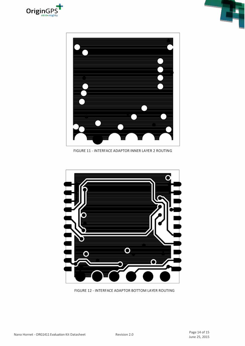
FIGURE 11 - INTERFACE ADAPTOR INNER LAYER 2 ROUTING
FIGURE 12 - INTERFACE ADAPTOR BOTTOM LAYER ROUTING
Page 15 of 15 June 25, 2015
Nano Hornet - ORG1411 Evaluation Kit Datasheet
Revision 2.0
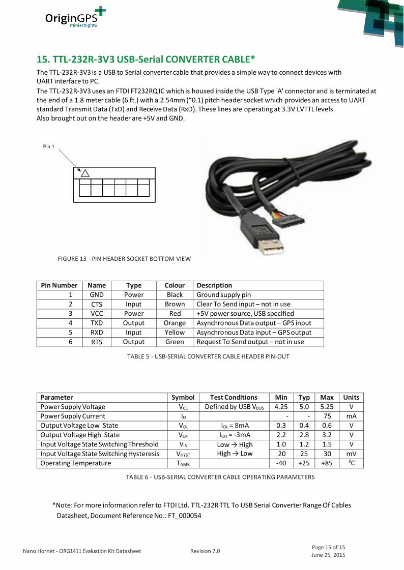
15. TTL-232R-3V3 USB-Serial CONVERTER CABLE* The TTL-232R-3V3 is a USB to Serial converter cable that provides a simple way to connect devices with UART interface to PC.
The TTL-232R-3V3 uses an FTDI FT232RQ IC which is housed inside the USB Type 'A' connector and is terminated at the end of a 1.8 meter cable (6 ft.) with a 2.54mm (“0.1) pitch header socket which provides an access to UART standard Transmit Data (TxD) and Receive Data (RxD). These lines are operating at 3.3V LVTTL levels. Also brought out on the header are +5V and GND.
FIGURE 13 - PIN HEADER SOCKET BOTTOM VIEW
Pin Number Name Type Colour Description 1 GND Power Black Ground supply pin 2 CTS Input Brown Clear To Send input – not in use 3 VCC Power Red +5V power source, USB specified 4 TXD Output Orange Asynchronous Data output – GPS input 5 RXD Input Yellow Asynchronous Data input – GPS output 6 RTS Output Green Request To Send output – not in use
TABLE 5 - USB-SERIAL CONVERTER CABLE HEADER PIN-OUT
Parameter Symbol Test Conditions Min Typ Max Units Power Supply Voltage VCC Defined by USB VBUS 4.25 5.0 5.25 V Power Supply Current IO - - 75 mA Output Voltage Low State VOL IOL = 8mA 0.3 0.4 0.6 V Output Voltage High State VOH IOH = -3mA 2.2 2.8 3.2 V Input Voltage State Switching Threshold VIN Low → High
High → Low
1.0 1.2 1.5 V Input Voltage State Switching Hysteresis VHYST 20 25 30 mV Operating Temperature TAMB -40 +25 +85 0C
TABLE 6 - USB-SERIAL CONVERTER CABLE OPERATING PARAMETERS
*Note: For more information refer to FTDI Ltd. TTL-232R TTL To USB Serial Converter Range Of Cables
Datasheet, Document Reference No.: FT_000054


