Document Number: MPC17510Rev. 6.0, 7/2016
NXP Semiconductors Technical Data
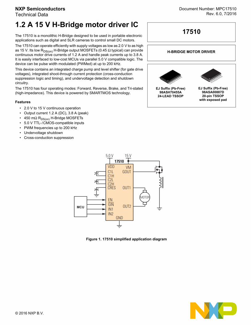
1.2 A 15 V H-Bridge motor driver ICThe 17510 is a monolithic H-Bridge designed to be used in portable electronic applications such as digital and SLR cameras to control small DC motors.
The 17510 can operate efficiently with supply voltages as low as 2.0 V to as high as 15 V. Its low RDS(on) H-Bridge output MOSFETs (0.45 Ω typical) can provide continuous motor drive currents of 1.2 A and handle peak currents up to 3.8 A. It is easily interfaced to low-cost MCUs via parallel 5.0 V compatible logic. The device can be pulse width modulated (PWMed) at up to 200 kHz.
This device contains an integrated charge pump and level shifter (for gate drive voltages), integrated shoot-through current protection (cross-conduction suppression logic and timing), and undervoltage detection and shutdown circuitry.
The 17510 has four operating modes: Forward, Reverse, Brake, and Tri-stated (high-impedance). This device is powered by SMARTMOS technology.
Features
• 2.0 V to 15 V continuous operation • Output current 1.2 A (DC), 3.8 A (peak)• 450 mΩ RDS(on) H-Bridge MOSFETs
• 5.0 V TTL- / CMOS-compatible inputs• PWM frequencies up to 200 kHz • Undervoltage shutdown• Cross-conduction suppression
Figure 1. 17510 simplified application diagram
H-BRIDGE MOTOR DRIVER
EJ Suffix (Pb-Free)98ASH70455A
24-LEAD TSSOP
17510
EJ Suffix (Pb-Free)98ASA00887D20-pin TSSOP
with exposed pad
VDD
CRES
C1LC1HC2LC2H
IN2IN1
EN
OUT2
OUT1
GOUTVM
GND
MCUGIN
MOTOR
5.0 V 15 V17510
© 2016 NXP B.V.
1 Orderable parts
Table 1. Orderable part variations (1)
Part number Temperature (TA) Package
MPC17510AEJ -30 °C to 65 °C
20 TSSOP (exposed pad)
MPC17510EJ (2) 24 TSSOPW
Notes1. To order parts in Tape & Reel, add the R2 suffix to the part number.2. Not recommended for new designs.
2 NXP Semiconductors
17510

2 Internal block diagram
Figure 2. 17510 simplified internal block diagram
Charge Pump
H-BridgeLevelShifter
Predriver
ControlLogic
Low VoltageDetector
GOUT
VM
VM
OUT1
OUT1
OUT2
OUT2
PGND
PGND
CRES
VDD
LGND
GIN
EN
IN2
IN1
C1LC1HC2LC2H
NXP Semiconductors 3
17510
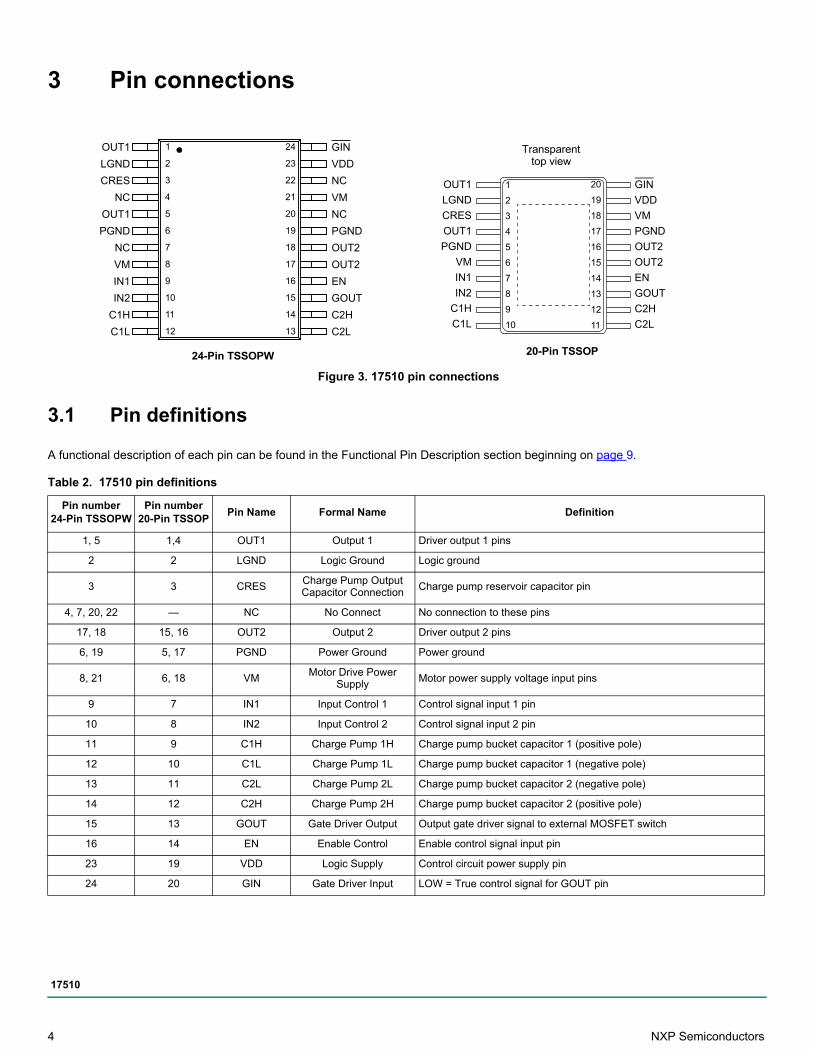
3 Pin connections
Figure 3. 17510 pin connections
3.1 Pin definitions
A functional description of each pin can be found in the Functional Pin Description section beginning on page 9. Table 2. 17510 pin definitions
Pin number24-Pin TSSOPW
Pin number20-Pin TSSOP
Pin Name Formal Name Definition
1, 5 1,4 OUT1 Output 1 Driver output 1 pins
2 2 LGND Logic Ground Logic ground
3 3 CRESCharge Pump Output Capacitor Connection
Charge pump reservoir capacitor pin
4, 7, 20, 22 — NC No Connect No connection to these pins
17, 18 15, 16 OUT2 Output 2 Driver output 2 pins
6, 19 5, 17 PGND Power Ground Power ground
8, 21 6, 18 VMMotor Drive Power
SupplyMotor power supply voltage input pins
9 7 IN1 Input Control 1 Control signal input 1 pin
10 8 IN2 Input Control 2 Control signal input 2 pin
11 9 C1H Charge Pump 1H Charge pump bucket capacitor 1 (positive pole)
12 10 C1L Charge Pump 1L Charge pump bucket capacitor 1 (negative pole)
13 11 C2L Charge Pump 2L Charge pump bucket capacitor 2 (negative pole)
14 12 C2H Charge Pump 2H Charge pump bucket capacitor 2 (positive pole)
15 13 GOUT Gate Driver Output Output gate driver signal to external MOSFET switch
16 14 EN Enable Control Enable control signal input pin
23 19 VDD Logic Supply Control circuit power supply pin
24 20 GIN Gate Driver Input LOW = True control signal for GOUT pin
GIN
NC
PGND
OUT2
OUT2
EN
GOUT
C2H
C2L
VDD
NC
VM
OUT1
OUT1
PGND
NC
VM
IN1
IN2
C1L
LGND
CRES
NC
C1H
24
20
19
18
17
16
15
13
23
22
21
14
5
6
7
8
9
10
11
12
2
3
4
1
24-Pin TSSOPW 20-Pin TSSOP
Transparenttop view
OUT1
LGND
CRES
OUT1
PGND
VM
IN1
IN2
C1H
C1L
GIN
VDD
VM
OUT2
EN
GOUT
C2H
C2L
PGND
OUT2
1
2
3
4
5
6
7
8
9
10
20
19
18
17
16
15
14
13
12
11
4 NXP Semiconductors
17510
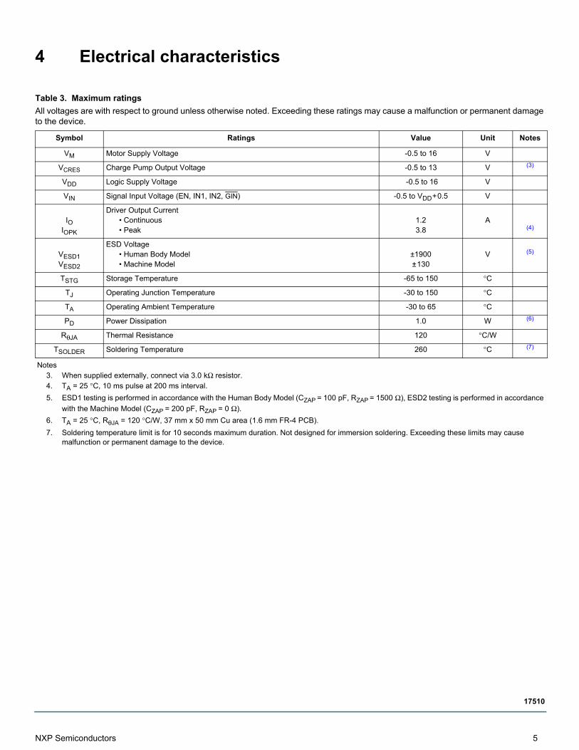
4 Electrical characteristics
Table 3. Maximum ratings All voltages are with respect to ground unless otherwise noted. Exceeding these ratings may cause a malfunction or permanent damage to the device.
Symbol Ratings Value Unit Notes
VM Motor Supply Voltage -0.5 to 16 V
VCRES Charge Pump Output Voltage -0.5 to 13 V (3)
VDD Logic Supply Voltage -0.5 to 16 V
VIN Signal Input Voltage (EN, IN1, IN2, GIN) -0.5 to VDD + 0.5 V
IOIOPK
Driver Output Current• Continuous• Peak
1.23.8
A(4)
VESD1VESD2
ESD Voltage • Human Body Model • Machine Model
±1900± 130
V (5)
TSTG Storage Temperature -65 to 150 °C
TJ Operating Junction Temperature -30 to 150 °C
TA Operating Ambient Temperature -30 to 65 °C
PD Power Dissipation 1.0 W (6)
RθJA Thermal Resistance 120 °C/W
TSOLDER Soldering Temperature 260 °C (7)
Notes3. When supplied externally, connect via 3.0 kΩ resistor.4. TA = 25 °C, 10 ms pulse at 200 ms interval.
5. ESD1 testing is performed in accordance with the Human Body Model (CZAP = 100 pF, RZAP = 1500 Ω), ESD2 testing is performed in accordance
with the Machine Model (CZAP = 200 pF, RZAP = 0 Ω).
6. TA = 25 °C, RθJA = 120 °C/W, 37 mm x 50 mm Cu area (1.6 mm FR-4 PCB).
7. Soldering temperature limit is for 10 seconds maximum duration. Not designed for immersion soldering. Exceeding these limits may cause malfunction or permanent damage to the device.
NXP Semiconductors 5
17510

4.1 Static electrical characteristics
Table 4. Static electrical characteristics
Characteristics noted under conditions TA = 25 °C, VM = 15 V, VDD = 5.0 V, GND = 0 V, unless otherwise noted. Typical values noted reflect the approximate parameter means at TA = 25 °C under nominal conditions, unless otherwise noted.
Symbol Characteristic Min. Typ. Max. Unit Notes
Power
VM Motor Supply Voltage 2.0 – 15 V
VDD Logic Supply Voltage 4.0 – 5.5 V
C1, C2, C3 Capacitor for Charge Pump 0.001 – 0.1 μF
I VMSTBY
I VDDSTBY
Standby Power Supply Current • Motor Supply Standby Current• Logic Supply Standby Current
––
–0.3
1.01.0
μAmA
(8)
I VDD Logic Supply Current – 3.3 4.0 mA (9)
VDDDETVMDET
Low Voltage Detection Circuit• Detection Voltage (VDD)
• Detection Voltage (VM) 1.54.0
2.55.0
3.56.0
V (10)
RDS(on)Driver Output ON Resistance
• VM = 2.0 V, 8.0 V, 15 V – 0.45 0.55W (11)
Gate drive
VCRESGate Drive Voltage
• No Current Load 12 13 13.5V (12)
VCRESLOADGate Drive Ability (Internally Supplied)
• ICRES = -1.0 mA 10 11.2 –V
VGOUTHIGHVGOUTLOW
Gate Drive Output • IOUT = -50 μA
• IIN = 50 μAVCRES - 0.5
LGNDVCRES - 0.1LGND + 0.1
VCRES LGND +0.5
V
Control logic
VIN Logic Input Voltage (EN, IN1, IN2, GIN) 0.0 – VDD V
VIHVILIIHIILIIL
Logic Input Function (4.0 V < VDD < 5.5 V)• High Level Input Voltage • Low Level Input Voltage • High Level Input Current • Low Level Input Current • EN / GIN Pin
VDD x 0.7––
-1.0- 200
––––
- 50
–VDD x 0.3
1.0––
VV
μAμAμA
Notes8. Excluding pull-up resistor current, including current of gate-drive circuit.9. fIN = 100 kHz.
10. Detection voltage is defined as when the output becomes high-impedance after VDD drops below the detection threshold. When the gate voltage
VCRES is applied from an external source, VCRES = 7.5 V.
11. IO = 1.2 A source + sink.
12. Input logic signal not present.
6 NXP Semiconductors
17510

4.2 Dynamic electrical characteristics
4.3 Timing diagrams
Figure 4. tPLH, tPHL, and tPZH timing Figure 5. Low-voltage detection timing
Table 5. Dynamic electrical characteristics
Characteristics noted under conditions TA = 25 °C, VM = 15 V, VDD = 5.0 V, GND = 0 V unless otherwise noted. Typical values noted reflect the approximate parameter means at TA = 25 °C under nominal conditions unless otherwise noted.
Symbol Characteristic Min. Typ. Max. Unit Notes
Input (EN, IN1, IN2, GIN)
fIN Pulse Input Frequency – – 200 kHz
tR Input Pulse Rise Time – – 1.0 (14) μs (13)
tF Input Pulse Fall Time – – 1.0 (14) μs (15)
Output
tPZHtPLHtPHL
Propagation Delay Time• Turn-ON Time• Turn-ON Time• Turn-OFF Time
–––
0.31.20.5
1.02.01.0
μs
tTONtTOFF
GOUT Output Delay Time • Turn-ON Time• Turn-OFF Time
––
––
1010
μs (16)
fOSCtVCRESON
Charge Pump Circuit • Oscillator Frequency• Rise Time
100–
2000.1
4001.0
kHzms (17)
tVDDDET Low-voltage Detection Time – – 10 ms
Notes13. Time is defined between 10% and 90%.14. That is, the input waveform slope must be steeper than this.15. Time is defined between 90% and 10%.16. Load is 500 pF.17. Time to charge CRES to 11 V after application of VDD.
tPZH*,
10%
IN1, IN2, EN
OUTn
50%
90%
tPHL tPLH
* The last state is “Z”.
(GIN)
(GOUT)
(tTON)(tTOFF) tVDDDET
0%
VDD
IM
3.5 V
90%
tVDDDET
VDDDETON VDDDETOFF
(<1.0 μA)
50%
1.5 V
NXP Semiconductors 7
17510
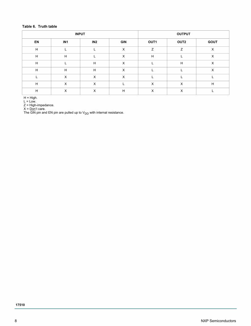
Table 6. Truth table
INPUT OUTPUT
EN IN1 IN2 GIN OUT1 OUT2 GOUT
H L L X Z Z X
H H L X H L X
H L H X L H X
H H H X L L X
L X X X L L L
H X X L X X H
H X X H X X L
H = High. L = Low. Z = High-impedance. X = Don’t care. The GIN pin and EN pin are pulled up to VDD with internal resistance.
8 NXP Semiconductors
17510

5 Functional description
5.1 Introduction
The 17510 is a monolithic H-Bridge power IC applicable to small DC motors used in portable electronics. The 17510 can operate efficiently with supply voltages as low as 2.0 V to as high as 15 V, and it can provide continuos motor drive currents of 1.2 A while handling peak currents up to 3.8 A. It is easily interfaced to low-cost MCUs via parallel 5.0 V-compatible logic. The device can be pulse width modulated (PWM-ed) at up to 200 kHz. The 17510 has four operating modes: Forward, Reverse, Brake, and Tri-stated (High-impedance).
Basic protection and operational features (direction, dynamic braking, PWM control of speed and torque, main power supply undervoltage detection and shutdown, logic power supply undervoltage detection and shutdown), in addition to the 1.0 A rms output current capability, make the 17510 a very attractive, cost-effective solution for controlling a broad range of small DC motors. In addition, a pair of 17510 devices can be used to control bipolar stepper motors. The 17510 can also be used to excite transformer primary windings with a switched square wave to produce secondary winding AC currents.
As shown in Figure 2, 17510 simplified internal block diagram, page 3, the 17510 is a monolithic H-Bridge with built-in charge pump circuitry. For a DC motor to run, the input conditions need to be set as follows: ENable input logic HIGH, one INput logic LOW, and the other INput logic HIGH (to define output polarity). The 17510 can execute dynamic braking by setting both IN1 and IN2 logic HIGH, causing both low-side MOSFETs in the output H-Bridge to turn ON. Dynamic braking can also implemented by taking the ENable logic LOW. The output of the H-Bridge can be set to an open-circuit high-impedance (Z) condition by taking both IN1 and IN2 logic LOW. (refer to Table 6, Truth table, page 8).
The 17510 outputs are capable of providing a continuous DC load current of up to 1.2 A. An internal charge pump supports PWM frequencies to 200 kHz. The EN pin also controls the charge pump, turning it off when EN = LOW, thus allowing the 17510 to be placed in a power-conserving sleep mode.
5.2 Functional pin description
5.2.1 Output 1 and output2 (OUT1, OUT2)The OUT1 and OUT2 pins provide the connection to the internal power MOSFET H-Bridge of the IC. A typical load connected between these pins would be a small DC motor. These outputs will connect to either VM or PGND, depending on the states of the control inputs (refer to Table 6, Truth table, page 8).
5.2.2 Power ground and logic ground (PGND, LGND)The power and logic ground pins (PGND and LGND) should be connected together with a very low-impedance connection.
5.2.3 Charge pump reservoir capacitor (CRES)The CRES pin provides the connection for the external reservoir capacitor (output of the charge pump). Alternatively this pin can also be used as an input to supply gate-drive voltage from an external source via a series current-limiting resistor. The voltage at the CRES pin will be approximately three times the VDD voltage, as the internal charge pump utilizes a voltage tripler circuit. The VCRES voltage is used by the IC to supply gate drive for the internal power MOSFET H-Bridge.
5.2.4 Motor supply voltage input (VM)The VM pins carry the main supply voltage and current into the power sections of the IC. This supply then becomes controlled and/or modulated by the IC as it delivers the power to the load attached between OUT1 and OUT2. All VM pins must be connected together on the printed circuit board with as short as possible traces offering as low impedance as possible between pins.
VM has an undervoltage threshold. If the supply voltage drops below the undervoltage threshold, the output power stage switches to a tri-state condition. When the supply voltage returns to a level that is above the threshold, the power stage automatically resumes normal operation according to the established condition of the input pins.
NXP Semiconductors 9
17510
5.2.5 Control signal input and enable control signal input (IN1, IN2, EN)The IN1, IN2, and EN pins are input control pins used to control the outputs. These pins are 5.0 V CMOS-compatible inputs with hysteresis. The IN1, IN2, and EN work together to control OUT1 and OUT2 (refer to Table 6, Truth table).
5.2.6 Gate driver input (GIN)The GIN input controls the GOUT pin. When GIN is set logic LOW, GOUT supplies a level-shifted high side gate drive signal to an external MOSFET. When GIN is set logic HIGH, GOUT is set to GND potential.
5.2.7 Charge pump bucket capacitor (C1L, C1H, C2L, C2H)These two pairs of pins, the C1L and C1H and the C2L and C2H, connect to the external bucket capacitors required by the internal charge pump. The typical value for the bucket capacitors is 0.1 μF.
5.2.8 Gate driver output (GOUT)The GOUT output pin provides a level-shifted, high side gate drive signal to an external MOSFET with CISS up to 500 pF.
5.2.9 Control circuit power supply (VDD)The VDD pin carries the 5.0 V supply voltage and current into the logic sections of the IC. VDD has an undervoltage threshold. If the supply voltage drops below the undervoltage threshold, the output power stage switches to a tri-state condition. When the supply voltage returns to a level that is above the threshold, the power stage automatically resumes normal operation according to the established condition of the input pins.
10 NXP Semiconductors
17510
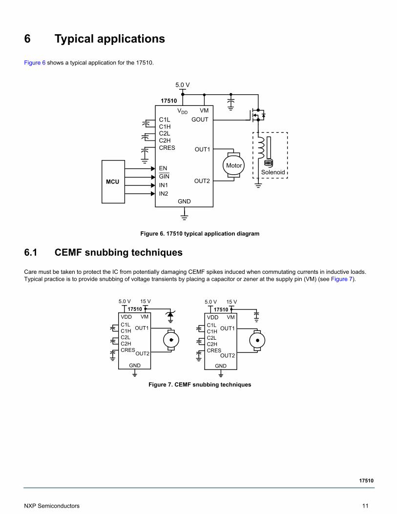
6 Typical applications
Figure 6 shows a typical application for the 17510.
Figure 6. 17510 typical application diagram
6.1 CEMF snubbing techniques
Care must be taken to protect the IC from potentially damaging CEMF spikes induced when commutating currents in inductive loads. Typical practice is to provide snubbing of voltage transients by placing a capacitor or zener at the supply pin (VM) (see Figure 7).
Figure 7. CEMF snubbing techniques
MCU
17510
5.0 V
GND
C1LC1HC2LC2HCRES
EN
GIN
IN1
IN2
VMVDD
Motor
GOUT
Solenoid
OUT1
OUT2
17510
5.0 V 15 V
C1LC1HC2LC2HCRES
VMVDD
OUT1
OUT2
GND
17510
5.0 V 15 V
C1LC1HC2LC2HCRES
VMVDD
OUT1
OUT2
GND
NXP Semiconductors 11
17510

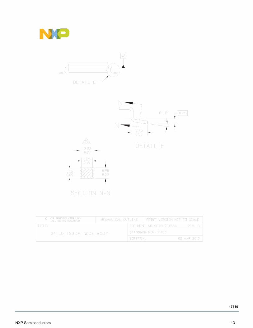
7 Packaging
7.1 Package dimensions
For the most current package revision, visit www.nxp.com and perform a keyword search using the “98A” listed below.
12 NXP Semiconductors
17510
NXP Semiconductors 13
17510

14 NXP Semiconductors
17510

NXP Semiconductors 15
17510

16 NXP Semiconductors
17510

NXP Semiconductors 17
17510

18 NXP Semiconductors
17510

8 Revision history
Revision Date Description of changes
2.0 7/2006• Implemented a Revision History page.• Converted to Freescale format, and updated to the prevailing form and style• Added EJ Pb-FREE package
3.0 1/2007 • Corrected symbol in Table 3, Driver Output ON Resistance from “W” to “Ω”
4.0 11/2013• Corrected pin names to match throughout the document• Corrected minor errors in format. No change in technical content• Moved data sheet to Technical Data status
5.07/2015
• Added 98ASA00887D package information and updated tables where applicable• Added MPC17510AEJ to the ordering information• Updated as per PCN # 16724
8/2015 • Corrected the 98A package information for 20-pin TSSOP
6.010/2015
• Added EP notation for TSSOP package• Fixed notations for TSSOP in Orderable parts and Pin connections• Updated Packaging 98A drawing for TSSOP• Removed MPC17510MTB parts from the data sheet. No longer manufactured.
7/2016 • Updated to NXP document form and style
NXP Semiconductors 19
17510

Information in this document is provided solely to enable system and software implementers to use NXP products.
There are no expressed or implied copyright licenses granted hereunder to design or fabricate any integrated circuits
based on the information in this document. NXP reserves the right to make changes without further notice to any
products herein.
NXP makes no warranty, representation, or guarantee regarding the suitability of its products for any particular
purpose, nor does NXP assume any liability arising out of the application or use of any product or circuit, and
specifically disclaims any and all liability, including without limitation, consequential or incidental damages. "Typical"
parameters that may be provided in NXP data sheets and/or specifications can and do vary in different applications,
and actual performance may vary over time. All operating parameters, including "typicals," must be validated for each
customer application by the customer's technical experts. NXP does not convey any license under its patent rights nor
the rights of others. NXP sells products pursuant to standard terms and conditions of sale, which can be found at the
following address:
http://www.nxp.com/terms-of-use.html.
How to Reach Us:Home Page: NXP.com
Web Support: http://www.nxp.com/support
NXP, the NXP logo, Freescale, the Freescale logo and SMARTMOS are trademarks of NXP B.V. All other product or
service names are the property of their respective owners. All rights reserved.
© 2016 NXP B.V.
Document Number: MPC17510Rev. 6.0
7/2016


