MAHATMA GANDHI UNIVERSITY
SCHEME AND SYLLABIFOR
M. Tech. DEGREE PROGRAMMEIN
ELECTRONICS AND COMMUNICATION ENGINEERING WITH SPECIALIZATION IN
VLSI & EMBEDDED SYSTEM
(2013 ADMISSION ONWARDS)
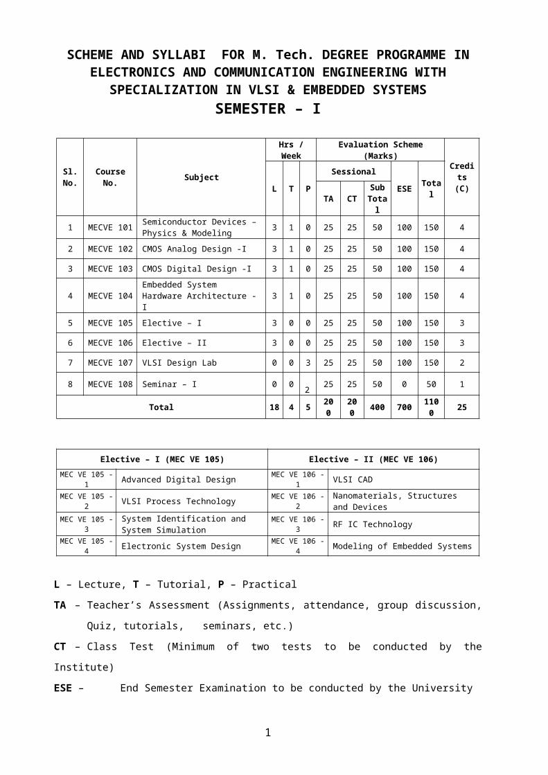
SCHEME AND SYLLABI FOR M. Tech. DEGREE PROGRAMME IN ELECTRONICS AND COMMUNICATION ENGINEERING WITH
SPECIALIZATION IN VLSI & EMBEDDED SYSTEMS SEMESTER – I
Sl. No. Course No. Subject
Hrs / Week Evaluation Scheme (Marks)
Credits (C)L T P
SessionalESE Total
TA CT Sub Total
1 MECVE 101 Semiconductor Devices – Physics & Modeling 3 1 0 25 25 50 100 150 4
2 MECVE 102 CMOS Analog Design -I 3 1 0 25 25 50 100 150 4
3 MECVE 103 CMOS Digital Design -I 3 1 0 25 25 50 100 150 4
4 MECVE 104 Embedded System Hardware Architecture -I 3 1 0 25 25 50 100 150 4
5 MECVE 105 Elective – I 3 0 0 25 25 50 100 150 3
6 MECVE 106 Elective – II 3 0 0 25 25 50 100 150 3
7 MECVE 107 VLSI Design Lab 0 0 3 25 25 50 100 150 2
8 MECVE 108 Seminar – I 0 0 2 25 25 50 0 50 1
Total 18 4 5 200 200 400 700 1100 25
Elective – I (MEC VE 105) Elective – II (MEC VE 106)
MEC VE 105 - 1 Advanced Digital Design MEC VE 106 - 1 VLSI CAD
MEC VE 105 - 2 VLSI Process Technology MEC VE 106 - 2 Nanomaterials, Structures and Devices
MEC VE 105 - 3 System Identification and System Simulation MEC VE 106 - 3 RF IC Technology
MEC VE 105 - 4 Electronic System Design MEC VE 106 - 4 Modeling of Embedded Systems
L – Lecture, T – Tutorial, P – Practical
TA – Teacher’s Assessment (Assignments, attendance, group discussion, Quiz, tutorials, seminars,
etc.)
CT – Class Test (Minimum of two tests to be conducted by the Institute)
ESE – End Semester Examination to be conducted by the University
Electives: New Electives may be added by the department according to the needs of emerging fields of technology. The name of the elective and its syllabus should be submitted to the University before the course is offered.
1

MECVE 101SEMICONDUCTOR DEVICE PHYSICS AND
MODELLING
L T P C3 1 0 4
Module 1
Semiconductors Fundamentals, Mosfet Overview and MOS Capacitor: Semiconductors:
Intrinsic Semiconductors, Free Electrons, and Holes, Extrinsic Semiconductors, Equilibrium in
the Absence of Electric Field, Equilibrium in the Presence of Electric Field, Nonequilibrium;
Quasi-Fermi Levels, Relations between Charge Density, Electric Field, and Potentials; Poisson's
Equation. Conduction: Transit Time, Drift, Diffusion, Total Current. Contact Potentials,
The pn Junction: Overview of the MOS Transistor: Basic Structure, A Qualitative Description
of MOS Transistor Operation, MOS Transistor Characteristics. The Mos Capacitor: The
Flatband Voltage, Potential Balance and Charge Balance, Effect of Gate-Body Voltage on
Surface Condition: Flatband Condition, Accumulation, Depletion, Analysis, Inversion: General
Relations and Regions of Inversion, Strong Inversion, Weak Inversion, Moderate Inversion
Module 2
The Three-Terminal Mos Structure: Contacting the Inversion Layer, The Body Effect,
Regions of Inversion: Approximate Limits, Strong Inversion, Weak Inversion, Moderate
Inversion, A "Vnullnull Control" Point of View: Fundamentals, The "Pinchoff” Voltage
The Four-Terminal Mos Transistor: Transistor Regions of Operation, Complete All-Region
Model, Simplified All-Region Models: Linearizing the Depletion Region Charge, Body-
Referenced Simplified All-Region Models, Source-Referenced Simplified All-Region Models,
Charge Formulation of Simplified All-Region Models
Models Based on Quasi-Fermi Potentials, Regions of Inversion in Terms of Terminal
Voltages: Strong Inversion: Complete Strong-Inversion Model, Body-Referenced Simplified
Strong-Inversion Model, Source-Referenced Simplified Strong-Inversion Model
Moderate-Inversion and Single-Piece Models, Source-Referenced vs. Body-Referenced
Modeling, Effective Mobility, Effect of Extrinsic Source and Drain Series Resistances,
Temperature Effects, Breakdown, The p-Channel MOS Transistor, Enhancement-Mode and
Depletion-Mode Transistors, Model Parameter Values, Model Accuracy, and Model
Comparison
Module 3
Small-Channel And Thin Oxide Effects: Carrier Velocity Saturation, Channel Length
Modulation, Charge Sharing: Short-Channel Devices, Narrow-Channel Devices, Limitations of
2

Charge-Sharing Models, Drain-Induced Barrier Lowering, Punchthrough, Hot Carrier Effects;
Impact Ionization. Scaling: Classical Scaling, Modern Scaling
Large-Signal Modeling Of The Mos Transistor In Transient Operation: Quasi-Static
Operation, Evaluation of Intrinsic Chargers in Quasi-Static Operation: Strong Inversion,
Moderate Inversion, Weak Inversion, All-Region Model, Depletion and Accumulation.Transit
Time under DC Conditions, Limitations of the Quasi-Static Model
Non-Quasi-Static Modeling: The Continuity Equation, Non-Quasi-Static Analysis. Extrinsic
Parasitics: Extrinsic Capacitances, Extrinsic Resistance, Temperature Dependence, Simplified
Models
Module 4
Small-Signal Modeling For Low And Medium Frequencies:
Low-Frequency Small-Signal Model for the Intrinsic Part: Small-Signal Model for the Drain-
to-Source Current, Small-Signal Model for the Gate and Body Currents, Complete Low-
Frequency Small-Signal Model for the Intrinsic Part, Strong Inversion, Weak Inversion,
Moderate Inversion, All-Region Models. A Medium-Frequency Small-Signal Model for the
Intrinsic Part: Intrinsic Capacitances. Including the Extrinsic Part
Noise: White Noise, Flicker Noise, Noise in Extrinsic Resistances, Including Noise in Small-
Signal Circuits. All-Region Models
Modeling For Circuit Simulation: Types of Models, Models for Device Analysis and Design,
Device Models for Circuit Simulation, Attributes of Good Compact Models, Model
Formulation: General Consideration and Choices. Common MOSFET Models Available in
Circuit Simulators: BSIM, EKV, PSP, Other Models
References:
1. Yannis Tsividis and Colin McAndrew , “Operation and Modeling of the MOS
Transistor”, 3/e, 2010, OUP
2. T. Ytterdal, Y. Cheng and T. A. Fjeldly , “Device Modeling for Analog and RF CMOS
Circuit Design”, , John Wiley & Sons, 2003
3. Narain Arora , “MOSFET Modeling For VLSI Simulation: Theory And Practice”, ,
World Scientific, 2007
3

MECVE 102CMOS ANALOG IC I
L T P C3 1 0 4
Module 1
Basics of MOSFET modeling, Current Mirrors - Simple CMOS current mirror Sensitivity
analysis - Temperature analysis -Transient response - Cascode current mirror - Wilson current
mirror, Voltage References - Voltage dividers - Current Source Self-Biasing - Advanced voltage
references - band-gap and beta multiplier referenced circuits
Module 2
Single stage amplifiers - Basic configurations: common source - common drain - common gate
circuits, Active Loads, Cascode amplifiers: folded cascode amplifiers, Push-Pull amplifiers,
CMOS Class AB amplifiers
Module 3
Differential amplifiers - Source coupled pair: current source load – CMRR – Matching
considerations, Source cross coupled pair, cascode loads, Wide swing differential amplifiers:
Current differential amplifier – constant transconductance differential amplifier, Output stages :
source follower as an output stage, CMOS Class AB output stages
Module 4
Frequency response of Amplifiers – General Considerations – Miller effect – Association of
Poles with Nodes, Common source, Source followers , Common gate , Cascode stage,
Differential Pair.
Noise - Statistical Characteristics of Noise - Noise Spectrum - Amplitude Distribution -
Correlated and Uncorrelated Sources, Types of Noise - Thermal Noise - Flicker Noise – shot
noise, Representation of Noise in Circuits, Noise in Single-Stage Amplifiers - Common-Source
Stage - Common-Gate Stage - Source Followers - Cascode Stage, Noise in Differential Pairs,
Noise Bandwidth
References:
1. R. Jacob Baker, Harry W Li, David E Boyce, “ CMOS – Circuit Design, Layout, and
Simulation”,3rd Edition, 1998
2. Behzad Razavi , “Design of Analog CMOS Integrated Circuits”, Tata McGraw Hill
2008
4

3. Gray, Hurst, Lewis, Meyer, “Analysis and Design of Analog Integrated Circuits”, 5 th
Edition, Wiely India,2010
4. Philip E Allen, Douglas R Holberg, “CMOS Analog Circuit Design”, International
Student(Second) Edition, First Indian Edition 2010
Co requisite reading: MOSFET modeling in strong inversion - large signal model, low-
frequency small-signal model, high-frequency small-signal model, body effect, effect of
variations in the fabrication process.
5

MECVE 103CMOS DIGITAL DESIGN I
L T P C3 1 0 4
Module 1.
Static CMOS Inverter: DC Characteristics, Beta Ratio Effects, Noise Margin, Pass Transistor
DC Characteristics. Delay Models: Introduction, Definitions, Timing Optimization, Transiet
Response.
RC Delay Model: Effective Resistance, Gate and Diffusion Capacitance, Equivalent RC
Circuits, Transient Response, Elmore Delay, Layout Dependence of Capcitance, Determining
Effective Resistance.
Linear Delay Model: Logical Effort, Parasistic Delay, Delay in a Logic Gate, Drive, Extracting
Logical Effort from Datasheets, Limitations to the Linear Delay Model. Logical Effort of
Paths: Delay in Multistage Logic Networks, Choosing the Best Number of Stages, Example,
Limitations of Logical Effort, Iterative Solutions for Sizing.
Module 2.
Interconnect effects and power analysis:Introduction, Wire Geometry, Intel Metal Stacks
Interconnect Modeling: Resistance, Capacitance, Inductance, Skin Effect, Temperature
Dependence. Interconnect Impact: Delay, Energy, Crosstalk, Inductive Effects, Effective
Resistance and Elmore Delay. Interconnect Engineering: Width, Spacing and Layer, Repeaters,
Crosstalk Control, Low-Swing Signaling, Regenerators, Logical Effort with Wires.
Module 3.
Static and Dynamic circuits: CMOS Inverter: tristate inverter, Other static CMOS logic gates,
static properties(2 input NAND, NOR), Combinational logic circuits. Layout-examples.
Fundamentals of dynamic logic:, Dynamic pass transistor circuits, CMOS circuits, High
performance dynamic circuits-Domino CMOS, Multi Output Domino Logic, Dual-rail Domino
Logic, NP Domino logic(NORA), True-Single-Phase-Clock(TSPC) CMOS logic, Power
dissipation in CMOS circuits. BiCMOS logic gates, static behavior, switching delay. Silicon-
On-Insulator Circuit Design: Floating Body Voltage, SOI Advantages, Disadvantages
Module 4. System design: Introduction, Structured Design methodology: Concepts of Hierarchy,
Regularity , Modularity, Locality explained through a suitable case study (for example: A
Software Radio-A System Example) Implementation methods for digital ICs: Full custom,
Semi-custom, cell based and Array based methods. Custom Design flow-System partitioning -
6

floor planning – placement – global routing – detailed routing - circuit extraction – DRC – LVS.
Design for manufacturability, Design for Testability.
References:
1. Weste and Harris, “ Integrated Circuit Design”, 4/e, 2011, Pearson Education.
2. Sung-Mo Kang, Yusuf Leblebici, “ CMOS Digital Integrated Circuits, 3/e, Tata
McGraw-Hill Education, 2003.
3. Rabaey, Chandrakasan and Nikolic, “Digital Integrated Circuits – A Design
Perspective”, 2/e, Pearson Education.
4. R. Jacob Baker, Harry W. Li, David E. Boyce, “CMOS, Circuit Design, Layout, and
Simulation”, 3/e, Wiley Interscience.
Corequisite reading: MOS Introduction and Models: Long-Channel I-V Characteristics, C-V
Characteristics, Simple MOS Capacitance Models, Detailed MOS Gate Capacitance Model,
Detailed MOS Diffusion Capacitance Model
7

MECVE 104EMBEDDED SYSTEM HARDWARE
ARCHITECTURE I
L T P C3 1 0 4
Module 1
Introduction to Embedded Systems and Embedded hardware: A system engineering
approach to embedded systems - Introduction and definition of Embedded Systems, Embedded
System Design, Introduction and importance of embedded systems architecture, The embedded
systems Model.
Basics of computer architecture and binary number systems. Introduction to Embedded
Systems- Application domain, Features and General characteristics of embedded systems,
Microprocessor vs microcontroller, Figure of merits, Classification of MCUs. Embedded
systems The hardware point of view- MCU, memory, low power design, pullup and pull down
resistors . Sensors, ADCs and actuators . Some examples of embedded systems - Mobile Phone,
Automotive Electronics, Radio Frequency Identification (RFID) Wireless Sensor Networks
(WISENET), Robotics, Biomedical Applications, Brain Machine Interface etc
Module 2
Embedded Hardware: Building Blocks and the Embedded Board - Importance of reading a
Schematic, Major components of an embedded board, Factors that allow an embedded device to
work, The Embedded Board and the von Neumann Model, Powering the Hardware. Embedded
Processors - ISA Architecture Models , Internal Processor , Processor Performance- Bench
marks , Reading a Processor’s Datasheet ( Example processor- MPC 860) Procesor Design
case study – A Small-Scale Experimental Machine (SSEM) for example, the MU0 processor
Module 3
Memories, Memory management &Board Memory
Memory Systems – Introduction, Memory Spaces , Cache Overview ,External Memory, Direct
Memory Access. Board Memory - Memory Management of External Memory, Board Memory
and Performance.
Module 4
Board I/O & Board Buses
Board I/O (Input/Output) - Managing Data; Serial vs. Parallel I/O: Serial I/O Example-
Networking and Communications: RS-232 & IEEE 802.11 Wireless LAN, Parallel I/O
example:- Parallel Output and Graphics Parallel and Serial I/O: Example: Networking and
communications—Ethernet. Interfacing the I/O Components, I/O performance. Board Buses-
8

Bus Arbitration and Timing, Integrating the Bus with Other Board Components, Bus
Performance
References:
1. Tammy Noergaard, “Embedded Systems Architecture, A Comprehensive Guide for
Engineers and Programmers”, Newness, Elseiver, 2012
2. Lyla B Das , “Embedded systems-An integrated approach”, Pearson Education, 2013
3. Steve Furber , “ARM System-on-chip architecture”, 2/e, Pearson Education
4. Jack Ganssle, Tammy Noergaard,Fred Eady,Lewin Edwards,David J. Katz, RickGentile,
Ken Arnold, Kamal Hyder, Bob Perrin, Creed Huddleston, “Embedded Hardware Know
It all”, Newness, Elseiver, 2008
5. Wayne Wolf , “Computers as Components-principles of Embedded computer system
design”, Elseveir, 2005
6. Ken Arnold, “Embedded Controller Hardware Design”, LLH Technology publishing,
2001
7. Peter Marwedel, “Embedded System Design”, Springer, 2006
8. Frank Vahid and Tony D. Givargis, “Embedded System Design: A Unified Hardware /
Software Introduction”, 2000.
9. Jerraya, A. “Long Term Trends for Embedded System Design.”
10. S. E. Derenzo, “Practical Interfacing in the Laboratory: Using a PC for Instrumentation,
Data Analysis and Control”, Cambridge, 2003.
11. E. A. Lee and S. A. Seshia , “Introduction to Embedded Systems”, 2011-2012
9

MECVE 105 - 1ADVANCED DIGITAL DESIGN
L T P C3 0 0 3
Module 1:
Combinational Logic: Switching Algebra. Combinational-Circuit Analysis. Combinational-
Circuit Synthesis. Programmed Minimization Methods. Timing Hazards, Combinational Logic
Description Using Hardware Description Languages. Sequential Logic Design: Latches, flip
flops, timing, and glitches, Finite State Machines: analysis, Finite State Machines: design-State
diagrams and ASM charts, Transistion Lists. Decomposing State Machines. Feedback
Sequential Circuits. Feedback Sequential-Circuit Design. Sequential Logic Description Using
Hardware Description Languages
Module 2:
Combinational and Sequential-Circuit Documentation Standards. Datapath Design: Datapath
Components: Registers, Adder, Comparators, Multiplier—Array-Style, Subtractors and Signed
Number, Arithmetic-Logic Units—ALUs, Shifters, Counters and Timers, Register Files.
Datapath Component Description Using Hardware Description Languages. Synchronous Design
Methodology, Iterative versus Sequential Circuits Impediments to Synchronous Design.
Synchronizer Failure and Metastability. Controller Design andImplementation: Random Logic,
Time State (Divide and Conquer), Jump Counter, Branch Sequencers, Microprogramming,
Control parallelism, pipelining
Module 3:
Register-Transfer Level (RTL) Design: High-Level State Machine, RTL Design Process,
Determining Clock Frequency, Behavioral-Level Design: C to Gates, Memory Components,
Queues (FIFOs, Multiple Processors, Hierarchy—A Key Design Concept. RTL Design Using
Hardware Description Languages.
Module 4
Optimizations and Tradeoffs: Combinational Logic Optimizations and Tradeoffs, Sequential
Logic Optimizations and Tradeoffs, Data path Component Tradeoffs, RTL Design
Optimizations and Tradeoffs, Tradeoffs in Design: A case study (for example Digital Video
Player/Recorder.)
References:1. Frank Vahid , “Digital Design with RTL Design, VHDL and Verilog”, 2/e, Wiley, 2010
10

2. Harris & Harris, “Digital Design and Computer Architecture”, 2/e, Morgan
Kaufmann, 2012
3. John F. Wakerly , “Digital Design Principles and Practices”, 4/e, Prentice Hall, 2005
4. William James Dally , R. Curtis Harting, “Digital Design: A Systems Approach”,
Cambridge University Press, 2012
5. Randy H. Katz and Gaetano Borriello , “Contemporary Logic Design”, 2/E, Prentice
Hall India, 2009
11

MECVE 105 - 2VLSI PROCESS TECHNOLOGY
L T P C3 0 0 3
Module 1
Overview And Materials: An Introduction to Microelectronic Fabrication, Moore’s Law, ITRS.
Semiconductor Substrates. Hot Processing: Diffusion: Dopant diffusivities, channeling, Fick's
1st and 2nd law of diffusion, different dopant profile study, Electric field effects, Segregation,
microscopic model, vacancy and interstitial dependence. Thermal Oxidation: Types of oxides,
furnace design, Deal Grove Model – wet and dry oxidation, thin oxide growth (deviation from
Deal Grove), Rapid Thermal Oxidation.
Module 2
Deposition and Growth: Physical Deposition: Evaporation and Sputtering: DC, RF, plasma,
Chemical Vapor Deposition, Epitaxial Growth: MBE, Growth Kinetics: ALD, MOCVD,
LPCVD, APCVD, PECVD etc.Ion Implantation: Implantation Modeling, Electronic and nuclear
stopping, Channeling, Damage Annealing, Transient enhanced diffusion (TED)
Module 3
Pattern Transfer: Optical Lithography, Non optical Lithographic Techniques, Photoresists,
Exposure: Systems: optics, advanced lithography techniques, Exposure Development,
Enhancement techniques: proximity correction, phase shift masks. Etching: Isotropic /
anisotropic, selectivity, Wet and dry etch. Reactive ion etching (RIE), Chemical-mechanical
polishing (CMP)
Module 4
Process Integration: Device Isolation, Contacts, and Metallization. CMOS Techniques, GaAs
Technologies, Silicon Bipolar Technologies, MEMS.
References:
1. The Science and Engineering of Microelectronic Fabrication, S.A. Campbell, 2/e, OUP,
India, 2012.
2. J.D. Plummer, M.D. Deal, P.G. Griffin, Silicon VLSI Technology, Pearson Education,
2001
3. S.K. Ghandhi, VLSI Fabrication Principles – Silicon and Gallium Arsenide, John Wiley
and Sons
MECVE 105 - 3 L T P C
12
3 0 0 3
Module 1
Introduction: Systems and Models, Terminology, Basic Problems, Mathematical Models
Properties, Structural Model Representations, System Identification Procedure, Time Invariant
Linear Systems, Simulation and Prediction, Models of Linear Time Invariant Systems, Models
for Time varying and Nonlinear Systems.
Review of System Response Methods:
Time Domain: Impulse Response Model Representation, Transfer Function Model
Representation, Direct Impulse Response Identification, Direct Step Response Identification,
Impulse Response Identification Using Step Responses, Frequency Transfer Function, Sine-
wave Response Identification.
Frequency Response Methods: Empirical Transfer-function Identification, Empirical Transfer-
function Estimate, Critical Point Identification, Impulse Response Identification Using Input–
output Data, Discrete-time Delta Operator.
Module 2
Time-invariant System Identification I:
Static System Identification, Linear Static Systems: Linear Regression, Least-squares
Estimation, Interpretation of Least-squares Method, Bias, Accuracy , Identifiability.
Nonlinear Static Systems: Nonlinear Regression, Nonlinear Least-squares Estimation, Iterative
Solutions, Accuracy, Model Reparameterization: Static Case, Maximum Likelihood Estimation.
Case Studies for Electrical and Electronic Systems.
Module 3
Time-invariant System Identification II:
Dynamic System Identification: Linear Dynamic Systems: Transfer Function Models,
Equation Error Identification, Output Error Identification, Prediction Error Identification , Model
Structure Identification, Subspace Identification, Linear Parameter-varying Model
Identification, Orthogonal Basis Functions. Case Studies for Electrical and Electronic Systems.
Module 4
Simulation of Static and Dynamic Systems:
Probability Models: Introduction to Probability Models, Discrete Probability Models,
Continuous Probability Models, Stochastic Models: Markov Chains, Markov Processes, Linear
Regression, Time Series. Simulation of Dynamic Models: Introduction to Simulation,
13

Continuous-Time Models, The Euler Method. Simulation of Probability Models: Monte Carlo
Simulation, The Markov Property, Analytic Simulation.
References:
1. Karel J. Keesman , “System Identification: An Introduction”, Springer, 2011
2. Mark M. Meerschaert , “Mathematical Modeling”, Academic Press, 2013
3. Lennart Ljung , “System Identification: Theory for the User”, , 2/e, Pearson Education,
1998
4. Rik Pintelon , Johan Schoukens, “System Identification: A Frequency Domain
Approach”, John Wiley & Sons, 2004
5. Ján Mikleš , Miroslav Fikar, “Process Modelling, Identification, and Control”, Springer,
2007
14

MECVE 105 - 4ELECTRONIC SYSTEM DESIGN
L T P C3 0 0 3
Module 1
Product Design and Development
Embedded System product Development Life cycle (EDLC), Objectives of EDLC, Phases of
EDLC, modeling the EDLC, Component selection, Schematic Design, PCB layout, fabrication
and assembly. Product enclosure Design and Development. Power supply Design.
Embedded System Development Environment – IDE, Cross compilation, Simulators/Emulators,
Hardware Debugging. Hardware testing methods like Boundary Scan, In Circuit Testing (ICT)
etc.
Module 2
Electromagnetic Compatibility (EMC):
Designing for EMC, EMC regulations, typical noise path, methods of noise coupling, methods
of reducing interference in electronic system.
Cabling of Electronic Systems-Capacitive coupling, effect of shield on capacitive coupling,
inductive coupling, effect of shield on inductive coupling, effect of shield on magnetic coupling,
magnetic coupling between shield and inner conductor, shielding to prevent magnetic radiation,
shielding a receptor against magnetic fields, Inductive coupling-shielding properties of various
cable configurations, coaxial cable versus shielded twisted pair, braided shields, ribbon cables.
Module 3
Grounding and Shielding
Safety grounds, signal grounds, single-point and multipoint-point ground systems, hybrid
grounds, functional ground layout, practical low frequency grounding, hardware grounds,
grounding of cable shields, ground loops, Common Mode Choke - shield grounding at high
frequencies, guarded instruments.
Near fields and far fields, characteristic and wave impedances, shielding effectiveness,
absorption and reflection loss, shielding with magnetic material, apertures, conductive gaskets,
conductive windows, conductive coating, grounding of shields
Module 4
Conducted Emissions- power line Impedance-Switched Mode Power supplies- Power line
Filters- power supply Instability-Magnetic field Emissions
15

System Design for EMC –PCB layout and stack up- General Printed Circuit Board Design
considerations –PCB chassis and Ground connection, Return Path Discontinuities- PCB layer
Stack up
Electrostatic Discharge (ESD) - Static generation, human body model, static discharge, ESD
protection in equipment design, Transient and Surge Protection Devices, software and ESD
protection, ESD versus EMC, ESD Testing
References:
1. Shibu K.V , “Introduction to Embedded Systems”, Tata McGraw Hill, 2009
2. Henry W.Ott, “Electromagnetic Compatibility Engineering”, Wiley Interscience,2009
3. Henry W.Ott, “Noise Reduction Techniques in Electronic Systems”, 2/e, Wiley
Interscience.
4. Clayton R.Paul , “Introduction to Electromagnetic Compatibility”, 2/e
5. Sonia Ben Dhia , Mohamed Ramdani, Etienne Sicard, “Electromagnetic Compatibility
of Integrated Circuits Techniques for low emission and susceptibility”, Springer, 2006
6. David Morgan, “A Handbook for EMC Testing and Measurement”, 1/e, IET Electrical
Measurement Series 8,
16

MECVE 106 - 1VLSI CAD
L T P C3 0 0 3
Module 1
Introduction to VLSI Physical Design:Physical Design Automation, VLSI Design Cycle, New
Trends in VLSI Design Cycles, Design Styles. VLSI Physical Design Automation: Physical
Design, Physical Design Cycle, VLSI Design Automation.
Layout Compaction: Design Rules, Symbolic Layout, Problem Formulation: Applications of
Compaction, Informal Problem Formulation, Graph-theoretical Formulation, Maximum-distance
Constraints. Algorithms for Constraint-graph Compaction: A Longest-path Algorithm for
DAGs, The Longest Path in Graphs with Cycles, The Bellman-Ford Algorithm , Discussion:
Shortest Paths, Longest Paths and Time Complexity
Module 2
Placement and Partitioning: Circuit Representation, Wire-length Estimation, Types of Placement
Problem, Placement at Various levels, Design-Style Specific Placement, Placement Algorithms:
Constructive Placement, Iterative Improvement. Partitioning: Circuit Partitioning, Hierarchical
Partitioning, Partition Levels, Problem Formulation, Classification of Partitioning Algorithms
The Kernighan-Lin Partitioning Algorithm
Module 3
Floorplanning: Floorplanning Concepts, Terminology and Floorplan Representation,
Hierarchical Design, Deadspaces, Design-Style Specific Floorplanning Optimization Problems
in Floorplanning, Slicing and Non-Slicing Floorplans Shape Functions and Floorplan Sizing
Module 4
Routing: Types of Local Routing Problems, Area Routing, Channel Routing: Channel Routing
Models, The Vertical Constraint Graph, Horizontal Constraints and the Left-edge Algorithm,
Channel Routing Algorithms. Global Routing: Standard-cell Layout, Building-block Layout and
Channel Ordering, Algorithms for Global Routing: Taxonomy of VLSI Routers, Design-Style
Specific Routing
Reference:
1. Gerez, “Algorithms for VLSI Design Automation”, John Wiley & Sons, 2006
2. N. Sherwani, “Algorithms for VLSI Physical Design Automation”, Kluwer Academic
Publishers, 1999.
17

3. Sadiq M. Sait and H. Youssef, “VLSI Physical Design Automation: Theory and
Practice”, World Scientific, 1999.
4. Charles J. Alpert; Dinesh P. Mehta; Sachin S, “Handbook of Algorithms for Physical
Design Automation”, Sapatnekar Auerbach Publications, 2008
18

MECVE 106 - 2NANOMATERIALS,STRUCTURES AND DEVICES
L T P C3 0 0 3
Module 1
Definition of Technology node. MOS Scaling theory, Issues in scaling MOS transistors : Short
channel effects, Description of a typical CMOS technology.
Requirements for Non classical MOS transistor. MOS capacitor, Role of interface quality and
related process techniques, Gate oxide thickness scaling trend, SiO2 vs High-k gate dielectrics.
Integration issues of high-k. Interface states, bulk charge, band offset, stability, reliability –
QBD high field, possible candidates, CV and IV techniques.
Module 2
Metal gate transistor : Motivation, requirements, Integration Issues. Transport in Nano
MOSFET, velocity saturation, ballistic transport, injection velocity, velocity overshoot. SOI -
PDSOI and FDSOI. Ultrathin body SOI - double gate transistors, integration issues. Vertical
transistors - FinFET and Surround gate FET
Module 3
Metal source/drain junctions - Properties of schotky junctions on Silicon, Germanium and
compound semiconductors -Workfunction pinning. Germanium Nano MOSFETs : strain ,
quantization , Advantages of Germanium over Silicon , PMOS versus NMOS.
Compound semiconductors - material properties, MESFETs Compound semicocnductors
MOSFETs in the context of channel quantization and strain , Hetero structure MOSFETs
exploiting novel materials, strain, quantization.
Module 4
Synthesis of Nanomaterials : CVD, Nucleation and Growth, ALD, Epitaxy, MBE
Characterization techniques for nanomaterials: FTIR, XRD, AFM, SEM, TEM, EDAX etc
Emerging nano materials : Nanotubes, nanorods and other nano structures, LB technique, Soft
lithography etc. Microwave assisted synthesis, Self assembly etc.
References:
1. Y. Taur and T. Ning , “Fundamentals of Modern VLSI Devices”, Cambridge University
Press.
2. Plummer, Deal, Griffin , “Silicon VLSI Technology”, Pearson Education India.
3. Brundle, C.Richard; Evans, Charles A. Jr.; Wilson, Shaun, “ Encyclopedia of Materials
Characterization”, Elsevier.
19

4. Daniel Ratner , “Nanotechnology: A Gentle Introduction To The Next Big Idea”, Pearson Education India, 2003
20

MECVE 106 - 3RF IC TECHNOLOGY
L T P C3 0 0 3
Module 1: Elements of Microwave Integrated Circuits (MIC)
Introduction to Planar Transmission Line, Various types of planar transmission lines. Analysis
of Microstrip Lines: Method of Conformal Transformation, Variational method, Numerical
analysis. Losses in microstrip lines, Introduction to Slotline and Coupled lines.
Module 2: MIC Passive Components :
Introduction, Inductors, resistors, capacitors, Via –holes and grounding, Microstrip Components,
Coplanar circuits, Multi Layer techniques, Micro machined passive components.
Module 3: Microwave Integrated Circuit-fabrication technology
Salient Features of MICs, Characteristics and Properties of Substrate, Conductor, Dielectric and
Resistive Materials, MMIC Fabrication Techniques, Diffusion and Ion Implantation, Oxidation
and Film Deposition, Epitaxial Growth, Lithography, Etching and Photo Resist, Deposition
Methods, Steps Involved in the Fabrication of MOSFET
Module 4: RF IC Design Flow
System Design and Behavioral Modelling, Schematic Entry and Design Environment, Time and
Frequency Domain Circuit Simulation, Layout, Electromagnetic Extraction, Parasitic
Extraction, DRC and LVS, Verification in System Bench.
RFIC Layout, RFIC Packaging and System Integration, System Design Considerations:
Packaging, Power, Heat Dissipation, Parameter Tradeoffs.
References:
1. Frank Ellinger, “Radio Frequency Integrated Circuits and Technologies”, Springer, 2007.
2. Gupta K. C. & Amarjit Singh, “Microwave Integrated Circuits" John Wiley & Sons, 1975.
3. Hoffman R. K., “Handbook of Microwave Integrated Circuits”, Artech House Publishers,
1987.
4. I.D Robertson,C .Lucyszyn., “ RFIC and MMIC Design and Technology”, The Institution
of Engineering and Technology,2001.
5. Leo G. Maloratsky, “Passive RF & Microwave Integrated Circuits”, Elsevier, 2004.
6. Joseph J. Carr, “RF Components and Circuits”, Newnes, 2002.
21
7. Inder J Bahl, “Lumped Elements for RF and Microwave Circuits”, Artech House, 2003.
MECVE 106 - 4MODELLING OF EMBEDDED SYSTEMS
L T P C3 0 0 3
Module 1
Introduction, System Design Methodologies & Models: - System-Design Challenges
Abstraction Levels ,System Design Methodology, System-Level Models Platform Design
System Design Tools. System Design Methodologies- Bottom-up Methodology,Top-down
Methodology, Meet-in-the-middle Methodology Platform Methodology Field Programmable
Gate Array( FPGA) Methodology System-level Synthesis Processor Synthesis. Models-Models
of Computation, System Design Languages, System Modeling, Processor Modeling,
Communication Modeling, System Models
Module 2
System Synthesis:-System Design Trends, Transaction Level Model(TLM) Based Design,
Automatic TLM Generation, Automatic Mapping Platform Synthesis, Software synthesis-
Preliminaries, Software Synthesis Overview, Code Generation, Multi-Task Synthesis, Internal
Communication, External Communication, Startup Code, Binary Image Generation Execution
Module 3
Hardware synthesis:- Register Transfer Logic(RTL) Architecture, Input Models Estimation
and Optimization, Register Sharing, Functional Unit Sharing, Connection Sharing, Register
Merging, Chaining and Multi-Cycling, Functional-Unit Pipelining, Datapath Pipelining,
Control and Datapath Pipelining, Scheduling Interface Synthesis
Module 4
Verification:- Simulation Based Methods, Formal Verification Methods, Comparative
Analysis of Verification Methods, System Level Verification . Embedded Design Practise -
System Level Design Tools, Embedded Software Design Tools, Hardware Design Tools, Case
Study
References
1. Daniel D. Gajski , Samar Abdi Andreas and Gerstlauer Gunar Schirner , “Embedded
System Design Modeling, Synthesis & Verification”, Springer, 2009
2. A. Jantsch, Morgan , “Modeling Embedded Systems and SoCs - Concurrency and
Time in Models of Computation”, Kaufmann, 2003.
22

3. Gomaa , “Software Design Methods for Concurrent and Real-time Systems”,
Addison-Wesley, 1993
4. The Discipline of Embedded System Design, Henzinger, T., Sifakis, J,
5. Embedded System Design: A Unified Hardware/Software Introduction, Frank Vahid
and Tony D. Givargis, , 2000
6. Computers as Components-principles of Embedded computer system design, Wayne
Wolf , Elseveir, 2005
7. Discrete-Event System Simulation, J. Banks, J. S. Carson II, B. L. Nelson, and D. M.
Nicol, Prentice-Hall, 2001.
MECVE 107VLSI DESIGN LAB
L T P C0 0 3 2
23

VLSI
Analog/Digital Based Experiments using appropriate Simulation Tool (sub micron technology)
I. Part A (Analog VLSI Design)
MOSFET Device Characterization for Small Signal Device Parameters and Parasitics
Design (Schematic and Layout), Simulation and Characterization of the following Analog
Circuits
Current Mirrors
Voltage Reference
Single Stage amplifier configurations
1. CS2. CG3. CD
Differential Amplifier
I. Part B (Digital VLSI Design)
Design (Schematic and Layout), Simulation and Characterization of the following CMOS Logic
Circuits
Basic Gates (using CMOS, Domino CMOS logics)
1. Inverter
2. NAND
3. NOR
Adders (Half adder, Full adder)
Flip-Flop (Master- Slave)
Combinational components ( Encoders, Decoders & Multiplexers)
With the following requirements :
CMOS Inverter for Specified Drive Strength, Switching Potential and Performance
CMOS Buffer for Specified Drive Strength, Switching Potential and Performance
CMOS NAND2 and NAND3 gates for specified drive strengths
CMOS NOR2 and NOR3 gates for specified drive strengths
CMOS AOI221 gate (F= (A.B + C.D)') for specified drive strengths
CMOS OAI221 gate (F= [(A+B).(C+D)]' for specified drive strengths
II. Embedded Experiments
II. Part A – HDL Based experiments ( All experiments to be done at RTL level)
Digital Components inside a microprocessor and integration of these components24

a) Shifters
b) State machine based controllers
c) Instruction decoder
d) ALU
II. Part B – Embedded Processor /Controller based experiments to be done on a 16/32 bit Processor/Controller based boards
a) Memory interfacing based experiments
a) Peripheral Interfacing based experiments (serial/parallel port based)
b) Bus arbitration based experiments
Exam duration of 3 hrs should be split into two slots of 1.5 hours each
Slot 1 – Analog/Digital VLSI design based questions (as per the syllabus above)
Slot 2 – Embedded based questions (a per the syllabus above)
MECVE 108SEMINAR- I
L T P C0 0 2 1
25

Each student shall present a seminar on any topic of interest related to the core / elective courses
offered in the first semester of the M. Tech. Programme. He / she shall select the topic based on
the references from international journals of repute, preferably IEEE journals. They should get
the paper approved by the Programme Co-ordinator / Faculty member in charge of the seminar
and shall present it in the class. Every student shall participate in the seminar. The students
should undertake a detailed study on the topic and submit a report at the end of the semester.
Marks will be awarded based on the topic, presentation, participation in the seminar and the
report submitted.
26


