
MAHARASHTRA STATE BOARD OF TECHNICAL EDUCATION (Autonomous)
(ISO/IEC - 27001 - 2005 Certified) _____________________________________________________________________________________________
1
Summer 2016 EXAMINATIONS
Subject Code: 17534 Model Answer
Important Instructions to examiners:
1) The answers should be examined by key words and not as word-to-word as given in the answer scheme.
2) The model answer and the answer written by candidate may vary but the examiner may try to assess the understanding level of the candidate.
3) The language errors such as grammatical, spelling errors should not be given more
Importance (Not applicable for subject English and Communication Skills.
4) While assessing figures, examiner may give credit for principal components indicated
in the figure. The figures drawn by candidate and model answer may vary. The examiner may give credit for any equivalent figure drawn.
5) Credits may be given step wise for numerical problems. In some cases, the assumed
constant values may vary and there may be some difference in the candidate’s answers and model answer.
6) In case of some questions credit may be given by judgment on part of examiner of
relevant answer based on candidate’s understanding.
7) For programming language papers, credit may be given to any other program based on
equivalent concept.

MAHARASHTRA STATE BOARD OF TECHNICAL EDUCATION (Autonomous)
(ISO/IEC - 27001 - 2005 Certified) _____________________________________________________________________________________________
2
1. (A) Attempt any three:
i) Define the term ‗BUS‘. List out types of buses and state their features.
Ans:(1M-Defination,3M-Explanation)
A Bus is a set of physical connection used for communication between CPU and
peripherals. There are three types of buses Address Bus, Data Bus and Control Bus
(1) Address Bus
The address bus is unidirectional over which the microcontroller sends an address code to
the memory or input/output. The size of the address bus is specified by the number of bits it
can handle. The more bits there are in the address bus, the more memory locations a
microcontroller can access. A 16-bit address bus is capable of addressing (64k) addresses.
(2) Data Bus
The data bus is bi—directional on which data or instruction codes are transferred into the
microcontroller or on which the result of on operation or computation is sent out from the
microcontroller to the memory or input/output. Depending on the particular microcontroller,
the data bus can handle 8-bit or 16-bit data.
(3) Control Bus :
The control bus is used by the microcontroller to send out or receive timing and control
signals like read and write in order to co- ordinate and regulate its operation and to
communicate with other devices i.e. memory or input/output.
ii) State any four merits of microcontroller over microprocessor.
Ans: (any four,1m-Each)
1. Faster speed of execution as they are fully integrated inside the processor ie a
computer on-chip.
2. They are compact as it has on- chip RAM (― Data Memory‖) and ROM
(―Program Memory‖)
3. No need of external peripheral interfaces as it has bi- directional input/output
ports and Programmable serial ports i.e. One UART (serial port)
4. It has inbuilt timers/counters .
5. It is inexpensive as it is cheap to manufacture as compared to microprocessor
based system.
iii) Compare power down mode and ideal mode of 8051. Which SFR is used to set these modes?
Ans: (3M-comparison,1M- SFR)
Sr. No Power down mode Idle mode
1. In the Power Down mode, the
on-chip oscillator is stopped.
In the Idle mode, the internal clock signal is
gated off to the CPU, but not to the Interrupt,
Timer, and Serial Port functions.
2. With the clock frozen, all
functions are stopped, but the
on-chip RAM and Special
The CPU status is preserved, the Stack
Pointer, Program Counter, Program Status
Word, Accumulator, and all other registers

MAHARASHTRA STATE BOARD OF TECHNICAL EDUCATION (Autonomous)
(ISO/IEC - 27001 - 2005 Certified) _____________________________________________________________________________________________
3
Function Register are
maintained held.
maintain their data during Idle
3. Termination from power down
mode: an exit from this mode
is hardware reset.
Activation of any enabled interrupt
will cause PCON.0 to be cleared and
idle mode is terminated.
PCON SFR is used to set these modes .
iv) State significance of assembler directives. Explain the use of following assembler directives.
DATA, ORG, CODE, DB.
Ans: (1M-significance,3M-explanation)
Significance: Unlike instructions being compiled and written to chip program memory,
directives arecommands of assembly language itself and have no influence on the operation
of themicrocontroller. Some of them are obligatory part of every program while some are
used only tofacilitate or speed up the operation.Directives are written in the column reserved
for instructions. There is a rule allowing only onedirective per program line.
i) DATA:
Syntax:
By means of this directive an address with internal RAM is designated as a symbol (address
must be in the range of 0-255). In other words, any selected register may change its name or be
assigned a new one. For e.g. TEMP 12 DATA 32:- register at address 32 is named as ―TEMP
12‖.
ii) ORG:-ORG stands for Origin
Syntax:
ORG
Addres
s
The ORG directive is used to indicate the beginning of the address. The number that comes after ORG can be either in hex or in decimal. If the number is not followed by H, it is decimal and the assembler will convert it to hex. Some assemblers use ―.ORG‖ (notice the
dot) instead of ―ORG‖ for the origin directive.
iii) DB:- (Data Byte)
Syntax:
Label: DB
Byt
e
Where byte is an 8-bit number represented in either binary, Hex, decimal or ASCII form. There should be at least one space between label & DB. The colon (:) must present after label. This directive can be used at the beginning of program. The label will be used in program instead of actual byte. There should be at least one space between DB & a byte. Following are some DB examples:
MAHARASHTRA STATE BOARD OF TECHNICAL EDUCATION (Autonomous)
(ISO/IEC - 27001 - 2005 Certified) _____________________________________________________________________________________________
4
iv) CODE directive
The CODE directive is used to assign a symbol to a program memory address. Since
themaximum capacity of program memory is 64K, the address must be in the range of 0 to
65535.
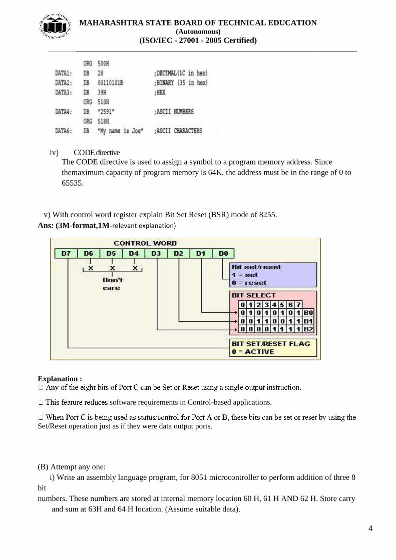
v) With control word register explain Bit Set Reset (BSR) mode of 8255.
Ans: (3M-format,1M-relevant explanation)
Explanation :
software requirements in Control-based applications.
Set/Reset operation just as if they were data output ports.
(B) Attempt any one:
i) Write an assembly language program, for 8051 microcontroller to perform addition of three 8
bit
numbers. These numbers are stored at internal memory location 60 H, 61 H AND 62 H. Store carry
and sum at 63H and 64 H location. (Assume suitable data).

MAHARASHTRA STATE BOARD OF TECHNICAL EDUCATION (Autonomous)
(ISO/IEC - 27001 - 2005 Certified) _____________________________________________________________________________________________
5
Ans: (3M-program,1M-comments)
Assume that RAM locations 60H – 62H have the following values.All values are in hex.
60=(7D) 61=(EB) 62=(C5)
PROGRAM:
MOV R0,#60H ; load pointer
MOV R2,#03H ; load counter
CLR A ; A=0
MOV R7,A ; clear R7
Again: ADD A,@R0 ; add the byte to A by pointer R0
JNC Next ; if CY=0 don‘t accumulate carry
INC R7 ; increment R7 if CY=1
Next: INC R0 ; increment pointer
DJNZ R2,Again ; repeat till 3 numbers are over
MOV 63H,A ; move the sum in 63H
MOV 64H,R7 ;move the carry in 64H
ii) Sketch 8051 microcontroller interfacing diagram to interface 4LEDS and 4 switches.
Interface LEDS to port 0 upper nibble and switch to port 1.Write an ALP for 8051 to read status of
switches and operate LEDs as per switch status.
Ans: (2M-Any correct diagram, 2M- correct program)
Program:
ORG 0000H
MOV P1, #0F0H ; Make P0 as input
START: MOV A, P1 ; Read status of the key
CJNE A, #0F0H, CHECK1; Key pressed branch from Port 0

MAHARASHTRA STATE BOARD OF TECHNICAL EDUCATION (Autonomous)
(ISO/IEC - 27001 - 2005 Certified) _____________________________________________________________________________________________
6
SJMP START ; Branch to start
CHECK1: ACALL DELAY ; Call delay
MOV A, P1 ; Read data from port 0
CPL A ; Complement A
MOV P0, A ; Send data to LED
AJMP START ; Jump to start
DELAY: MOV R6,#20H ; Delay program
NEXT1: MOV R7, #0FFH;
NEXT2: DJNZ R7, NEXT2;
DJNZ R6, NEXT1;
RET
END
2. Attempt any four:
a) Which pins of 8051 microcontrollers are used for external memory interfacing with 8051?
State their functions.
Ans: (1M-each )
The following pins of 8051 are used for external memory interfacing:
i) PSEN/:PSEN stands for ―program store enable.‖ In an 8031-based system in which an
external ROM holds the program code, this pin is connected to the OE pin of the ROM.
In other words, to access external ROM containing program code, the 8031/51 uses the
PSEN signal. When the EA pin is connected to GND, the 8031/51 fetches opcode from
external ROM by using PSEN. In systems based on the 8751/89C51/ DS5000 where EA
is connected to VCC, these chips do not activate the PSEN pin. This indicates that the
on- chip ROM contains program code.
ii) ALE: ALE stands for address latch enable. It is an output pin and is active high for
latching the low byte of address during accesses to external memory. The ALE pin is
used for demultiplexing the address and data by connecting to the G pin of the 74LS373
chip.
iii) EA/: EA stands for External access pin and it is active low. When it is held high,
executes instruction from the internal program memory till address OFFFH, beyond this
address the instructions are fetched from external program memory. If this pin is low ,
all the instructions are fetched from the external memory. During normal operation , this
pin should not be floated.(Should be connected to ground).
iv) RD(P3.7) and WR(P3.6): External data memory read and external data memory wite.
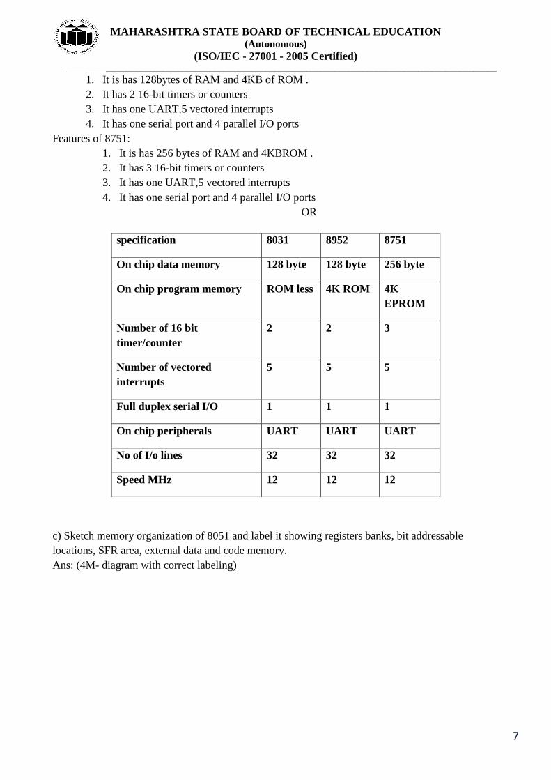
b) State two features of 8031, 8952 and 8751 microcontrollers.
Ans: (4M- any correct features)
Features of 8031:
1. It is has 128bytes of RAM but it is ROM less.
2. It has 2 16-bit timers or counters
3. It has one UART,5 vectored interrupts
4. It has one serial port and 4 parallel I/O ports.
Features of 8952:
MAHARASHTRA STATE BOARD OF TECHNICAL EDUCATION (Autonomous)
(ISO/IEC - 27001 - 2005 Certified) _____________________________________________________________________________________________
7
1. It is has 128bytes of RAM and 4KB of ROM .
2. It has 2 16-bit timers or counters
3. It has one UART,5 vectored interrupts
4. It has one serial port and 4 parallel I/O ports
Features of 8751:
1. It is has 256 bytes of RAM and 4KBROM .
2. It has 3 16-bit timers or counters
3. It has one UART,5 vectored interrupts
4. It has one serial port and 4 parallel I/O ports
OR
c) Sketch memory organization of 8051 and label it showing registers banks, bit addressable
locations, SFR area, external data and code memory.
Ans: (4M- diagram with correct labeling)
specification 8031 8952 8751
On chip data memory 128 byte 128 byte 256 byte
On chip program memory ROM less 4K ROM 4K
EPROM
Number of 16 bit
timer/counter
2 2 3
Number of vectored
interrupts
5 5 5
Full duplex serial I/O 1 1 1
On chip peripherals UART UART UART
No of I/o lines 32 32 32
Speed MHz 12 12 12

MAHARASHTRA STATE BOARD OF TECHNICAL EDUCATION (Autonomous)
(ISO/IEC - 27001 - 2005 Certified) _____________________________________________________________________________________________
8
Internal memory organization
OR
d) State significance of each bit of PSW register of 8051 microcontroller.
Ans: (2M-format,2M-function)

MAHARASHTRA STATE BOARD OF TECHNICAL EDUCATION (Autonomous)
(ISO/IEC - 27001 - 2005 Certified) _____________________________________________________________________________________________
9
1. CY: the carry flag. This flag is set whenever there is a carry out from the D7 bit.
The flag bit is affected after an 8 bit addition or subtraction. It can also be set to 1 or 0 directly by an instruction such as ―SETB C and CLR C where SETB
C stands for - set bit carry and CLR C for - clear carry. 2. AC: the auxiliary carry flag
If there is a carry from D3 and D4 during an ADD or SUB operation, this bit is set; it is cleared. This flag is used by instructions that perform BCD (binary coded decimal) arithmetic.
3. F0: Available to the user for general purposes. 4. RS0, RS1: register bank selects bits
These two bits are used to select one of the four register banks n internal RAM in the table. By writing zeroes and ones to these bits, a group of registers R0- R7 can be used out of four registers banks in internal RAM.
5. OV: the overflow flag
This flag is set whenever the result of a signed number operation is too large, causing the high-order bit to overflow into the sign bit. In general, the carry flag is used to detect errors in unsigned arithmetic operations. The overflow flag is only used to detect errors in signed arithmetic operations.
6. P: Parity flag
The parity flag reflects the number of 1s in the A (accumulator) register only. If the A register

MAHARASHTRA STATE BOARD OF TECHNICAL EDUCATION (Autonomous)
(ISO/IEC - 27001 - 2005 Certified) _____________________________________________________________________________________________
10
contains an odd number of 1‘s, then P=1, P=0 if A has an even number of 1‘s.
e) Explain reset operation for 8051 with reset circuit and reset signal.
Ans: (2M-diagram,2M-explanation)
Function of RESET: 1. Pin 9 is the RESET pin. It is an input and is active high (normally low). Upon applying a high
pulse to this pin, the microcontroller will reset and terminate all activities. 2. This is often referred to as a power-on reset. Activating a power-on reset will cause all values in
the registers to be lost. It will set program counter to all 0s. 3. In order for the RESET input to be effective, it must have a minimum duration of two machine
cycles. In other words, the high pulse must be high for a minimum of two machine cycles before it is allowed to go low.
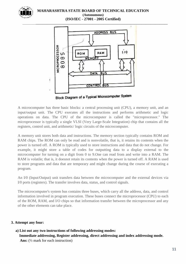
f) Sketch block diagram of microcomputer. Label each block and states function of each block.
Ans: (2M-diagram, 2M-function)
Any relevant and correct explanation should be given marks.
OR
MAHARASHTRA STATE BOARD OF TECHNICAL EDUCATION (Autonomous)
(ISO/IEC - 27001 - 2005 Certified) _____________________________________________________________________________________________
11
A microcomputer has three basic blocks: a central processing unit (CPU), a memory unit, and an
input/output unit. The CPU executes all the instructions and performs arithmetic and logic
operations on data. The CPU of the microcomputer is called the "microprocessor." The
microprocessor is typically a single VLSI (Very Large-Scale Integration) chip that contains all the
registers, control unit, and arithmetic/ logic circuits of the microcomputer.
A memory unit stores both data and instructions. The memory section typically contains ROM and
RAM chips. The ROM can only be read and is nonvolatile, that is, it retains its contents when the
power is turned off. A ROM is typically used to store instructions and data that do not change. For
example, it might store a table of codes for outputting data to a display external to the
microcomputer for turning on a digit from 0 to 9.One can read from and write into a RAM. The
RAM is volatile; that is, it doesnot retain its contents when the power is turned off. A RAM is used
to store programs and data that are temporary and might change during the course of executing a
program.
An I/0 (Input/Output) unit transfers data between the microcomputer and the external devices via
I/0 ports (registers). The transfer involves data, status, and control signals.
The microcomputer's system bus contains three buses, which carry all the address, data, and control
information involved in program execution. These buses connect the microprocessor (CPU) to each
of the ROM, RAM, and I/O chips so that information transfer between the microprocessor and any
of the other elements can take place.
3. Attempt any four:
a) List out any two instructions of following addressing modes:
Immediate addressing, Register addressing, direct addressing and index addressing mode.
Ans: (½ mark for each instruction)

MAHARASHTRA STATE BOARD OF TECHNICAL EDUCATION (Autonomous)
(ISO/IEC - 27001 - 2005 Certified) _____________________________________________________________________________________________
12
Immediate addressing mode:
MOV A, #25H ; Load 25H into A
MOV R2,#05H ;Load 05H into R2
Register Addressing mode:
ADD A, R5 ; Add the contents of register R5 to contents of A (accumulator)
MOV R2, A ; Move contents of Accumulator to R2
Direct Addressing mode:
MOV R0, 40H ; Save contents of RAM location 40H in R0.
ADD A,50H ; Add contents of memory location 50H &accumulator &store result in
Accumulator.
Indexed Addressing mode:
MOVC A, @A+DPTR
MOVC is a move instruction, which moves data from the external code memory space. The
address operand in this example is formed by adding the content of the DPTR register to the
accumulator value. Here the DPTR value is referred to as the base address and the accumulator
value us referred to as the index address.
MOVC A,@A+PC
b) State difference between SJMP, LJMP and AJMP instruction of 8051 microcontrollers.
Ans: (4 Marks—any two differences)
SJMP LJMP AJMP
SJMP jumps unconditionally
to the address
specified reladdr
LJMP jumps unconditionally
to the specified code addr.
AJMP unconditionally jumps
to the indicated code
address.
It is a two-byte instruction. It is a three-byte instruction. It is a two-byte instruction.
Reladdr must be within -128
or +127 bytes of the
instruction that follows the
SJMP instruction.
The code address in LJMP
can be any address anywhere
in the 64 K code space
Since only 11 bits of the
Program Counter are affected
by AJMP, jumps may only be
made to code located within
the same 2k block as the first
byte that follows AJMP
MAHARASHTRA STATE BOARD OF TECHNICAL EDUCATION (Autonomous)
(ISO/IEC - 27001 - 2005 Certified) _____________________________________________________________________________________________
13
c) Write single instruction to perform following operation:
i) Logical instruction to make accumulator content FFH.
ii) To set carry flag bit.
iii) To change content of accumulator from 85 H to 58 H.
iv) Jump of bit R 0.5 is ‘0’.
Ans: (1M-each correct instrution)
i) Logical instruction to make accumulator content FFH: ORL A, FF H
ii) To set carry flag bit: SETB C
iii) To change content of accumulator from 85 H to 58 H: SWAP A
iv) Jump of bit R 0.5 is ‗0‘: JNB P0.5,radd
Note: Since R0.5 is incorrect, marks should be given for any correct instruction.
d) Write assembly language program for 8051 to perform addition, if bit P 2.5 is set and
subtraction if that bit is clear i.e. ‘0’. Data 1 is at accumulator and data 2 is at 40 H address.
Ans: (4 Marks—any correct program)
MOV R0, #40H ;Load the address of data 2
JB P2.5, start ;If P2.5 is set, go to specified address, else go to next address
SUBB A, R0 ;Subtract data 1 (is at accumulator) and data 2 (is at 40 H address)
start: ADD, A, R0 ;If bit is set, add data 1 and data 2.
Sjmp $
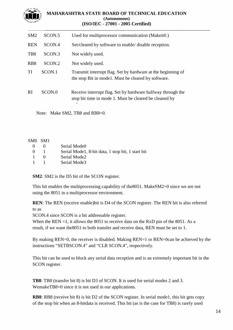
e) State function of each bit of SCON register. Draw format of SCON register.
Ans:(SCON register format - -2 Marks, Explanation of each bit --2 Marks)
SM0 SM1 SM2 REN TB8 RB8 TI RI
SM0 SCON.7 Serial port mode specifier
SM1 SCON.6 Serial port mode specifier.
MAHARASHTRA STATE BOARD OF TECHNICAL EDUCATION (Autonomous)
(ISO/IEC - 27001 - 2005 Certified) _____________________________________________________________________________________________
14
SM2 SCON.5 Used for multiprocessor communication (Makeit0.)
REN SCON.4 Set/cleared by software to enable/ disable reception.
TB8 SCON.3 Not widely used.
RB8 SCON.2 Not widely used.
TI SCON.1 Transmit interrupt flag. Set by hardware at the beginning of
the stop Bit in mode1. Must be cleared by software.
RI
SCON.0
Receive interrupt flag. Set by hardware halfway through the
stop bit time in mode 1. Must be cleared be cleaned by
software.
Note: Make SM2, TB8 and RB8=0.
SM0 SM1
0 0 Serial Mode0
0 1 Serial Mode1, 8-bit data, 1 stop bit, 1 start bit
1 0 Serial Mode2
1 1 Serial Mode3
SM2: SM2 is the D5 bit of the SCON register.
This bit enables the multiprocessing capability of the8051. MakeSM2=0 since we are not
using the 8051 in a multiprocessor environment.
REN: The REN (receive enable)bit is D4 of the SCON register. The REN bit is also referred
to as
SCON.4 since SCON is a bit addressable register.
When the REN =1, it allows the 8051 to receive data on the RxD pin of the 8051. As a
result, if we want the8051 to both transfer and receive data, REN must be set to 1.
By making REN=0, the receiver is disabled. Making REN=1 or REN=0can be achieved by the
instructions ―SETBSCON.4‖ and ―CLR SCON.4‖, respectively.
This bit can be used to block any serial data reception and is an extremely important bit in the
SCON register.
TB8: TB8 (transfer bit 8) is bit D3 of SCON. It is used for serial modes 2 and 3.
WemakeTB8=0 since it is not used in our applications.
RB8: RB8 (receive bit 8) is bit D2 of the SCON register. In serial mode1, this bit gets copy
of the stop bit when an 8-bitdata is received. This bit (as is the case for TB8) is rarely used

MAHARASHTRA STATE BOARD OF TECHNICAL EDUCATION (Autonomous)
(ISO/IEC - 27001 - 2005 Certified) _____________________________________________________________________________________________
15
any more. In all our applications wewillmakeRB8=0.Like TB8, the RB8 bit is also used in
serial modes 2and 3.
TI: TI (transmit interrupt)is bit D1 of the SCON register. This is an extremely important
flag bit in the SCON register.
When the 8051 finishes the transfer of the 8-bit character, it raises the T1flagto indicate
that it is ready to transfer another byte. The TI bit is raised at the beginning of the stop bit.
RI: RI(receive interrupt)is theD0 bit of the SCON register. This is another extremely
important flag in the SCON register.
When the 8051 receives data serially via RxD, it gets rid of the start and stop bits and
places the byte in the SBUF register.
Then it raises the RI flag bit to indicate that a byte has been received and picked up before it
is lost. RI is raised halfway through the stop bit.
4. (A) Attempt any three:
i) State role of assembler, editor, linker and loader in software development.
Ans: (1 Mark each tool)
Assembler: An assembler is programs that translate assembly language program to the correct binary code for each instruction i. e .machine code and generate the file called as Object file with extension . obj and list file with extension .lst extension. Some examples ofassemblerareASEM-51,Keil‟sA51,AX51 andC51, IntelPL /M-51etc.
Editor:
An editor is a program which helps you to construct your assembly language program in right format
so that the assembler will translate it correctly to machine language. So,you can type your program
using editor. This f orm of our program is called as source program and extension of program must
be asm or.src depending on which assembler is used.
The DOS based editor such as EDIT , WordStar, and Norton Editor etc .can be used to type your program.
Linker/Loader: A linker is a program, which combines ,if requested, more than one separately assembled object files into one ex ecutable p rogram , su ch as two o r more p rograms and a l s o gen e r a t e . abs file and initializes it with special instructions to facilitate its subsequent loading the execution.
Some examples of linker areASEM-51BL51,Keil u Vision Debugger, LX51 Enhanced Linker etc.
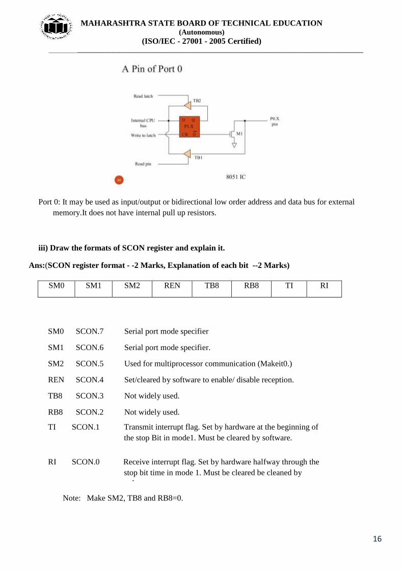
ii) Draw circuit diagram of Port 0 and state its alternate functions.
Ans:( 2 Marks—diagram,2 marks—functions)
MAHARASHTRA STATE BOARD OF TECHNICAL EDUCATION (Autonomous)
(ISO/IEC - 27001 - 2005 Certified) _____________________________________________________________________________________________
16
Port 0: It may be used as input/output or bidirectional low order address and data bus for external
memory.It does not have internal pull up resistors.
iii) Draw the formats of SCON register and explain it.
Ans:(SCON register format - -2 Marks, Explanation of each bit --2 Marks)
SM0 SM1 SM2 REN TB8 RB8 TI RI
SM0 SCON.7 Serial port mode specifier
SM1 SCON.6 Serial port mode specifier.
SM2 SCON.5 Used for multiprocessor communication (Makeit0.)
REN SCON.4 Set/cleared by software to enable/ disable reception.
TB8 SCON.3 Not widely used.
RB8 SCON.2 Not widely used.
TI SCON.1 Transmit interrupt flag. Set by hardware at the beginning of
the stop Bit in mode1. Must be cleared by software.
RI
SCON.0
Receive interrupt flag. Set by hardware halfway through the
stop bit time in mode 1. Must be cleared be cleaned by
software.
Note: Make SM2, TB8 and RB8=0.

MAHARASHTRA STATE BOARD OF TECHNICAL EDUCATION (Autonomous)
(ISO/IEC - 27001 - 2005 Certified) _____________________________________________________________________________________________
17
SM0 SM1
0 0 Serial Mode0
0 1 Serial Mode1, 8-bit data, 1 stop bit, 1 start bit
1 0 Serial Mode2
1 1 Serial Mode3
SM2: SM2 is the D5 bit of the SCON register.
This bit enables the multiprocessing capability of the8051. MakeSM2=0 since we are not
using the 8051 in a multiprocessor environment.
REN: The REN (receive enable)bit is D4 of the SCON register. The REN bit is also referred
to as
SCON.4 since SCON is a bit addressable register.
When the REN =1, it allows the 8051 to receive data on the RxD pin of the 8051. As a
result, if we want the8051 to both transfer and receive data, REN must be set to 1.
By making REN=0, the receiver is disabled. Making REN=1 or REN=0can be achieved by the
instructions ―SETBSCON.4‖ and ―CLR SCON.4‖, respectively.
This bit can be used to block any serial data reception and is an extremely important bit in the
SCON register.
TB8: TB8 (transfer bit 8) is bit D3 of SCON. It is used for serial modes 2 and 3.
WemakeTB8=0 since it is not used in our applications.
RB8: RB8 (receive bit 8) is bit D2 of the SCON register. In serial mode1, this bit gets copy
of the stop bit when an 8-bitdata is received. This bit (as is the case for TB8) is rarely used
any more. In all our applications wewillmakeRB8=0.Like TB8, the RB8 bit is also used in
serial modes 2and 3.
TI: TI (transmit interrupt)is bit D1 of the SCON register. This is an extremely important
flag bit in the SCON register.
When the 8051 finishes the transfer of the 8-bit character, it raises the T1flagto indicate
that it is ready to transfer another byte. The TI bit is raised at the beginning of the stop bit.
RI: RI(receive interrupt)is theD0 bit of the SCON register. This is another extremely
important flag in the SCON register.
When the 8051 receives data serially via RxD, it gets rid of the start and stop bits and
places the byte in the SBUF register.
Then it raises the RI flag bit to indicate that a byte has been received and picked up before it
is lost. RI is raised halfway through the stop bit.

MAHARASHTRA STATE BOARD OF TECHNICAL EDUCATION (Autonomous)
(ISO/IEC - 27001 - 2005 Certified) _____________________________________________________________________________________________
18
iv) What is the role of SMOD bit in serial communication? Write instruction to set SMOD bit.
Ans: (3 Marks-explaination,1 Mark—instruction)
SMOD Double Baud rates bit. When set to 1 and Timer 1 is used to generate baud rate, and
the serial port is used in modes 1, 2, or 3.
When 8051 is powered up, D7 bit i.e. SMOD bit of PCON =0, we could set D7 of PCON
‗1‘ to double the baud rate in serial communication.
Instruction to set SMOD bit is MOV PCON , #80H.
(B) Attempt any one:
i) Write assembly language program to perform and AND, OR and XOR operation on two
data. Data 1 is at internal RAM location 40 H and Data 2 is at external memory location
2000 H. Store result at three successive locations in internal RAM i.e. 50 H, 51 H and 52
H respectively.
Ans: (6 Marks-Any correct program)
MOV DPTR,#2000H ;Load external ML in DPTR
MOV A,@DPTR ;Load contents of external memory into accumulator
MOV R0,#40H :Initialize memory pointer
ANL A,@ R0 :AND data 1 and data 2
MOV 50H,A ;store result in Mem location 50 H
MOV A,@DPTR ;Load contents of external memory into accumulator
ORL A, @R0 ;OR data 1 and data 2
MOV 51H,A ;store result in Mem location 51 H
MOV A,@DPTR ;Load contents of external memory into accumulator
XLA A, @R0 ;EX- OR data 1 and data 2
MOV 52H, A ;store result in Mem location 52 H
SJMP $

MAHARASHTRA STATE BOARD OF TECHNICAL EDUCATION (Autonomous)
(ISO/IEC - 27001 - 2005 Certified) _____________________________________________________________________________________________
19
ii) Sketch interfacing diagram showing interfacing of two, 4K into 8 RAM chips with 8051
microcontrollers. Draw memory map.
Ans: (3 Marks—correct interfacing diagram,3 Marks—memory map)
Memory map
A15 A14 A13 A12 A11 A10 A9 A8 A7 A6 A5 A4 A3 A2 A1 A0 ADDR
Start 0 0 0 0 0 0 0 0 0 0 0 0 0 0 0 0 0000H addr Of
RAM 1
End 0 0 0 0 1 1 1 1 1 1 1 1 1 1 1 1 0FFFH addr Of
RAM 1
Start 0 0 1 0 0 0 0 0 0 0 0 0 0 0 0 0 2000H addr Of
RAM 2
End 0 0 1 0 1 1 1 1 1 1 1 1 1 1 1 1 2FFFH
addr of
RAM 2
MAHARASHTRA STATE BOARD OF TECHNICAL EDUCATION (Autonomous)
(ISO/IEC - 27001 - 2005 Certified) _____________________________________________________________________________________________
20
Q 5)Attempt any four:
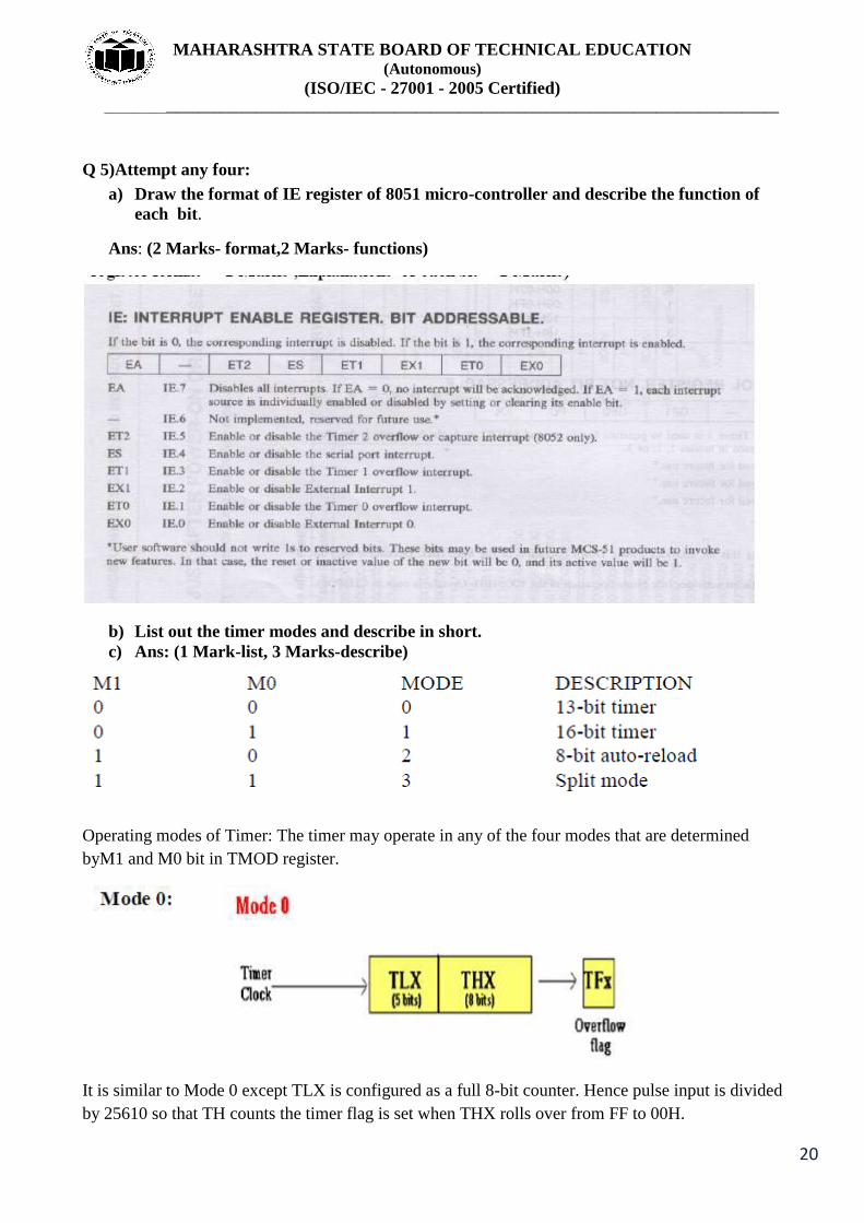
a) Draw the format of IE register of 8051 micro-controller and describe the function of
each bit.
Ans: (2 Marks- format,2 Marks- functions)
b) List out the timer modes and describe in short.
c) Ans: (1 Mark-list, 3 Marks-describe)
Operating modes of Timer: The timer may operate in any of the four modes that are determined
byM1 and M0 bit in TMOD register.
It is similar to Mode 0 except TLX is configured as a full 8-bit counter. Hence pulse input is divided
by 25610 so that TH counts the timer flag is set when THX rolls over from FF to 00H.

MAHARASHTRA STATE BOARD OF TECHNICAL EDUCATION (Autonomous)
(ISO/IEC - 27001 - 2005 Certified) _____________________________________________________________________________________________
21
It is similar to Mode 0 except TLX is configured as a full 8-bit counter. Hence pulse input is divided
by 25610 so that TH counts the timer flag is set when THX rolls over from FF to 00H.
In this mode only TLX is used as 8-bit counter. THX is used to hold the value which is loaded in
TLX initially. Every time TLX overflows from FFH to 00H the timer flag is set and the value from
THX is automatically reloaded in TLX register.
In this mode, timer 0 becomes two completed separate 8-bit timers. TL0 is controlled by gate
arrangement of timer 0 and sets timer 0 flag when it overflows. TH0 receives the timer clock under
the control of TR1 bit and sets TF1 flag when it overflows. Timer 1 may be used in mode 0, 1 and 2
with one important exception that no interrupt will be generated by the timer when the timer 0 is
using TF1 overflow flag.
c)What is interrupt? List out 8051 interrupts. Write instruction to disable anyone interrupt.
Ans: (1 Mark -definition, 2 Marks- list, 1 Mark—correct instruction)
Interrupt: It is a mechanism by which an I/O device (Hardware interrupt) or an instruction (software
interrupt) can suspend the normal execution of the processor and get itself serviced. Whenever an
interrupt occurs the controller completes the execution of the current instruction of an Interrupt
Service Routine(ISR). ISR is a piece of code that tells the controller what to do when an interrupt
MAHARASHTRA STATE BOARD OF TECHNICAL EDUCATION (Autonomous)
(ISO/IEC - 27001 - 2005 Certified) _____________________________________________________________________________________________
22
occurs. After the execution of ISR, controller returns back to the instruction it has jumped from
(before the interrupt was received). The interrupts can either be hardware or software interrupts
OR
The interrupt refers to a notification, communicated to the controller, by a hardware device or
software, on receipt of which the controller momentarily stops and responds to the interrupt.
Whenever an interrupt occurs the controller completes the execution of the current instruction of an
Interrupt Service Routine(ISR). ISR is a piece of code that tells the controller what to do when an
interrupt occurs. After the execution of ISR, controller returns back to the instruction it has jumped
from (before the interrupt was received). The interrupts can either be hardware or software
interrupts
There are Five interrupt sources of 8051 of which 2 are external and 3 are internal excluding the
reset interrupt.
Interrupt Flag Vector
System reset RST 0000H
External interrupt 0 IE0 0003H
Timer 0 TF0 000BH
External interrupt 1 IE1 0013H
Timer 1 TF1 001BH
Serial port RI or TI 0023H
Instruction: MOV IE, #8FH//disables the external interrupt 0 and enables all other interrupts
d)Write assembly language program to read data from port 3. Rotate that data by 4 times to
left and output it to port 1
ANS;(4 Marks –any correct program)
MOV A,P3 ; Read data from port 3
RLA ;Rotate the data four times to left
RLA
RLA
RLA
MOV PI,A ;Send to port 1
SJMP HERE
MAHARASHTRA STATE BOARD OF TECHNICAL EDUCATION (Autonomous)
(ISO/IEC - 27001 - 2005 Certified) _____________________________________________________________________________________________
23
d) Write assembly language program to transmit data 75H serially. At the end of
transmission make accumulator content as FFH. Ans: (4 Marks—any correct
program)
MOV TMOD, #20H ;TIMER 1,MODE 2
MOV TH1, #-3 ; 9600 baud rate
MOV SCON, #50H ; bit,1 stop bit,REN enabled
SETB TR1 ;Start timer 1
MOV A, #75H ; copy date 75h to accumulator
ACALL DELAY ; call delay
MOV A, #FFH ; move data FFh to accumulator
DELAY: MOV SBUF,A ;load SBUF
JNB TI, $ ;wait for last bit to transfer
CLR TI ;clear Transmit interrupt flag
RET
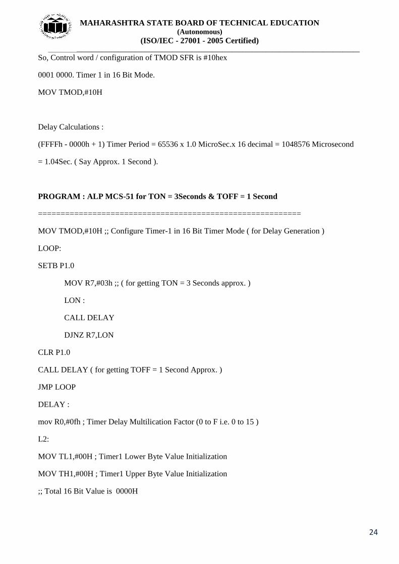
6. Attempt any four
a) Write assemble language program to generate pulse train. Assume suitable value for Toff
.Ton=3Toff. Assume Crystal Frequency as 12MHz.
(4m)
Ans:- ( Deciding count & Delay calculations: 2 M; Program :2 M)
Toff . Ton = 3Toff
Ton = 3Toff/Toff
Let us consider Ton = 3 sec, then Toff = 1 sec
Count for Ton = 3/1 = 3 and count for Toff = 1/1 = 1
Considering Freq= 12 MHZ .
Timer Clock = Freq /12 = 12MHZ/12 = 1MHZ .
i.e. Timer Period = 1 Microsec.
Ex. : We may use Timer 1 in 16 Bit Mode.
MAHARASHTRA STATE BOARD OF TECHNICAL EDUCATION (Autonomous)
(ISO/IEC - 27001 - 2005 Certified) _____________________________________________________________________________________________
24
So, Control word / configuration of TMOD SFR is #10hex
0001 0000. Timer 1 in 16 Bit Mode.
MOV TMOD,#10H
Delay Calculations :
(FFFFh - 0000h + 1) Timer Period = 65536 x 1.0 MicroSec.x 16 decimal = 1048576 Microsecond
= 1.04Sec. ( Say Approx. 1 Second ).
PROGRAM : ALP MCS-51 for TON = 3Seconds & TOFF = 1 Second
==========================================================
MOV TMOD,#10H ;; Configure Timer-1 in 16 Bit Timer Mode ( for Delay Generation )
LOOP:
SETB P1.0
MOV R7,#03h ;; ( for getting TON = 3 Seconds approx. )
LON :
CALL DELAY
DJNZ R7,LON
CLR P1.0
CALL DELAY ( for getting TOFF = 1 Second Approx. )
JMP LOOP
DELAY :
mov R0,#0fh ; Timer Delay Multilication Factor (0 to F i.e. 0 to 15 )
L2:
MOV TL1,#00H ; Timer1 Lower Byte Value Initialization
MOV TH1,#00H ; Timer1 Upper Byte Value Initialization
;; Total 16 Bit Value is 0000H

MAHARASHTRA STATE BOARD OF TECHNICAL EDUCATION (Autonomous)
(ISO/IEC - 27001 - 2005 Certified) _____________________________________________________________________________________________
25
SETB TR1 ;; Start Timer1
L3:
JNB TF1, L3 ;; Wait until generating Timer1 Overflow Flag
CLR TR1 ;; Stops Timer1
CLR TF1 ;; RESETs timer1 OVerflow Flag TF1
DJNZ R0,L2 ;; Timer1 x multiplying Factor as in R0 RAM Register
RET
END
b)State the meaning of interrupt priority. How it can be change? Explain with one example.
Ans:(4 Marks -correct answer)
All the 5 interrupts of 8051 has got different priorities. Interrupts are serviced according to it‘s
priority order. From the table above, you can see that INT0 has the highest priority of 1 and Timer 0
comes next with priority value 2. The order of priority works like this – consider a case where two
interrupts are raised at the same time – one from INT0 and another from Timer 1 interrupt. In such a
case, processor would serve the interrupt according to it‘s priority. In our case INT0 is of high
priority (priority order 1)and Timer 1 interrupt is of low priority (priority order 4). So processor will
execute ISR of INTO first and then later, after finishing ISR of INT0, processor will begin
executing ISR of Timer 1 interrupt
The priority of the interrupts can be modified by programming the contents of IP register.
c) Write 8051 instructions to operate port A, port B, port C of 8255 in simple I/O mode.
Ans:(4 Marks—all correct instructions)
; Port A,Port B,Port C as Input
MVI A,9B ; I/O control word
OUT CWR
; Port A,Port B,Port C as output
MVI 80H ;I/O control word

MAHARASHTRA STATE BOARD OF TECHNICAL EDUCATION (Autonomous)
(ISO/IEC - 27001 - 2005 Certified) _____________________________________________________________________________________________
26
OUT CWR
HLT
d) Explain auto-load timer mode. How it can be set?
Ans; (4 Marks-correct answer)
In this mode only TLX is used as 8-bit counter. THX is used to hold the value which is loaded in
TLX initially. Every time TLX overflows from FFH to 00H the timer flag is set and the value from
THX is automatically reloaded in TLX register.
It can be set by putting the value 02H in TMOD for timer0 mode2 or value 20H for timer1 mode 2.
MOV TMOD,#02H //timer 0 mode 2
MOV TMOD, #20H //timer 1 mode 2
e) List out any four selection factors for microcontroller and their importance in
applications.
Ans: (1 Mark—each factor)
The selection of microcontroller depends upon the type of application. The following factors
must be considered while selecting the microcontroller.
1. Word length: The word length of microcontroller is either 8, 16 or 32 bit. As the
word length increases, the cost, power dissipation and speed of the microcontroller
increases.
2. Power dissipation: It depends upon various factors like clock frequency, speed,
supply voltage, VLSI technology etc. For battery operated embedded systems, we must use
low power microcontrollers.
3. Clock frequency: The speed of an embedded system depends upon the clock
frequency. The clock frequency depends upon the application.
4. Instruction Set: On the basis of instructions microcontrollers are classified into two
Categories 1. CISC 2. RISC.
CISC system improves software flexibility. Hence it is used in general purpose systems.
RISC improves speed of the system for the particular applications.
MAHARASHTRA STATE BOARD OF TECHNICAL EDUCATION (Autonomous)
(ISO/IEC - 27001 - 2005 Certified) _____________________________________________________________________________________________
27
5. Internal resources: The internal resources are ROM, RAM, EEPROM, FLASH
ROM, UART, TIMER, watch dog timer, PWM, ADC, DAC, network interface, wireless
interface etc. It depends upon the application for which microcontroller is going to be used.
6. I/O capabilities: The number of I/O ports, size and characteristics of each I/O port,
speed of operation of the I/O port, serial port or parallel ports. These are the considerations
needed to ascertain.


