Low-Loss and High-Bandwidth
Multimode Polymer Waveguide Components
Using Refractive Index Engineering
Jian Chen, Nikos Bamiedakis, Peter Vasil'ev, Richard V. Penty, and Ian H. White
Electrical Engineering Division, University of Cambridge, UK
E-mail: [email protected]
Conference on Lasers and Electro-Optics (CLEO 2016)
June 6th, 2016

Outline
• Introduction to Optical Interconnects
• Board-level Optical Interconnects
• Multimode Polymer Waveguides
• Waveguide Components
o 90° Bends
o 90° Crossings
• Conclusions
1
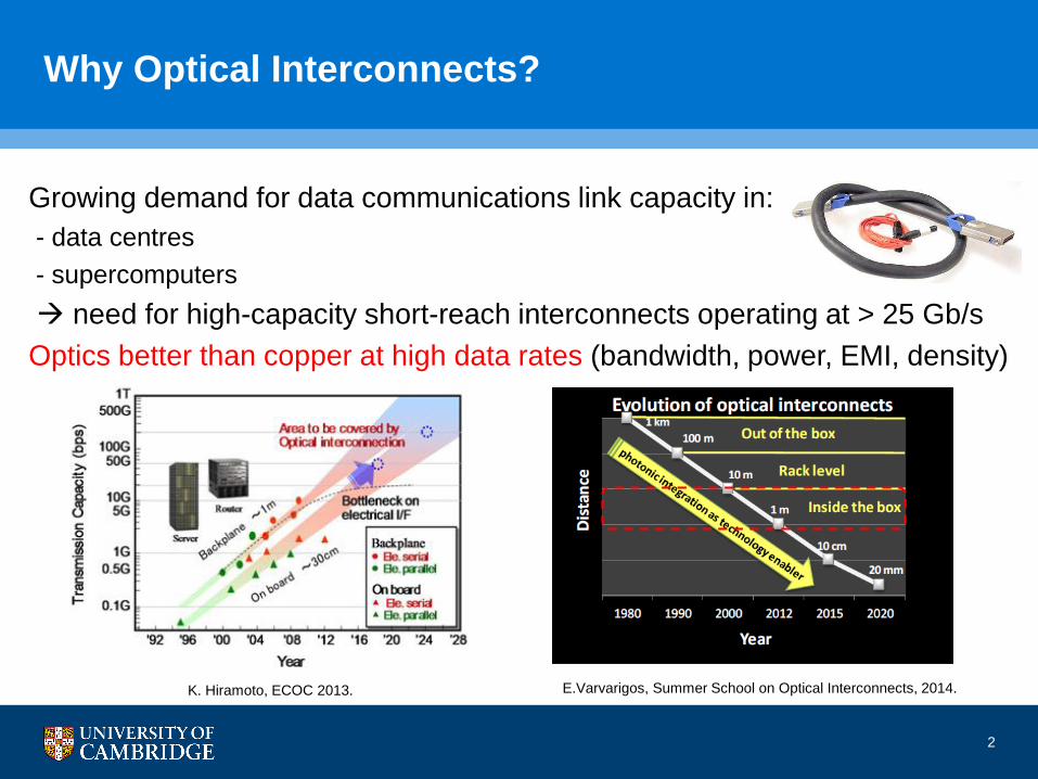
Why Optical Interconnects?
Growing demand for data communications link capacity in:
- data centres
- supercomputers
need for high-capacity short-reach interconnects operating at > 25 Gb/s
Optics better than copper at high data rates (bandwidth, power, EMI, density)
E.Varvarigos, Summer School on Optical Interconnects, 2014.K. Hiramoto, ECOC 2013.
2

Board-level Optical Interconnects
• Various approaches proposed:
free space interconnects
fibres embedded in substrates
waveguide-based technologies
M. Schneider, et al., ECTC 2009.
Jarczynski J. et al., Appl. Opt, 2006.R. Dangel, et al., JLT 2013.
Siloxane
waveguidesInterconnection
architectures
Board-level OE
integration PCB-integrated
optical units
Basic waveguide
components
Our work:
Polymer waveguides
3

Multimode Polymer Waveguides
- Siloxane Polymer Materials
• low intrinsic attenuation (0.03–0.05 dB/cm at 850 nm);
• good thermal and mechanical properties (up to 350 °C);
• low birefringence;
• fabricated on FR4, glass or silicon using standard techniques
• offer refractive index tunability
- Multimode Waveguide
• Cost-efficiency: relaxed alignment tolerances
assembly possible with pick-and-place machines
50 μm core
top cladding
bottom cladding
Substrate
suitable for integration on PCBs
offer high manufacturability
are cost effective
- typical cross section used: 50×50 μm2
- 1 dB alignment tolerances: > ±10 μm
4
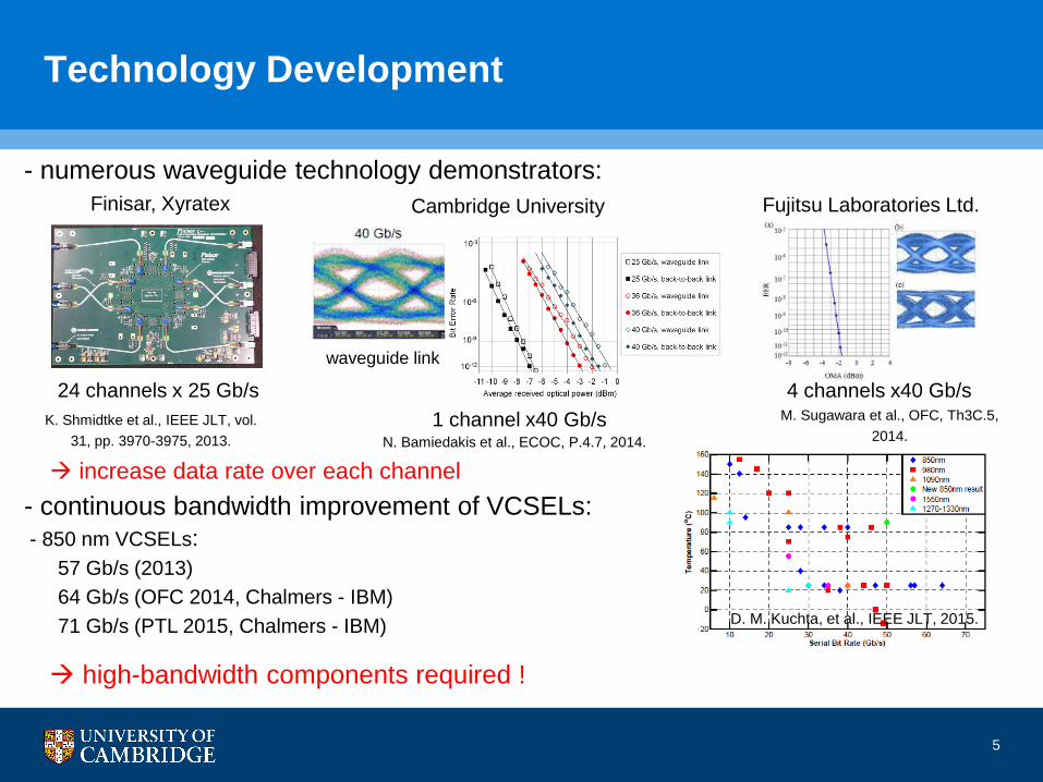
Technology Development
increase data rate over each channel
N. Bamiedakis et al., ECOC, P.4.7, 2014.
waveguide link
Finisar, Xyratex
24 channels x 25 Gb/s
K. Shmidtke et al., IEEE JLT, vol.
31, pp. 3970-3975, 2013.
4 channels x40 Gb/sM. Sugawara et al., OFC, Th3C.5,
2014.
Fujitsu Laboratories Ltd.
1 channel x40 Gb/s
Cambridge University
- numerous waveguide technology demonstrators:
- continuous bandwidth improvement of VCSELs:
- 850 nm VCSELs:
57 Gb/s (2013)
64 Gb/s (OFC 2014, Chalmers - IBM)
71 Gb/s (PTL 2015, Chalmers - IBM)
high-bandwidth components required !
D. M. Kuchta, et al., IEEE JLT, 2015.
5

Tx 1
Tx 2
Tx 3
Tx 4
Rx 1
Rx 2
Rx 3
Rx 4 90 bends
90 crossing
Multimode Waveguide Components
Tx 1
Tx 2
Tx 3
Tx 4
Rx 1
Rx 2
Rx 3
Rx 4 90 bends
90 crossing
Passive multimode waveguide components enable on-board routing flexibility and
advanced topologies:
90° crossing 90° bend S bend Y splitter
Elementary waveguide
components in complex
interconnection architectures
Components designed and fabricated:
- Waveguide crossings
- Bent waveguides: 90° bends, S bends
- Y-splitters/combiners
N. Bamiedakis et al., IEEE JQE, vol. 45, pp. 415-424, 2009.
J. Beals IV et al., Appl Phys A, vol. 95, pp. 983–988, 2009. 6

Interconnection Architectures
Waveguide crossings and bends elementary components in complex architectures
- meshed waveguide architecture: 1 Tb/s capacity optical backplane 100×10 Gb/s
links
- regenerative optical bus architecture 4 x 10 Gb/s links
10 × 10 cm2 FR4:
100 90° bends
~1800 90° crossings
5 × 9 cm2 FR4:
24 90° bends
36 90° crossings
8 S-bends
low-loss components required !
J. Beals, et al., Appl. Phys. A, vol. 95, pp. 983-988, 2009.
N. Bamiedakis et. al, IEEE JLT, vol. 32, pp. 1526-1537, 2014. 7

Waveguide Components
Radius: 5, 6, 8, 11, 15 and 20 mm
Number of crossings: 1, 5, 10, 20, 40 and 80
A B
A B
Length: ~137 mm
Length: ~137 mm
output
input
input
output
B
Length: ~137 mmA B
WG length: 16.25 cm
WG01 WG02 WG03
x(m)
y(
m)
-30 -20 -10 0 10 20 30-30
-20
-10
0
10
20
30
1.515
1.52
1.525
1.53
x(m)
y(
m)
-30 -20 -10 0 10 20 30-30
-20
-10
0
10
20
30
1.512
1.514
1.516
1.518
1.52
1.522
x(m)
y(
m)
-30 -20 -10 0 10 20 30-30
-20
-10
0
10
20
30
1.515
1.52
1.525
1.53
WG01 WG02 WG03
nmax 1.532 1.522 1.531
∆n 0.02 0.01 0.019
Height (μm) 37 53 48
Width (μm) 32 50 29
Radius: 5, 6, 8, 11, 15 and 20 mm
A BLength: ~137 mm
ALength: ~137 mm
BNumber of crossings: 1, 5, 10, 20, 40 and 80
B
Length: ~137 mmA B
Parameter WG01 WG02 WG03
max Δn 0.020 0.010 0.019
Size (µm2) 35 × 4055 × 5632 × 53
reference WGs 90° bends 90° crossings
- Components with different RI profiles and dimensions are fabricated and tested:
8
- Bends and crossings exhibit differing behaviours with respect to index step Δn:
bends benefit from larger Δn values (better light confinement)
crossings exhibit lower loss for smaller Δn values design trade-off

∆tin∆tout
Input pulse Output pulse1. Short pulse generation system
Femtosecond erbium-doped fibre laser at ~1574 nm
and a frequency-doubling crystal to generate pulses
at wavelength of ~787 nm
2. Matching autocorrelator to record output pulse
3. Convert autocorrelation traces back to pulse traces
curve fitting is needed to determine the shapes
of the original pulses, i.e. Gaussian, sech2 or Lorentzian.
4. Bandwidth calculation
waveguide frequency response and bandwidth estimated by comparing Fourier
transforms of input and output pulses
Bandwidth Estimation
0 0.5 1 1.5 2
x 1012
-20
-17
-14
-11
-8
-5
-2
0
Frequency (Hz)
Inte
nsity (
dB
)
Output pulse
Input pulse
3 dB
9

Reference Waveguides
- Insertion loss and bandwidth of reference waveguide measured under:
a restricted launch: 9/125 μm SMF input (loss) or 10× lens input (BW)
a 50/125 μm MMF input (likely encountered in a real-world system)
- restricted launch: similar insertion loss values (~1 dB) and large BLP (> 100 GHz×m)
- 50 μm MMF input: WG02 largest IL (~ 3 dB) but larger BLP (122 GHz×m) due to
smaller Δn value (0.01 vs 0.02)
B
Length: ~137 mmA B
WG length: 16.25 cm
10

Bends and Crossings
- Insertion loss the waveguide components measured under:
a restricted launch: 9/125 μm SMF input (loss)
a 50/125 μm MMF input (likely encountered in a real-world system)
- crossing loss (XL) and bending loss (BL) obtained by normalising with respect to the
insertion loss of the reference waveguides
0
1
2
3
4
5
6
7
8
9
0 20 40 60 80
Cro
ssin
g lo
ss (d
B)
Number of crossings
WG_A: 9 μm SMF
WG_Α: 50 μm MMF
WG_Β: 9 μm SMF
WG_Β: 50 μm MMF
WG_C: 9 μm SMF
WG_C: 50 μm MMF0
1
2
3
4
5
6
7
8
5 8 11 14 17 20B
en
din
g lo
ss (d
B)
Radius (mm)
WG01: 9 μm SMF
WG01: 50 μm MMF
WG02: 9 μm SMF
WG02: 50 μm MMF
WG03: 9 μm SMF
WG03: 50 μm MMF
- WG02 largest BL : R > 10 mm for 1 dB BL
but smallest XL: 0.02 dB/crossing for a 50 μm MMF input, < 0.01 dB/crossing for a
SMF input
- similar BL for WG01 and WG03: R > 6 mm for 1 dB BL, XL of WG01 worse
11
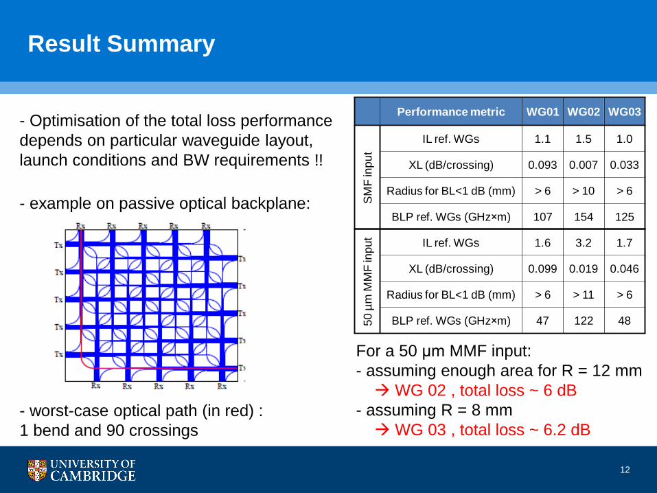
Result Summary
- Optimisation of the total loss performance
depends on particular waveguide layout,
launch conditions and BW requirements !!
- example on passive optical backplane:
- worst-case optical path (in red) :
1 bend and 90 crossings
Performance metric WG01 WG02 WG03
SM
F in
pu
t
IL ref. WGs 1.1 1.5 1.0
XL (dB/crossing) 0.093 0.007 0.033
Radius for BL<1 dB (mm) > 6 > 10 > 6
BLP ref. WGs (GHz×m) 107 154 125
50
µm
MM
F in
pu
t
IL ref. WGs 1.6 3.2 1.7
XL (dB/crossing) 0.099 0.019 0.046
Radius for BL<1 dB (mm) > 6 > 11 > 6
BLP ref. WGs (GHz×m) 47 122 48
For a 50 μm MMF input:
- assuming enough area for R = 12 mm
WG 02 , total loss ~ 6 dB
- assuming R = 8 mm
WG 03 , total loss ~ 6.2 dB
12

Conclusions
• Multimode polymer waveguides constitute an attractive technology for
use in board-level optical interconnects
• Waveguide bends and crossing are essential components in passive
interconnection architectures:
- optimisation of loss and BW performance is based on RI profile (index
step Δn and dimensions)
- depends on particular layout, BW requirements and launch conditions
• Low-loss and high-bandwidth (>47 GHz×m) multimode polymer
waveguide crossings (<0.02 dB/crossing) and bends (<1dB) are
demonstrated using refractive index engineering.
Acknowledgements:
13

References
[1]. N. Bamiedakis, J. Chen, R. V. Penty, and I. H. White, “High-Bandwidth and Low-Loss Multimode Polymer Waveguides
and Waveguide Components for High-Speed Board-Level Optical Interconnects,” in Photonics West conference, Proceeding
of SPIE, vol. 9753, pp. 975304–1–9 (2016).
[2]. N. Bamiedakis, A. Hashim, J. Beals IV, R. V. Penty, and I. H. White, "Low-Cost PCB-Integrated 10-Gb/s Optical
Transceiver Built With a Novel Integration Method," in IEEE Transactions on Components, Packaging and Manufacturing
Technology, Vol. 3, pp. 592-600 (2013).
[3]. J. Chen, N. Bamiedakis, P. Vasil’ev, T. Edwards, C. Brown, R. Penty, and I. White, “High-Bandwidth and Large Coupling
Tolerance Graded-Index Multimode Polymer Waveguides for On-board High-Speed Optical Interconnects,” in Journal of
Lightwave Technology, vol. 34, no. 12, pp. 2934–2940, (2015).
[4]. J. Beals, N. Bamiedakis, A. Wonfor, R. V. Penty, I. H. White, J. V. DeGrootJr., K. Hueston, T. V. Clapp, M. Glick, "A
terabit capacity passive polymer optical backplane based on a novel meshed waveguide architecture," in Applied Physics A:
Materials Science & Processing, Vol. 95, pp. 983-988 (2009).
[5]. N. Bamiedakis et al., "A 40 Gb/s Optical Bus for Optical Backplane Interconnections," in J. of Lightw. Techn., Vol. 32,
pp.1526-1537 (2014).
[6]. J. Chen, N. Bamiedakis, P. Vasil’ev, T. J. Edwards, C. T. A. Brown, R. V. Penty, and I. H. White, “Graded-Index Polymer
Multimode Waveguides for 100 Gb/s Board-Level Data Transmission,” in European Conference on Optical Communication,
no. 0613 (2015).
[7] J. Chen, N. Bamiedakis, T.J. Edwards, C. Brown, R.V. Penty, and I.H. White, “Dispersion Studies on Multimode Polymer
Spiral Waveguides for Board-Level Optical Interconnects,” in Proceedings of IEEE Optical Interconnects Conference, MD2,
San Diego (2015).
14

Thank you !
15


