
L. Rattia,c, E. Pozzatia,c, C. Andreolia,c, M. Manghisonib,c, V. Reb,c, V. Spezialia,c, G. Traversib,c
aUniversità degli Studi di Pavia
bUniversità degli Studi di Bergamo
cINFN Pavia
International Linear Collider WorkshopInternational Linear Collider Workshop
Valencia, 6-10 November 2006Valencia, 6-10 November 2006
CMOS Monolithic Sensors with Sparsified Readout and Time Stamping Capabilities
for Vertexing Applications at the ILC

2ILC Workshop 2006 – Valencia, 6-10 November 2006
MAPS for vertexing applications
Tracking and vertexing systems in future high luminosity colliders (ILC, SLHC, Super B-Factory) will be operated at high rate with low material budget to optimize position and momentum resolution
An ambitious goal is to design MAPS with similar readout functionalities as in hybrid pixels (sparsification, time stamping, e.g. FPIX)
A readout architecture with data sparsification would be a new feature which could give some advantages with respect to existing MAPS implementations
decouple modularity from readout speed
reduce digital power dissipation
flexibility in dealing with possible luminosity and background changes during the experiment lifespan
Modern VLSI CMOS processes (130 nm and below) could be exploited to increase the functionality in the elementary cell
Monolithic active pixel sensors (MAPS) may provide the required low mass and high granularity

3ILC Workshop 2006 – Valencia, 6-10 November 2006
In triple-well CMOS processes a deep N-well is used to isolate N-channel MOSFETs from substrate noise
Deep N-well structure
NMOS PMOS
P-substrate
Buried N-type layer
P-well
Standard N-well
P-epitaxial layer Such features were exploited in the development of deep N-well (DNW) MAPS devices
A DNW is used to collect the charge released in the epitaxial layer
A readout channel for capacitive detectors is used for Q-V conversion gain decoupled from electrode capacitance
NMOS devices of the analog section are built in the deep N-well
Using a large detector area, PMOS devices may be included in the front-end design charge collection inefficiency depending on the ratio of the DNW area to the area of all the N-wells (deep and standard)
Deep N-well MAPS concept

4ILC Workshop 2006 – Valencia, 6-10 November 2006
PMOSPMOSNMOS P-well
High sensitivity charge preamplifier with continuous reset
RC-CR shaper with programmable peaking time (0.5, 1 and 2 μs)
A threshold discriminator is used to drive a NOR latch featuring an external reset
A couple of test structures were fabricated in a 130 nm, triple well, epitaxial layer CMOS technology by STM
Preamplifier Shaper Discriminator Latch
Gm
A(s)
b0
b0
b1
b1
+
CF
C1
C2
Vt
RST
VF
~43 m
~4
3
mThe first prototypes proved the capability of the sensor to collect charge from the epitaxial layer
(G. Rizzo et al., “A novel monolithic active pixel detector in 0.13 μm triple well CMOS technology with pixel level analog processing”, NIMA vol. 565, pp. 195-201, 2006)
Pixel level processor (Apsel family)
5ILC Workshop 2006 – Valencia, 6-10 November 2006
0
10
20
30
40
50
60
0 200 400 600 800
EN
C [
e- rm
s]
Capacitance shunting the preamplifier input, CT [fF]
tP=1 s
measurement
simulation
in
out
I
CF
iF
eIN
eCSEE1
E2
VF
Series noise from current
source
Series noise from input
device
Parallel noise from the feedback
network
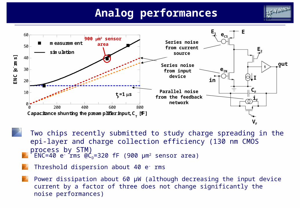
ENC=40 e- rms @CD=320 fF (900 μm2 sensor area)
Two chips recently submitted to study charge spreading in the epi-layer and charge collection efficiency (130 nm CMOS process by STM)
Threshold dispersion about 40 e- rms
Power dissipation about 60 μW (although decreasing the input device current by a factor of three does not change significantly the noise performances)
900 μm2 sensor area
Analog performances

6ILC Workshop 2006 – Valencia, 6-10 November 2006
ILC is expected to feature a beam structure with 2820 crossings per train (1 ms), with a duty-cycle of 0.5%
Chance of a single cell being hit twice in a bunch train is ≤ 1% for 20 μm x 20 μm or smaller pixels pipeline with a depth of one is sufficient to record ≥ 99% of events with no ambiguity data can be readout all together during the intertrain interval
Maximum hit occupancy is assumed to be 0.03 particles/crossing/mm2
3 hits/particle yield a hit rate of about 250 hits/train/mm2
Although the occupancy is quite small, a time stamp may prove useful to complement information from other detectors and reconstruct hit patterns
Sparsification reduces the amount of data sent off the chip and digital power dissipation
A DNW MAPS sensor for ILC is being designed based on a token passing readout scheme suggested by R. Yarema (R. Yarema, “Fermilab Initiatives in 3D Integrated Circuits and SOI Design for HEP”, ILC VTX Workshop at Ringberg, May 2006)
DNW MAPS for vertexing at the ILC

7ILC Workshop 2006 – Valencia, 6-10 November 2006
Preamplifier Discriminator
22T
14T
iF
CF Vt
Preamplifier response to an 800 e- pulse
Smaller area than in the Apsel prototypes smaller detector capacitance
ENC=25 e- rms@CD=100 fF
Power consumption: about 5 μW
Threshold dispersion: about 30 e- rms
Features power-down capabilities for power saving
-0.02
0
0.02
0.04
0.06
0.08
0.1
0.12
0 5 10 15 20 25 30
iF=3 nA
iF=5 nA
iF=10 nA
iF=15 nA
Pre
amp
lifie
r o
utp
ut
[V
]
t [s]
Cell analog front-end

8ILC Workshop 2006 – Valencia, 6-10 November 2006
199 ms
60 s
Switch-on transient
Preamplifier pulse response
1.2
0.0
0.0
0.2
0.4
0.6
V
ONOFF
The analog section in the elementary cell can be switched off during the intertrain interval in order to save power (analog power is supposed to be predominant over digital)
Based on circuit simulations, power cycling with at least 1% duty-cycle seems feasible
Considering the power available for the ILC vertex detector (20 W) and the vertex barrel area (about 170000 mm2), the available power/cell is ≥4.7 μW for a pitch of 20 μm or larger, compatible with the power dissipation features of the analog front-end
Preamplifier pulse response
Power cycling

9ILC Workshop 2006 – Valencia, 6-10 November 2006
OE
OEb
t1
t2
t3
t4
t5
t5in
t4in
t3in
t2in
t1in
CPb
CP
DQ
Qb
WE
hit
hitb
tokin
tokrsttokout
getb_enQ
QbLat_en
R
S
token passing
core
Get X bus
From the time stamp counter
To the time stamp buffer
Cell C
K
Get Y bus
Master Reset
time stamp
register
4T
10T 13T 20T
76T
From the discriminator
Cell C
Khit latch bus
control FF
Includes a 5 bit time stamp register and the data sparsification logic
During the bunch train period, the hit latch is set in each pixel that is hit
When the pixel is hit, the content of the time stamp register gets frozen
Cell digital section

10ILC Workshop 2006 – Valencia, 6-10 November 2006
X=1 X=16
Y=1
Y=2
Y=16
X=2Time Stamp
Buffer 1
Time Stamp
Buffer 2
Time Stamp
Buffer 16
Cell (1,1)
Cell (1,2)
Cell (1,16)
Cell (2,1)
Cell (2,2)
Cell (2,16)
Cell (16,1)
Cell (16,2)
Cell (16,16)
5 5 5
5554 4 4
4
4
4
4
45
MUX
Last token out
First token in
X
Y
T
Tkin Tkout
1 1 1
TkoutTkin
Tkin Tkout TkinTkout
TkoutTkin TkoutTkin
TkoutTkin TkoutTkin TkoutTkin
TS TS TS
1
1
1
Serial data output
gXb
gYb
TS TS TS
TS TS TS
Readout CK
gXb
gYb
gXb
gYb
gXb
gYb
gXb
gYb
gXb
gYb
gXb
gYb
gXb
gYb
gXb
gYb
Cell CK
gXb=get_X_bus
gYb=get_Y_bus
TS=Time_Stamp
Tkin=token_in
Tkout=Token_out
Digital readout scheme

11ILC Workshop 2006 – Valencia, 6-10 November 2006
Detection
0 1 2 3 4
30 31
Discriminator output
Hit
Token in
Token out
Output enable
Discriminator output
Hit
Token in
Token out
Output enable
X Y TSCELL (2,6)
X Y TSCELL (5,8)
Data output
Data output
Serial Data Output
Cell CK
Readout
CELL (2,6)
CELL (5,8)
CELL (2,6)
CELL (5,8)
(next hit cell)
first event
second event
Token arrives at cell (2,6)
Cell (2,6) data are read out
Cell (5,8) data are read out
Token arrives at cell (5,8)
Timing diagram

12ILC Workshop 2006 – Valencia, 6-10 November 2006
Time stamp register
•Preamplifier
•Discriminator
DNW sensor
Sparsification logic•Token passing core
•Hit-latch
•Bus control FF
•Nand gate
25
m
25 m
ILC DNW MAPS demonstrator
A 16x16 MAPS demonstrator chip is being designed in the 130 nm bulk CMOS technology by STM
Increase in the number of elements just requires larger X- and Y-registers and serializer
Further pitch reduction might be achieved by:
replacing the digital time stamp register with an analog one
using a further scaled process, namely a 90 nm CMOS technology by STM, supposed to have substrate features similar to those of the 130 nm process

13ILC Workshop 2006 – Valencia, 6-10 November 2006
A 90 nm CMOS process might provide some advantages in the design of DNW MAPS with respect to the 130 nm processabout a factor of two reduction in silicon area occupation
better power/channel thermal noise trade off
better 1/f noise performances
Normalized power spectral densities for NMOS devices belonging to the STM 130 and 90 nm processes
smaller dispersion in device parameters
Experimental characterization of test structures in 90 nm CMOS process will provide useful information as to the design of DNW MAPS
10-30
10-29
10-28
10-27
10-26
103 104 105 106 107 108
130 nm Technology90 nm Technology
SeW
LC
OX [
FV
2/H
z]
Frequency [Hz]
NMOS W/L=1000/0.35 @ Id=0.1 mA, Vds=0.6 V
be careful with gate currents
DNW MAPS in 90 nm CMOS

14ILC Workshop 2006 – Valencia, 6-10 November 2006
A DNW MAPS demonstrator aimed at vertexing applications at the ILC is being designed in a 130 nm bulk CMOS technology The chip is capable of
Further activities are under way to optimize the elementary cell size and geometry, includingsimplification of the pixel cell logic
MAPS development in a 90 nm CMOS technology
physical device simulations
Conclusions
The chip is capable of sparsified readout, time stamp generation and is compatible with power cycling operation
Simulations show good noise and threshold dispersion performances at a power dissipation close to the ILC vertex specifications


