
Integration of Photodefinable Polybenzoxazole as Intermetal Dielectric for
GaAs HBT Technology
Jiro Yota and Benny Do
GaAs Technology, Skyworks Solutions, Inc.
2427 W. Hillcrest Drive, Newbury Park, CA 91320, USA
Photodefinable polybenzoxazole (PBO) has been integrated as
intermetal dielectric in GaAs hetero-junction bipolar transistor
(HBT) technology. Process module optimization and integration
studies were performed and the results and process flow were
compared to those of dry-etch polyimide. The photodefinable
PBO is shown to allow the intermetal dielectric process flow to be
simplified and the number of processes and equipment to be
reduced. Results show that PBO has more planarity than
polyimide, when coated on GaAs HBT wafers, which typically
have significant topography. The photolithography coat, expose,
and develop processes were optimized to obtain the desired
dielectric thickness and the required via dimension and sidewall
profile, in addition the removal of the PBO from the die street.
The PBO thermal curing process was performed at 300oC, while
plasma ashing was performed to remove any PBO residue from the
bottom of the vias. These results show that the photodefinable
PBO film is compatible with, is suitable for, and can be integrated
as intermetal dielectric in GaAs HBT technology.
Introduction
Spin-on polymer dielectrics have been widely used for various applications in
semiconductor device fabrication, including in the processing of silicon and compound
semiconductors, such as GaAs. They are primarily used as intermetal dielectric,
redistribution layer, stress buffer and mechanical protection layer, and as encapsulant in
packaging [1-14]. Many of these spin-on dielectrics, which include both organic and
inorganic films, such as benzocyclobutene (BCB), spin-on glass (SOG), siloxane,
polyimide, and polybenzoxazole (PBO) have excellent electrical, chemical, and
mechanical characteristics [1,4,9,10,15-17]. In order to achieve these desired film
characteristics, most of these polymers typically have to be thermally cured at high
temperatures [5,10,12,17-19].
In general, the maximum temperature that can be employed in GaAs technology,
including GaAs hetero-junction bipolar transistor (HBT) technology, is 300oC or lower.
This is due to the degradation of the materials typically used in this technology at higher
temperatures, which include the metals used as contact materials to the GaAs devices and
epitaxial layers [5,7,20-24]. As a result, spin-on polymer dielectrics that have a curing
temperature that is higher than 300oC cannot be used. Furthermore, if a polymer
dielectric is considered for use as intermetal dielectric in GaAs technology, it has to be
compatible with the interconnection patterning and metallization methods that are used in
the technology. The metallization techniques typically used in GaAs technology may
include e-beam evaporation, sputtering, and electroplating, while the patterning and
removal methods may include wet or dry etch, and photoresist, dielectric, and metal
liftoff [22-28]. Depending on the processes used, different photoresist, dielectric, and
metal profiles may be obtained, which will result in different electrical and mechanical
characteristics of the film and the devices fabricated.
An important consideration in the evaluation of a polymer dielectric as intermetal
dielectric for GaAs technology is the planarity of the film when coated on top of the
underlying topography, including the metal interconnections, and the transistor and
epitaxial structures. In GaAs HBT technology, there are mesas, pedestals, and trenches,
which are created, when fabricating the emitter, base, and collector of the hetero-junction
bipolar transistors, which topography difference may be larger than 2 m. Furthermore,
the metal interconnection thickness in GaAs technology typically ranges from 1 m to 6
m, unlike the much thinner metal used in Si technology [7,22-24,27-29]. This thicker
metal will increase the topography on the GaAs HBT wafer. So, when measured from
the bottom of the lowest topography (bottom of the collector trench and the die street) to
the top of the highest topography (top of the Metal 1 on the emitter mesa of the HBT), the
topography height difference on a GaAs HBT wafer may well be 3 m or larger.
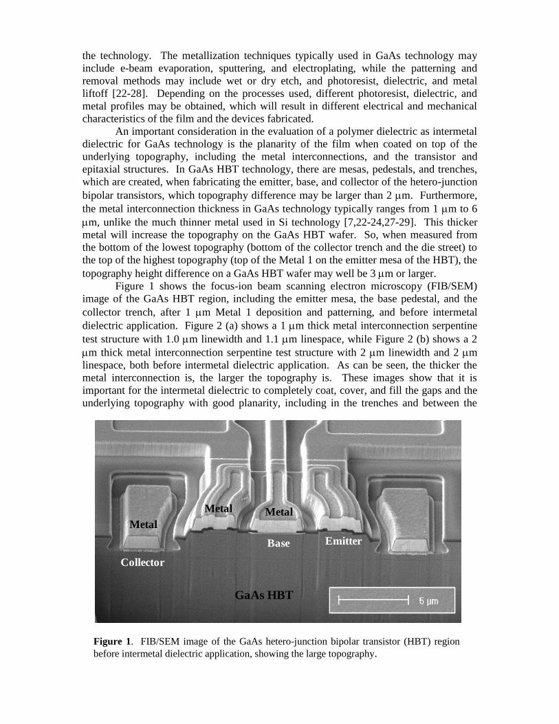
Figure 1 shows the focus-ion beam scanning electron microscopy (FIB/SEM)
image of the GaAs HBT region, including the emitter mesa, the base pedestal, and the
collector trench, after 1 m Metal 1 deposition and patterning, and before intermetal
dielectric application. Figure 2 (a) shows a 1 m thick metal interconnection serpentine
test structure with 1.0 m linewidth and 1.1 m linespace, while Figure 2 (b) shows a 2
m thick metal interconnection serpentine test structure with 2 m linewidth and 2 m
linespace, both before intermetal dielectric application. As can be seen, the thicker the
metal interconnection is, the larger the topography is. These images show that it is
important for the intermetal dielectric to completely coat, cover, and fill the gaps and the
underlying topography with good planarity, including in the trenches and between the
Figure 1. FIB/SEM image of the GaAs hetero-junction bipolar transistor (HBT) region
before intermetal dielectric application, showing the large topography.
Collector
EmitterBase
Metal
MetalMetal
GaAs HBT

metal spaces. A planar intermetal dielectric surface on various topographies will make
multilevel metallization less challenging and allow devices to be built on top of each
other [7,29]. This will in turn allow and make possible the simplification of circuit
designs, and the shrinking and reduction of the die size.
One of the most widely used spin-on
polymer dielectric for GaAs HBT technology
is polyimide. Polymide has good mechanical
and electrical characteristics, including low
dielectric constant (=2.8-3.3) [3-
5,8,15,25,27,31,32]. Typically, the type of
polyimide used is dry-etch polyimide and is
applied by spin-coating the film on the wafer
and then curing in a thermal convection oven.
The via and intermetal dielectric patterning is performed by via photoresist coat, followed
by via expose and develop processes. The polyimide is then dry-etched to open the vias
and remove the polyimide from the die street, followed by performing via photoresist
removal and cleaning, and then overlying metallization and patterning. However, this
method is lengthy, inefficient, and costly, and requires a number of different equipment.
Furthermore, the via profile of the dry-etch polyimide has severe slope (closer to vertical)
with sharp angle at the top edge of the via. When overlying metal is deposited by e-beam
evaporation on top of the via, in most cases, the metal will have poor step coverage and
conformality on the via sidewall, and will result in metal cracks. Figure 3 (a) and (b)
show a via with Metal 2 completely filling the via, and a via with partial Metal 2 inside,
respectively. In both cases, the overlying Metal 2 has sidewall cracks on the via sidewall,
due to the poor metal step coverage. These metal cracks will lead to high via resistance,
and will result in device performance degradation and reliability failures [27,33].
Figure 2. FIB/SEM images of the metal
interconnection serpentine structure with a
topography and metal thickness of (a) 1 m and
(b) 2 m on top of GaAs, before intermetal
dielectric application.
(a)
(b)
(a)
(b)
Metal 2
Metal 1
Via
Metal 2
Metal 1
Via
Polyimide
Polyimide
Figure 3. FIB/SEM images of (a) via
with overlying Metal 2 inside the via
and (b) via with partial Metal 2 inside
the via, and with dry-etch polyimide as
intermetal dielectric.
Many of the existing polyimide and other polymer dielectric materials have to be
cured at high temperature and therefore are not compatible with GaAs technology.
Additionally, some of these films are not chemically resistant against and are not
compatible with the materials and chemicals typically used in GaAs technology, such as
electroplating chemicals, N-methyl-2-pyrrolidone (NMP), hydrogen peroxide, and
acetone [2,5,7,10,22-28]. It is also known that polyimide and many other polymer
dielectric films typically have high moisture absorption characteristics [3-
5,7,10,12,16,17,25,29-32]. All these incompatibilities can lead to degradation, cracks,
and delamination of the polymer, and absorption of moisture and chemicals into the film,
resulting in device performance and yield loss, and reliability failures
[5,7,10,27,28,31,32].
Recently, polybenzoxazole has become the polymer of choice for many thin-film
semiconductor applications. Similar to polyimide, PBO has low dielectric constant
(=2.9-3.2) and has good mechanical characteristics [2-5,7,14,27,28]. Additionally, PBO
has the advantage of not having the polar carbonyl group (C=O) that polyimide has.
Figure 4 shows the structure difference of a PBO monomer, compared to a polyimide
monomer which has the carbonyl group. The absence of this carbonyl functional group
in PBO prevents the formation of hydrogen bond between the polymer and water, and
therefore resulting in less water absorption in PBO film, compared to in polyimide.
PBO Polyimide
O O
X1Y1[ ]
n
NN
O O
X1Y1[ ]
n
NN
O
OO
O
[ X2 Y2]n
N N
O
OO
O
[ X2 Y2]n
N N
OO
O
[ X2 Y2]n
N N
PBO material is also known for its excellent thermal stability and thermo-
oxidative resistance [2-5,14,18,32]. The material is also easily processed, and with
photoactive compounds or photosensitizers, acts as a photoresist or hardmask during
etching [1,5,9,16,27,34,35]. The use of photosensitive and photodefinable PBO as
intermetal dielectric will simplify the process flow, by reducing the number of process
steps, improving the cycle time, and reducing the number of equipment used, when
compared to dry-etch polyimide. In the PBO intermetal dielectric flow, the photoresist
coating and removal, and polymer dry-etch and clean processes that are typically used
when dry-etch polyimide is used as intermetal dielectric, can be eliminated. Furthermore,
the developer that is used with this photodefinable PBO is tetramethyl ammonium
hydroxide (TMAH) in water, an environmentally benign aqueous solution.
In this study, we have characterized, developed, optimized, and integrated
photosensitive and photodefinable PBO film as an intermetal dielectric in GaAs HBT
technology. We evaluated the PBO process flow, including all the individual process
modules that are required to process the material, and compared to the dry-etch polymide
process flow and its process steps. The optimization of each module was discussed in
Figure 4. Example of a monomer of polybenzoxazole (PBO) vs.
monomer of polyimide with its polar C=O bonds, with X1, Y1, X2, and
Y2 being aliphatic and/or aromatic parts of the monomers.
order to resolve any integration issues, including the planarity of the film, the temperature
requirements, the via requirements, and the compatibility of the photosensitive PBO
material to GaAs HBT technology as an intermetal dielectric.
Experimental
The polybenzoxazole (PBO) polymer dielectric used in this study is XP8851-
X1 from HD MicroSystems and was applied to the wafers by spin-coating method. The
film is a positive-tone, photosensitive, and photodefinable material, and comprises the
PBO precursor, which is a polyamide, the photoactive compounds and crosslinkers, in
addition to the solvents of 2-methoxy-1-methylethyl acetate and -butyrolactone. The
photopackage in this PBO material is sensitive to the typical broadband exposure
between 350 and 465 nm.
The wafers used in this investigation are 150 mm diameter GaAs <100> wafers,
which were either bare GaAs test wafers, or GaAs hetero-junction bipolar transistor
(HBT) device-patterned wafers. The GaAs devices, including the hetero-junction bipolar
transistors and other active and passive devices, and the metal interconnections were
fabricated using a GaAs HBT technology utilizing various metals and dielectrics
deposition and patterning process steps. The films were deposited or coated on
underlying patterned HBT and interconnection metal (Metal 1), which comprises
evaporated Ti/Au/Ti stack with a thickness of 1 or 2 m. The thickness of the PBO film
coated ranges from 2.4 to 4 m, measured as-coated on bare GaAs wafers.
Since the PBO is photosensistive and photodefinable, the via photolithography
and patterning was performed by exposing and developing the intermetal dielectric film.
The expose process step was performed using an i-line stepper, while the develop process
step was performed in an aqueous solution of tetramethyl ammonium hydroxide (TMAH),
after which the film is then thermally cured at 300ºC for 1 hour in an convection oven.
Ashing of the vias in an oxygen plasma environment is performed after the develop
process step to ensure the cleanliness inside the vias. After the via patterning, curing, and
ashing, the GaAs wafers were then metal-patterned and deposited with evaporated
overlying top metal (Metal 2) of Ti/Au/Ti stack with a thickness of 2 m. The metal
patterning was performed using metal liftoff process, which uses the chemical N-methyl-
2-pyrrolidone (NMP).
The results obtained from the photodefinable PBO intermetal dielectric process
were compared to those obtained from a typical dry-etch polyimide process. The
polyimide used was PI2610 from HD MicroSystems. The polyimide was spun with an
as-coated thickness of 2 m on GaAs wafers, and was then thermally cured at 300ºC for
1 hour, after which the via photoresist was applied on top of the polyimide. Via
patterning was performed by exposing and developing the photoresist, dry-etching the
polyimide in oxygen-based plasma chemistry to open the vias, removing the polyimide
from the street, cleaning and ashing the vias, and stripping and removing the photoresist.
Focus-ion beam scanning electron microscope (FIB/SEM) analysis was
performed using a FEI Nova 600i dual beam system to evaluate the planarity and gapfill
capability of spin-on PBO and polyimide intermetal dielectric films. Furthermore, the
profile of these films and the vias formed on top of both the hetero-junction bipolar
transistors and metal interconnections were studied and compared. Additionally, the step
coverage, conformality, and continuity of the overlying metal (Metal 2) into the vias and
on top of these dielectrics with various topographies were analyzed as well.

Results and Discussion
Thickness and Coating Process - In order to be able to use the spin-on PBO
polymer as intermetal dielectric in GaAs HBT technology, the PBO spin-speed thickness
curve was collected on bare test wafers and the results were evaluated and correlated to
the thickness on actual GaAs HBT device wafers with the topography. Figure 5 shows
the spin-speed curve of the PBO as-coated, after develop, and after develop and cure
processes, with the thicknesses plotted as a function of the spin-speed. As can be seen,
the as-coated thickness of the PBO was reduced in subsequent develop and cure process
steps. The spin speed curve shows that the PBO can be coated over a wide range of
thickness, ranging from as-coated thickness of 2.4 m to 4 m, which corresponds to
after develop and cure thickness
of 1.8 to 3.2 m, on bare GaAs
test wafers. This thickness range
makes this material to be very
suitable as intermetal dielectric
for GaAs technology, which has
significant topography, due to the
presence of the transistors and
the thick metal interconnections.
The desired PBO thickness can
be obtained by optimizing the
coat and the subsequent develop
and cure process steps, and can
be selected based on the
thickness requirement on top of
the underlying topography and on
the electrical, mechanical, and
reliability requirements of the
devices.
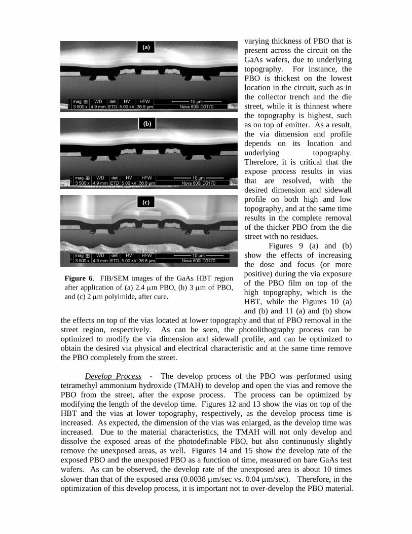
Figures 6 (a) and (b) show the after cure images of the hetero-junction bipolar
transistor region on GaAs wafer coated with 2.4 m and 3 m thick PBO film, while
Figure 6 (c) shows the after-cure image of a wafer coated with 2 m polyimide film.
Figures 7 (a)-(c) and Figures 8 (a)-(c) show the cured PBO with the same 2 different
thicknesses and the cured polyimide on top of a large metal plate on a base pedestal mesa
and on top of metal interconnection serpentines, respectively. As can be seen, the PBO
is significantly more planar, as compared to polyimide, when the same thickness of
dielectric material (of about 0.9 m) was targeted and achieved on top of the highest
topography (which is the metal on top of the emitter in the HBT) as shown in Figure 6.
Expose Process - The photolithography expose process of the PBO was
developed and optimized by performing typical focus-exposure matrix experiments in
order obtain a condition that resulted in vias that are resolved and open, with the desired
dimension and sidewall profile. The dimension and sidewall profile of the via is
important in GaAs technology, as in many cases, e-beam evaporation or sputtering
method is used for metallization. These methods requires that the via sidewall profile to
be more positive (or less vertical with less severe slope) with no sharp angles in the via in
order to obtain better metal step coverage and conformality, and avoids cracks in the
metal inside the via. The photolithography process is made more complex due to the
1.0
1.5
2.0
2.5
3.0
3.5
4.0
4.5
1000 1500 2000 2500 3000 3500 4000 4500
Th
ick
ness
(
m)
Spin Speed (rpm)
As-Coated
After Develop
After Develop/Cure
Figure 5. Spin-speed curve of PBO (a) as-coated, (b)
after develop, and (c) after develop and cure
processes.
varying thickness of PBO that is
present across the circuit on the
GaAs wafers, due to underlying
topography. For instance, the
PBO is thickest on the lowest
location in the circuit, such as in
the collector trench and the die
street, while it is thinnest where
the topography is highest, such
as on top of emitter. As a result,
the via dimension and profile
depends on its location and
underlying topography.
Therefore, it is critical that the
expose process results in vias
that are resolved, with the
desired dimension and sidewall
profile on both high and low
topography, and at the same time
results in the complete removal
of the thicker PBO from the die
street with no residues.
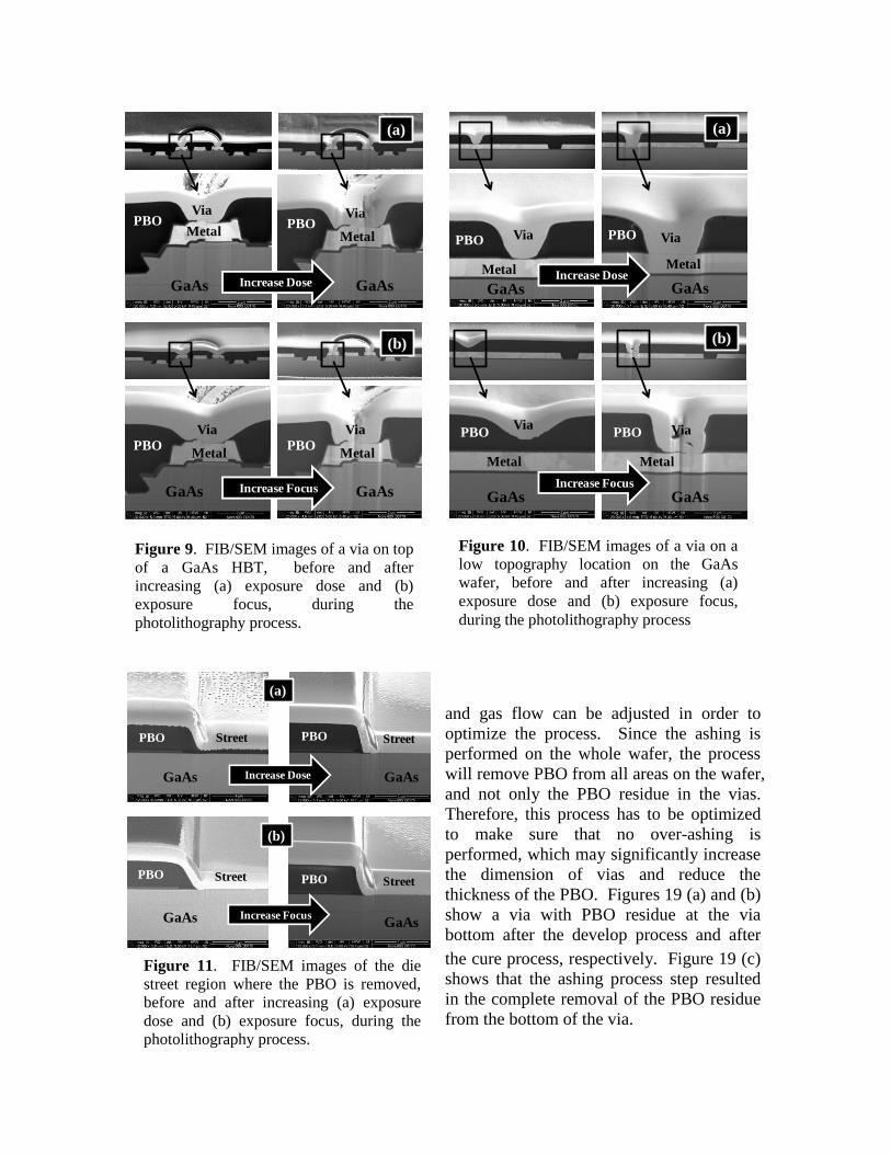
Figures 9 (a) and (b)
show the effects of increasing
the dose and focus (or more
positive) during the via exposure
of the PBO film on top of the
high topography, which is the
HBT, while the Figures 10 (a)
and (b) and 11 (a) and (b) show
the effects on top of the vias located at lower topography and that of PBO removal in the
street region, respectively. As can be seen, the photolithography process can be
optimized to modify the via dimension and sidewall profile, and can be optimized to
obtain the desired via physical and electrical characteristic and at the same time remove
the PBO completely from the street.
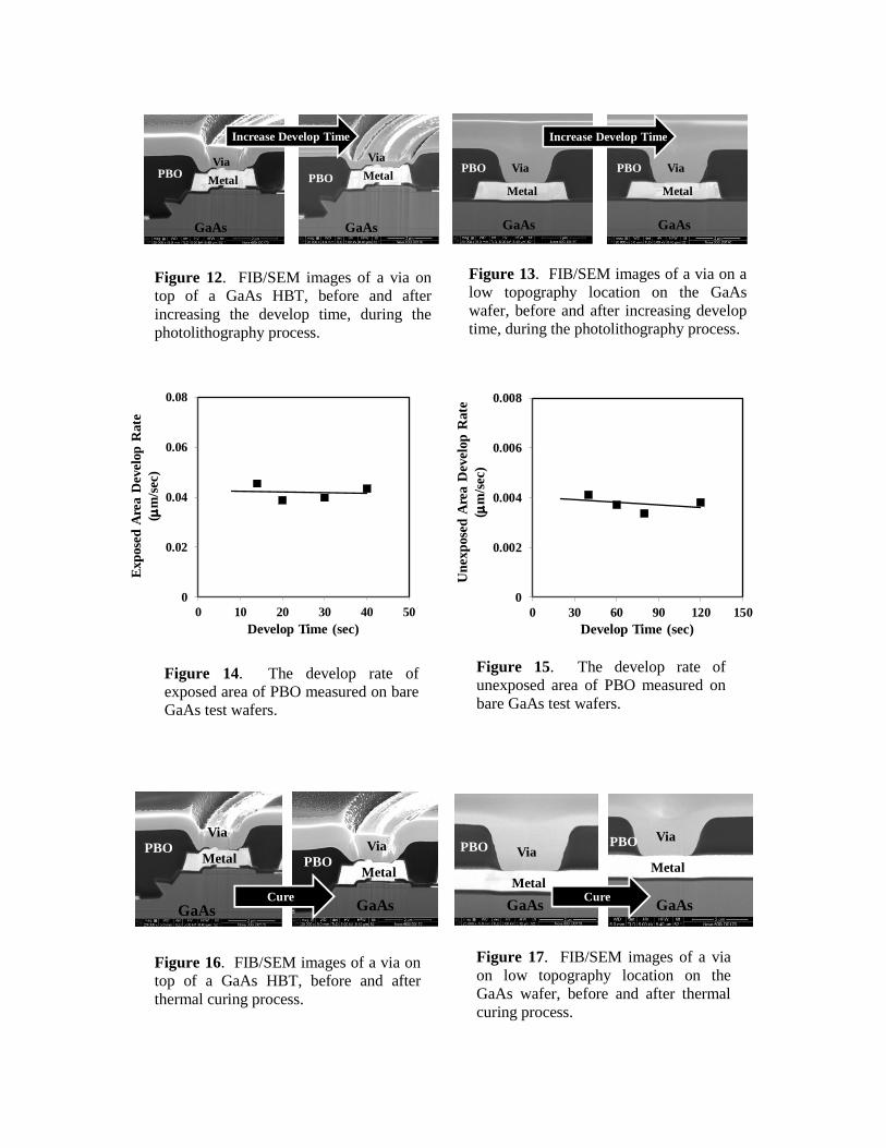
Develop Process - The develop process of the PBO was performed using
tetramethyl ammonium hydroxide (TMAH) to develop and open the vias and remove the
PBO from the street, after the expose process. The process can be optimized by
modifying the length of the develop time. Figures 12 and 13 show the vias on top of the
HBT and the vias at lower topography, respectively, as the develop process time is
increased. As expected, the dimension of the vias was enlarged, as the develop time was
increased. Due to the material characteristics, the TMAH will not only develop and
dissolve the exposed areas of the photodefinable PBO, but also continuously slightly
remove the unexposed areas, as well. Figures 14 and 15 show the develop rate of the
exposed PBO and the unexposed PBO as a function of time, measured on bare GaAs test
wafers. As can be observed, the develop rate of the unexposed area is about 10 times
slower than that of the exposed area (0.0038 m/sec vs. 0.04 m/sec). Therefore, in the
optimization of this develop process, it is important not to over-develop the PBO material.
Figure 6. FIB/SEM images of the GaAs HBT region
after application of (a) 2.4 m PBO, (b) 3 m of PBO,
and (c) 2 m polyimide, after cure.
(a)
(b)
(c)
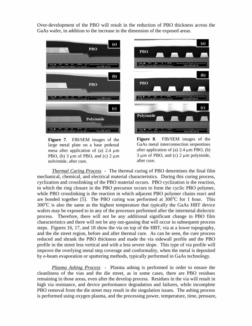
Over-development of the PBO will result in the reduction of PBO thickness across the
GaAs wafer, in addition to the increase in the dimension of the exposed areas.
Thermal Curing Process - The thermal curing of PBO determines the final film
mechanical, chemical, and electrical material characteristics. During this curing process,
cyclization and crosslinking of the PBO material occurs. PBO cyclization is the reaction,
in which the ring closure in the PBO precursor occurs to form the cyclic PBO polymer,
while PBO crosslinking is the reaction in which adjacent PBO polymer chains react and
are bonded together [5]. The PBO curing was performed at 300
oC for 1 hour. This
300oC is also the same as the highest temperature that typically the GaAs HBT device
wafers may be exposed to in any of the processes performed after the intermetal dielectric
process. Therefore, there will not be any additional significant change in PBO film
characteristics and there will not be any out-gassing that will occur in subsequent process
steps. Figures 16, 17, and 18 show the via on top of the HBT, via at a lower topography,
and the die street region, before and after thermal cure. As can be seen, the cure process
reduced and shrank the PBO thickness and made the via sidewall profile and the PBO
profile in the street less vertical and with a less severe slope. This type of via profile will
improve the overlying metal step coverage and conformality, when the metal is deposited
by e-beam evaporation or sputtering methods, typically performed in GaAs technology.
Plasma Ashing Process - Plasma ashing is performed in order to ensure the
cleanliness of the vias and the die street, as in some cases, there are PBO residues
remaining in those areas, even after the develop process. Residues in the via will result in
high via resistance, and device performance degradation and failures, while incomplete
PBO removal from the die street may result in die singulation issues. The ashing process
is performed using oxygen plasma, and the processing power, temperature, time, pressure,
(a)
PBO
PBO
Polyimide
(b)
(c)
(a)
PBO
PBO
Polyimide
(b)
(c)
Figure 7. FIB/SEM images of the
large metal plate on a base pedestal
mesa after application of (a) 2.4 m
PBO, (b) 3 m of PBO, and (c) 2 m
polyimide, after cure.
Figure 8. FIB/SEM images of the
GaAs metal interconnection serpentines
after application of (a) 2.4 m PBO, (b)
3 m of PBO, and (c) 2 m polyimide,
after cure.
and gas flow can be adjusted in order to
optimize the process. Since the ashing is
performed on the whole wafer, the process
will remove PBO from all areas on the wafer,
and not only the PBO residue in the vias.
Therefore, this process has to be optimized
to make sure that no over-ashing is
performed, which may significantly increase
the dimension of vias and reduce the
thickness of the PBO. Figures 19 (a) and (b)
show a via with PBO residue at the via
bottom after the develop process and after
the cure process, respectively. Figure 19 (c)
shows that the ashing process step resulted
in the complete removal of the PBO residue
from the bottom of the via.
Increase Dose
Metal Metal
Via Via PBO PBO
GaAs GaAs
(a)
Increase Focus
Metal Metal
Via Via
PBO PBO
GaAs GaAs
(b)
Increase DoseMetal
Via PBO
Metal
Via PBO
GaAs GaAs
(a)
Increase Focus
Metal
Via PBO
Metal
Via PBO
GaAs GaAs
(b)
Figure 10. FIB/SEM images of a via on a
low topography location on the GaAs
wafer, before and after increasing (a)
exposure dose and (b) exposure focus,
during the photolithography process
Figure 9. FIB/SEM images of a via on top
of a GaAs HBT, before and after
increasing (a) exposure dose and (b)
exposure focus, during the
photolithography process.
Figure 11. FIB/SEM images of the die
street region where the PBO is removed,
before and after increasing (a) exposure
dose and (b) exposure focus, during the
photolithography process.
Increase Dose
Street PBO
(a)
GaAs GaAs
Increase Focus
(b)
GaAs GaAs
Street Street
Street
PBO PBO
PBO
Increase Develop Time
Metal
Via PBO
GaAs
Metal
Via
PBO
GaAs
Figure 12. FIB/SEM images of a via on
top of a GaAs HBT, before and after
increasing the develop time, during the
photolithography process.
Figure 13. FIB/SEM images of a via on a
low topography location on the GaAs
wafer, before and after increasing develop
time, during the photolithography process.
0
0.02
0.04
0.06
0.08
0 10 20 30 40 50
Exp
ose
d A
rea D
evelo
p R
ate
(m
/sec)
Develop Time (sec)
0
0.002
0.004
0.006
0.008
0 30 60 90 120 150
Un
exp
ose
d A
rea D
evel
op
Rate
(m
/sec)
Develop Time (sec)
Figure 14. The develop rate of
exposed area of PBO measured on bare
GaAs test wafers.
.
Figure 15. The develop rate of
unexposed area of PBO measured on
bare GaAs test wafers.
Cure
Metal
Via
PBO
GaAs
Metal
Via
PBO
GaAs
CureMetal
Via PBO
GaAs
Metal
Via PBO
GaAs
Figure 16. FIB/SEM images of a via on
top of a GaAs HBT, before and after
thermal curing process.
Figure 17. FIB/SEM images of a via
on low topography location on the
GaAs wafer, before and after thermal
curing process.
Metal
Via PBO
GaAs
Metal
Via PBO
GaAs
Increase Develop Time

Photodefinable PBO vs. Dry-Etch
Polyimide - Dry-etch polyimide is one of
the most widely used spin-on intermetal
dielectric in GaAs HBT technology. The
process flow typically includes the polyimide
coat and cure, via photoresist coat, expose
and develop, and polyimide dry-etch,
photoresist and polymer removal, clean, and
ashing. This process flow is significantly
lengthy and costly, and the polyimide
obtained typically has high moisture
absorption characteristics. The
photodefinable PBO intermetal dielectric
flow, on the other hand, is simple and has
significantly less process steps. The flow
comprises PBO coat, expose, develop, and
cure, followed by ashing. Therefore, there is
no photoresist coat and removal needed and
no dry-etch process and equipment is
required to open the vias and remove the
intermetal dielectric in the street.
Furthermore, the PBO is known to have low
moisture absorption characteristics, which makes this polymer more attractive than
polyimide.
Figures 20 (a) and (b), 21 (a) and (b), and 22 (a) and (b) compare the
photodefinable PBO vs. dry-etch polyimide in the GaAs HBT region, and lower
topography via, and the Metal 1 serpentine areas, after the wafers have completed wafer
fabrication, which include the overlying Metal 2 and final passivation layers. As can be
seen, the PBO film is significantly more planar than polyimide, which is preferred for
multi-level metallization, as more devices can be built on top of each other. Furthermore,
the sidewall profile of the vias with PBO as the intermetal dielectric shows a much more
positive and less severe slope with no sharp angles, which improves the overlying metal
step coverage, conformality, and continuity into the vias. Additionally, there were no
issues obtained, when using NMP during metal liftoff process to perform the overlying
metallization and patterning. These data also show that the PBO is chemically resistant
Figure 19. FIB/SEM images of a via
with PBO residue on the bottom of the
via (a) after develop process, (b) after the
cure process, and (c) the removal of the
residue after the plasma ashing process.
.
Cure
Street PBO
GaAs
Street PBO
GaAs
Figure 18. FIB/SEM images of the street
region where the PBO is removed, before
and after thermal curing process.
(a)
Via PBO
Via PBO
Via PBO
Metal
Metal
Metal
(b)
(c)
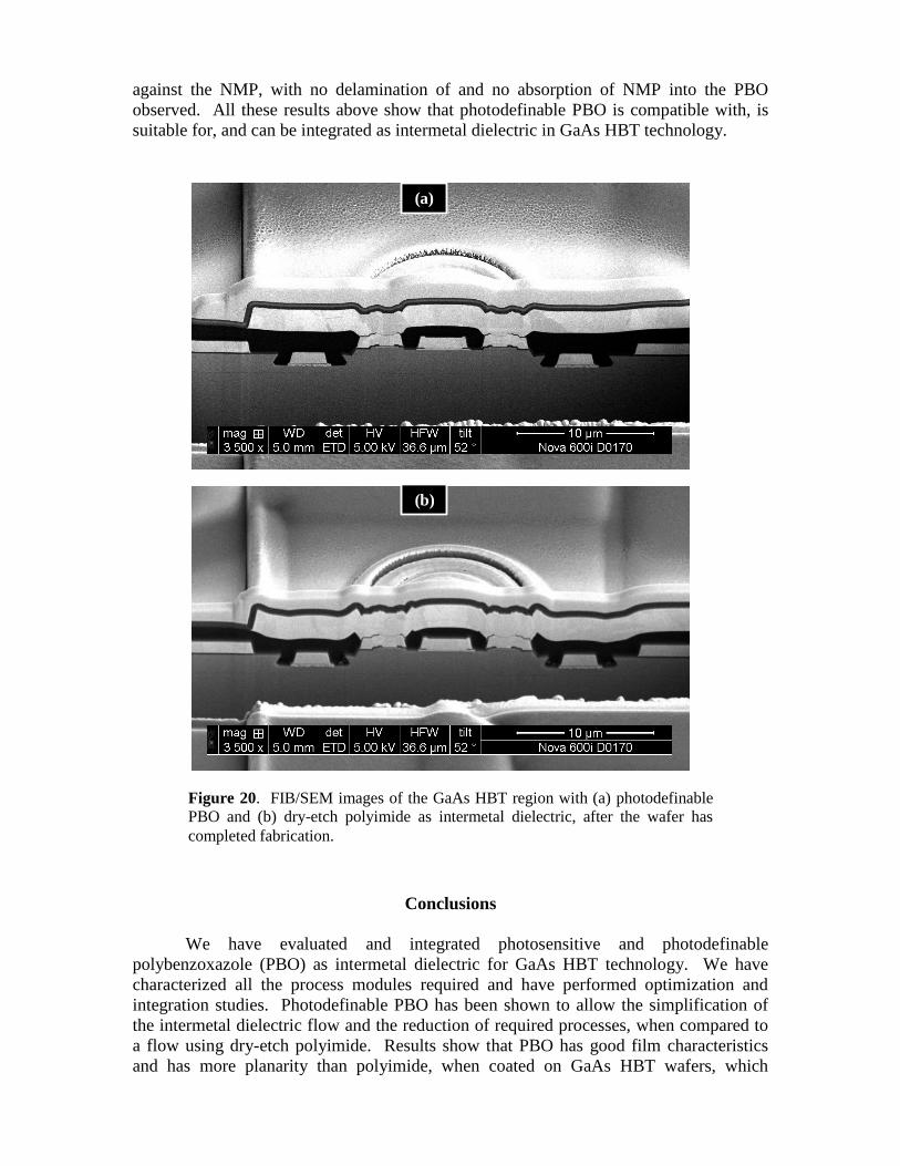
against the NMP, with no delamination of and no absorption of NMP into the PBO
observed. All these results above show that photodefinable PBO is compatible with, is
suitable for, and can be integrated as intermetal dielectric in GaAs HBT technology.
(a)
(b)
Conclusions
We have evaluated and integrated photosensitive and photodefinable
polybenzoxazole (PBO) as intermetal dielectric for GaAs HBT technology. We have
characterized all the process modules required and have performed optimization and
integration studies. Photodefinable PBO has been shown to allow the simplification of
the intermetal dielectric flow and the reduction of required processes, when compared to
a flow using dry-etch polyimide. Results show that PBO has good film characteristics
and has more planarity than polyimide, when coated on GaAs HBT wafers, which
Figure 20. FIB/SEM images of the GaAs HBT region with (a) photodefinable
PBO and (b) dry-etch polyimide as intermetal dielectric, after the wafer has
completed fabrication.

typically has significant topography and thick metal interconnections. The
photolithography processes, including coat, expose, and develop processes, in addition to
cure and ashing processes were optimized to obtain the desired dielectric thickness, the
required via dimension and sidewall profile, and at the same time perform complete
removal of the PBO from the circuit street. All of the above shows that the PBO film is
suitable for and can be integrated as intermetal dielectric in GaAs HBT technology.
Acknowledgments
The authors would like to acknowledge Ravi Ramanathan, Mike Sun, David Tuunanen,
and James Fillon of Skyworks Solutions, and Farhad Kiaei, Noritaka Matsuie, and
Takeharu Motobe of HD MicroSystems, for their help in this study.
References
1. N. Allouti, P. Chausse, C. Aumont, H. Issele, L. Vignoud, N. Rochat, C. Poulain, M.
Gasiglia, C. Sourd, M. Argoud, P. Coudrain, and Y. Troullier, in Proc. 2013 Electron.
Packag. Technol. Conf. (EPTC), pp 27-32 (2013).
2. T. Shinichiro, T. Hsiao, K. Wu , Y.C. Chen , J.S. Wu, J. T. Chung, C.K. Lin, and S.H.
Tsai , in 2012 IEEE Microwave Symposium Digest (MTT), pp. 1-3 (2012).
3. K. Zoschke, T. Fischer, M. Topper, K. Samulewicz, O. Wunsch, J. Roder, M. Lutz,
O. Ehrmann, and H. Reichl, IEEE Trans. Adv. Packag., 33, 398 (2010).
(a)
Metal 1
Metal 2
Via PBO
Polyimide
Metal 2
Via
Metal 1
(b)
(a)
Metal 2
Metal 2
PBO
Polyimide
Metal 1
Metal 1
(b)
Figure 22. FIB/SEM images of Metal 1
interconnection serpentines with (a) PBO
and (b) polyimide as intermetal dielectric,
after the GaAs wafer has completed
fabrication.
Figure 21. FIB/SEM images of a via on a
low topography location with (a) PBO and
(b) polyimide as intermetal dielectric, after
the GaAs wafer has completed fabrication.
4. M. Topper, T. Fischer, T. Baumgartner, and H. Reichl, in Proc. 60th
Electron. Comp.
Technol. Conf. (ECTC), pp. 769-776 (2010).
5. J. Yota, H. Ly, R. Ramanathan, H.-C. Sun, D. Barone, T. Nguyen, K. Katoh, M. Ohe,
R.L. Hubbard, and K. Hicks, IEEE Trans. Semicond. Manuf., 20 (3), 323 (2007).
6. H.S. Noh, K.S. Moon, A. Cannon, P.J. Hesketh, and C.P. Wong, J. Micromech.
Microengr., 13, 625 (2004).
7. J. Yota, H. Ly, D. Barone, M. Sun, and R. Ramanathan, in 2008 Int. Conf. on
Compound Semicond. Manufact. Technol. (CS MANTECH) Digest, pp. 103-106
(2008).
8. M. Kojima, H. Sekine, H. Suzuki, H. Satou, D. Makino, F. Kataoka, J. Tanaka, and F.
Shouji, in Proc. 39th
Electron. Comp. Conf., pp. 920–924 (1989).
9. A.J.G. Strandjord, W.J. Rogers, Y. Ida, R.R. DeVeillis, S. Shiau, E.S. Moyer, D.M.
Scheck, and P.E. Garrou, in Proc. 47th
Electron. Comp. Technol. Conf., pp. 1260–
1268 (1997).
10. P.E. Ganrou, W.B. Rogers, D.M. Scheck, A.J.G. Strandjord, Y. Ida, and K. Ohba,
IEEE Trans. Adv. Packag., 22, 487 (1999).
11. M.E. Mills, P. Townsend, D. Castillo, S. Martin and A. Achen, Microelectron. Eng.,
33, 327 (1997).
12. P. Garrou, D. Scheck, J. Im, J. Hetzner, G. Meyers, D. Hawn, J. Wu, M. Vincent, and
C.P. Wong, IEEE Trans. Adv. Packag., 23, 568 (2000).
13. D. Barone, J. Yota, H. Ly, S. Mui, S. Tiku, and S. Canale, in 2008 Int. Conf. on
Compound Semicond. Manufact. Technol. (CS MANTECH) Digest, pp. 57-60 (2008).
14. S.L. Hsu, C.Y.Lin, and S.W. Chuang, J. Appl. Polym. Sci., 97, 2350 (2005).
15. R. Yu, T. Tai, A. Hsieh, A. Cheng, I. Tseng, M. Tsai, H. Tong, and J. Lee, in Proc.
29th
Int. Electron. Manuf. Technol. Symp., pp. 5-9. (2004).
16. S. Luo and C.P. Wong, in 2002 Proc. Electron. Comp. Technol. Conf., pp. 1390-1395
(2002).
17. H. Matsutani, T. Hattori, M. Ohe, T. Ueno, R.L. Hubbard, and Z. Fathi, J.
Photopolym. Sci. Technol., 18, 327 (2005).
18. R.V. Tanikella, S.A. Bidstrup Allen, and P.A. Kohl, J. Appl. Polymer Sci., 83,
3055(2002).
19. S. Wolf and R.N. Tauber, Silicon Processing for the VLSI Era Volume 1 - Process
Technology, Lattice Press, Sunset Beach (1986).
20. J. Yota, K. Kwok, and R. Ramanathan, in 2014 Int. Conf. on Compound Semicond.
Manufact. Technol. (CS MANTECH) Digest, pp. 163-166 (2014).
21. J. Yota, H. Shen, and R. Ramanathan, J. Vac. Sci Technol. A, 31, 01A134-1 (2012).
22. S.K. Gandhi, VLSI Fabrication Principles, Silicon and Gallium Arsenide, New York,
John Wiley (1983).
23. W. Liu, Handbook of III-V Heterojunction Bipolar Transistors, New York, John
Wiley (1998).
24. R. Williams, Modern GaAs Processing Methods, Artech House, Boston (1990).
25. B. Mimoun, H. T. M. Pham, V. Henneken, and R. Dekker, J. Vac. Sci. Technol. B, 31,
021201 (2013).
26. J.F. Zheng, H. Demir, V.A. Sabnis, O. Fidaner, J.S. Harris, and D.A.B. Miller, J. Vac.
Sci. Technol. B, 24, 1117 (2006).
27. J. Yota, J. Electrochem. Soc. 156, G173 (2009).
28. J. Yota, ECS Trans., 53, 281 (2013).
29. W.S. Shih, J. Yota, and K. Itchhaporia, J. Electrochem. Soc., 155, G65 (2008).

30. S. Wolf, Silicon Processing for the VLSI Era Volume 4 - Deep-Submicron Process
Technology, Lattice Press, Sunset Beach (2002).
31. E. Takeuchi, T. Takeda, and T. Hirano, in Proc. Electron. Comp. Technol. Conf., pp.
818-823 (1990).
32. J. J. Reche and D.H. Kim, Microelectron. Rel., 43, 879 (2003).
33. P.J. Zampardi, C. Cismaru, H. Banbrook, and B. Li, Microelectron. Rel., 52, 2870
(2012).
34. B. Rogers, D. Scheck, and P. Garrou, in Proc. 3rd Int. Symp. Adv. Packag. Mater.,
pp. 15-18 (1997).
35. P. Garrou, in Proc. 4th
Int. Symp. Adv. Packag. Mater., pp. 53-59 (1998).


