
ii
SYNTHESIS AND CHARACTERIZATION OF OXIDE CONDUCTORS IN
PbO-Bi2O3-M2O5 (M = V, P, As)
LEE CHIU SZE
DOCTOR OF PHILOSOPHY
UNIVERSITI PUTRA MALAYSIA
2004

iii
SYNTHESIS AND CHARACTERIZATION OF OXIDE CONDUCTORS IN
PbO-Bi2O3-M2O5 (M = V, P, As)
By
LEE CHIU SZE
Thesis Submitted to the School of Graduate Studies, Universiti Putra Malaysia,
in Fulfilment of the Requirements for the Degree of Doctor of Philosophy
April 2004

iv
Abstract of thesis presented to the Senate of Universiti Putra Malaysia in fulfilment of the requirements for the degree of Doctor of Philosophy
SYNTHESIS AND CHARACTERIZATION OF OXIDE CONDUCTORS IN
PbO-Bi2O3-M2O5 (M = V, P, As)
By
LEE CHIU SZE
April 2004
Chairperson: Professor Lee Chnoong Kheng, Ph.D.
Faculty: Science and Environmental Studies
Materials of compositions PbBi6M2O15 and (PbO)n(BiMO4), where M = V, P, As and
n = 1, 2, 4 were prepared via solid state reaction. These materials were characterised
using X-ray diffraction (XRD), density measurement, inductively coupled plasma-
atomic emission spectrometry (ICP-AES), ac impedance spectroscopy, differential
thermal analysis (DTA), thermogravimetry analysis (TGA), Fourier-transform
infrared spectroscopy (FT-IR) and scanning electron microscopy (SEM).
Complete solid solution series were obtained in the PbBi6V2O15-PbBi6P2O15,
PbBi6V2O15-PbBi6As2O15 and PbBi6P2O15-PbBi6As2O15 systems. All the materials
were isostructural, and crystallised in orthorhombic symmetry. However, the cell
parameter a of these materials was twice those reported in JCPDS. The conductivity
of these materials decreased in the order of PbBi6V2O15 > PbBi6As2O15 >
PbBi6P2O15. PbBi6V2O15 is an oxide ion conductor as it has a transference number of
0.8 above 650ºC.

v
Substitution of Sr for Pb in PbBi6V2O15 resulted in the formation a new material of
SrBi6V2O15 with higher conductivity. On the other hand, Pb in both PbBi6V2O15 and
PbBi6As2O15 could be replaced by Na and Bi, resulting in the formation of
NaBi13V4O30 and NaBi13As4O30. Besides successfully suppressing the phase
transition observed in PbBi6V2O15, these materials had higher conductivity compared
to that of PbBi6(V/As)2O15. The conductivity of these materials was in the range of ~
10-3 ohm-1 cm-1 at 800°C. Conductivity decreased in the order of NaBi13V4O30 >
SrBi6V2O15 > PbBi6V2O15. These materials appeared to be oxide ion conductors.
Complete solid solution series were formed in the Pb2BiPO6-Pb2BiAsO6, Pb4BiPO8-
Pb4BiVO8, Pb4BiPO8-Pb4BiAsO8 and Pb4BiVO8-Pb4BiAsO8 systems. The properties
determined generally agreed with those reported; these materials were mixed oxide
ion conductors. The conductivity decreased in the order of Pb2BiMO6 > PbBiMO5 >
Pb4BiMO8, and V > As > P.

vi
Abstrak tesis yang dikemukakan kepada Senat Universiti Putra Malaysia sebagai memenuhi keperluan untuk ijazah kedoktoran
SINTESIS DAN PENCIRIAN KONDUKTOR OKSIDA DALAM
PbO-Bi2O3-M2O5 (M = V, P, As)
Oleh
LEE CHIU SZE
April 2004
Pengerusi: Profesor Lee Chnoong Kheng, Ph.D.
Fakulti: Sains and Pengajian Alam Sekitar
Bahan-bahan dengan komposisi PbBi6M2O15 dan (PbO)n(BiMO4), di mana M = V, P,
As dan n = 1, 2, 4 telah disediakan melalui tindak balas keadaan pepejal. Bahan-
bahan telah dicirikan dengan mengunakan pembelauan sinar-X (XRD), pengukuran
ketumpatan, plasma aruhan keduaan-spektroskopi penyebaran atom (ICP-AES),
spektroskopi impedans ac, analisis perbezaan terma (DTA), analisis termogravimetri
(TGA), spektroskopi inframerah transformasi Fourier (FT-IR) dan spektroskopi
imbasan electron (SEM).
Larutan pepejal lengkap telah diperolehi dalam sistem PbBi6V2O15-PbBi6P2O15,
PbBi6V2O15-PbBi6As2O15 dan PbBi6P2O15-PbBi6As2O15. Semua bahan mempunyai
simetri yang sama, dan mereka dihablurkan dalam simetri ortorombik. Tetapi,
parameter unit cell a bahan-bahan ini adalah dua kali ganda daripada yang dilaporkan
dalam JCPDS. Kekonduksian bahan-bahan ini menurun dalam susunan PbBi6V2O15
> PbBi6As2O15 > PbBi6P2O15. PbBi6V2O15 adalah konduktor ion oksida disebabkan ia
mempunyai nombor pindahan 0.8 pada suhu 650ºC ke atas.

vii
Pertukaran Sr untuk Pb dalam PbBi6V2O15 telah menghasilkan pembentukan satu
bahan baru SrBi6V2O15 dengan kekonduksian yang lebih tinggi. Selain itu, Pb dalam
PbBi6V2O15 and PbBi6As2O15 boleh diganti dengan Na dan Bi, mengakibatkan
panghasilan NaBi13V4O30 dan NaBi13As4O30. Selain daripada berjaya menghilangkan
peralihan fasa yang dilihat dalam PbBi6V2O15, bahan-bahan ini mempunyai
kekonduksian yang lebih tinggi daripada PbBi6(V/As)2O15. Kekonduksian bahan-
bahan ini adalah dalam lingkungan ~ 10-3 ohm-1 cm-1 pada suhu 800°C.
Kekonduksian menurun dalam susunan NaBi13V4O30 > SrBi6V2O15 > PbBi6V2O15.
Bahan-bahan ini merupakan konduktor ion oksida.
Larutan pepejal lengkap telah dibentuk dalam sistem Pb2BiPO6-Pb2BiAsO6,
Pb4BiPO8-Pb4BiVO8, Pb4BiPO8-Pb4BiAsO8 dan Pb4BiVO8-Pb4BiAsO8. Kelakuan
yang ditentukan adalah agak sama dengan yang dilaporkan; bahan-bahan ini
merupakan konduktor campuran ion oksida. Kekonduksian menurun dalam susunan
Pb2BiMO6 > PbBiMO5 > Pb4BiMO8, dan V > As > P.

viii
ACKNOWLEDGEMENTS
First of all I would like to express my deep gratitude to my supervisor, Professor Dr.
Lee Chnoong Kheng, for her constant encouragement, constructive suggestions and
continuous discussion throughout the project. I would also like to extend my sincere
appreciation to my co-supervisors Assoc. Prof. Dr. Zulkarnain Zainal and Assoc.
Prof. Dr. Mansor Hashim for their guidance, suggestions and comments throughout
the research work.
My special thanks are due to Professor Dr. A. R. West for helpful discussions and
comments on this work. Besides, I would also like to thank Dr. Akiteru Watanabe for
his assistance in carrying out the transference number measurements.
Particular thanks are also extended to Madam Choo (ICP-AES), Mr. Kamal Margona
(DTA, TGA), Mdm. Rusnani Amirudin (IR), Mr. Ho Oi Kuan, Mrs. Azilah Ab. Jalil,
Mr. Rafiez (SEM) and all the laboratory technicians for their help and guidance in
operating the instruments.
I am extremely grateful to all my friends, Miss Lim Ei Bee, Miss Sim Leng Tze,
Miss Lee Siew Ling, lab mates and all my friends in UPM for their constant
encouragements and help throughout these few years.
The financial support from the Ministry of Science and Technology and Universiti
Putra Malaysia is gratefully acknowledged. Without this support, it is impossible for

ix
me to pursue this project with success. Lastly, I would also like to extend my
gratitude to the Malaysian government for granting me the PASCA scholarship.
Last but not least, I would like to give my sincere thanks to all the members of my
family and Dr. Lim Kean Pah for their love, continuous support, encouragement and
understanding.

x
LIST OF ABBREVIATIONS / NOTATIONS / GLOSSARY OF TERMS
3D three dimensions ac alternating current BIMEVOX bismuth metal vanadium oxide dc direct current DTA differential thermal analysis FT-IR Fourier-transform infrared spectroscopy ICDD international centre for diffraction data ICP-AES inductively coupled plasma-atomic emission spectrometry JCPDS Joint Committee on Powder Diffraction Standards µPDSM micro powder diffraction search / match SEM scanning electron microscopy SOFC solid oxide fuel cell TGA thermogravimetry analysis XRD X-ray diffraction YSZ yittria stabilised zirconia a, b, c, α, β, γ lattice constant A area Aw Warburg coefficient C capacitance Cb bulk capacitance Cdl double-layer capacitance Cgb grain boundary capacitance Co vacuum capacitance

xi
d d-spacing D density e charge of the conducting species eo permittivity of free space E electric field Ea activation energy ε' relative permittivity ε* complex permittivity f frequency F Faraday constant h, k, l Miller indice I current j flux of charge J density of the current l thickness λ wavelength M dopant introduced M’ real part of modulus M” imaginary part of modulus M* complex modulus µ mobility of the species P’ partial pressure to be measured P” reference partial pressure R resistance

xii
R universal gas constant Rb bulk resistance Rgb grain boundary resistance σ conductivity t transference number T temperature θ Bragg angle τ electrical relaxation times ω angular frequency Z formula unit Z impedance Z’ real part of impedance Z” imaginary part of impedance Z* complex impedance

xiii
TABLE OF CONTENTS
Page
ABSTRACT ABSTRAK ACKNOWLEDGEDEMENTS APPROVAL DECLARATION LIST OF TABLES LIST OF FIGURES LIST OF ABBREVIATIONS / NOTATIONS / GLOSSARY OF TERMS
ii iv vi viii x xiv xvii xxx
CHAPTER
1 INTRODUCTION
1.1 Ionic Conductivity and Solid Electrolytes 1.1.1 Ionic Conduction
1.2 Solid Solutions 1.3 Oxide Ion Conductors and Their Applications
1.3.1 Oxygen Sensors 1.3.2 Solid Oxide Fuel Cell (SOFC)
1.4 Objectives
1.1 1.3 1.6 1.7 1.8 1.10 1.14
2 LITERATURE REVIEW 2.1 Oxide Ion Conductors 2.2 Pure Bismuth Oxide 2.3 Bi2O3-based Binary Systems 2.4 Bi2O3-based Ternary Systems
2.1 2.2 2.7 2.14
3 MATERIALS AND METHODS 3.1 Sample Preparation
3.1.1 PbBi6(V/P/As)2O15, Pb1-xSrxBi6(V/As)2O15 and NaBi13(V/P/As)4O30 Solid Solutions
3.1.2 PbBi(V/As)O5, Pb1-xSrxBiVO5, Pb2Bi(V/P/As)O6 and Pb4Bi(V/P/As)O8 Solid Solutions
3.2 Analysis and Characterisation 3.2.1 X-ray Diffraction (XRD) 3.2.2 Density Measurement 3.2.3 Elemental Analysis – Inductively Coupled Plasma-
Atomic Emission Spectrometry (ICP-AES) 3.2.4 Electrical Properties 3.2.5 Thermal Analysis 3.2.6 Fourier-transform Infrared Spectroscopy (FT-IR)
3.1 3.1 3.3 3.6 3.6 3.10 3.11 3.14 3.27 3.29

xiv
3.2.7 Scanning Electron Microscopy (SEM) 3.3 Phase Stability
3.3.1 Melting Point 3.3.2 Slow Cool
3.30 3.31 3.31 3.31
4 RESULTS AND DISCUSSION 4.1 PbBi6(V/P/As)2O15 Solid Solutions
4.1.1 Phase Purity 4.1.2 Density 4.1.3 Melting Point and Phase Stability 4.1.4 Elemental Analysis – ICP-AES 4.1.5 Fourier-transform Infrared Spectroscopy 4.1.6 Thermal Analysis 4.1.7 Scanning Electron Microscopy 4.1.8 Electrical Properties
4.2 Pb1-xSrxBi6(V/As)2O15 Solid Solutions 4.2.1 Phase Purity 4.2.2 Density 4.2.3 Melting Point and Phase Stability 4.2.4 Elemental Analysis – ICP-AES 4.2.5 Fourier-transform Infrared Spectroscopy 4.2.6 Thermal Analysis 4.2.7 Scanning Electron Microscopy 4.2.8 Electrical Properties
4.3 NaBi13(V/P/As)4O30 Solid Solutions 4.3.1 Phase Purity 4.3.2 Density 4.3.3 Melting Point and Phase Stability 4.3.4 Elemental Analysis – ICP-AES 4.3.5 Fourier-transform Infrared Spectroscopy) 4.3.6 Thermal Analysis 4.3.7 Scanning Electron Microscopy 4.3.8 Electrical Properties
4.4 (PbO)n[Bi(V/As)O4], n = 1, and Their Solid Solutions 4.4.1 Phase Purity and Crystal Structure 4.4.2 Melting Point and Phase Stability 4.4.3 Elemental Analysis – ICP-AES 4.4.4 Fourier-transform Infrared Spectroscopy 4.4.5 Thermal Analysis 4.4.6 Scanning Electron Microscopy 4.4.7 Electrical Properties
4.5 (PbO)n[Bi(V/P/As)O4], n = 2, and Their Solid Solutions 4.5.1 Phase Purity and Crystal Structure 4.5.2 Density 4.5.3 Melting Point and Phase Stability 4.5.4 Elemental Analysis – ICP-AES 4.5.5 Fourier-transform Infrared Spectroscopy 4.5.6 Thermal Analysis
4.1 4.1 4.11 4.11 4.15 4.19 4.23 4.29 4.32 4.54 4.54 4.60 4.63 4.63 4.65 4.65 4.67 4.69 4.82 4.82 4.88 4.88 4.93 4.94 4.96 4.96 4.100 4.118 4.118 4.123 4.126 4.126 4.128 4.128 4.128 4.142 4.142 4.150 4.155 4.156 4.156 4.161

xv
4.5.7 Scanning Electron Microscopy 4.5.8 Electrical Properties
4.6 (PbO)n[Bi(V/P/As)O4], n = 4, and Their Solid Solutions 4.6.1 Phase Purity and Crystal Structure 4.6.2 Density 4.6.3 Melting Point and Phase Stability 4.6.4 Elemental Analysis – ICP-AES 4.6.5 Fourier-transform Infrared Spectroscopy 4.6.6 Thermal Analysis 4.6.7 Scanning Electron Microscopy 4.6.8 Electrical Properties
4.7 Summary
4.165 4.168 4.183 4.183 4.191 4.191 4.198 4.198 4.203 4.203 4.205 4.219
5 CONCLUSIONS
5.1
REFERENCES R.1 APPENDICES A.1 BIODATA OF THE AUTHOR B.1

xvi
LIST OF TABLES
Table Page
3.1 List of samples prepared in PbBi6(V/As)2O15, Pb1-x
SrxBi6(V/As)2O15 and NaBi13(V/P/As)4O30 solid solution series
3.2
3.2 List of samples prepared in PbBi(V/As)O5, Pb1-xSrxBiVO5, Pb2Bi(V/P/As)O6 and Pb4Bi(V/P/As)O8 solid solution series
3.5
3.3 Wavelength used and detection limit for each element in the
elemental analysis by ICP-AES
3.13
3.4 Capacitance values and their possible interpretation (Irvine et al., 1990)
3.21
4.1 Melting points of x in PbBi6V2-xPxO15, PbBi6V2-xAsxO15 and
PbBi6P2-xAsxO15 solid solutions
4.15
4.2 Atomic % of the elements calculated from ICP-AES analysis of PbBi6V2O15, PbBi6P2O15 and PbBi6As2O15
4.16
4.3 Atomic % of the elements determined from ICP-AES analysis
of selected samples in PbBi6V2-xPxO15 solid solutions
4.17
4.4 Atomic % of the elements determined from ICP-AES analysis of selected samples in PbBi6V2-xAsxO15 solid solutions
4.18
4.5 Atomic % of the elements determined from ICP-AES analysis
of selected samples in PbBi6P2-xAsxO15 solid solutions
4.19
4.6 Vibrational frequencies for M-O stretching (Nakamoto, 1970) 4.23
4.7 Phase transition temperatures of x in PbBi6V2-xPxO15 4.28
4.8 Phase transition temperatures of x in PbBi6V2-xAsxO15 4.29
4.9 Phase transition temperatures of x in PbBi6P2-xAsxO15 4.29
4.10 Grain size of x in PbBi6V2-xPxO15 4.31
4.11 Grain size of x in PbBi6V2-xAsxO15 4.32
4.12 Conductivity values at 550 and 800°C and the activation energy for PbBi6P2O15 at different atmospheres
4.46
4.13 Conductivity values at 550 and 800°C and the activation energy
for PbBi6As2O15 at different atmospheres
4.46

xvii
4.14 First 30 lines of the indexed X-ray diffraction pattern for orthorhombic SrBi6V2O15 with a = 23.9122(4) Å, b = 17.1561(3) Å, c = 11.1001(2) Å and α = β = γ = 90º, V = 4553.733(237) Å3
4.56
4.15 Synthesis temperatures of x in Pb1-xSrxBi6As2O15 4.60
4.16 Melting points of x in Pb1-xSrxBi6V2O15 4.63
4.17 Atomic % of the elements determined from ICP-AES analysis of selected samples in Pb1-xSrxBi6V2O15 solid solutions
4.64
4.18 Grain size of Pb1-xSrxBi6V2O15 4.67
4.19 Grain size of Pb1-xSrxBi6As2O15 4.69
4.20 Melting points of x in NaBi13V4-xAsxO30 4.92
4.21 Melting points of x in NaBi13As4-xPxO30 4.92
4.22 Melting points of x in NaBi13V4-xPxO30 4.93
4.23 Atomic % of the elements determined from ICP-AES analysis
of selected samples in NaBi13V4-xAsxO30 solid solutions
4.93
4.24 Grain size of NaBi13V4O30 and NaBi13As4O30 4.98
4.25 Grain size of x in NaBi13V4-xAsxO30 4.98
4.26 Grain size of x in NaBi13V4-xPxO30 4.98
4.27 Melting points of x in PbBiV2-xAsxO5 4.123
4.28 Atomic % of the elements determined from ICP-AES analysis of PbBi(V/As)O5
4.126
4.29 Crystallographic data of different phases of Pb2BiVO6 (Mizrahi
et al., 1995)
4.142
4.30 Melting points of Pb2BiP1-xVxO6 solid solutions 4.155
4.31 Melting points of Pb2BiP1-xAsxO6 solid solutions 4.155
4.32 Melting points of Pb2BiV1-xAsxO6 solid solutions 4.156
4.33 Atomic % of the elements determined from ICP-AES analysis of Pb2Bi(V/P/As)O6
4.157

xviii
4.34 DTA transitions of Pb2BiP1-xVxO6, Pb2BiV1-xAsxO6 and Pb2BiP1-xAsxO6 solid solutions
4.163
4.35 Grain size of x in Pb2BiP1-xVxO6 4.167
4.36 Grain size of x in Pb2BiV1-xAsxO6 4.167
4.37 Grain size of x in Pb2BiP1-xAsxO6 4.168
4.38 Cell parameters of Pb4BiVO8, Pb4BiPO8 and Pb4BiAsO8 and
reported values
4.188
4.39 Melting points of Pb4BiP1-xVxO8, Pb4BiV1-xAsxO8 and Pb4Bi P1-xAsxO8 solid solutions
4.198
4.40 Atomic % of the elements determined from ICP-AES analysis
of Pb4Bi(V/P/As)O8
4.199

xix
CHAPTER 1
INTRODUCTION
1.1 Ionic Conductivity and Solid Electrolytes
Electrical conduction in solid materials usually occurs by the long range diffusion of
either electrons or ions. This has therefore created many different characteristics of
electrical conductivity, such as metallic conductivity, superconductivity,
semiconductivity and ionic conductivity.
Ionic conductivity occurs in materials known variously as solid electrolytes,
superionic conductors or fast ion conductors. Many of the crystalline materials such
as NaCl or MgO, have low ionic conductivities because the atoms or ions can only
vibrate at their atomic positions. However, solid electrolytes are an exception. Solid
electrolytes usually have freely moving cations (e.g. H+, Na+, Li+, Ag+) or anions
(e.g. O2-, F-) that move throughout the crystalline structure.
Figure 1.1 shows the different types of electrical conductivities and examples of the
different materials. Solid electrolytes have conductivities that fall between that of the
semiconductor and aqueous electrolyte.
Solid electrolytes are, therefore, intermediate between normal crystalline solids with
regular three dimensional structures as well as immobile atoms or ions and liquid
electrolytes, which do not have regular structures but mobile ions. This characteristic
is supported by data on the relative entropies of polymorphic transitions and melting.

xx
Figure 1.1: Electrical conductivities of selected common substances and representative solid electrolytes (Greenblatt, 1994)
Solid electrolytes are often stable only at high temperatures. At low temperatures,
they may undergo a phase transition to give a polymorph with a low ionic
conductivity and a more usual type of crystalline structure (Figure 1.2). Besides,
solid electrolytes may also form as a consequence of a gradual increase in defect
concentration with increasing temperature.
Figure 1.2: Solid electrolytes as intermediate between normal crystalline solids and liquids (West, 1999)
Normal crystalline
solid
Incresing defect
concentration
Solid electrolyte Liquid
Phase transition
Temperature

xxi
Intensive research has been carried out on solid electrolytes in recent years as these
materials offer a wide range of potential technological applications, such as high-
energy-density batteries, fuel cells, sensors, electrochromic materials for both optical
display and ‘smart window’ devices, low-cost electrolysis of water and selective
atomic filter. Some of these devices are available commercially. For example,
oxygen detectors for automotive pollution-control systems employ solid O2-
conductors and Li+ batteries for electronic equipment.
1.1.1 Ionic Conduction
The electrical conductivity is defined as the constant of proportionality between the
flux j of charge and the electric field, E
j = σE (1.1)
If
j = eiJ (1.2)
with ei = charge of the conducting species, i
J = density of the current
and
Ei
in
J=µ (1.3)
where µi = mobility of the species
ni = number of charge carrier
therefore, for any material and charge carrier, the specific conductivity is given by
∑=i
iii µenσ (1.4)

xxii
For ionic conductivity,
σ = Nioneµion (1.5)
where Nion = number of ions which can change their position under the influence of
an electric field
µion = the mobility of these ions
(Elliott, 1998; West, 1999)
In order for the ions to move through a crystalline solid, they must have sufficient
energy to pass over an energy barrier and there must be empty lattice sites for the
ions to jump into. Thus, for an intrinsic conduction, Nion depends on the vacancy
concentration caused by Schottky or Frenkel defects.
Transference number, ti is defined as the ratio of the partial current generated by
migration of species i to the total current generated by all conductive species.
Therefore,
∑
=
ii
ii
σ
σt (1.6)
For an ideal ionic conductor, transference number ti = 1 (Kudo and Fueki, 1989).
Conductivities are usually temperature dependent, and for all materials, except
metals, the conductivity increases with increasing temperature.
xxiii
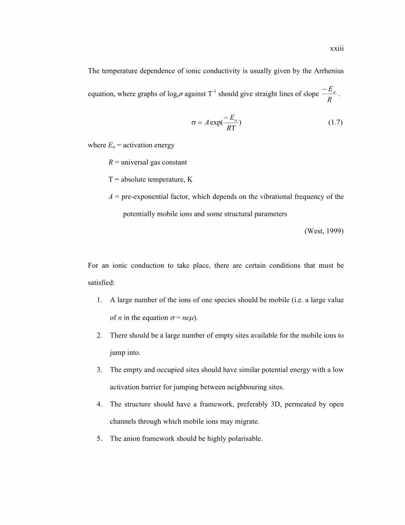
The temperature dependence of ionic conductivity is usually given by the Arrhenius
equation, where graphs of logeσ against T-1 should give straight lines of slope R
Ea−.
)T
exp(R
EA a−
=σ (1.7)
where Ea = activation energy
R = universal gas constant
T = absolute temperature, K
A = pre-exponential factor, which depends on the vibrational frequency of the
potentially mobile ions and some structural parameters
(West, 1999)
For an ionic conduction to take place, there are certain conditions that must be
satisfied:
1. A large number of the ions of one species should be mobile (i.e. a large value
of n in the equation σ = neµ).
2. There should be a large number of empty sites available for the mobile ions to
jump into.
3. The empty and occupied sites should have similar potential energy with a low
activation barrier for jumping between neighbouring sites.
4. The structure should have a framework, preferably 3D, permeated by open
channels through which mobile ions may migrate.
5. The anion framework should be highly polarisable.

xxiv
Even when all these conditions are met, the ionic conduction may still be affected by
microstructural factors such as grain boundaries, grain size, pores size and between
grain-grain contact. However, these effects have not been studied experimentally in
great detail.
1.2 Solid Solutions
A solid solution is basically a crystalline phase that can have variable composition.
As with doped crystals, simple solid solutions are divided into two types:
substitutional solid solutions in which the atom or ion that is being introduced
directly replaces an atom or ion in the parent structure and interstitial solid solutions
in which the introduced species occupies a site that is normally empty and no ions or
atoms are left out.
Doping is an important mechanism in preparing solid solutions. Usually, doping with
aliovalent cations (the substituted ions are ions of different charge) will result in
creation of vacancies or interstitials (ionic compensation) or electrons or holes
(electronic compensation). Therefore, substituting a cation of lower valence may
result in creating anion vacancies, thus, increasing the oxygen vacancies in the oxide
ion conductor and consequently increasing the conductivity.
In solid solution formation, ions of similar size may substitute for each other easily
and extensive solid solutions could form which are stable at all temperatures; the
enthalpy of mixing of such similar-sized ions is likely to be small and the driving
force for solid solution formation is the increased entropy. Solid solutions may form

xxv
at high temperatures if substituting ions differ in size by 15 to 20%, where the
entropy term is able to offset the positive enthalpy term. With ions that differ in size
by more that ~ 30%, however, solid solutions are normally not expected to form.
Solid solution formation is very temperature dependent. Thus, extensive solid
solutions often form at high temperatures whereas at lower temperatures, these may
be more restricted or practically non-existent.
In order to form a complete solid solution, it is essential that the end members are
isostructural; however, the reverse is not necessarily true.
1.3 Oxide Ion Conductors and Their Applications
A very interesting subgroup of solid electrolytes is the materials that display oxygen
ion conductivity, known as oxide ion conductors, where the oxide ions are the charge
carriers.
Oxide ion conductors have been with us for over a century. The first application was
by Nerst in around 1900, who used stabilised zirconia as filaments in his
revolutionary ‘glower’ electric lights, driven by the need to replace dirty and
dangerous candles and gas lamps. Remarkably, the same basic material, now known
as yttria-stabilised zirconia, is the key solid electrolyte component currently in
various solid oxide fuel cell and sensor applications.


