ULN2003A
1
HIGH VOLTAGE AND HIGH CURRENT DARLINGTON TRANSISTOR ARRAY
DESCRIPTION
The ULN2003A is a monolithic high voltage and high current
Darlington transistor arrays. It consists of seven NPN darlington
pairs that features high-voltage outputs with common-cathode
clamp diode for switching inductive loads. The collector-current
rating of a single darlington pair is 500mA. The darlington pairs
may be parrlleled for higher current capability. Applications include
relay drivers,hammer drivers, lampdrivers,display drivers(LED gas
discharge),line drivers, and logic buffers.
The ULN2003A has a 2.7k ? series base resistor for each
darlington pair for operation directly with TTL or 5V CMOS
devices.
FEATURES
* 500mA rated collector current(Single output)
* High-voltage outputs: 50V
* Inputs compatibale with various types of logic.
* Relay driver application
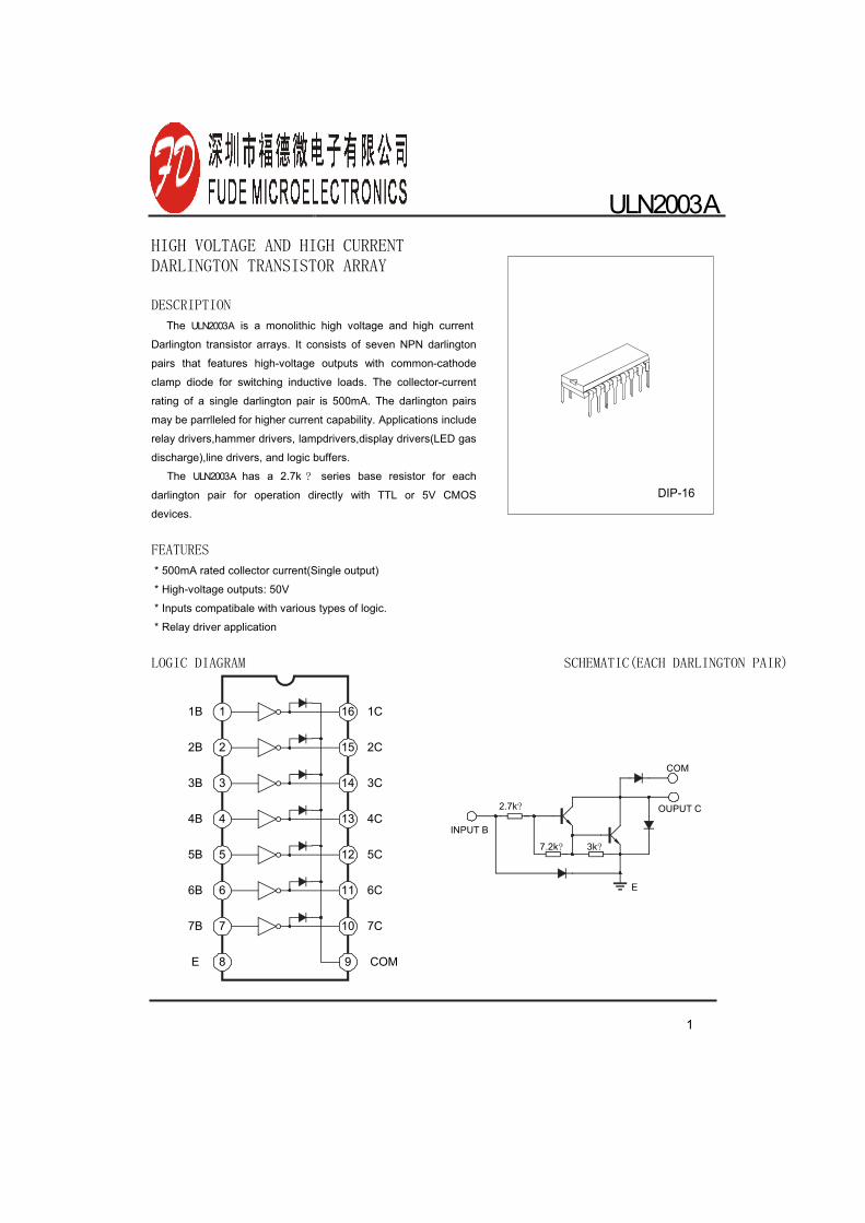
DIP-16
LOGIC DIAGRAM SCHEMATIC(EACH DARLINGTON PAIR)
1
2
3
4
5
6
7
8
16
15
14
13
12
11
10
9
1B
2B
3B
4B
5B
6B
7B
E
1C
2C
3C
4C
5C
6C
7C
COM
INPUT B
OUPUT C
COM
E
7.2k? 3k?
2.7k?
ULN2003A
2
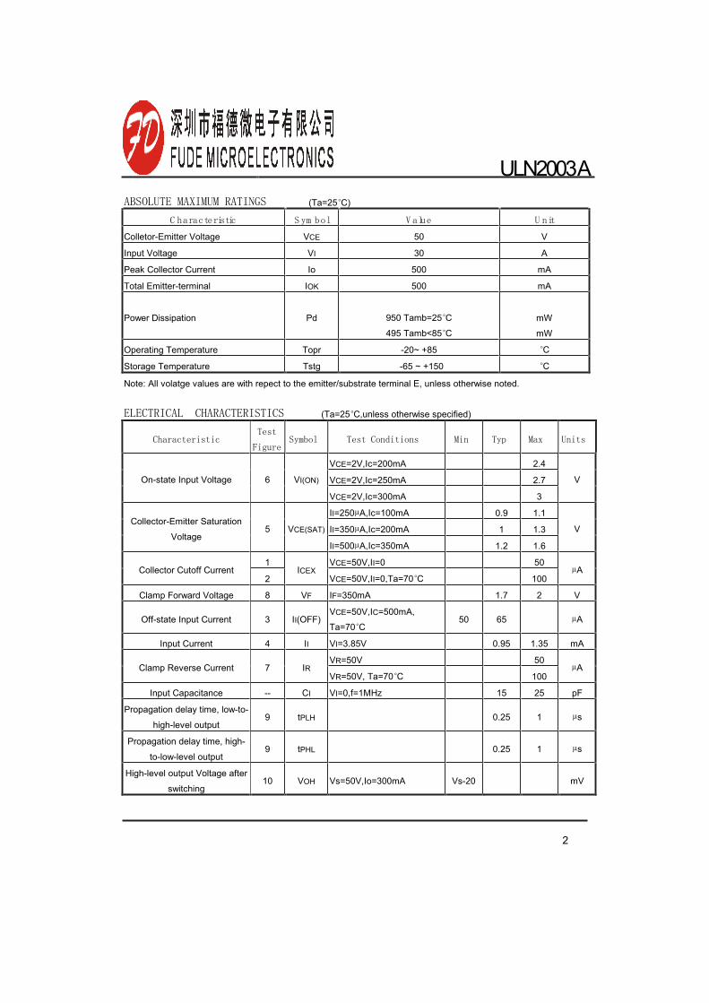
ABSOLUTE MAXIMUM RATINGS (Ta=25°C)
tinU eulaV lobmyS citsiretcarahC
Colletor-Emitter Voltage VCE V05
VegatloVtupnI I A03
Am005oItnerruCrotcelloCkaeP
Ilanimret-rettimElatoT OK Am005
dPnoitapissiDrewoP 950 Tamb=25°C
495 Tamb<85°C
mW
mW
Operating Temperature Topr -20~ +85 °C
051+~56-gtsTerutarepmeTegarotS °C
Note: All volatge values are with repect to the emitter/substrate terminal E, unless otherwise noted.
ELECTRICAL CHARACTERISTICS (Ta=25°C,unless otherwise specified)
Characteristic Test
Figure Symbol Test Conditions Min Typ Max Units
VCE 4.2Am002=cI,V2=
VCE 7.2Am052=cI,V2=On-state Input Voltage 6 VI(ON)
VCE 3Am003=cI,V2=
V
II=250µA,Ic=100mA 0.9 1.1
II=350µA,Ic=200mA 1 1.3Collector-Emitter Saturation
Voltage5 VCE(SAT)
II=500µA,Ic=350mA 1.2 1.6
V
1 VCE=50V,II 050=Collector Cutoff Current
2ICEX
VCE=50V,II=0,Ta=70°C 100µA
Clamp Forward Voltage 8 VF IF V27.1Am053=
Off-state Input Current 3 II(OFF)VCE=50V,IC=500mA,
Ta=70°C50 65 µA
Input Current 4 II VI Am53.159.0V58.3=
VR 05V05=Clamp Reverse Current 7 IR
VR=50V, Ta=70°C 100µA
Input Capacitance -- CI VI Fp5251zHM1=f,0=
Propagation delay time, low-to-
high-level output9 tPLH 0.25 1 µs
Propagation delay time, high-
to-low-level output9 tPHL 0.25 1 µs
High-level output Voltage after
switching10 VOH Vm02-sVAm003=oI,V05=sV
ULN2003A
3
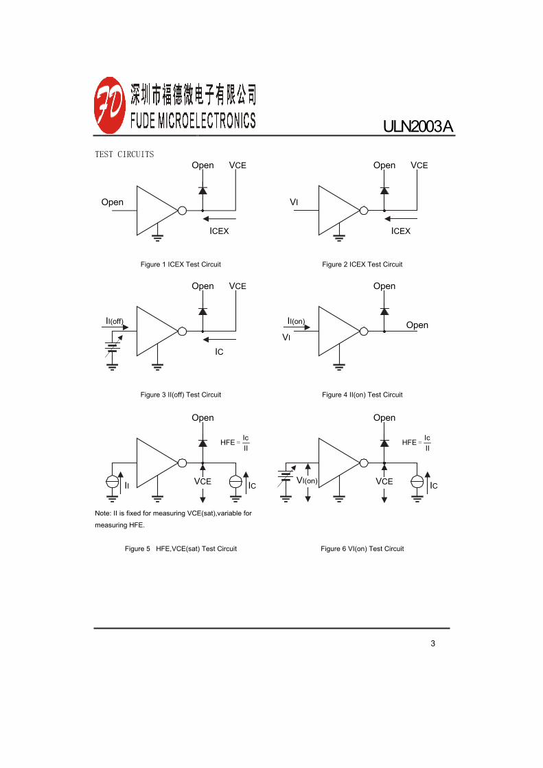
TEST CIRCUITS
ICEX
VCEOpen
Open
ICEX
VCEOpen
VI
tiucriCtseTXECI2erugiFtiucriCtseTXECI1erugiF
IC
VCEOpen
II(off)
Open
II(on) OpenVI
tiucriCtseT)no(II4erugiFtiucriCtseT)ffo(II3erugiF
VCE
Open
IC
IIIcHFE =
II VCE
Open
IC
IIIcHFE =
VI(on)
Note: II is fixed for measuring VCE(sat),variable for
measuring HFE.
tiucriCtseT)no(IV6erugiFtiucriCtseT)tas(ECV,EFH5erugiF
ULN2003A
4
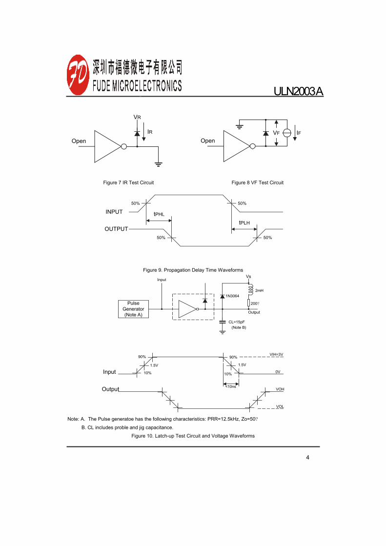
VR
OpenIR IF
OpenVF
tiucriCtseTFV8erugiFtiucriCtseTRI7erugiF
tPHL
tPLH
50%50%
%05%05
INPUT
OUTPUT
Figure 9. Propagation Delay Time Waveforms
PulseGenerator(Note A)
Vs
2mH
200?
1N3064
CL=15pF
Input
Output
(Note B)
1.5V 1.5V
90%
10%
90%
10%
<10ns
Input
Output
VIH=3V
0V
VOH
VOL
Note: A. The Pulse generatoe has the following characteristics: PRR=12.5kHz, Zo=50?
B. CL includes proble and jig capacitance.
Figure 10. Latch-up Test Circuit and Voltage Waveforms
ULN2003A
5
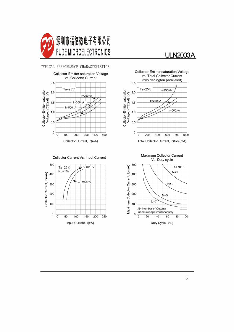
TYPICAL PERFORMANCE CHARACTERISTICS
0 100 200 300 400 5000
0.5
1.0
1.5
2.0
2.5
Collector-Emitter saturation Voltagevs. Collector Current
II=250µA
II=350µA
II=500µA
Collector Current, Ic(mA)
Col
lect
or-E
mitt
ersa
tura
tion
Volta
ge,V
CE(
sat)
(V)
Ta=25
0
0.5
1.0
1.5
2.0
2.5
Col
lect
or-E
mitt
ersa
tura
tion
Volta
ge,V
CE (
sat)
(V)
0 200 400 600 800 1000
Total Collector Current, Ic(tot) (mA)
Collector-Emitter saturation Voltagevs. Total Collector Current(two darlington paralleled)
Ta=25 II=250µA
II=250µA
II=500µA
0 50 100 150 200 250
Input Current, Ii(µA)
0
100
200
300
400
500
Collector Current Vs. Input Current
Ta=25RL=10?
Vs=10V
Vs=8V
Col
lect
orC
urre
nt,I
c(m
A)
0 20 40 60 80 100
Duty Cycle, (%)
0
100
200
300
400
500
Max
imum
Col
lect
orC
urre
nt,I
c(m
A)
Maximum Collector CurrentVs. Duty cycle
N=1
N=2
N=5
N=7
N= Number of OutputsConductiong Simultaneously
Ta=70
ULN2003A
6
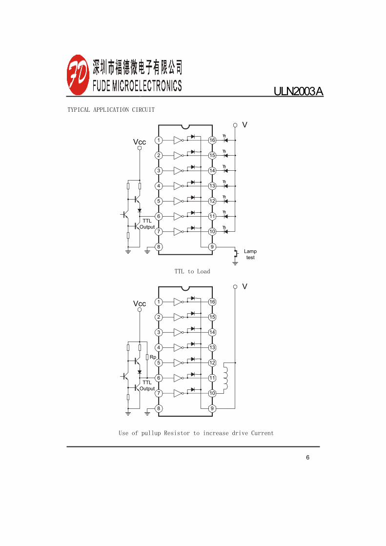
TYPICAL APPLICATION CIRCUIT
1
2
3
4
5
6
7
8
16
15
14
13
12
11
10
9
V
Vcc
TTLOutput
Lamptest
TTL to Load
1
2
3
4
5
6
7
8
16
15
14
13
12
11
10
9
V
Vcc
TTLOutput
Rp
Use of pullup Resistor to increase drive Current


