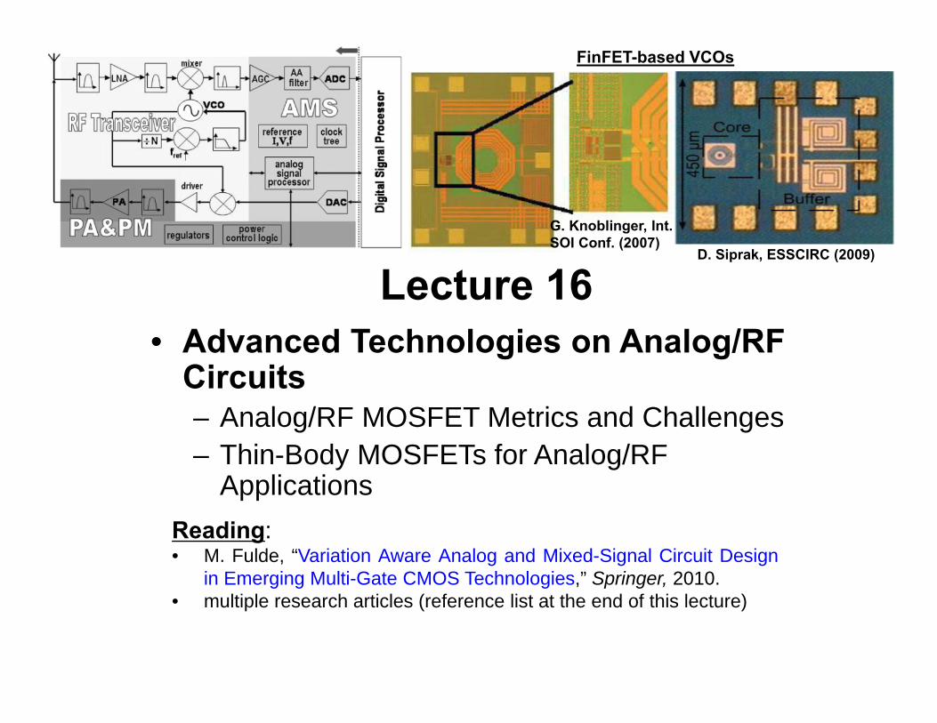
Lecture 16• Advanced Technologies on Analog/RF
Circuits– Analog/RF MOSFET Metrics and Challenges– Thin-Body MOSFETs for Analog/RF
ApplicationsReading:• M. Fulde, “Variation Aware Analog and Mixed-Signal Circuit Design
in Emerging Multi-Gate CMOS Technologies,” Springer, 2010.• multiple research articles (reference list at the end of this lecture)
FinFET-based VCOs
D. Siprak, ESSCIRC (2009)
G. Knoblinger, Int. SOI Conf. (2007)

RF Technology: Not Dictated by Si CMOS!
SiGe Bipolar
RF CMOS
12/2/2013 2Nuo Xu EE 290D, Fall 2013
LF Analog (-0.4 GHz)
RF(-30 GHz)
Millimeter Wave(-300 GHz)
THz
Automotive controls, power management
Cellular (2G-GSM, 3G-CDMA, 4G-LTE)WLAN(Bluetooth, GPS), Serdes, high performance ADC/DAC
60 GHZ point-to-point, radar, wireless backhaul
No product yet
Frequency Range: Applications: Technology:
Source: ITRS (2011)
• For extremely high-frequency and high-power (e.g. PA) applications, SiGe BJT has performance advantage over RF MOSFETs, due to its Larger transconductance (Gm) as well as Gm/Id Higher power density
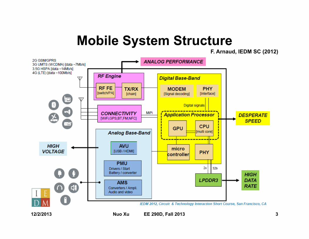
Mobile System StructureF. Arnaud, IEDM SC (2012)
12/2/2013 3Nuo Xu EE 290D, Fall 2013

System on Chip (SoC)65nm SoC (Qualcomm)
DigitalBaseband
RF
• SoC: system integration onto a single IC die higher performance, lower cost
• Preferred to be implemented by LSTP technology, due to: Low power (good for battery-supported mobile devices) Low noise High VDD (easier design for RF/Analog circuits)ä Limited performance (digital clk frequency, fT & fMAX)
A. Cicalini, ISSCC (2011)
12/2/2013 4Nuo Xu EE 290D, Fall 2013
A. Matsuzawa, IEDM (2012)
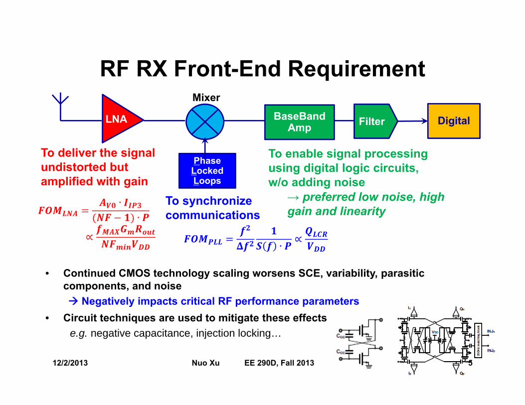
RF RX Front-End Requirement
BaseBandAmp
Phase Locked Loops
FilterLNA
Mixer
To deliver the signal undistorted but amplified with gain
To synchronize communications
To enable signal processing using digital logic circuits, w/o adding noise
• Continued CMOS technology scaling worsens SCE, variability, parasitic components, and noise Negatively impacts critical RF performance parameters
• Circuit techniques are used to mitigate these effectse.g. negative capacitance, injection locking…
Digital
12/2/2013 5Nuo Xu EE 290D, Fall 2013
∙∙
∝∙ ∝
→ preferred low noise, high gain and linearity

Analog-to-Digital Converter (ADC) Requirement
12/2/2013 6Nuo Xu EE 290D, Fall 2013
ADC Type Resolution Speed Power
ConsumptionFlash low ultra-high highSAR low moderate ultra-lowPipeline moderate high lowΣ-∆ high low high
OPA-based:small mismatchhigh gain (>40dB)
Comparator-based:small mismatch
• CMOS scaling larger DIBL lower gain• VDD reduction smaller VGT larger mismatch High-resolution ADCs are extremely challenging!
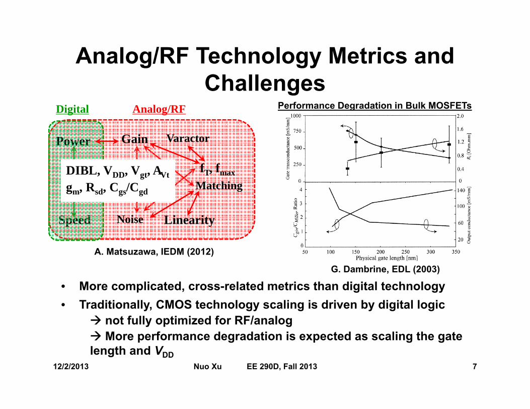
Analog/RF Technology Metrics and Challenges
• More complicated, cross-related metrics than digital technology• Traditionally, CMOS technology scaling is driven by digital logic
not fully optimized for RF/analog More performance degradation is expected as scaling the gate length and VDD
Power
Speed
Gain
Linearity
fT, fmax
Noise
Matching
Varactor
Analog/RFDigital
DIBL, VDD, Vgt, AVtgm, Rsd, Cgs/Cgd
A. Matsuzawa, IEDM (2012)
12/2/2013 7Nuo Xu EE 290D, Fall 2013
G. Dambrine, EDL (2003)
Performance Degradation in Bulk MOSFETs
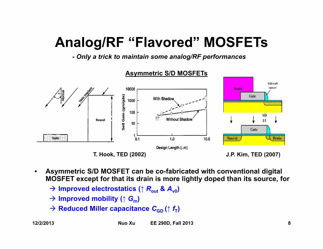
Analog/RF “Flavored” MOSFETs
12/2/2013 8Nuo Xu EE 290D, Fall 2013
Asymmetric S/D MOSFETs
• Asymmetric S/D MOSFET can be co-fabricated with conventional digital MOSFET except for that its drain is more lightly doped than its source, for Improved electrostatics (↑ Rout & Av0) Improved mobility (↑ Gm) Reduced Miller capacitance CGD (↑ fT)
T. Hook, TED (2002) J.P. Kim, TED (2007)
- Only a trick to maintain some analog/RF performances
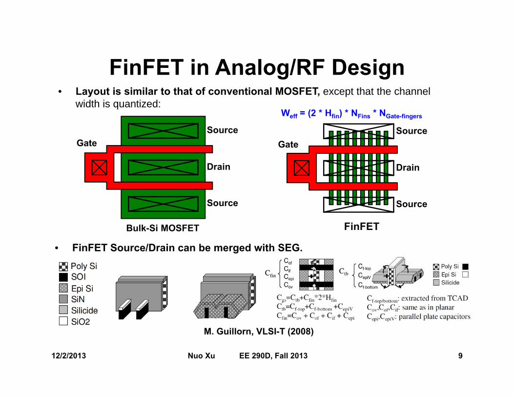
FinFET in Analog/RF Design• Layout is similar to that of conventional MOSFET, except that the channel
width is quantized:
M. Guillorn, VLSI-T (2008)
• FinFET Source/Drain can be merged with SEG.
12/2/2013 9Nuo Xu EE 290D, Fall 2013
Bulk-Si MOSFET
Source
Drain
Source
Gate GateSource
Drain
Source
FinFET
Weff = (2 * Hfin) * NFins * NGate-fingers
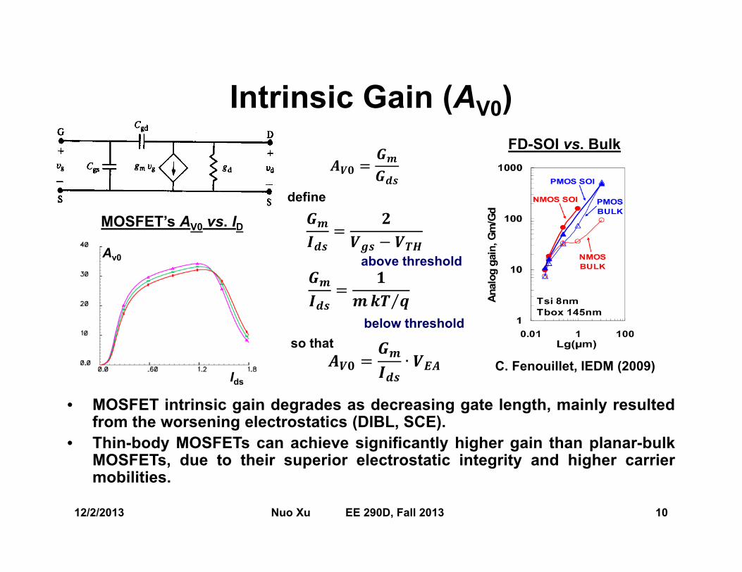
Intrinsic Gain (AV0)
C. Fenouillet, IEDM (2009)
12/2/2013 10Nuo Xu EE 290D, Fall 2013
FD-SOI vs. Bulk
• MOSFET intrinsic gain degrades as decreasing gate length, mainly resultedfrom the worsening electrostatics (DIBL, SCE).
• Thin-body MOSFETs can achieve significantly higher gain than planar-bulkMOSFETs, due to their superior electrostatic integrity and higher carriermobilities.
MOSFET’s AV0 vs. ID
so that
define
Ids
Av0 above threshold
below threshold

FinFET Intrinsic Gain
T. Chiarella, SSE (2010)
12/2/2013 11Nuo Xu EE 290D, Fall 2013
• FinFET shows over 20 dB gain increase over planar MOSFETs.• SOI FinFET (with no well doping) outperforms bulk FinFET (with
retrograde well doping).
Planar vs. FinFET SOI FinFET vs. Bulk FinFET
P. Wambacq, TCS (2007)
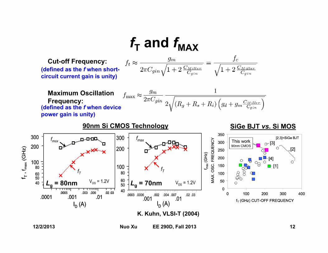
fT and fMAX
12/2/2013 12Nuo Xu EE 290D, Fall 2013
K. Kuhn, VLSI-T (2004)
90nm Si CMOS Technology
Lg = 80nm Lg = 70nm
SiGe BJT vs. Si MOS
Cut-off Frequency:
Maximum Oscillation Frequency:
(defined as the f when short-circuit current gain is unity)
(defined as the f when device power gain is unity)
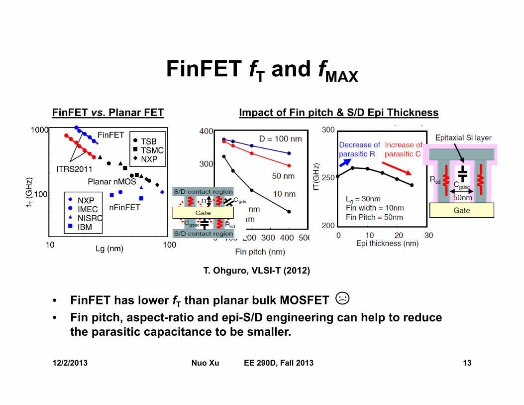
FinFET fT and fMAX
12/2/2013 13Nuo Xu EE 290D, Fall 2013
• FinFET has lower fT than planar bulk MOSFET• Fin pitch, aspect-ratio and epi-S/D engineering can help to reduce
the parasitic capacitance to be smaller.
FinFET vs. Planar FET
. .(
Impact of Fin pitch & S/D Epi Thickness
T. Ohguro, VLSI-T (2012)

Linearity
12/2/2013 14Nuo Xu EE 290D, Fall 2013
• The nonlinear products caused by nth order distortion appearing at n times the frequency of the input (base) tone.
• Related to MOSFET Gm degradation slope.
Planar LSTP Technology
M.-T. Yang, VLSI-T (2011)
where
defineOutput Waveform Distortions

FinFET Linearity
12/2/2013 15Nuo Xu EE 290D, Fall 2013
• FinFET has comparable VIP3 as planar bulk MOSFET.• Sensitivity of VIP3 to device parameter variations can be reduced by
using multiple fin widths (self-cascode) to achieve a broader maximum.
M. Fulde, Springer Series in Adv. Microelec. (2010)V. Subramanian, IEDM (2005)
VIP3 dependence on Fin WidthPlanar Bulk vs. FinFET
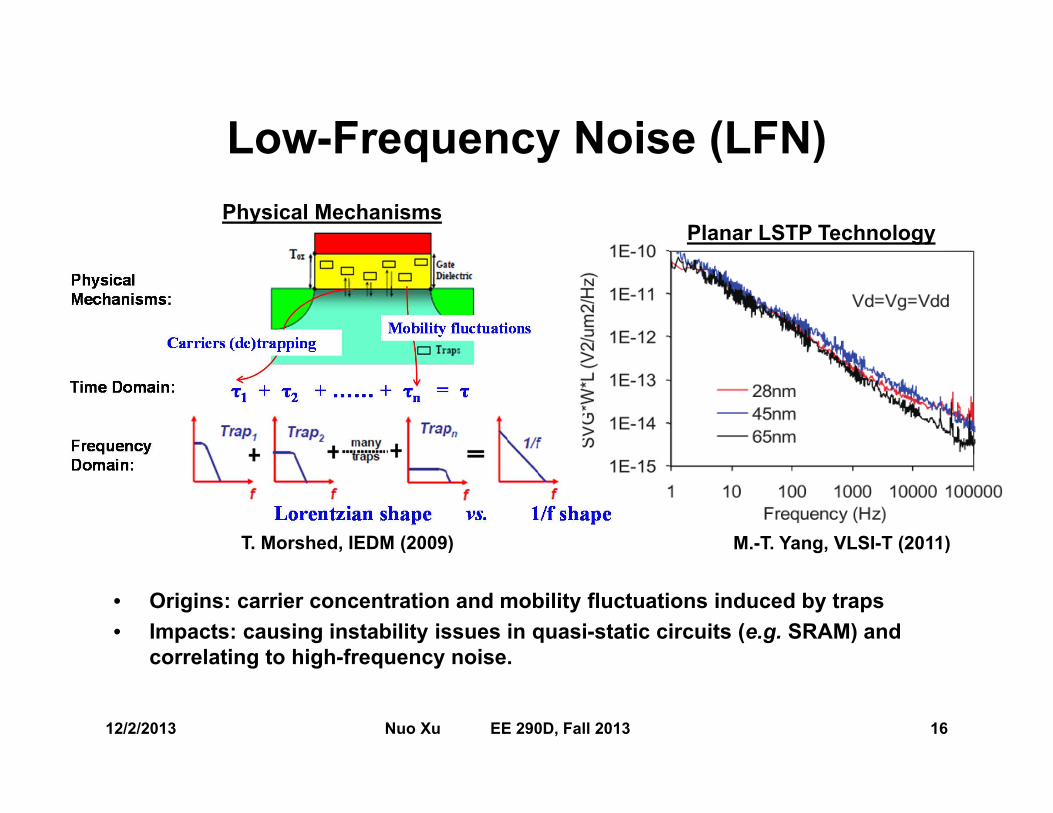
Low-Frequency Noise (LFN)
12/2/2013 16Nuo Xu EE 290D, Fall 2013
Planar LSTP TechnologyPhysical Mechanisms
M.-T. Yang, VLSI-T (2011)
• Origins: carrier concentration and mobility fluctuations induced by traps• Impacts: causing instability issues in quasi-static circuits (e.g. SRAM) and
correlating to high-frequency noise.
T. Morshed, IEDM (2009)
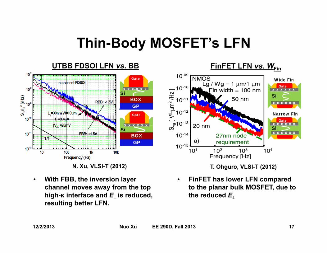
Thin-Body MOSFET’s LFN
12/2/2013 17Nuo Xu EE 290D, Fall 2013
Gate
Six x x x x x
Gatex x x x x xSix x x x x x
x x x x x x
Narrow Fin
Wide Fin
• FinFET has lower LFN compared to the planar bulk MOSFET, due to the reduced E
T. Ohguro, VLSI-T (2012)
FinFET LFN vs. WFinUTBB FDSOI LFN vs. BB
N. Xu, VLSI-T (2012)
• With FBB, the inversion layer channel moves away from the top high-κ interface and E is reduced, resulting better LFN.
BOXGP
Gate
x x x x x x
BOXGP
Gate
x x x x x x
Si
Si

Minimum Noise Figure (NFmin)
• A measure of the degradation of SNR, defined as:
• Minimizing the Miller capacitance is the key to achieve low NFmin in FinFETs.
2 4 6 8 10
0.2
0.4
0.6
0.8
1.0
1.2
1.4
Cmiller
Rgate
NF m
in (d
B)
Scaling Factor
RS/D
All
12/2/2013 18Nuo Xu EE 290D, Fall 2013
28nm LSTP Technology FinFET
M.-T. Yang, VLSI-T (2011) M. Badaroglu, IEDM Tutorial (2012)

MOS Varactors
12/2/2013 19Nuo Xu EE 290D, Fall 2013
• Large RS/D limits the quality factor (Q). Use wide (quasi-planar) fins for VCO
f =5 GHz
Q‐fa
ctor
70nm
5um
P. Wambacq, TED (2007)
28nm LSTP Technology FinFET
M.-T. Yang, VLSI-T (2011)
• Mainly for VCO,PLL applications• Capacitive tuning ratio and
voltage swing are two major metrics
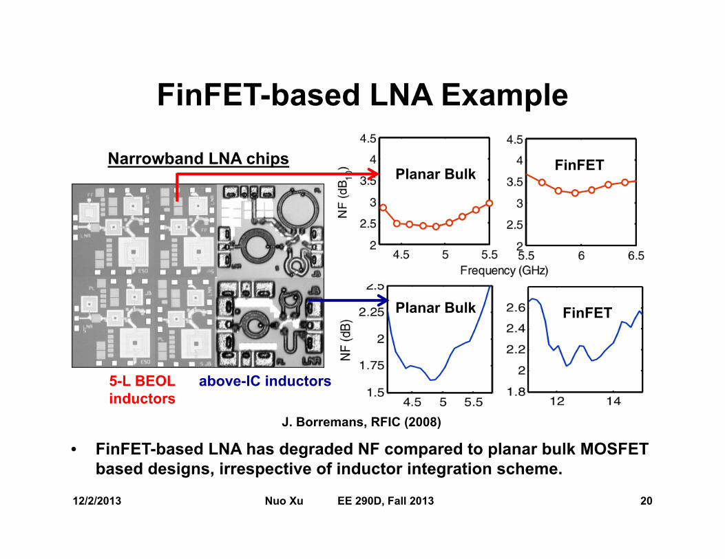
FinFET-based LNA Example
J. Borremans, RFIC (2008)
• FinFET-based LNA has degraded NF compared to planar bulk MOSFET based designs, irrespective of inductor integration scheme.
above-IC inductors5-L BEOL inductors
Planar Bulk
Planar Bulk FinFET
FinFETNarrowband LNA chips
12/2/2013 20Nuo Xu EE 290D, Fall 2013
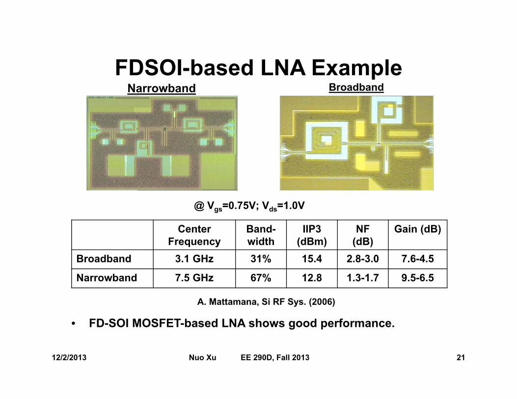
FDSOI-based LNA Example
12/2/2013 21Nuo Xu EE 290D, Fall 2013
BroadbandNarrowband
Center Frequency
Band-width
IIP3(dBm)
NF (dB)
Gain (dB)
Broadband 3.1 GHz 31% 15.4 2.8-3.0 7.6-4.5
Narrowband 7.5 GHz 67% 12.8 1.3-1.7 9.5-6.5
@ Vgs=0.75V; Vds=1.0V
A. Mattamana, Si RF Sys. (2006)
• FD-SOI MOSFET-based LNA shows good performance.
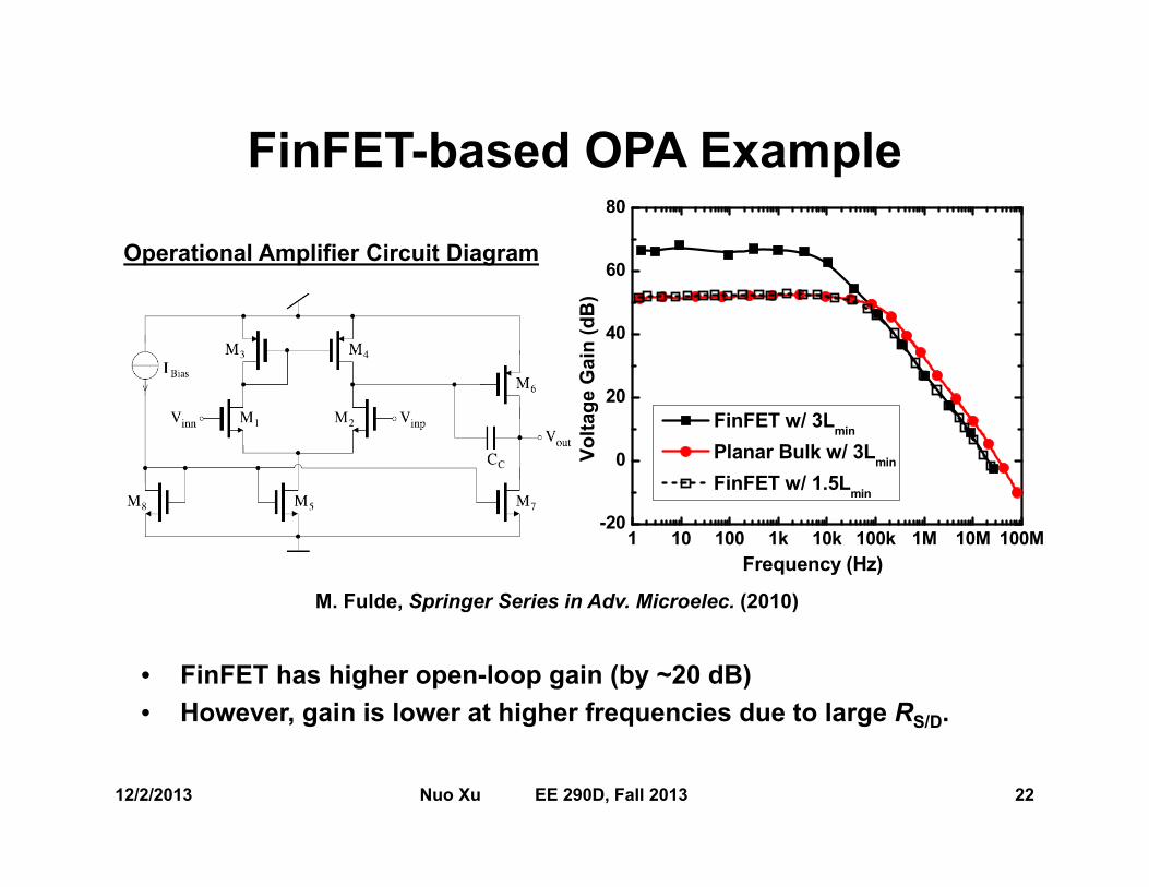
FinFET-based OPA Example
12/2/2013 22Nuo Xu EE 290D, Fall 2013
1 10 100 1k 10k 100k 1M 10M 100M-20
0
20
40
60
80
Volta
ge G
ain
(dB
)Frequency (Hz)
FinFET w/ 3Lmin Planar Bulk w/ 3Lmin
FinFET w/ 1.5Lmin
Operational Amplifier Circuit Diagram
• FinFET has higher open-loop gain (by ~20 dB)• However, gain is lower at higher frequencies due to large RS/D.
M. Fulde, Springer Series in Adv. Microelec. (2010)

References1. A. Cicalini et al., “A 65nm CMOS SoC with embedded HSDPA/EDGE transceiver, digital baseband
and multimedia processor,” ISSCC Digest of Technical Papers, pp. 368-370, 2011.2. A. Matsuzawa, “Analog and RF circuits design and future devices interaction,” IEDM Technical
Digest, pp. 331-334, 2012.3. J.-P. Raskin et al., “Analog/RF performance of multiple gate SOI devices: wideband simulations and
characterization,” IEEE Transactions on Electron Devices, vol. 53, pp. 1088-1095, 2006.4. T. Chiarella et al., “Benchmarking SOI and bulk FinFET alternatives for planar CMOS scaling
succession,” Solid State Electronics, vol. 54, pp. 855-860, 2010.5. P. Wambacq et al., “The potential of FinFETs for analog and RF circuit applications,” IEEE
Transactions on Circuits and Systems, vol. 54, pp. 2541-2551, 2007.6. T. Ohguro et al., “The optimum device parameters for high RF and Analog/MS performance in
planar MOSFET and FinFET,” Symposium on VLSI Technology, pp. 149-150, 2012.7. G. Knoblinger et al., “Evaluation of FinFET RF building blocks,” IEEE International SOI Conference,
pp. 39-40, 2007.8. D. Siprak et al., “FinFET RF receiver building blocks operating above 10 GHz,” Proceedings of the
European Solid-State Circuits Research Conference, 2009.9. J. Borremans et al., “Perspective of RF design in future planar and FinFET CMOS,” Radio
Frequency Integrated Circuits Symposium, pp. 75-78, 2008.10. A. Mattamana et al., “Narrow and broadband low-noise amplifiers at higher frequency using FDSOI
CMOS technology,” Silicon Monolithic Integrated Circuits in RF Systems, Digest of TechnicalPapers, 2006.
11. A. Mattamana et al., “X-band receiver module in fully depleted silicon on insulator technology,”IEEE International SOI Conference, 2012.
12. M. Badaroglu et al., “Scaling challenges of analog electronics,” 2012 IEDM Tutorial, 2012.


