www.longsys.com Longsys Electronics
Rev. 1.3 NCEMASLD-xxG
FORESEE eMMC
NCEMASLD-xxG
Datasheet
Version: 1.3
2018.04.19
LONGSYS ELECTRONICS RESERVES THE RIGHT TO CHANGE PRODUCTS, INFORMATION
AND SPECIFICATIONS WITHOUT NOTICE.
Products and specifications discussed herein are for reference purposes only. All
information discussed herein is provided on an “AS IS” basis, without warranties of any kind.
This document and all information discussed herein remain the sole and exclusive
property of Longsys Electronics. No license of any patent, copyright, mask work, trademark
or any other intellectual property right is granted by one party to the other party under this
document, by implication, estoppel or other-wise.
Longsys products are not intended for use in life support, critical care, medical, safety
equipment, or similar applications where product failure could result in loss of life or personal
or physical harm, or any military or defense application, or any governmental procurement
to which special terms or provisions may apply.
For updates or additional information about Longsys products, contact your nearest
Longsys office.
All brand names, trademarks and registered trademarks belong to their respective
owners.
ⓒ 2018 Shenzhen Longsys Electronics Co., Ltd. All rights reserved.
www.longsys.com Longsys Electronics
Rev. 1.3 NCEMASLD-xxG
Revision History:
Rev. Date Changes Remark
1.0 2018/01/30 Basic spec and architecture Preliminary
1.1 2018/03/29 Revise some descriptions
1.2 2018/04/11 Add NCEMASLD-64G
1.3 2018/04/19 Revise some descriptions
www.longsys.com Longsys Electronics
Rev. 1.3 NCEMASLD-xxG
CONTENTS
1. Introduction .......................................................................................................................... 1
2. Product List ........................................................................................................................... 1
3. Features ................................................................................................................................ 1
4. Functional Description ........................................................................................................... 2
5. Product Specifications ........................................................................................................... 3
5.1 Performance (Typical value) ................................................................................................ 3
5.2 Power Consumption ............................................................................................................ 3
6. Pin Assignments .................................................................................................................... 4
6.1 Ball Array view ................................................................................................................... 4
7. Usage Overview ..................................................................................................................... 6
7.1 General description............................................................................................................. 6
7.2 Partition Management ......................................................................................................... 6
7.3 Automatic Sleep Mode ........................................................................................................ 8
7.4 Sleep (CMD5) .................................................................................................................... 8
7.5 H/W Reset operation........................................................................................................... 9
7.6 High-speed mode selection .................................................................................................. 9
7.7 Bus width selection ............................................................................................................. 9
7.8 Partition configuration ......................................................................................................... 9
7.9 CID register ................................................................................................................... 10
7.10 CSD register .................................................................................................................. 10
7.11 Extended CSD register .................................................................................................... 10
7.12 OCR Register ................................................................................................................. 22
7.13 Field firmware update(FFU) .............................................................................................. 22
7.14 S.M.A.R.T. Health Report ................................................................................................. 24
8. Package Dimension .............................................................................................................. 25
9 Connection Guide .................................................................................................................. 25
9.1 Schematic Diagram .......................................................................................................... 25
10. Processing Guide ............................................................................................................... 26
www.longsys.com Page 1 Longsys Electronics
Rev. 1.3 NCEMASLD-xxG
1. IntroductionFORESEE eMMC is an embedded storage solution designed in the BGA package. The FORESEE eMMC
consists of NAND flash and eMMC controller. The controller could manage the interface protocols,
wear-leveling,bad block management and ECC.
FORESEE eMMC has high performance at a competitive cost, high quality and low power consumption, and
eMMC is compatible with JEDEC standard eMMC 5.1 specifications.
2. Product List
Density Part Number NAND Flash
Type
Capacity
(User Density: 90%)
Package
Size(mm)
Package
Type
32GB NCEMASLD-32G 256Gb x1 28.8GB 11.5x13x1.0 153FBGA
64GB NCEMASLD-64G 256Gb x2 57.6GB 11.5x13x1.0 153FBGA
3. Features eMMC5.1 specification compatibility
(Backward compatible to eMMC4.41/4.5/5.0)
Bus mode
- Data bus width: 1 bit (default), 4 bits, 8 bits
- Data transfer rate: up to 400MB/s (HS400)
- MMC I/F Clock frequency : 0~200MHz
Operating voltage range
- Vcc(NAND) : 2.7 - 3.6V
- Vccq(Controller) : 1.7 - 1.95V / 2.7 - 3.6V
Temperature
- Operation (-25℃ ~ +85℃)
- Storage without operation (-40℃ ~ +85℃)
Sudden-Power-Loss safeguard
Hardware ECC engine
Unique firmware backup mechanism
Global-wear-leveling
Supported features.
- HS400, HS200
- Partitioning, RPMB
- Boot feature, boot partition
- HW Reset/SW Reset
- Discard, Trim, Erase, Sanitize
- Background operations, HPI
- Enhanced reliable write
- S.M.A.R.T. Health Report
- FFU
- Sleep / awake
Others
- Compliance with the RoHS Directive

www.longsys.com Page 2 Longsys Electronics
Rev. 1.3 NCEMASLD-xxG
4. Functional Description FORESEE eMMC with powerful L2P (Logical to Physical) NAND Flash management algorithm provides
unique functions:
Host independence from details of operating NAND flash
Internal ECC to correct defect in NAND flash
Sudden-Power-Loss safeguard
To prevent from data loss, a mechanism named Sudden-Power-Loss safeguard is added in the eMMC.
In the case of sudden power-failure, the eMMC would work properly after power cycling.
Global-wear-leveling
To achieve the best stability and device endurance, this eMMC equips the Global Wear Leveling
algorithm. It ensures that not only normal area, but also the frequently accessed area, such as FAT,
would be programmed and erased evenly.
IDA(Initial Data Acceleration)
The eMMC prevents the pre-burned data from data-loss with IDA, in case of our customer had
pre-burned data to eMMC, before the eMMC being SMT.
Cache
The eMMC enhanced the data written performance with Cache, with which our customer would get
more endurance and reliability.
www.longsys.com Page 3 Longsys Electronics
Rev. 1.3 NCEMASLD-xxG
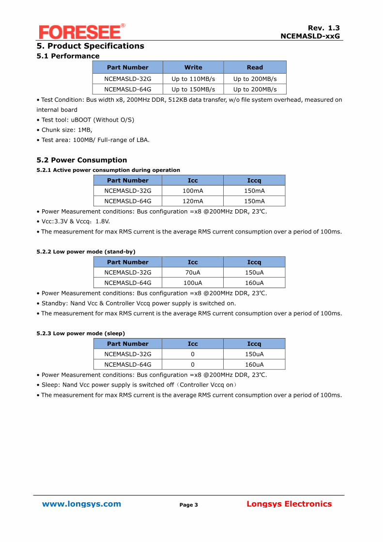
5. Product Specifications
5.1 Performance
Part Number Write Read
NCEMASLD-32G Up to 110MB/s Up to 200MB/s
NCEMASLD-64G Up to 150MB/s Up to 200MB/s
• Test Condition: Bus width x8, 200MHz DDR, 512KB data transfer, w/o file system overhead, measured on
internal board
• Test tool: uBOOT (Without O/S)
• Chunk size: 1MB,
• Test area: 100MB/ Full-range of LBA.
5.2 Power Consumption
5.2.1 Active power consumption during operation
Part Number Icc Iccq
NCEMASLD-32G 100mA 150mA
NCEMASLD-64G 120mA 150mA
• Power Measurement conditions: Bus configuration =x8 @200MHz DDR, 23℃.
• Vcc:3.3V & Vccq:1.8V.
• The measurement for max RMS current is the average RMS current consumption over a period of 100ms.
5.2.2 Low power mode (stand-by)
Part Number Icc Iccq
NCEMASLD-32G 70uA 150uA
NCEMASLD-64G 100uA 160uA
• Power Measurement conditions: Bus configuration =x8 @200MHz DDR, 23℃.
• Standby: Nand Vcc & Controller Vccq power supply is switched on.
• The measurement for max RMS current is the average RMS current consumption over a period of 100ms.
5.2.3 Low power mode (sleep)
Part Number Icc Iccq
NCEMASLD-32G 0 150uA
NCEMASLD-64G 0 160uA
• Power Measurement conditions: Bus configuration =x8 @200MHz DDR, 23℃.
• Sleep: Nand Vcc power supply is switched off(Controller Vccq on)
• The measurement for max RMS current is the average RMS current consumption over a period of 100ms.
www.longsys.com Page 4 Longsys Electronics
Rev. 1.3 NCEMASLD-xxG
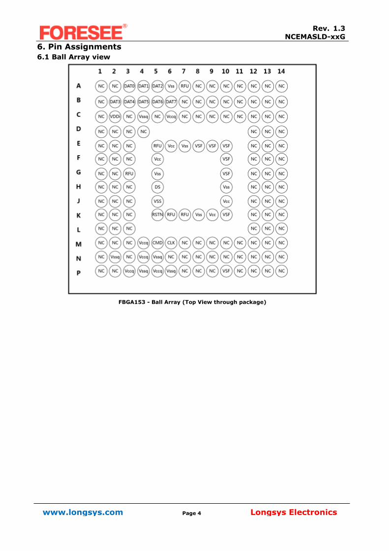
6. Pin Assignments
6.1 Ball Array view
FBGA153 - Ball Array (Top View through package)
www.longsys.com Page 5 Longsys Electronics
Rev. 1.3 NCEMASLD-xxG
6.2 Ball Array view
Signal Description
CLOCK
(CLK)
Each cycle of the clock directs a transfer on the command line and on the data
lines.
COMMAND
(CMD)
This signal is a bidirectional command channel used for device initialization and
command transfer.
The CMD Signal has 2 operation modes: open drain, for initialization, and
push-pull, for command transfer.
Commands are sent from the host to the device, and responses are sent from the
device to the host.
DATA
(DAT0-DAT7)
These are bidirectional data signal. The DAT signals operate in push-pull mode.
By default, after power-up or RESET, only DAT0 is used for data transfer. The
controller can configure a wider data bus for data transfer wither using DAT
[3:0](4bit mode)or DAT[7:0](8bit mode).
Includes internal pull-up resistors for data lines DAT[7:1].Immediately after
entering the 4-bit mode, the device disconnects the internal pull-up resistors on
the DAT1 and DAT2 lines.(The DAT3 line internal pull-up is left connected.)Upon
entering the 8bit mode, the device disconnects the internal pull-up on the DAT1,
DAT2, and DAT[7:4]lines.
Data Strobe
(DS)
Newly assigned pin for HS400 mode. Data Strobe is generated from e.MMC to
host.
In HS400 mode, read data and CRC response are synchronized with Data Strobe.
RESET
(RSTN) Hardware Reset Input
Vccq Vccq is the power supply line for host interface, have two power mode: High power
mode:2.7V~3.6V; Lower power mode:1.7V~1.95V
Vcc Vcc is the power supply line for internal flash memory, its power voltage range
is:2.7V~3.6V
VDDi VDDi is internal power node, not the power supply. Connect 1uF capacitor VDDi to
ground
Vss,Vssq Ground lines.
Note:
NC: No Connect, shall be connected to ground or left floating.
RFU: Reserved for Future Use, must be left floating for future use.
VSF: Vendor Specific Function, must be left floating.
www.longsys.com Page 6 Longsys Electronics
Rev. 1.3 NCEMASLD-xxG
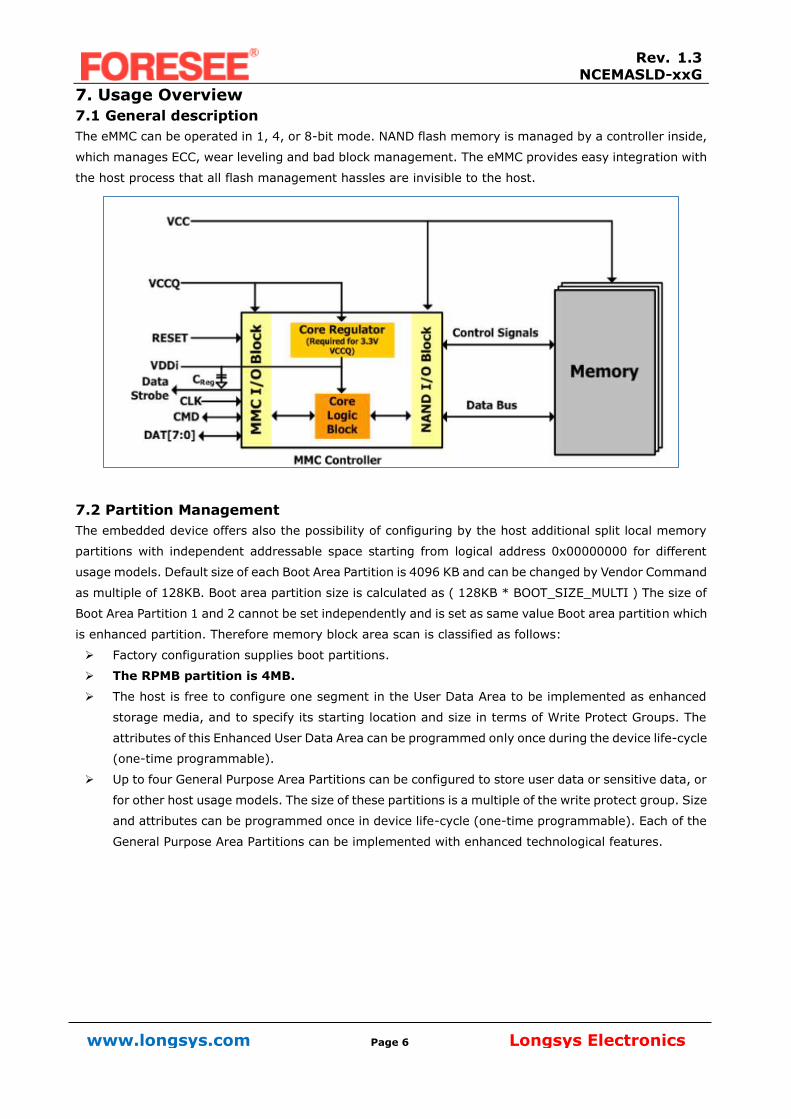
7. Usage Overview
7.1 General description
The eMMC can be operated in 1, 4, or 8-bit mode. NAND flash memory is managed by a controller inside,
which manages ECC, wear leveling and bad block management. The eMMC provides easy integration with
the host process that all flash management hassles are invisible to the host.
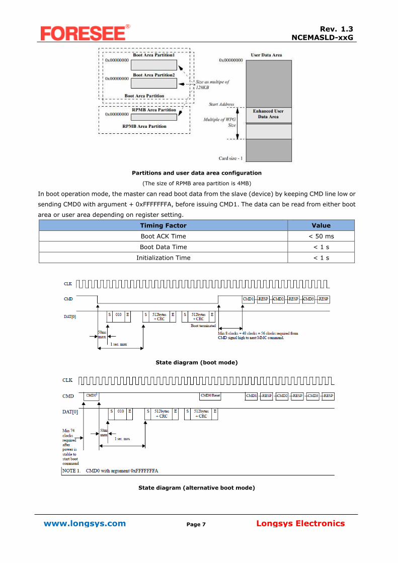
7.2 Partition Management
The embedded device offers also the possibility of configuring by the host additional split local memory
partitions with independent addressable space starting from logical address 0x00000000 for different
usage models. Default size of each Boot Area Partition is 4096 KB and can be changed by Vendor Command
as multiple of 128KB. Boot area partition size is calculated as ( 128KB * BOOT_SIZE_MULTI ) The size of
Boot Area Partition 1 and 2 cannot be set independently and is set as same value Boot area partition which
is enhanced partition. Therefore memory block area scan is classified as follows:
Factory configuration supplies boot partitions.
The RPMB partition is 4MB.
The host is free to configure one segment in the User Data Area to be implemented as enhanced
storage media, and to specify its starting location and size in terms of Write Protect Groups. The
attributes of this Enhanced User Data Area can be programmed only once during the device life-cycle
(one-time programmable).
Up to four General Purpose Area Partitions can be configured to store user data or sensitive data, or
for other host usage models. The size of these partitions is a multiple of the write protect group. Size
and attributes can be programmed once in device life-cycle (one-time programmable). Each of the
General Purpose Area Partitions can be implemented with enhanced technological features.
www.longsys.com Page 7 Longsys Electronics
Rev. 1.3 NCEMASLD-xxG
Partitions and user data area configuration
(The size of RPMB area partition is 4MB)
In boot operation mode, the master can read boot data from the slave (device) by keeping CMD line low or
sending CMD0 with argument + 0xFFFFFFFA, before issuing CMD1. The data can be read from either boot
area or user area depending on register setting.
Timing Factor Value
Boot ACK Time < 50 ms
Boot Data Time < 1 s
Initialization Time < 1 s
State diagram (boot mode)
State diagram (alternative boot mode)
www.longsys.com Page 8 Longsys Electronics
Rev. 1.3 NCEMASLD-xxG
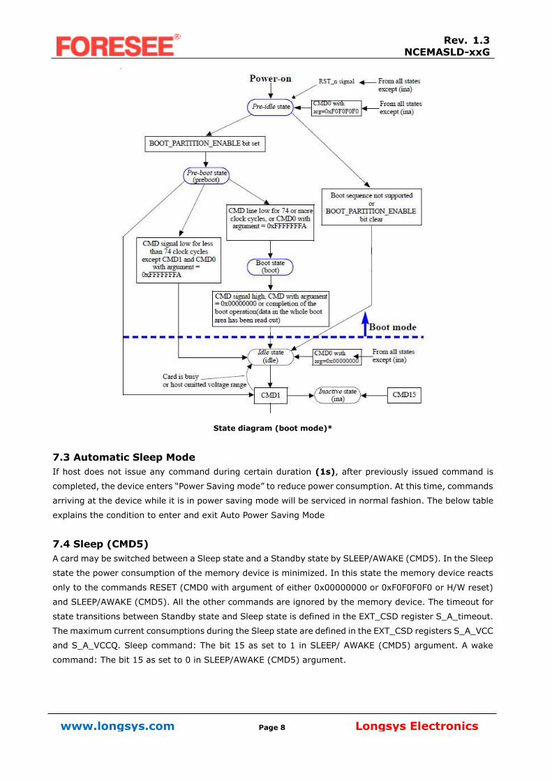
State diagram (boot mode)*
7.3 Automatic Sleep Mode
If host does not issue any command during certain duration (1s), after previously issued command is
completed, the device enters “Power Saving mode” to reduce power consumption. At this time, commands
arriving at the device while it is in power saving mode will be serviced in normal fashion. The below table
explains the condition to enter and exit Auto Power Saving Mode
7.4 Sleep (CMD5)
A card may be switched between a Sleep state and a Standby state by SLEEP/AWAKE (CMD5). In the Sleep
state the power consumption of the memory device is minimized. In this state the memory device reacts
only to the commands RESET (CMD0 with argument of either 0x00000000 or 0xF0F0F0F0 or H/W reset)
and SLEEP/AWAKE (CMD5). All the other commands are ignored by the memory device. The timeout for
state transitions between Standby state and Sleep state is defined in the EXT_CSD register S_A_timeout.
The maximum current consumptions during the Sleep state are defined in the EXT_CSD registers S_A_VCC
and S_A_VCCQ. Sleep command: The bit 15 as set to 1 in SLEEP/ AWAKE (CMD5) argument. A wake
command: The bit 15 as set to 0 in SLEEP/AWAKE (CMD5) argument.
www.longsys.com Page 9 Longsys Electronics
Rev. 1.3 NCEMASLD-xxG
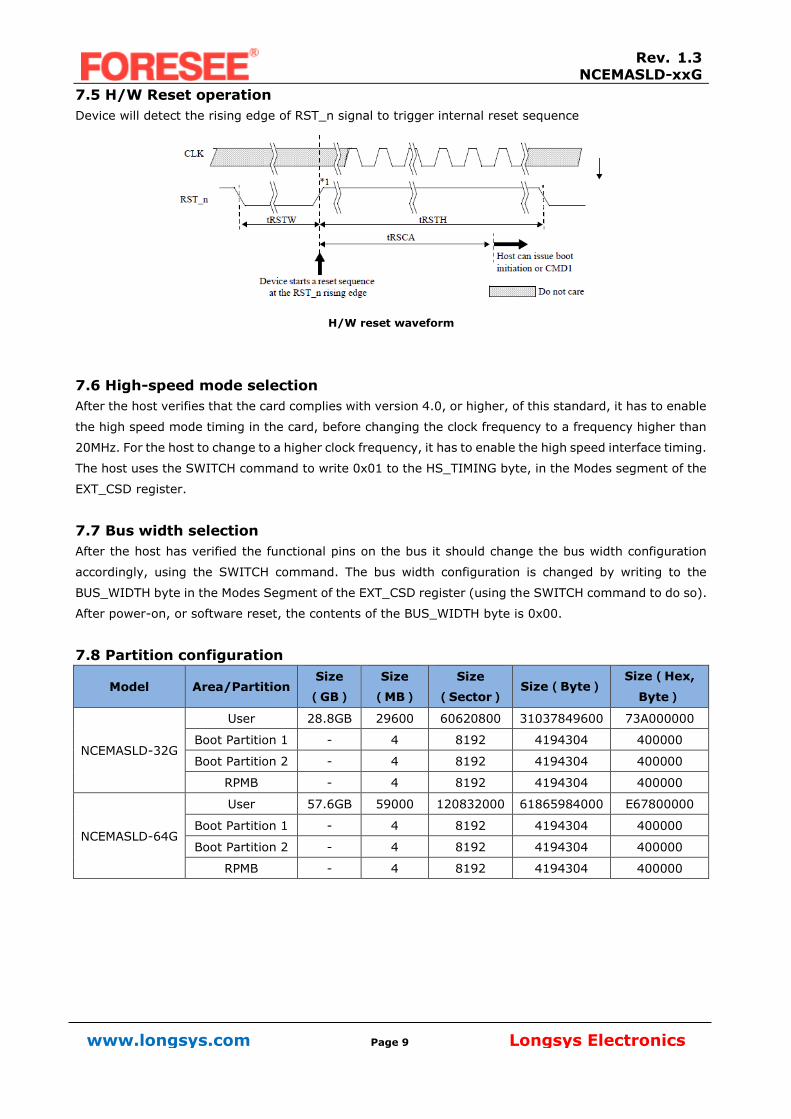
7.5 H/W Reset operation
Device will detect the rising edge of RST_n signal to trigger internal reset sequence
H/W reset waveform
7.6 High-speed mode selection
After the host verifies that the card complies with version 4.0, or higher, of this standard, it has to enable
the high speed mode timing in the card, before changing the clock frequency to a frequency higher than
20MHz. For the host to change to a higher clock frequency, it has to enable the high speed interface timing.
The host uses the SWITCH command to write 0x01 to the HS_TIMING byte, in the Modes segment of the
EXT_CSD register.
7.7 Bus width selection
After the host has verified the functional pins on the bus it should change the bus width configuration
accordingly, using the SWITCH command. The bus width configuration is changed by writing to the
BUS_WIDTH byte in the Modes Segment of the EXT_CSD register (using the SWITCH command to do so).
After power-on, or software reset, the contents of the BUS_WIDTH byte is 0x00.
7.8 Partition configuration
Model Area/Partition Size
(GB)
Size
(MB)
Size
(Sector) Size(Byte)
Size(Hex,
Byte)
NCEMASLD-32G
User 28.8GB 29600 60620800 31037849600 73A000000
Boot Partition 1 - 4 8192 4194304 400000
Boot Partition 2 - 4 8192 4194304 400000
RPMB - 4 8192 4194304 400000
NCEMASLD-64G
User 57.6GB 59000 120832000 61865984000 E67800000
Boot Partition 1 - 4 8192 4194304 400000
Boot Partition 2 - 4 8192 4194304 400000
RPMB - 4 8192 4194304 400000
www.longsys.com Page 10 Longsys Electronics
Rev. 1.3 NCEMASLD-xxG
7.9 CID register
The Card Identification (CID) register is 128 bits wide. It contains the card identification information used
during the card identification phase (protocol). Every individual flash or I/O card shall have an unique
identification number. Every type of ROM cards (defined by content) shall have a unique identification
number. The structure of the CID register is defined in the following sections.
Name Field Width CID-slice CID Value Remark
Manufacturer ID MID 8 [127:120] 88h
Reserved - 6 [119:114] --
Card/BGA CBX 2 [113:112] 01h BGA
OEM/Application ID OID 8 [111:104] 03h
Product name PNM 48 [103:56] 0x534C44333247 SLD32G
0x534C44363447 SLD64G
Product revision PRV 8 [55:48] --
Product serial number PSN 32 [47:16] -- Not Fixed
Manufacturing date MDT 8 [15:8] -- Not Fixed
CRC7 checksum CRC 7 [7:1] -- Not Fixed
Not used, always ‘1’ - 1 [0:0] --
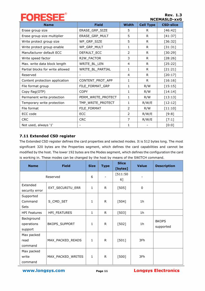
7.10 CSD register
The Card-Specific Data (CSD) register provides information on how to access the card contents. The CSD
defines the data format, error correction type, maximum data access time, data transfer speed, whether
the DSR register can be used etc. The programmable part of the register (entries marked by W or E, see
below) can be changed by CMD27. The type of the CSD Registry entries coded as follows:
Name Field Width Cell Type CSD-slice
CSD structure CSD_STRUCTURE 2 R [127:126]
System specification version SPEC_VERS 4 R [125:122]
Reserved - 2 R [121:120]
Data read access-time 1 TAAC 8 R [119:112]
Data read access-time 2 in CLK
cycles (NSAC*100) NSAC 8 R [111:104]
Max. bus clock frequency TRAN_SPEED 8 R [103:96]
Card command classes CCC 12 R [95:84]
Max. read data block length READ_BL_LEN 4 R [83:80]
Partial blocks for read allowed READ_BL_PARTIAL 1 R [79:79]
Write block misalignment WRITE_BLK_MISALIGN 1 R [78:78]
Read block misalignment READ_BLK_MISALIGN 1 R [77:77]
DSR implemented DSR_IMP 1 R [76:76]
Reserved - 2 R [75:74]
Device size C_SIZE 12 R [73:62]
Max. read current @DDV min VDD_R_CURR_MIN 3 R [61:59]
Max. read current @DDV max VDD_R_CURR_MAX 3 R [58:56]
Max. write current @DDV min VDD_W_CURR_MIN 3 R [55:53]
Max. write current @DDV max VDD_W_CURR_MAX 3 R [52:50]
Device size multiplier C_SIZE_MULT 3 R [49:47]
www.longsys.com Page 11 Longsys Electronics
Rev. 1.3 NCEMASLD-xxG
Name Field Width Cell Type CSD-slice
Erase group size ERASE_GRP_SIZE 5 R [46:42]
Erase group size multiplier ERASE_GRP_MULT 5 R [41:37]
Write protect group size WP_GRP_SIZE 5 R [36:32]
Write protect group enable WP_GRP_MULT 1 R [31:31]
Manufacturer default ECC DEFAULT_ECC 2 R [30:29]
Write speed factor R2W_FACTOR 3 R [28:26]
Max. write data block length WRITE_BL_LEN 4 R [25:22]
Partial blocks for write allowed WRITE_BL_PARTIAL 1 R [21:21]
Reserved - 4 R [20:17]
Content protection application CONTENT_PROT_APP 1 R [16:16]
File format group FILE_FORMAT_GRP 1 R/W [15:15]
Copy flag(OTP) COPY 1 R/W [14:14]
Permanent write protection PERM_WRITE_PROTECT 1 R/W [13:13]
Temporary write protection TMP_WRITE_PROTECT 1 R/W/E [12:12]
File format FILE_FORMAT 2 R/W [11:10]
ECC code ECC 2 R/W/E [9:8]
CRC CRC 7 R/W/E [7:1]
Not used, always ‘1‘ - 1 - [0:0]
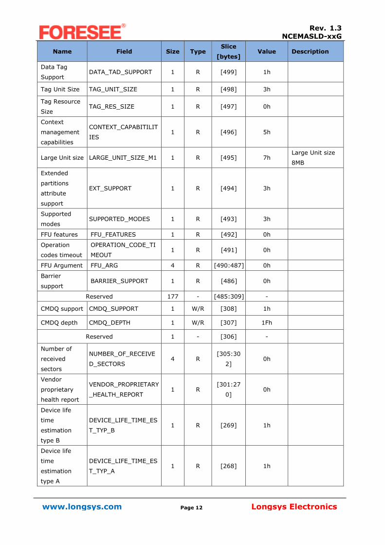
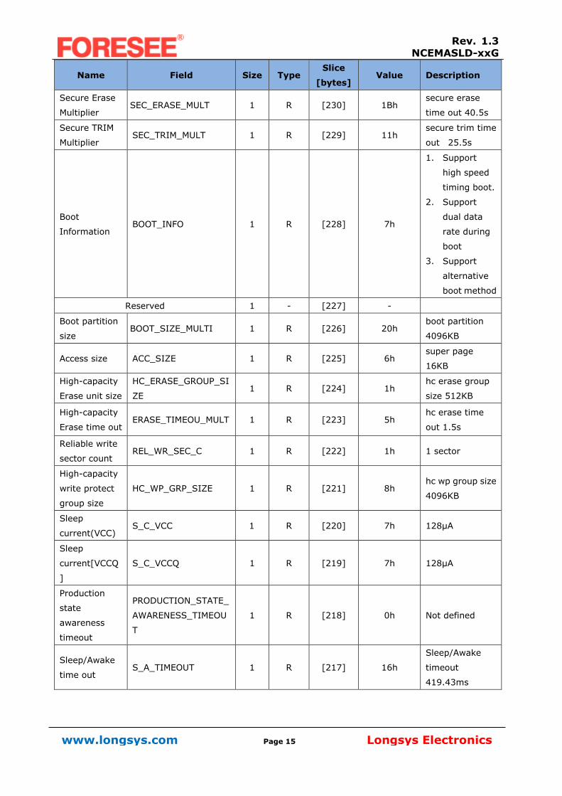
7.11 Extended CSD register
The Extended CSD register defines the card properties and selected modes. It is 512 bytes long. The most
significant 320 bytes are the Properties segment, which defines the card capabilities and cannot be
modified by the host. The lower 192 bytes are the Modes segment, which defines the configuration the card
is working in. These modes can be changed by the host by means of the SWITCH command.
Name Field Size Type Slice
[bytes] Value Description
Reserved 6 - [511:50
6] -
Extended
security error EXT_SECURITU_ERR 1 R [505] 0
Supported
Command
Sets
S_CMD_SET 1 R [504] 1h
HPI Features HPI_FEATURES 1 R [503] 1h
Background
operations
support
BKOPS_SUPPORT 1 R [502] 1h BKOPS
supported
Max packed
read
command
MAX_PACKED_READS 1 R [501] 3Fh
Max packed
write
command
MAX_PACKED_WRITES 1 R [500] 3Fh
www.longsys.com Page 12 Longsys Electronics
Rev. 1.3 NCEMASLD-xxG
Name Field Size Type Slice
[bytes] Value Description
Data Tag
Support DATA_TAD_SUPPORT 1 R [499] 1h
Tag Unit Size TAG_UNIT_SIZE 1 R [498] 3h
Tag Resource
Size TAG_RES_SIZE 1 R [497] 0h
Context
management
capabilities
CONTEXT_CAPABITILIT
IES 1 R [496] 5h
Large Unit size LARGE_UNIT_SIZE_M1 1 R [495] 7h Large Unit size
8MB
Extended
partitions
attribute
support
EXT_SUPPORT 1 R [494] 3h
Supported
modes SUPPORTED_MODES 1 R [493] 3h
FFU features FFU_FEATURES 1 R [492] 0h
Operation
codes timeout
OPERATION_CODE_TI
MEOUT 1 R [491] 0h
FFU Argument FFU_ARG 4 R [490:487] 0h
Barrier
support BARRIER_SUPPORT 1 R [486] 0h
Reserved 177 - [485:309] -
CMDQ support CMDQ_SUPPORT 1 W/R [308] 1h
CMDQ depth CMDQ_DEPTH 1 W/R [307] 1Fh
Reserved 1 - [306] -
Number of
received
sectors
NUMBER_OF_RECEIVE
D_SECTORS 4 R
[305:30
2] 0h
Vendor
proprietary
health report
VENDOR_PROPRIETARY
_HEALTH_REPORT 1 R
[301:27
0] 0h
Device life
time
estimation
type B
DEVICE_LIFE_TIME_ES
T_TYP_B 1 R [269] 1h
Device life
time
estimation
type A
DEVICE_LIFE_TIME_ES
T_TYP_A 1 R [268] 1h
www.longsys.com Page 13 Longsys Electronics
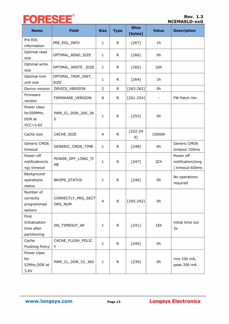
Rev. 1.3 NCEMASLD-xxG
Name Field Size Type Slice
[bytes] Value Description
Pre EOL
information PRE_EOL_INFO 1 R [267] 1h
Optimal read
size OPTIMAL_READ_SIZE 1 R [266] 0h
Optimal write
size OPTIMAL_WRITE _SIZE 1 R [265] 20h
Optimal trim
unit size
OPTIMAL_TRIM_UNIT_
SIZE 1 R [264] 1h
Device version DEVICE_VERSION 2 R [263:262] 0h
Firmware
version FIRMWARE_VERSION 8 R [261:254] - FW Patch Ver.
Power class
for200MHz,
DDR at
VCC=3.6V
PWR_CL_DDR_200_36
0 1 R [253] 0h
Cache size CACHE_SIZE 4 R [252:24
9] 10000h
Generic CMD6
timeout GENERIC_CMD6_TIME 1 R [248] Ah
Generic CMD6
timeout 100ms
Power-off
notification(lo
ng) timeout
POWER_OFF_LONG_TI
ME 1 R [247] 3Ch
Power off
notification(long
) timeout 600ms
Background
operations
status
BKOPS_STATUS 1 R [246] 0h No operations
required
Number of
correctly
programmed
sectors
CORRECTLY_PRG_SECT
ORS_NUM 4 R [245:242] 0h
First
Initialization
time after
partitioning
INI_TIMEOUT_AP 1 R [241] 1Eh initial time out
3s
Cache
Flushing Policy
CACHE_FLUSH_POLIC
Y 1 R [240] 0h
Power class
for
52Mhz,DDR at
3.6V
PWR_CL_DDR_52_360 1 R [239] 0h rms 100 mA,
peak 200 mA
www.longsys.com Page 14 Longsys Electronics
Rev. 1.3 NCEMASLD-xxG
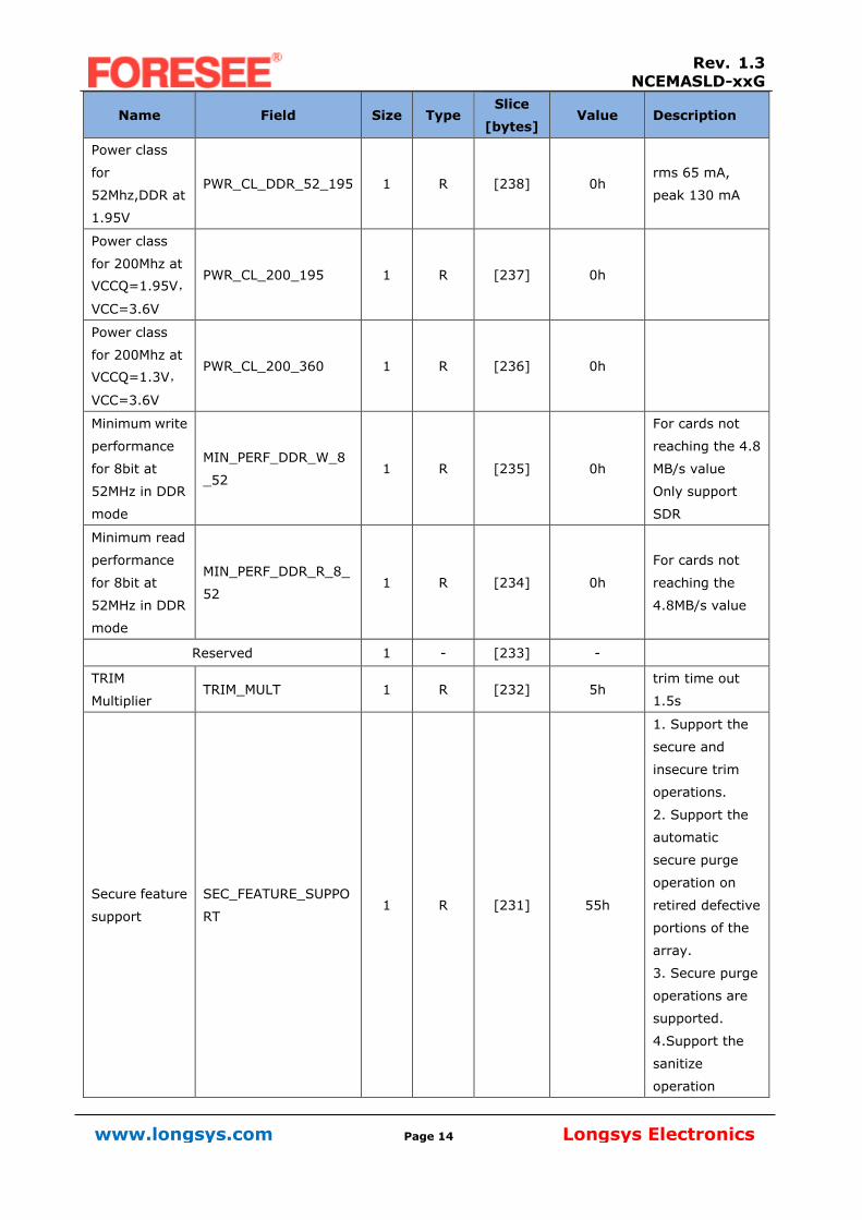
Name Field Size Type Slice
[bytes] Value Description
Power class
for
52Mhz,DDR at
1.95V
PWR_CL_DDR_52_195 1 R [238] 0h rms 65 mA,
peak 130 mA
Power class
for 200Mhz at
VCCQ=1.95V,
VCC=3.6V
PWR_CL_200_195 1 R [237] 0h
Power class
for 200Mhz at
VCCQ=1.3V,
VCC=3.6V
PWR_CL_200_360 1 R [236] 0h
Minimum write
performance
for 8bit at
52MHz in DDR
mode
MIN_PERF_DDR_W_8
_52 1 R [235] 0h
For cards not
reaching the 4.8
MB/s value
Only support
SDR
Minimum read
performance
for 8bit at
52MHz in DDR
mode
MIN_PERF_DDR_R_8_
52 1 R [234] 0h
For cards not
reaching the
4.8MB/s value
Reserved 1 - [233] -
TRIM
Multiplier TRIM_MULT 1 R [232] 5h
trim time out
1.5s
Secure feature
support
SEC_FEATURE_SUPPO
RT 1 R [231] 55h
1. Support the
secure and
insecure trim
operations.
2. Support the
automatic
secure purge
operation on
retired defective
portions of the
array.
3. Secure purge
operations are
supported.
4.Support the
sanitize
operation
www.longsys.com Page 15 Longsys Electronics
Rev. 1.3 NCEMASLD-xxG
Name Field Size Type Slice
[bytes] Value Description
Secure Erase
Multiplier SEC_ERASE_MULT 1 R [230] 1Bh
secure erase
time out 40.5s
Secure TRIM
Multiplier SEC_TRIM_MULT 1 R [229] 11h
secure trim time
out 25.5s
Boot
Information BOOT_INFO 1 R [228] 7h
1. Support
high speed
timing boot.
2. Support
dual data
rate during
boot
3. Support
alternative
boot method
Reserved 1 - [227] -
Boot partition
size BOOT_SIZE_MULTI 1 R [226] 20h
boot partition
4096KB
Access size ACC_SIZE 1 R [225] 6h super page
16KB
High-capacity
Erase unit size
HC_ERASE_GROUP_SI
ZE 1 R [224] 1h
hc erase group
size 512KB
High-capacity
Erase time out ERASE_TIMEOU_MULT 1 R [223] 5h
hc erase time
out 1.5s
Reliable write
sector count REL_WR_SEC_C 1 R [222] 1h 1 sector
High-capacity
write protect
group size
HC_WP_GRP_SIZE 1 R [221] 8h hc wp group size
4096KB
Sleep
current(VCC) S_C_VCC 1 R [220] 7h 128μA
Sleep
current[VCCQ
]
S_C_VCCQ 1 R [219] 7h 128μA
Production
state
awareness
timeout
PRODUCTION_STATE_
AWARENESS_TIMEOU
T
1 R [218] 0h Not defined
Sleep/Awake
time out S_A_TIMEOUT 1 R [217] 16h
Sleep/Awake
timeout
419.43ms
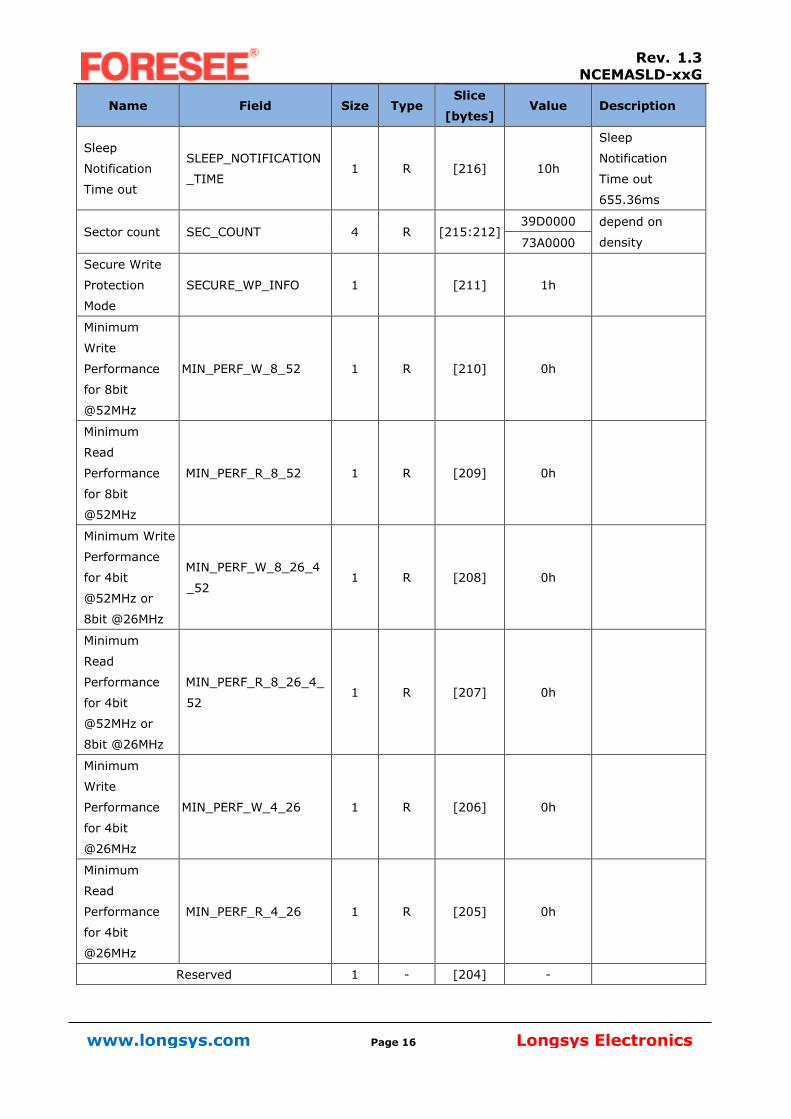
www.longsys.com Page 16 Longsys Electronics
Rev. 1.3 NCEMASLD-xxG
Name Field Size Type Slice
[bytes] Value Description
Sleep
Notification
Time out
SLEEP_NOTIFICATION
_TIME 1 R [216] 10h
Sleep
Notification
Time out
655.36ms
Sector count SEC_COUNT 4 R [215:212] 39D0000 depend on
density 73A0000
Secure Write
Protection
Mode
SECURE_WP_INFO 1 [211] 1h
Minimum
Write
Performance
for 8bit
@52MHz
MIN_PERF_W_8_52 1 R [210] 0h
Minimum
Read
Performance
for 8bit
@52MHz
MIN_PERF_R_8_52 1 R [209] 0h
Minimum Write
Performance
for 4bit
@52MHz or
8bit @26MHz
MIN_PERF_W_8_26_4
_52 1 R [208] 0h
Minimum
Read
Performance
for 4bit
@52MHz or
8bit @26MHz
MIN_PERF_R_8_26_4_
52 1 R [207] 0h
Minimum
Write
Performance
for 4bit
@26MHz
MIN_PERF_W_4_26 1 R [206] 0h
Minimum
Read
Performance
for 4bit
@26MHz
MIN_PERF_R_4_26 1 R [205] 0h
Reserved 1 - [204] -
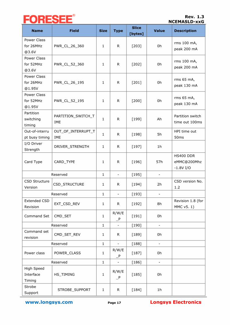
www.longsys.com Page 17 Longsys Electronics
Rev. 1.3 NCEMASLD-xxG
Name Field Size Type Slice
[bytes] Value Description
Power Class
for 26MHz
@3.6V
PWR_CL_26_360 1 R [203] 0h rms 100 mA,
peak 200 mA
Power Class
for 52MHz
@3.6V
PWR_CL_52_360 1 R [202] 0h rms 100 mA,
peak 200 mA
Power Class
for 26MHz
@1.95V
PWR_CL_26_195 1 R [201] 0h rms 65 mA,
peak 130 mA
Power Class
for 52MHz
@1.95V
PWR_CL_52_195 1 R [200] 0h rms 65 mA,
peak 130 mA
Partition
switching
timing
PARTITION_SWITCH_T
IME 1 R [199] Ah
Partition switch
time out 100ms
Out-of-interru
pt busy timing
OUT_OF_INTERRUPT_T
IME 1 R [198] 5h
HPI time out
50ms
I/O Driver
Strength DRIVER_STRENGTH 1 R [197] 1h
Card Type CARD_TYPE 1 R [196] 57h
HS400 DDR
eMMC@200Mhz
-1.8V I/O
Reserved 1 - [195] -
CSD Structure
Version CSD_STRUCTURE 1 R [194] 2h
CSD version No.
1.2
Reserved 1 - [193] -
Extended CSD
Revision EXT_CSD_REV 1 R [192] 8h
Revision 1.8 (for
MMC v5. 1)
Command Set CMD_SET 1 R/W/E
_P [191] 0h
Reserved 1 - [190] -
Command set
revision CMD_SET_REV 1 R [189] 0h
Reserved 1 - [188] -
Power class POWER_CLASS 1 R/W/E
_P [187] 0h
Reserved 1 - [186] -
High Speed
Interface
Timing
HS_TIMING 1 R/W/E
_P [185] 0h
Strobe
Support STROBE_SUPPORT 1 R [184] 1h
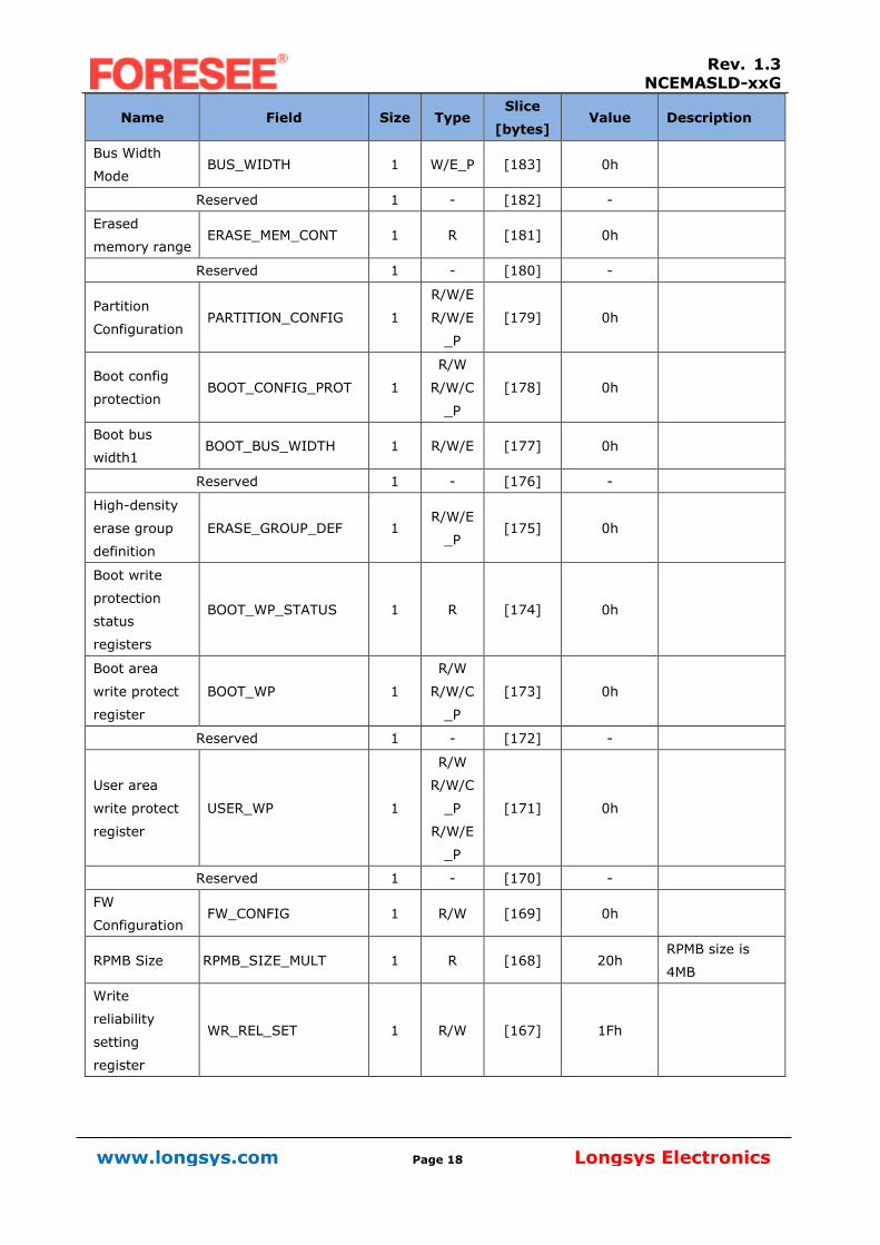
www.longsys.com Page 18 Longsys Electronics
Rev. 1.3 NCEMASLD-xxG
Name Field Size Type Slice
[bytes] Value Description
Bus Width
Mode BUS_WIDTH 1 W/E_P [183] 0h
Reserved 1 - [182] -
Erased
memory range ERASE_MEM_CONT 1 R [181] 0h
Reserved 1 - [180] -
Partition
Configuration PARTITION_CONFIG 1
R/W/E
R/W/E
_P
[179] 0h
Boot config
protection BOOT_CONFIG_PROT 1
R/W
R/W/C
_P
[178] 0h
Boot bus
width1 BOOT_BUS_WIDTH 1 R/W/E [177] 0h
Reserved 1 - [176] -
High-density
erase group
definition
ERASE_GROUP_DEF 1 R/W/E
_P [175] 0h
Boot write
protection
status
registers
BOOT_WP_STATUS 1 R [174] 0h
Boot area
write protect
register
BOOT_WP 1
R/W
R/W/C
_P
[173] 0h
Reserved 1 - [172] -
User area
write protect
register
USER_WP 1
R/W
R/W/C
_P
R/W/E
_P
[171] 0h
Reserved 1 - [170] -
FW
Configuration FW_CONFIG 1 R/W [169] 0h
RPMB Size RPMB_SIZE_MULT 1 R [168] 20h RPMB size is
4MB
Write
reliability
setting
register
WR_REL_SET 1 R/W [167] 1Fh
www.longsys.com Page 19 Longsys Electronics
Rev. 1.3 NCEMASLD-xxG
Name Field Size Type Slice
[bytes] Value Description
Write
reliability
parameter
register
WR_REL_PARAM 1 R [166] 15h
Support the
enhanced
definition of
reliable write
Start Sanitize
operation SANITIZE_START 1 W/E_P [165] 0h
Manually start
background
operations
BKOPS_START 1 W/E_P [164] 0h
Enable
background
operations
handshake
BKOPS_EN 1 R/W [163] 0h
H/W reset
function RST_n_FUNCTION 1 R/W [162] 0h
HPI
management HPI_MGMT 1
R/W/E
_P [161] 0h
Partitioning
support
PARTITIONING_SUPP
ORT 1 R [160] 7h
1. Enhanced
technological
features in
partitions and
user data area.
2. Device
supports
partitioning
features
3. Device can
have extended
partition
attribute
Max Enhanced
Area Size MAX_ENH_SIZE_MULT 3 R
[159:15
7] 9A2h
Partitions
attribute
PARTITIONS_ATTRIBU
TE 1 R/W [156] 0h
Partitions
setting
PARTITIONS_SETTING
_COMPLETED 1 R/W [155] 0h
General
Purpose
Partition Size
GP_SIZE_MULT 12 R/W [154:14
3] 0h
Enhanced
User Data
Area Size
ENH_SIZE_MULT 3 R/W [142:14
0] 0h
www.longsys.com Page 20 Longsys Electronics
Rev. 1.3 NCEMASLD-xxG
Name Field Size Type Slice
[bytes] Value Description
Enhanced
User Data
Start Address
ENH_START_ADDR 4 R/W [139:13
6] 0h
Reserved 1 - [135] -
Secure Bad
Block
Management
Mode
SEC_BAD_BLK_MGMN
T 1 R/W [134] 0h
Production
state
awareness
PRODUCTION_STATE_
AWARENESS 1 R/W/E [133] 0h
Package Case
Temperature
is controlled
TCASE_SUPPORT 1 W/E_P [132] 0h
Periodic
Wake-up PERIODIC_WAKEUP 1 R/W/E [131] 0h
Program
CID/CSD in
DDR mode
support
PROGRAM_CID_CSD_
DDR_SUPPORT 1 R [130] 1h
Reserved 2 - [129:12
8] -
Vendor
specific field
VENDOR_SPECIFIC_FI
ELD 64
<vend
or
specfic
>
[127:64] 0h
Native sector
size
NATIVE_SECTOR_SIZ
E 1 R [63] 0h
Sector size
emulation USE_NATIVE_SECTOR 1 R/W [62] 0h
Sector size DATA_SECTOR_SIZE 1 R [61] 0h
1st
initialization
after disabling
sector size
emulation
INI_TIMEOUT_EMU 1 R [60] 0h
Class 6
commands
control
CLASS_6_CTRL 1 R/W/E
_P [59] 0h
www.longsys.com Page 21 Longsys Electronics
Rev. 1.3 NCEMASLD-xxG
Name Field Size Type Slice
[bytes] Value Description
Number of
addressed
group to be
Released
DYNCAP_NEEDED 1 R [58] 0h
Exception
events control
EXCEPTION_EVENTS_
CTRL 2
R/W/E
_P [57:56] 0h
Exception
events status
EXCEPTION_EVENTS_
STATUS 2 R [55:54] 0h
Extended
Partitions
Attribute
EXT_PARTITIONS_ATT
RIBUTE 2 R/W [53:52] 0h
Context
configuration CONTEXT_CONF 15
R/W/E
_P [51:37] 0h
Packed
command
status
PACKED_COMMAND_S
TATUS 1 R [36] 0h
Packed
command
failure index
PACKED_FAILURE_IN
DEX 1 R [35] 0h
Power Off
Notification
POWER_OFF_NOTIFIC
ATION 1
R/W/E
_P [34] 0h
Control to turn
the Cache
ON/OFF
ON/OFF CACHE_CTRL 1 R/W/E
_P [33] 0h
Flushing of the
cache FLUSH_CACHE 1 W/E_P [32] 0h
Control to turn
the Barrier
ON/OFF
ON/OFF
BARRIER_CTRL 1 R/W [31] 0h
Mode config MODE_CONFIG 1 R/W/E
_P [30] 0h
Mode
operation
codes
MODE_OPERATION_C
ODES 1 W/E_P [29] 0h
Reserved 2 - [28:27] -
FFU status FFU_STATUS 1 R [26] 0h
Pre loading
data size
PRE_LOADING_DATA_
SIZE 4
R/W/E
_P [25:22] 0h
Max pre
loading data
size
MAX_PRE_LOADING_
DATA_SIZE 4 R [21:18] -
www.longsys.com Page 22 Longsys Electronics
Rev. 1.3 NCEMASLD-xxG
Name Field Size Type Slice
[bytes] Value Description
Product state
awareness
enablement
PRODUCT_STATE_AW
ARENESS_ENABLEME
NT
1 R/W/E
&R [17] 0h
Secure
Removal Type
SECURE_REMOVAL_TY
PE 1
R/W&
R [16] 9h
Command
Queue Mode
Enable
CMDQ_MODE_EN 1 R/W/E
_P [15] 0h
Reserved 15 - [14:0] -
Notes: 1. R= Read-only
R/W=One-Time Programmable and readable
R/W/E=Multiple writable with value kept after a power cycle, assertion of the RST_n signal, and any
CMD0 reset, and readable
TBD=To Be Defined.
2. Reserved bits should be read as 0.
7.12 OCR Register
The 32-bit operation conditions register stores the VCCQ voltage profile of the eMMC. In addition, this
register includes a status information bit. This status bit is set if the eMMC power up procedure has been
finished. The OCR register shall be implemented by eMMC.
OCR bit VCCQ voltage window eMMC
[6:0] Reserved 000 0000b
[7] 1.7–1.95 1b
[14:8] 2.0–2.6 000 0000b
[23:15] 2.7–3.6 1 1111 1111b
[28:24] Reserved 000 0000b
[30:29] Access Mode 00b (byte mode)/10b (sector
mode)
[31] power up status bit (busy)*
Note*: This bit is set to LOW if the eMMC has not finished the power up routine. The supported voltage range is coded
as shown in table.
7.13 Field firmware update(FFU)
To download a new firmware, the controller requires instruction sequence following JEDEC standard.
Longsys eMMC only supports Manual mode (MODE_OPERATION_CODES is not supported). For more
details, refer to the App note.
Longsys eMMC (NCEMASLD-xxG) Field F/W update flow - CMD sequence
Operation CMD Remark
Set block length 512B CMD16, arg :
0x00000200
Enter FFU mode CMD6, arg : 0x031E0100
Send FW to CMD25, arg : Sending CMD25 is followed by sending FW
www.longsys.com Page 23 Longsys Electronics
Rev. 1.3 NCEMASLD-xxG
device(Download) 0x00000000 data ,The whole data should be sent by one
CMD25
CMD12 : Stop CMD12, arg :
0x00000000
CMD6 : Exit FFU mode CMD6, arg : 0x031E0000
HW Reset/Power cycle CMD0 Reset is not support
Re-Init to trans state CMD0, CMD1 ...
Check if FFU is
succeeded
CMD8, arg : 0x00000000
Check EXT_CSD[26] : FFU_SUCCESS
If FFU_SUCCESS is 0, FFU is succeeded, otherwise
FFU is failed.
Do not verify data with CMD17/CMD18 while FFU
mode.
SUPPORTED_MODE[493] (Read Only)
BIT[0] : ‘0’ FFU is not supported by the device.
‘1’ FFU is supported by the device.
BIT[1] : ‘0’ Vendor specific mode (VSM) is not supported by the device.
‘1’ Vendor specific mode is supported by the device.
Bit Field Supportability
Bit[7:2] Reserved -
Bit[1] VSM Not support
Bit[0] FFU Support
FFU_FEATURE[492] (Read Only)
BIT[0] : ‘0’ Device does not support MODE_OPERATION_CODES field (Manual mode)
‘1’ Device supports MODE_OPERATION_CODES field (Auto mode)
Bit Field Supportability
Bit[7:1] Reserved -
Bit[0] SUPPORTED_MODE_OPERATION_CODES Not support
FFU_ARG[490-487] (Read Only)
Using this field the device reports to the host which value the host should set as an argument for read and
write commands in FFU mode.
FW_CONFIG[169] (R/W)
BIT[0] : Update disable
0x0 : FW updates enabled.
0x1 : FW update disabled permanently
Bit Field Supportability
Bit[7:1] Reserved -
Bit[0] Update disable FW updates enabled (0x0)
www.longsys.com Page 24 Longsys Electronics
Rev. 1.3 NCEMASLD-xxG
FFU_STATUS[26] (R/W/E_P)
Using this field the device reports to the host the state of FFU process
Value Description
0x13 ~ 0xFF Reserved
0x12 Error in downloading
Firmware
0x11 Firmware install error
0x10 General error
0x01 ~ 0x0F Reserved
0x00 Success
OPERATION_CODES_TIMEOUT[491](Read Only)
Maximum timeout for the SWITCH command when setting a value to the MODE_OPERATION_CODES
field.The register is set to ‘0’, because the controller doesn’t support MODE_OPERATION_CODES.
Value Description Timeout value
0x01 ~ 0x17 MODE_OPERATION_CODES_TIMEOUT = 100us x
2OPERATION_CODES_TIMEOUT
(Not defined)
0x18 ~ 0xFF Reserved -
MODE_OPERATION_CODES[29] (W/E_P)
The host sets the operation to be performed at the selected mode, in case MODE_CONFIGS is set to
FFU_MODE,MODE_OPERATION_CODES could have the following values :
Value Description
0x01 FFU_INSTALL
0x02 FFU_ABORT
0x00, others Reserved
7.14 S.M.A.R.T. Health Report
S.M.A.R.T. is a monitoring system that detects and reports on various indicators of eMMC
reliability(Including original bad blocks, increased bad blocks, power-up number, power-loss counts and
etc), with the intent of enabling the anticipation of hardware failures. We may be able to use recorded
S.M.A.R.T. data to discover where the faults lie, ensure how to solve the problems and prevent them from
recurring in future eMMC designs (For details, please refer to app note).
www.longsys.com Page 25 Longsys Electronics
Rev. 1.3 NCEMASLD-xxG
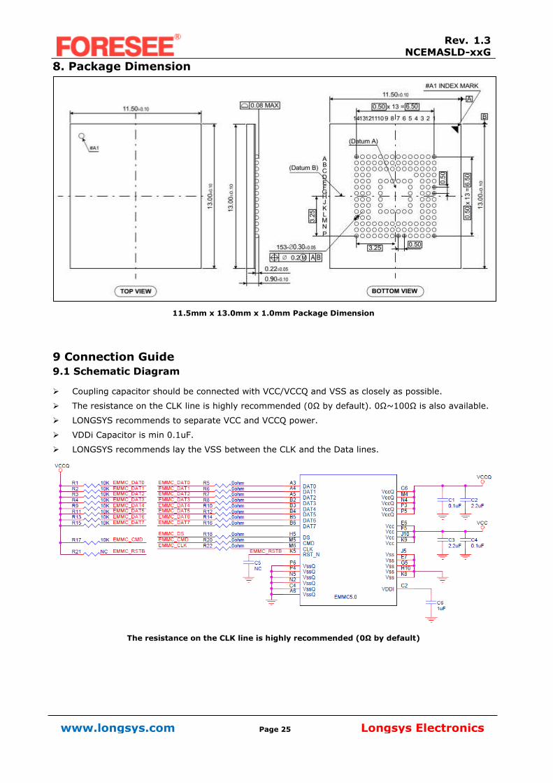
8. Package Dimension
11.5mm x 13.0mm x 1.0mm Package Dimension
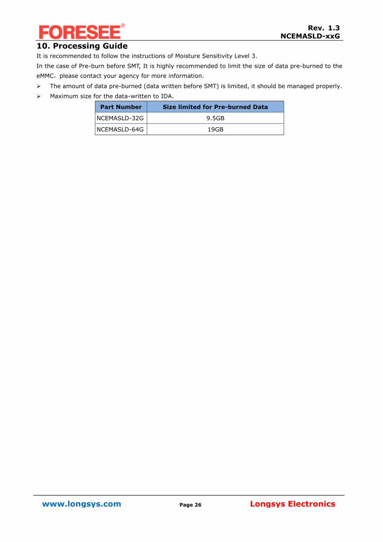
9 Connection Guide
9.1 Schematic Diagram
Coupling capacitor should be connected with VCC/VCCQ and VSS as closely as possible.
The resistance on the CLK line is highly recommended (0Ω by default). 0Ω~100Ω is also available.
LONGSYS recommends to separate VCC and VCCQ power.
VDDi Capacitor is min 0.1uF.
LONGSYS recommends lay the VSS between the CLK and the Data lines.
The resistance on the CLK line is highly recommended (0Ω by default)
www.longsys.com Page 26 Longsys Electronics
Rev. 1.3 NCEMASLD-xxG
10. Processing Guide It is recommended to follow the instructions of Moisture Sensitivity Level 3.
In the case of Pre-burn before SMT, It is highly recommended to limit the size of data pre-burned to the
eMMC,please contact your agency for more information.
The amount of data pre-burned (data written before SMT) is limited, it should be managed properly.
Maximum size for the data-written to IDA.
Part Number Size limited for Pre-burned Data
NCEMASLD-32G 9.5GB
NCEMASLD-64G 19GB


