
1
Final Project for Nanotechnology and Nanosensor course authorized by
Technion Israel Institute of Technology
Course Instructor Prof. Hossam Haick PhD
Submitted on 16th
of June 2015
Title
A conceptual framework in the design and development of embedded
nanoelectronic device with thin film Carbon Nanotube transistors, Quantum Dots
and Graphene as an artificial retinal substrate to restore vision for patients with
retinal degeneration
Submitted by
(Dr.Saravanan Subramaniam)
Project team members
1) Dr.Saravanan Subramaniam†, Post Doctoral Fellow, Department of Neurosurgery,
University Hospital Tübingen, and Centre for Integrative Neuroscience
(Neuroprosthetics), Tübingen, Germany.
2) Rogelio Federico Nochebuena†, Holds a BSEE from National Institute
Polytechnic, a MSEE from Brigham Young University and a MBA from
Pepperdine University. Research engineer at Carl Zeiss, Perkin Elmer, Xerox
PARC and Agilent Technologies.
3) Mohammad Hossein Saberi †, M.Sc. in chemical engineering, Catalysis and
Nanostructured Materials Research Laboratory, School of chemical engineering,
University of Tehran, Tehran, Iran.
(† Members contributed equally to this project)

2
Table of Contents Page No
1) Abstract
3-3
2) Introduction
4-4
3) Goal of the Project
4-4
4) Literature review
5-10
a) Current strategies for restoring vision
5-5
b) The cortical approach
5-5
c) The optic nerve approach
6-6
d) The retinal approach
6-6
e) Nanotechnology for restoration of vision
6-8
f) Characterization results of Kimura et al. work
8-10
5) Discussion and project description
10-15
a) Over all framework
10-12
b) Power supply via Inductive coupling
13-13
c) Processing of nanotubes prior placement on the inkjet cartridge
14-14
d) Nanotube characterization
14-15
e) Rendering Illumination profile
15-15
f) Animal Testing
15-15
6) Conclusions and recommendations
16-16
7) References
16-17

3
Abstract
Visual blindness affects millions of people worldwide, with varied pathogenesis and
many prevalent and potentially devastating causes of vision loss cannot be effectively
treated. In the recent years, the possibility of restoring vision to blind individuals has
been a topic of intense scientific research as well as of science fiction. Recent advances in
microelectronics have led to the development of visual prosthetic devices that are
designed to stimulate viable neuronal tissue in the hope of regaining some level of
functionality. Human clinical trials with visual prosthetic devices are underway, but it is
still in its infancy, and many technical challenges remain unsolved due to the thickness
and size of the device impeding sclera buckling and rhegmatogenous retinal detachment,
hence it’s necessary to have an alternate biocompatible device which is thin, transparent
and does not cause post implant complications. Hence, there is a compelling reason to
pursue the development of carbon nanotube thin film transistors as a viable therapeutic
option to restore vision in patients with visual blindness. Here we introduce a conceptual
idea that could potentially be very inexpensive and sensitive, the use of plastic electronics
(ink-jet technology to produce active and passive electronic devices on flexible and
transparent substrates such an electronic chip designed to convert photons from the visual
environment in to electrical signal travelling via the optic pathway terminating in the
primary and association visual cortex in the brain to restore the perception of vision.
There are several ongoing investigations addressing this issue in different parts of the
world, using microelectronic technology, which has potential adverse effects due to its
thickness and size, hence we have developed a conceptual design using thin film
transistors using carbon nanotubes, to reduce the chip size and increase the sensitivity
which could accord for reduced cost. This nanoelectronic chip is designed to be
implanted in the retina with its projections sink and encapsulates the surrounding retinal
axons which converge as a bundle to form the optic nerve traversing along its pathway to
the primary visual cortex for visual processing in the association visual cortical areas in
the brain to restore the perception of vision.

4
Introduction
Visual blindness is one of a major global public health problem. The World Health
Organization (WHO) assessed that 1% of the total global encumbrance of disease
measured as Disability-Adjusted Life Years (DALY) was assignable to vision loss [1]
.
Corresponding to the World Health Report, about 42.7 million people were assessed to be
blind and 272.4 million people have low vision [2]
. Degenerative retinal diseases such as
atrophic macular degeneration and retinitis pigmentosa can lead to severe vision loss.
While vision loss is disastrous at any age, retinitis pigmentosa often affects working-age
adults. Retinitis pigmentosa is an outer retinal degeneration that involves the retinal
pigment epithelium and the photoreceptors. Eyes with retinitis pigmentosa react to
electrical stimulation because in many patients, the inner retina and ganglion cell layer
still have some function. The existing treatment possibilities are limited and vitamins
help slow disease progression. Visual cycle modulators are in clinical trials, and initial
practice proposes they slow disease progression and may ameliorate vision in patients
with mild to moderate disease. For blind patients with light perception, or even no light
perception vision, many scientific investigators and companies around the world are
working on retinal implants in order to restore visual function, chip implants have to
detect light, convert the light energy to electrical energy, and then stimulate the retina.
Distinctive groups approach this in distinct ways [3, 4]
thin film transistor based carbon
nanotube retinal chip implants offer hope for patients with visual loss.
Goal of the Project
a) The primary goal is to design and develop a novel embedded nanoelectronic
device using thin film carbon nanotube transistors and graphene for patients with
visual blindness following retinal degeneration.
b) The secondary goal is to test the biocompatibility and functionality of the device
invivo in a sheep model prior to testing in stages of human trials.

5
Literature review
Current strategies for restoring vision
Most visual neuroprosthesis are designed upon the foundation, that focal electrical
stimulation of intact visual structures excites the sensation of distinct points of light
(‘phosphenes’) [5, 6]
. It has been assumed that geometric visual percepts can be initiated
by producing applicable multi-site patterns of electrical stimulation. The sense of shapes
and images would be sensed in a method similar to screening an electronic scoreboard in
a stadium (‘scoreboard approach’). It is widely recognized that complete maturation of
the visual system and previous visual experience are needed before a patient to be able to
properly and pertinently elucidate these visual patterns. Hence it remains indistinct if this
approach would be suitable to a patient who was blind since birth or early infancy.
The cortical approach
Basic involvement in visual prosthesis improvement was directed at stimulating the
visual cortex directly. In the late 60’s, Brindley and Lewin conducted seminal work by
chronically implanting 80 surface electrodes to overlie the visual cortex of a seriously
blind volunteer [7]
. The conveyance of electrical current to the visual cortex elicited the
sensation of distinct albeit crude forms of bright light (phosphenes). More significantly it
was ascertained that the position of these phosphenes coincided roughly to the notable
cortical topographic representation of visual space. The successive finding was of
substantial importance and recommended that anticipated patterns of light may well
potentially be formed using focal electrical stimulation. A more current attempt has
succeeded to integrate a digital video camera system that entraps and transfers encoded
visual images to the cortical stimulating array [8]
. The camera, staged onto a pair of
glasses, directs an image to a compact computer, which, in turn, decodes the signal into
suitable patterns of electrical stimulation, a number of blind volunteers have been
implanted with this device and one patient (who had been totally blind for over twenty
years) could apparently differentiate the contour of a person and recognize the orientation
of specific letters [9]
. This work has established down a consequential foundation for
constructing a feasible visual prosthesis, in spite of the fact that the cortical approach
faces a number of technical confrontations, the invasiveness of surgical implantation and
6
the risk of focal seizures induced by direct cortical stimulation present serious problems
for a patient’s safety.
The optic nerve approach
A Belgian group has lately developed a quadruplet spiral cuff electrode intended to
stimulate the optic nerve preferably than the visual cortex. The intracranial electrode was
linked to a neurostimulating circuit that is fixed to the cranium underneath down the skin
and transmits through wireless communication with an outward appearance processor and
camera. This device was chronically implanted in a 59-year-old blind volunteer. In this
patient, electrical stimulation elicited the perception of frequently colored, phosphenes in
all the visual field [10]
. After four months of practice and psychophysical testing, it was
declared that the patient could identify and differentiate directions of lines as well as
some shapes and letters [10]
contempt only a limited number of stimulating electrodes
being used.
The retinal approach
In addition to the methods mentioned above this appraoch is engaged in implanting a
stimulating device at the level of the retina. In two common causes of blindness, retinitis
pigmentosa16 and age-related macular degeneration [11]
, there is a comparatively
selective degeneration of the photoreceptor layer of the outer retina. On the other hand,
ganglion cells within the inner retinal layers survive in large numbers and react to
electrical simulation even in progressive stages of the diseases [12, 13]
. The proposition of
this retinal approach is to stimulate these cells in entity to restore lost photoreceptor
function. This procedure has the benefit of directing input more proximally alongside the
afferent visual pathway, thereby aiding from primitive physiological pre-processing and
encoding. Moreover ganglion cells are firmly packed and organized in a topographical
fashion throughout the retina. In assumption, a visual image may perhaps be generated in
a process similar to the cortical approach by directing multi-site patterns of electrical
stimulation to the ganglion cells.
Nanotechnology for restoration of vision
There are some novel phototransistors. Konstantatos et al. propose a hybrid graphene-
PbS quantum dot [13].
According to their results, covering the graphene with a colloidal
PbS quantum dots thin film leads a responsivity and electron per photon gain of about 107

7
AW-1
and 108, respectively. Actually, this ultrahigh gain originates from the high carrier
mobility of graphene sheet and the recirculation of charge carriers during the lifetime of
the carriers that remain trapped in the PbS quantum dots. A schematic of the graphene-
quantum dot hybrid phototransistor is shown in (Fig. 1).
Fig. 1. A schematic of the graphene-quantum dot hybrid phototransistor, in which a graphene flake is deposited
onto a Si/SiO2 structure and coated with PbS quantum dots [13]
In (Fig. 2) (a) the responsivity of this device as a function of the applied back-gate
voltage is plotted. They measured a responsivity as high as ~5 × 10⁷ AW
-1 when
VBG=VD, corresponding to a photoconductive gain of ~1 × 10⁸ for an excitation
wavelength of 600 nm. By tuning the Fermi energy close to the Dirac point at VBG = 4 V,
the responsivity completely falls to zero. This feature demonstrates the potential of this
device as a back-gate-tunable ultrahigh-gain phototransistor. This tunability is of great
importance in photodetectors because it allows control of the state (on-off) of the detector
as well as adjustment of the required gain, depending on the light intensity to be detected.
The back-gate tunability of the graphene Fermi level is also could be exploited to develop
reset functionality in the detectors as an electronic shutter suited to video-frame-rate
imaging applications.
They measured the sensitivity of the detector by performing differential resistance and
responsivity measurements under variable optical intensity. (Fig. 2) (b) shows the
responsivity as a function of the incident optical power on the detector area. The
responsivity remains ~1 × 10⁸
AW-1
for optical powers up to 50 fW, followed by a

8
decrease with increasing light intensity. This photocurrent saturation comes from
increasing number of photo-generated electrons [13]
.
Fig. 2. Phototransistor device characteristics. (a) Responsivity as a function of back-gate voltage, (b) Responsivity versus optical illumination power. The solid line is the best fit to the data [13].
In the term of mechanism, photon adsorption in PbS quantum dots creates electron-hole
pair separated at the graphene-quantum dot interface due to the band bending at the
interface and workfunction mismatch between graphene and quantum dots. The holes are
transferred to the graphene layer and drift by means of a voltage bias to the drain.
However, electrons remain trapped in the PbS quantum dots. As the electrons remain
trapped in the quantum dots, positive carriers in the graphene sheet are recirculated,
resulting in gain. Moreover, this device offers a gate-tunable sensitivity and speed which
is useful for pixelated imaging applications and spectral selectivity from the short-
wavelength infrared to the visible.
Characterization results of Kimura et al. work [14, 15]:
(Fig. 3) Displays, the irradiated illuminance vs output frequency. It is found that the
relationship between the irradiated illuminance and output frequency is proportional,
which is a suitable property.
Fig. 3. irradiated illuminance vs output frequency [14].

9
(Fig. 4) Displays, the detection of the irradiation distribution. Here, a light beam is
irradiated on the retinal prosthesis. It is found that the circular area where the output
frequency is higher becomes larger as the circular area where the light beam is irradiated
becomes larger. It is concluded that the irradiation distribution can be detected [14]
.
Fig. 4. detection of the irradiation distribution [14].
In the Kimura et al. work, the artificial retina using poly-Si TFTs and wireless power
supply using inductive coupling are located in a light-shield chamber, and Vout in each
retina pixel is probed by a manual prober and voltage meter. White light from a metal
halide lamp is diaphragmmed by a pinhole slit, focused through a convex lens, reflected
by a triangular prism and irradiated through the glass substrate to the back surfaces of the
artificial retina on a rubber spacer. The real image of the pinhole slit is reproduced on the
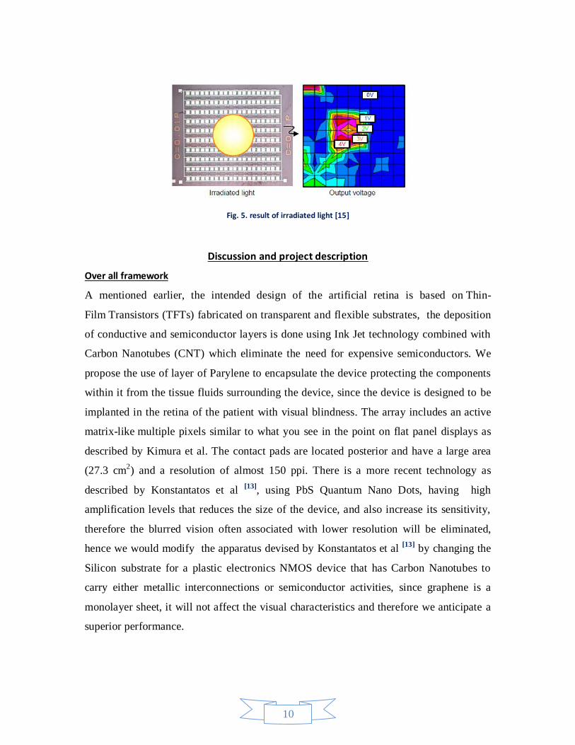
back surface. (Fig. 5) Shows the detected result of irradiated light. It is confirmed that the
Lphoto distribution can be reproduced as the Vout distribution owing to the parameter
optimization of the wireless power supply system even if it is driven using the unstable
power source, although shape distortion is slightly observed, which is due to the
misalignment of the optical system or characteristic variation of TFTs [15]
.
10
Fig. 5. result of irradiated light [15]
Discussion and project description
Over all framework
A mentioned earlier, the intended design of the artificial retina is based on Thin-
Film Transistors (TFTs) fabricated on transparent and flexible substrates, the deposition
of conductive and semiconductor layers is done using Ink Jet technology combined with
Carbon Nanotubes (CNT) which eliminate the need for expensive semiconductors. We
propose the use of layer of Parylene to encapsulate the device protecting the components
within it from the tissue fluids surrounding the device, since the device is designed to be
implanted in the retina of the patient with visual blindness. The array includes an active
matrix-like multiple pixels similar to what you see in the point on flat panel displays as
described by Kimura et al. The contact pads are located posterior and have a large area
(27.3 cm2) and a resolution of almost 150 ppi. There is a more recent technology as
described by Konstantatos et al [13]
, using PbS Quantum Nano Dots, having high
amplification levels that reduces the size of the device, and also increase its sensitivity,
therefore the blurred vision often associated with lower resolution will be eliminated,
hence we would modify the apparatus devised by Konstantatos et al [13]
by changing the
Silicon substrate for a plastic electronics NMOS device that has Carbon Nanotubes to
carry either metallic interconnections or semiconductor activities, since graphene is a
monolayer sheet, it will not affect the visual characteristics and therefore we anticipate a
superior performance.

11
.
Fig. 6. A schematic of the graphene-quantum dot hybrid phototransistor, in which a graphene flake is deposited onto a Si/SiO2 structure and coated with PbS quantum dots [13]
The retina pixel consists of a phototransistor, current mirror, and load resistance. To
optimize the phototransistor efficiency, the current mirror and load resistance are
designed to optimize the transistor performance. The photosensitivity of the reverse-
biased p/i/n poly-Si phototransistor is 150 pA at 1000 lx for white light and proper values
for all visible color lights. The mobility and the threshold voltage of the n-type and p-
type poly-Si TFT are fixed at 93 cm2 V-1s-1 , 3.6 V, 47 cm2 V -1s-1 and -2.9 V,
respectively. We anticipate that by using CNT in our design the mobility will increase
multiple times and also generate a higher photocurrent. The Fig 6.2 depicts the proposed
device including the thin-film phototransistor on a flexible substrate. When light hits the
device the following reactions takes place First, the phototransistors perceive the
irradiated light (Lphoto) and induce the photo-induced current (Iphoto). Next, the current
mirror is amplified several times Iphoto to the mirror current (Imirror). Finally, the load
resistance converts Imirror to the output voltage (Vout). Consequently, the retina pixels
irradiated with bright light output a higher Vout, whereas the retina pixels irradiated with
darker light output a lower Vout.

12
Electronic photo devices and circuits are integrated on the artificial retina, which is
implanted on the inside surface of the retina on the posterior chamber of the eye ball.
Since the irradiated light comes from one side of the artificial retina and the stimulus
signal goes out of the other side, this transparent substrate is most preferable.
Fig 6.2, illustrates the concept model of the artificial retina fabricated on a transparent substrate implanted
epiretinally.
Control
P I N
Vcontrol Vapply Anode
75nm
25nm
Lphoto Fig 6.2 PIN Thin Film Photo Transistor
Flexible & Transparent Substrate
Current Mirror
Phototransistor
Load Resistors
Vout
Fig 6.1 Schematic of a cell used to generate the pixels to stimulate the rods and cones and restore
vision
Vdd Iphoto Vdd Imirror
Biocompatible Encapsulation
L photo

13
Power supply via Inductive coupling
Power supply to the device is delivered wirelessly via inductive coupling as shown in the
(Fig 6.4). This system includes a power transmitter, power receiver, Diode Bridge, and
Zener diodes. The power transmitter consists of an ac voltage source and induction coil.
The Vpp of the ac voltage source is 10 V, and the frequency is 34 kHz, which is a
resonance frequency of this system. The material of the induction coil is an enameled
copper wire, the diameter is 1.8 cm, and the winding number is 370 times. The power
receiver also consists of an induction coil, which is the same as the power transmitter and
located face to face. The diode bridge rectifies the AC voltage to the DC voltage, and the
Zener diodes regulate the voltage value [14].
Fig 6.4. Illustrating active epiretinal nanoelectronic Implant powered by inductive coupling via RF signal.
Following the design the system should be checked for its biocompatibility and any
adverse reactions in an animal model, the supply system in principle is very simple to
implant and the generated power should also be checked for its stability. Since the
intended artificial retina is fabricated on an insulator substrate, and has little parasitic
capacitance, and is subject to influence of noise. Therefore, it is necessary to confirm
whether the artificial retina can be correctly operated even using the unstable power
source. To synthesize and ensemble the artificial retina using thin film Carbon Nanotubes
on flexible and transparent substrates we propose the following process as developed by
Sajed et al [17]
.

14
Processing of nanotubes prior placement on the inkjet cartridge
The fabrication process includes the following steps: (a) The Glass microscope slides will
be cleaned with acetone and ethanol and soft baked at 100 °C for 15 min; (b) SWCNT ink
will be printed using a Sonoplot GIX Microplotter II. Metallic SWCNT electrodes will be
printed from concentrated metallic SWCNT solution (1 mg in 10 ml aqueous solution,
Nanointegris) using a 30 μm tip. Transistor channel length of 200 μm and channel width
of 1300 μm will be printed. Metallic electrodes will be exposed in air for 24 hours and
then washed by soaking the substrate within a propriety acid wash for 24 hours. Followed
by curing at 250 °C and a next layer of metallic SWCNT will be printed over the previous
layer to increase SWCNT density of which the final sheet resistance could be obtained at
6 KΩ/square (c) Semiconducting SWCNT solution (1 mg in 100 ml aqueous solution,
Nanointegris) will be printed with a 30 μm tip to complete the transistor change. Clean
semiconducting SWCNT films will be obtained by soaking the printed substrate in a
propriety acid for 24 hours; (d) the ionic gel solution of PS-PMMA-PS (1.5%, weight)
and EMIM TFSI (8.5%, weight) in ethyl acetate will be prepared and supplied. Since the
ionic gel has a high viscosity, it will be printed using a 500 μm in diameter tip in order to
print a uniform and transparent layer of gel over the channel. The device will then be
cured at a temperature of 105 °C for 1 hour. After this process, all-SWCNT TFT
fabricated devices will then be subsequently tested [17]
.
Nanotube characterization
We intend to test the nanotubes using SEM (scanning electron microscope), DTA
(Differential Thermal Analysis), High-Energy Milling devices, Spark Plasma Sintering
and extrusion techniques soft chemistry (sol-gel) among others which will be decided
based on its feasibility with this intended protocol.
For electronic characterization, we intend to use four point probes, capacitance,
inductance, and frequency responses using impedance, network and spectrum analyzer.
Of course, the need for some specialized test rigs to check electrical connections is quite
obvious and it’s included in the protocol.
Mechanical test include Young’s Module, thermal conductivity, elongation, stiffness,
hardness. We make sure to use proper rigs to ensure that the testing is accurate. Optically

15
speaking we can conduct test such as electro-luminescence, transmission, reflection,
fluorescence, refractive index, transparency and for chemical testing we intend to include
testing the pH level and spectroscopy.
Rendering Illumination profile
The Vout in each retina pixel will be probed by a manual prober and voltage meter. White light
from a metal halide lamp will be diaphragmmed by a pinhole slit, focused through a convex lens,
reflected by a triangular prism and irradiated through the glass substrate to the back surfaces of
the artificial retina on a rubber spacer. The real image of the pinhole slit will be reproduced on the
back surface [15, 16].
Animal Testing
Retinal degeneration will be induced in the sheep by retinoid cycle impairment prior to
the implant and once the embedded nanoelectronic retinal device is fabricated, the
functionality and the biocompatibility will be tested in a sheep, after induction of general
anesthesia, local infiltration with lidocaine will be delivered along the line of zygomatic
arch and a small incision will be made on the posterior rim of the orbit along the line of
zygomatic arch and the subcutaneous tissue will be retracted and fixed by clamps,
bleeding will be arrested by a bipolar electrocauterization and a small burr hole will be
made with an electric burr on the posterior rim of the orbit, then a trans sclera choroidal
microincision will be made and the fabricated transparent thin film carbon nanotube
embedded nanoelectronic retinal device will be implanted in the retinal surface as shown
in the (Fig.7). The probe for power transfer via RF signal will be packed subcutaneously
with a pocket incision along the mastoid process.
Fig.7. Illustrates the embedded nanoelectronic implant device invivo in the retinal surface of a sheep

16
Conclusions and Recommendations
We propose that epiretinal implantation of this novel embedded nanoelectronic device
with enhanced capabilities augmented by Carbon Nanotubes and Quantum Dots,
combined with Graphene are able to generate electronic signals that our brain interprets
as natural stimulation to trigger neurons in the primary and association visual cortex, to
alleviate symptoms of visual blindness arising as a sequelae in patients with retinitis
pigmentosa and progressive macular degeneration. Prior to be used in humans we
recommend to test the biocompatibility of the devise and for any adverse complications
such as endophthalmitis, conjunctival erosion, and retinal hemorrhage arising from the
implant itself in vivo in a sheep model prior to stages of clinical trials in human subjects
with visual blindness as a sequelae of retinal degeneration.
References
1) World Health Organization. World Health Report 2004. Changing History.
Geneva: 2004. table 3 p130.
2) The Global Burden of Disease: 2004 update World Health organization.
(http://www.who.int/healthinfo/global_burden_disease/2004_report_update/en/)
3) Weiland JD, Cho AK, Humayun MS. Retinal Prosthesis: current clinical results
and future needs. Ophthalmology; 118:2227-37 (2011).
4) Rizzo JF, Shire DB, Kelly SK, et al. Overview of the Boston Retinal Prosthesis:
Challenges and opportunities to restore useful vision to the blind. Conf Proc IEEE
Eng Med Biol Soc; 2011:7492-5 (2011).
5) Marg, E. & Rudiak, D. Phosphenes induced by magnetic stimulation over the
occipital brain: description and probable site of stimulation. Optom. Vis. Sci. 71,
301–311 (1994).
6) Gothe, J. et al. Changes in visual cortex excitability in blind subjects as
demonstrated by transcranial magnetic stimulation. Brain 125, 479–490 (2002).
7) Brindley, G. S. & Lewin, W. S. The sensations produced by electrical stimulation
of the visual cortex. J. Physiol. (Lond.) 196, 479–493 (1968).
8) Dobelle, W. H. Artificial vision for the blind by connecting a television camera to
the visual cortex. ASAIO J. 46, 3–9 (2000)

17
9) Veraart, C., Wanet-Defalque, M. C., Gerard, B., Vanlierde, A. & Delbeke, J.
Pattern recognition with the optic nerve visual prosthesis. Artif. Organs 27(11),
996–1004 (2003).
10) Hims, M. M., Diager, S. P. & Inglehearn, C. F. Retinitis pigmentosa: genes,
proteins and prospects. Dev. Ophthalmol. 37, 109–125 (2003).
11) Loewenstein, J. I., Montezuma, S. R. & Rizzo, J. F. Outer retinal degeneration: an
electronic retinal prosthesis as a treatment strategy. Arch. Ophthalmol. 122, 587–
596 (2004).
12) Humayun, M. S. et al. Visual perception elicited by electrical stimulation of retina
in blind humans. Arch. Ophthalmol. 114, 40–46 (1996).
13) Konstantatos, G, Badioli, M, Gaudreau, L, Osmond, J, Bernechea, M, Arquer,
FG, Gatti, F, Koppens, “Hybrid graphene-quantum dot phototransistors with
ultrahigh gain”. Nature Nanotechnology 7, 363-368 (2012).
14) M. Kimura , Y. Miura , T. Ogura , S. Ohno , T. Hachida , Y. Nishizaki , T.
Yamashita and T. Shima "Device characterization of p/i/n thin-film
phototransistor for photosensor applications", IEEE Electron Device Lett., vol.
31, no. 9, pp.984 -986 (2010).
15) Y. Miura, T. Hasida, M. Kimura. “Artificial Retina Using Thin-Film Transistors
Driven by Wireless Power Supply” IEEE Sensors Journal. , vol 11, no. 7, pp
1564-1567, (2011).
16) A.Caspi , J. D. Dorn , K. H. McClure , M. S. Humayun , R. J. Greenberg and M.
J. McMahon "Feasibility study of a retinal prosthesis", Arch. Ophthalmol., vol.
127, pp.398 -401 (2009).
17) Sajed, F.; Rutherglen, C. "All-printed and transparent single walled carbon
nanotube thin film transistor devices". Applied Physics Letters 103 (14): 143303
(2013).


![SEQUENTIALMONTECARLOTECHNIQUES … · —JOHNH.HALTON—SEQUENTIALMONTECARLOFORLINEARSYSTEMS— — 6— manyofthestatisticalpropertiesoftrulyrandomsequences],inparalleland treestructuredseries,16and](https://cdn.vdocuments.mx/doc/165x107/5f2040e4ed5b2c016d4e3fbc/sequentialmontecarlotechniques-ajohnhhaltonasequentialmontecarloforlinearsystemsa.jpg)


