
ii
EXPERIMENTAL DEMONSTRATION OF CAP TRANSMITTER USING VERY
HIGH SPEED IC HARDWARE DESCRIPTION LANGUAGE (VHDL)
YUSMAHAIDA BINTI YUSOFF
A thesis submitted in
fulfillment of the requirement for the award of the
Degree of Master of Electrical Engineering
Faculty of Electrical and Electronic Engineering
Universiti Tun Hussein Onn Malaysia
AUGUST 2015
vi
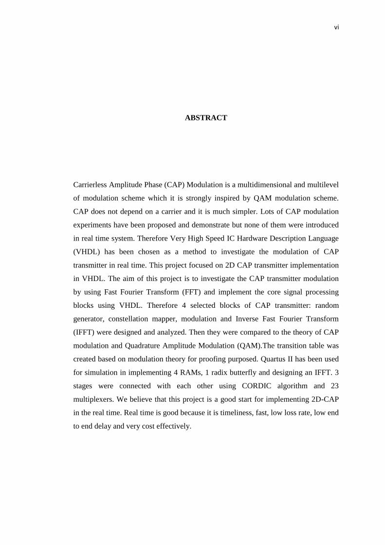
ABSTRACT
Carrierless Amplitude Phase (CAP) Modulation is a multidimensional and multilevel
of modulation scheme which it is strongly inspired by QAM modulation scheme.
CAP does not depend on a carrier and it is much simpler. Lots of CAP modulation
experiments have been proposed and demonstrate but none of them were introduced
in real time system. Therefore Very High Speed IC Hardware Description Language
(VHDL) has been chosen as a method to investigate the modulation of CAP
transmitter in real time. This project focused on 2D CAP transmitter implementation
in VHDL. The aim of this project is to investigate the CAP transmitter modulation
by using Fast Fourier Transform (FFT) and implement the core signal processing
blocks using VHDL. Therefore 4 selected blocks of CAP transmitter: random
generator, constellation mapper, modulation and Inverse Fast Fourier Transform
(IFFT) were designed and analyzed. Then they were compared to the theory of CAP
modulation and Quadrature Amplitude Modulation (QAM).The transition table was
created based on modulation theory for proofing purposed. Quartus II has been used
for simulation in implementing 4 RAMs, 1 radix butterfly and designing an IFFT. 3
stages were connected with each other using CORDIC algorithm and 23
multiplexers. We believe that this project is a good start for implementing 2D-CAP
in the real time. Real time is good because it is timeliness, fast, low loss rate, low end
to end delay and very cost effectively.

vii
ABSTRAK
Modulasi Carrierless Amplitude Phase (CAP) tergolong dalam pelbagai dimensi dan
pelbagai aras skim modulasi yang mana ianya banyak dipengaruhi oleh skim
Quadrature Amplitude Modulation (QAM). CAP tidak bergantung kepada pembawa
malah ianya sangat ringkas. Pelbagai kaji selidik terhadap modulasi CAP telah
dijalankan dan didemonstrasikan namun tiada satu daripadanya mengkaji dalam
masa yang sebenar. Oleh itu Very High Speed IC Hardware Description Language
(VHDL) telah dipilih sebagai kaedah untuk mengkaji modulasi penghantar CAP
dalam masa yang sebenar. Fokus projek ini adalah menjurus kepada penghantar 2D
CAP yang dilaksanakan menggunakan VHDL. Tujuan projek ini dilaksanakan
adalah untuk mengkaji modulasi penghantar CAP dengan menggunakan Inverst Fast
Fourier Transform (IFFT) dan menghasilkan blok asas bagi proses isyarat dengan
bantuan VHDL. Justeru itu, 4 blok penghantar CAP: penjana rawak, buruj mapper,
proses modulasi dan juga IFFT telah direka dan dianalisa. Keempat-empat blok telah
dibandingkan dengan teori modulasi CAP dan juga modulasi QAM. Jadual peralihan
telah dibangunkan berdasarkan teori untuk tujuan pembuktian. Quartus II telah
digunakan sebagai simulasi bagi melaksanakan sistem 4 RAM, 1 radix butterfly dan
merekacipta IFFT. 3 peringkat telah disambung antara satu sama lain menggunakan
algoritma CORDIC dan juga dengan bantuan 23 pemultipleks. Kami percaya projek
ini merupakan satu permulaan projek yang bagus untuk melaksanakan 2D-CAP di
dalam masa yang sebenar. Masa yang sebenar amat bagus keranaianya mempunyai
ketepatan masa. Kadar kehilangan yang rendah, lajakan yang rendah dan kos yang
sangat effektif.

viii
TABLE OF CONTENTS
THESIS STATUS CONFIRMATION
TITLE ii
AUTHOR’S DECLARATION iii
DEDICATION iv
ACKNOWLEDGEMENT v
ABSTRACT vi
CONTENTS viii
LIST OF TABLES xii
LIST OF FIGURES xiii
LIST OF SYMBOLS AND ABBREVIATIONS xv
CHAPTER 1 INTRODUCTION 1
1.1 Project Background 1
1.2 Problem Statement 6
1.3 Objectives 6
1.4 Scope 6
1.5 Report Outline 6
1.6 Summary of work 7
ix
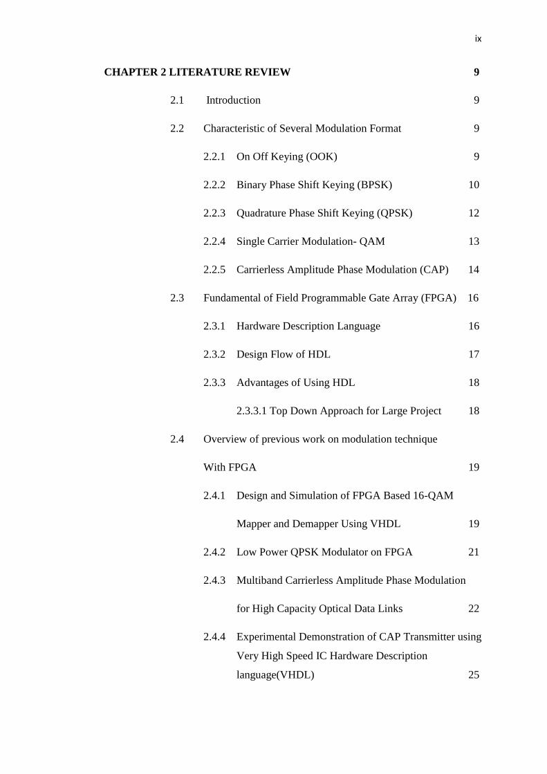
CHAPTER 2 LITERATURE REVIEW 9
2.1 Introduction 9
2.2 Characteristic of Several Modulation Format 9
2.2.1 On Off Keying (OOK) 9
2.2.2 Binary Phase Shift Keying (BPSK) 10
2.2.3 Quadrature Phase Shift Keying (QPSK) 12
2.2.4 Single Carrier Modulation- QAM 13
2.2.5 Carrierless Amplitude Phase Modulation (CAP) 14
2.3 Fundamental of Field Programmable Gate Array (FPGA) 16
2.3.1 Hardware Description Language 16
2.3.2 Design Flow of HDL 17
2.3.3 Advantages of Using HDL 18
2.3.3.1 Top Down Approach for Large Project 18
2.4 Overview of previous work on modulation technique
With FPGA 19
2.4.1 Design and Simulation of FPGA Based 16-QAM
Mapper and Demapper Using VHDL 19
2.4.2 Low Power QPSK Modulator on FPGA 21
2.4.3 Multiband Carrierless Amplitude Phase Modulation
for High Capacity Optical Data Links 22
2.4.4 Experimental Demonstration of CAP Transmitter using
Very High Speed IC Hardware Description
language(VHDL) 25

x
CHAPTER 3 METHODOLOGY 26
3.1 Introduction 26
3.2 CAP Modulation 27
3.2.1 Mapping 28
3.2.2 Upsampling 28
3.2.3 Convolution 28
3.2.4 Fast Fourier Transform (FFT) 29
CHAPTER 4 RESULT AND ANALYSIS 30
4.1 Introduction 30
4.2 Random Generator 31
4.2.1 CAP random generator 31
4.2.2 Result for Random generator 32
4.3 CAP Constellation Mapper 33
4.3.1 Mapper 34
4.3.2 Serial To Parallel 34
4.3.3 CAP Modulator 36
4.4 IFFT 38
4.4.1 CAP IFFT Algorithm 36
4.4.2 CAP IFFT Result 40
CHAPTER 5 CONCLUSION 43
5.1 Conclusion 43
5.1.1 Design CAP Transmitter modulation using IFFT 43
5.1.2 Simulate the Core Signal Processing Blocks of

xi
CAP Transmitter Using VHDL Language 44
5.2 Future Work 44
5.2.1 Receiver CAP Modulation Using VHDL
Language 44
5.2.2 High Dimensionality of CAP system in FPGA
Platform 44
REFERENCES 45
xii
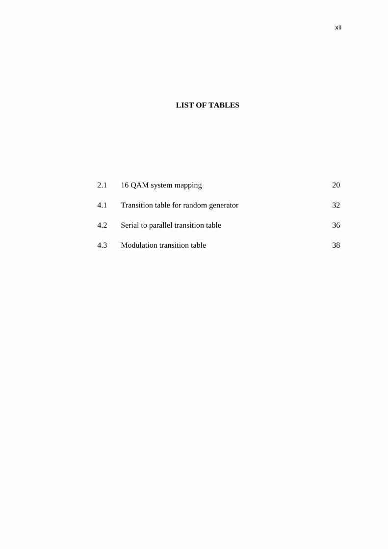
LIST OF TABLES
2.1 16 QAM system mapping 20
4.1 Transition table for random generator 32
4.2 Serial to parallel transition table 36
4.3 Modulation transition table 38
xiii
LIST OF FIGURES
1.1 Modulation of digital signal of amplitude shift keying (ASK) 2
1.2 FSK modulation. Binary data (a) Frequency modulates the
Carrier to produce the FSK signal (b) Which has the frequency
Characteristic (c). 3
1.3 Modulation of digital signal of phase shift keying (PSK) 4
1.4 Quadrature amplitude modulation (QAM) 5
1.5 Project work flow 8
2.1 On Off Keying (OOK) modulation 10
2.2 One dimension constellation diagram 10
2.3 A block diagram of BPSK modulator 11
2.4 BPSK modulation 11
2.5 Block diagram of a QPSK modulator 12
2.6 QPSK constellation diagram 12
2.7 Output phases versus time relationship for a QPSK modulator 13
2.8 8 QAM (a) Block diagram (b) Truth table 13
2.9 8 QAM constellations 14
2.10 Block diagram of CAP modulator 15
xiv
2.11 16 CAP constellations 15
2.12 FPGA design flow 17
2.13 QAM transmitter block diagram 19
2.14 QAM receiver block diagram 20
2.15 Simulation of 16 QAM mapper and demapper in Quartus II 21
2.16 Proposed block diagram of QPSK modulator 22
2.17 Optical simulation setup 23
2.18 Experiment setup 23
2.19 (a) BER Curves (b) transmitter bandwith tolerance (c) chromatic
Dispersion tolerance and (d) RIN tolerance 24
2.20 (a) Frequency response pre-DAC signal spectrum (b) Optical
Spectrums and (c) BER curves 24
3.1 Block diagram of two dimensional (2D) CAP modulations 26
3.2 Register Transfer Level (RTC) schematic of CAP transmitter 27
4.1 Block diagram of CAP transmitter 30
4.2 RTL schematic for CAP random generator 31
4.3 The output of CAP random generator 31
4.4 Block diagram QAM random generator 32
4.5 Random input bit stream generated in VHDL 33
4.6 Block diagram of constellation mapper 33
4.7 Constellation block interconnection for CAP modulator 33
4.8 Constellation diagram 34
4.9 Serial to parallel block 35
xv
4.10 The output serial to parallel shift register 35
4.11 Modulation block 36
4.12 Output of the CAP modulation 37
4.13 IFFT for 8 inputs 39
4.14 Block interconnection for IFFT 40
4.15 RTL schematic for IFFT modulation 41
4.16 Output from IFFT 41

xvi
LIST OF SYMBOLS AND ABBREVIATIONS
ASK - Amplitude Shift Keying
FSK - Frequency Shift Keying
PSK - Phase Shift Keying
PAM - Pulse Amplitude Modulation
QAM - Quadrature Amplitude Modualtion
CAP - Carrierless Amplitude Phase
GbE - Gb Ethernet
FPGA - Field programmable gate arrays
VHDL - Very High Speed IC Hardware Description Language
IFFT - Inverse Fast Fourier Transform
OOK - On Off Keying
BPSK - Binary Phase Shift Keying
QPSK - Quadrature Phase Shift Keying
DAC - Digital to Analog Converter
LPF - Low Pass Filter
IJSETR - International Journal of Science, Engineering and Technology
Research
SIPO - Serial input parallel output
DSO - Digital Signal Oscilloscope
EML - External Modulator laser
PD - Photodiode
2D - 2 Dimensional
LFSR - Linear Feedback Shift Register
FSM - Finite State Machine
DFT - Discrete Fourier Transform
RAM - Random Access Memory
CHAPTER 1
INTRODUCTION
1.1 PROJECT BACKGROUND
The fiber optic communication actually started since 1790s when French engineer,
Claude Chappe, who invented the “Optical telegraph” introduced a series of
semaphores which mounted on towers. Then, communication technology become
popular when optical telephone system was introduced by Alexander Graham Bell in
1880. Apart of it, new technology slowly took place to solve the optical transmission
problem. In 1930s, Heinrich Lamm the first person demonstrated image transmission
through a bundle of optical fiber [1]. This is the starting step where fiber optic starts
its revolution. The new technology was introduced year by year in order to make sure
the network is stable, give the highest speed of transmission and at the same time it is
efficient.
Not only the technology has changes but the modulation technique also has
their revolution. They were upgraded to new phase which using digital technique
instead of analog technique. Digital modulation has two main categories which are
amplitude/phase modulation and frequency modulation. Basically frequency
modulation is known as nonlinear modulation or constant envelope modulation while
amplitude/phase modulation is called linear modulation.
Linear modulation generally has better spectral properties than nonlinear
modulation, since nonlinear processing leads to spectral broadening [2]. The
constellation size must be chosen once modulation technique is determined. The
larger constellation size, the higher data rates it is.
2
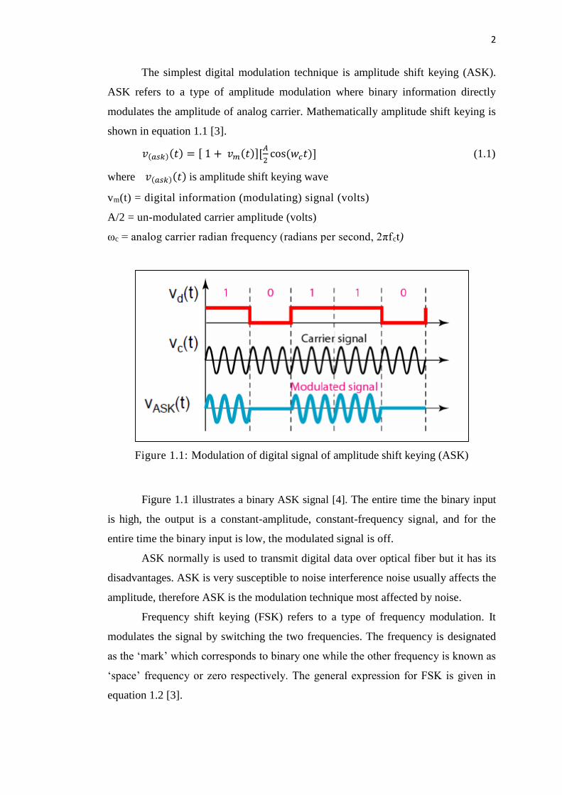
The simplest digital modulation technique is amplitude shift keying (ASK).
ASK refers to a type of amplitude modulation where binary information directly
modulates the amplitude of analog carrier. Mathematically amplitude shift keying is
shown in equation 1.1 [3].
𝑣(𝑎𝑠𝑘)(𝑡) = [ 1 + 𝑣𝑚(𝑡)][𝐴
2cos (𝑤𝑐𝑡)] (1.1)
where 𝑣(𝑎𝑠𝑘)(𝑡) is amplitude shift keying wave
vm(t) = digital information (modulating) signal (volts)
A/2 = un-modulated carrier amplitude (volts)
ωc = analog carrier radian frequency (radians per second, 2πfct)
Figure 1.1: Modulation of digital signal of amplitude shift keying (ASK)
Figure 1.1 illustrates a binary ASK signal [4]. The entire time the binary input
is high, the output is a constant-amplitude, constant-frequency signal, and for the
entire time the binary input is low, the modulated signal is off.
ASK normally is used to transmit digital data over optical fiber but it has its
disadvantages. ASK is very susceptible to noise interference noise usually affects the
amplitude, therefore ASK is the modulation technique most affected by noise.
Frequency shift keying (FSK) refers to a type of frequency modulation. It
modulates the signal by switching the two frequencies. The frequency is designated
as the ‘mark’ which corresponds to binary one while the other frequency is known as
‘space’ frequency or zero respectively. The general expression for FSK is given in
equation 1.2 [3].
3
𝑣(𝑓𝑠𝑘)(𝑡) = 𝑉𝑐cos { 2𝜋 [𝑓𝑐 + 𝑣𝑚(𝑡)∆𝑓]𝑡} (1.2)
where 𝑣(𝑓𝑠𝑘)(𝑡)is binary FSK waveform
Vc= peak analog carrier center frequency (volts)
Δf = peak change (shift) in the analog carrier frequency
fc= analog carrier center frequency (hertz)
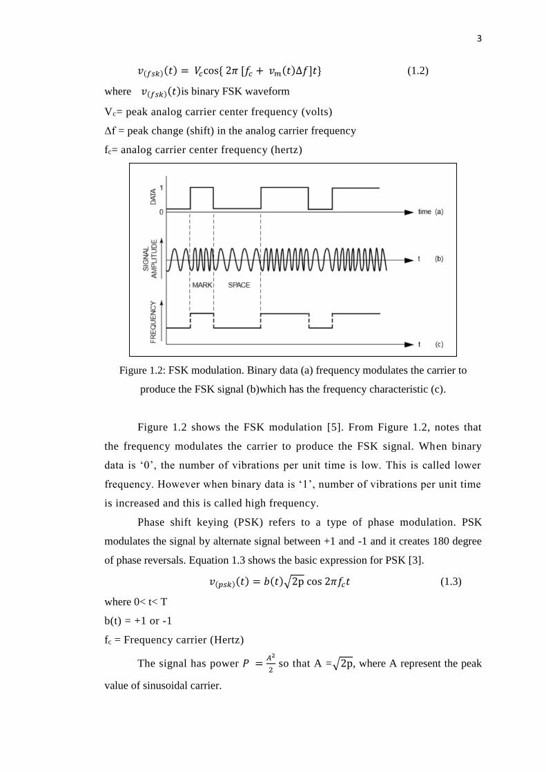
Figure 1.2: FSK modulation. Binary data (a) frequency modulates the carrier to
produce the FSK signal (b)which has the frequency characteristic (c).
Figure 1.2 shows the FSK modulation [5]. From Figure 1.2, notes that
the frequency modulates the carrier to produce the FSK signal. When binary
data is ‘0’, the number of vibrations per unit time is low. This is called lower
frequency. However when binary data is ‘1’, number of vibrations per unit time
is increased and this is called high frequency.
Phase shift keying (PSK) refers to a type of phase modulation. PSK
modulates the signal by alternate signal between +1 and -1 and it creates 180 degree
of phase reversals. Equation 1.3 shows the basic expression for PSK [3].
𝑣(𝑝𝑠𝑘)(𝑡) = 𝑏(𝑡)√2p cos 2𝜋𝑓𝑐𝑡 (1.3)
where 0< t< T
b(t) = +1 or -1
fc = Frequency carrier (Hertz)
The signal has power 𝑃 =𝐴2
2 so that A =√2p, where A represent the peak
value of sinusoidal carrier.

4
Figure 1.3: Modulation of digital signal of phase shift keying (PSK)
Figure 1.3 shows the modulation of digital signal of phase shift keying [6]. It
is called phase shift keying when modulated signal has difference phase. Look at the
transition between data ‘0’ and ‘1’. There is a phase shift at 180 degrees and the
waveforms are mirror images with each other.
The general principles of signal space analysis will then be applied to the
analysis of amplitude and phase modulation techniques, including Pulse Amplitude
modulation (PAM), Phase-shift keying (PSK) and Quadrature amplitude modulation
(QAM) [7]. QAM function does not appear the same within each symbol period due
to presence of the sinusoidal functions and potential arbitrary choice of a carrier
frequency. Usually QAM basic function have non periodic symbol rate, even they
keep repeating transmit the same message. It has two dimensional signaling as shown
in Figure 1.4 [4]. However QAM have same spectrum efficiency and need a splitter.

5
Figure 1.4: Quadrature amplitude modulation (QAM).
The carrier modulation in QAM is superfluous due to 2 dimensional basic
modulations. Although periodicity is not a big issue, but the usage of it can allow
minor simplification in implementation in few cases like Carrierless Amplitude
Phase (CAP) modulation.
CAP is a multi-dimensional and multi-level signal format employing
orthogonal waveforms [8]. The CAP modulations are the vibrational scheme of
QAM for single carrier systems [9]. As the technology changes, the inventor start to
implement digital technique because digital are more real time compared to analog.
Real time in communication means user can exchange information instantly.
We believe that in future the investigation of 10-Gb Ethernet (GbE) in real
time systems using field-programmable gate arrays (FPGAs) can be potentially
attractive candidate for optical fiber system using multi-dimensional CAP [10]. This
project is focus on CAP modulation using FPGA with VHDL.
6
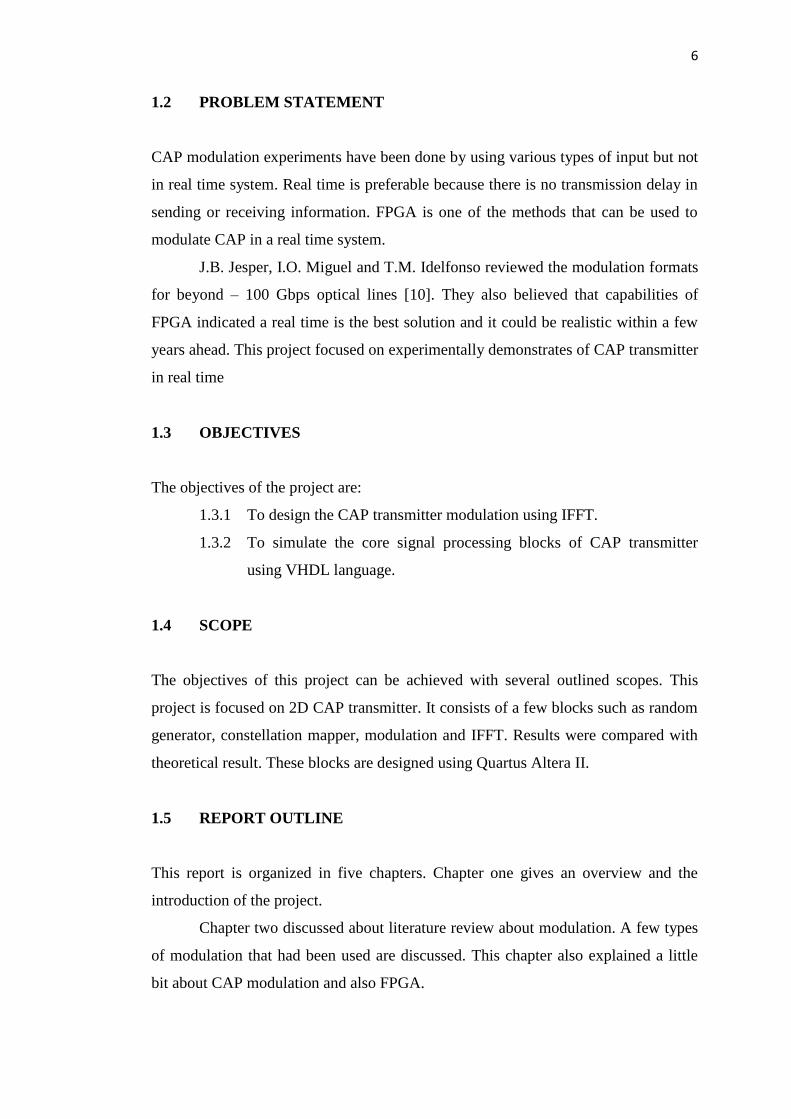
1.2 PROBLEM STATEMENT
CAP modulation experiments have been done by using various types of input but not
in real time system. Real time is preferable because there is no transmission delay in
sending or receiving information. FPGA is one of the methods that can be used to
modulate CAP in a real time system.
J.B. Jesper, I.O. Miguel and T.M. Idelfonso reviewed the modulation formats
for beyond – 100 Gbps optical lines [10]. They also believed that capabilities of
FPGA indicated a real time is the best solution and it could be realistic within a few
years ahead. This project focused on experimentally demonstrates of CAP transmitter
in real time
1.3 OBJECTIVES
The objectives of the project are:
1.3.1 To design the CAP transmitter modulation using IFFT.
1.3.2 To simulate the core signal processing blocks of CAP transmitter
using VHDL language.
1.4 SCOPE
The objectives of this project can be achieved with several outlined scopes. This
project is focused on 2D CAP transmitter. It consists of a few blocks such as random
generator, constellation mapper, modulation and IFFT. Results were compared with
theoretical result. These blocks are designed using Quartus Altera II.
1.5 REPORT OUTLINE
This report is organized in five chapters. Chapter one gives an overview and the
introduction of the project.
Chapter two discussed about literature review about modulation. A few types
of modulation that had been used are discussed. This chapter also explained a little
bit about CAP modulation and also FPGA.

7
Chapter three explains the design methodology of the project. The design
overview and block diagram are also discussed.
Chapter four discussed the result of CAP transmitter modulation using VHDL
language while Chapter five is summarizing overall of this project.
1.6 SUMMARY OF WORK
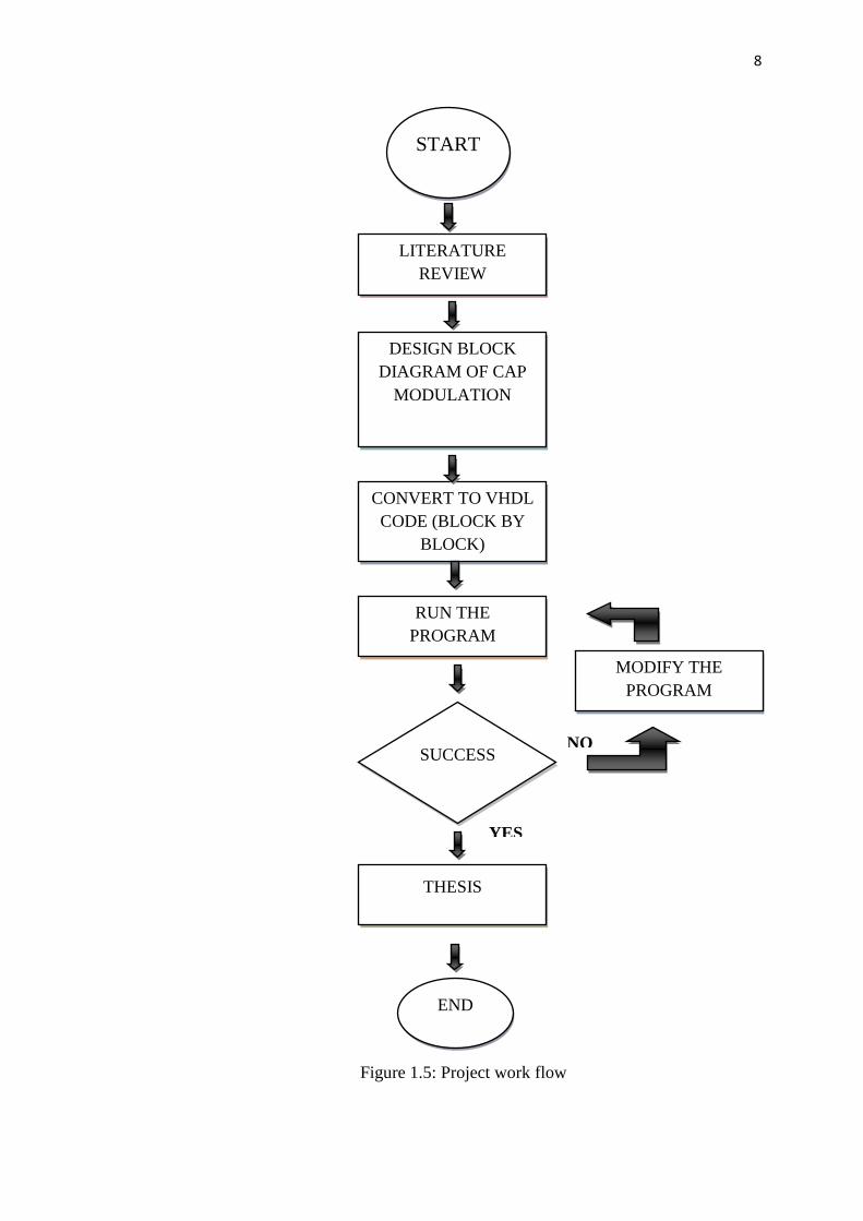
The project flow is outlined as illustrated in Figure 1.5. The project begins with
literature review. Literature review will covered some of advanced modulation
format, CAP and also FPGA. The generation for each topic together with their
advantages and disadvantages were also stated. Then it is followed by designing the
block diagram of CAP modulation. Block diagram consists of two parts which are
transmitter and also receiver.
Each block will be converted to VHDL code. At this phase, input sources
need to be declared together with parameters. The programs for each block will be
tested by running the VHDL code. If there is an error, VHDL code and structure of
the program will be modified in order to fix it. The last step of the project is writing
thesis.
8
Figure 1.5: Project work flow
START
LITERATURE
REVIEW
DESIGN BLOCK
DIAGRAM OF CAP
MODULATION
CONVERT TO VHDL
CODE (BLOCK BY
BLOCK)
THESIS
SUCCESS
RUN THE
PROGRAM
MODIFY THE
PROGRAM
END
YES
NO

9
CHAPTER 2
LITERATURE REVIEW
2.1 INTRODUCTION
In this chapter, the definition of high dimensionality is explained. The advantages of
high dimensionality modulation and also the techniques that have been used will be
discussed.
2.2 CHARACTERISTIC OF SEVERAL MODULATION FORMATS
There are generations of modulation formats that involve in communication system.
The explanation consists of their structure, advantages and also disadvantages.
2.2.1 ON OFF KEYING (OOK)
On Off Keying [11] or known as OOK is commonly used few years back. OOK is
the simplest modulation format where it used logical ‘1’ and ‘0’ to represent the on
and off data as shown in Figure 2.1. The optical power is modulated according to the
binary input signal.
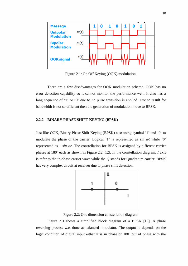
10
Figure 2.1: On Off Keying (OOK) modulation.
There are a few disadvantages for OOK modulation scheme. OOK has no
error detection capability so it cannot monitor the performance well. It also has a
long sequence of ‘1’ or ‘0’ due to no pulse transition is applied. Due to result for
bandwidth is not so efficient then the generation of modulation move to BPSK.
2.2.2 BINARY PHASE SHIFT KEYING (BPSK)
Just like OOK, Binary Phase Shift Keying (BPSK) also using symbol ‘1’ and ‘0’ to
modulate the phase of the carrier. Logical ‘1’ is represented as sin ɷt while ‘0’
represented as – sin ɷt. The constellation for BPSK is assigned by different carrier
phases at 180º each as shown in Figure 2.2 [12]. In the constellation diagram, I axis
is refer to the in-phase carrier wave while the Q stands for Quadrature carrier. BPSK
has very complex circuit at receiver due to phase shift detection.
Figure 2.2: One dimension constellation diagram.
Figure 2.3 shows a simplified block diagram of a BPSK [13]. A phase
reversing process was done at balanced modulator. The output is depends on the
logic condition of digital input either it is in phase or 180º out of phase with the
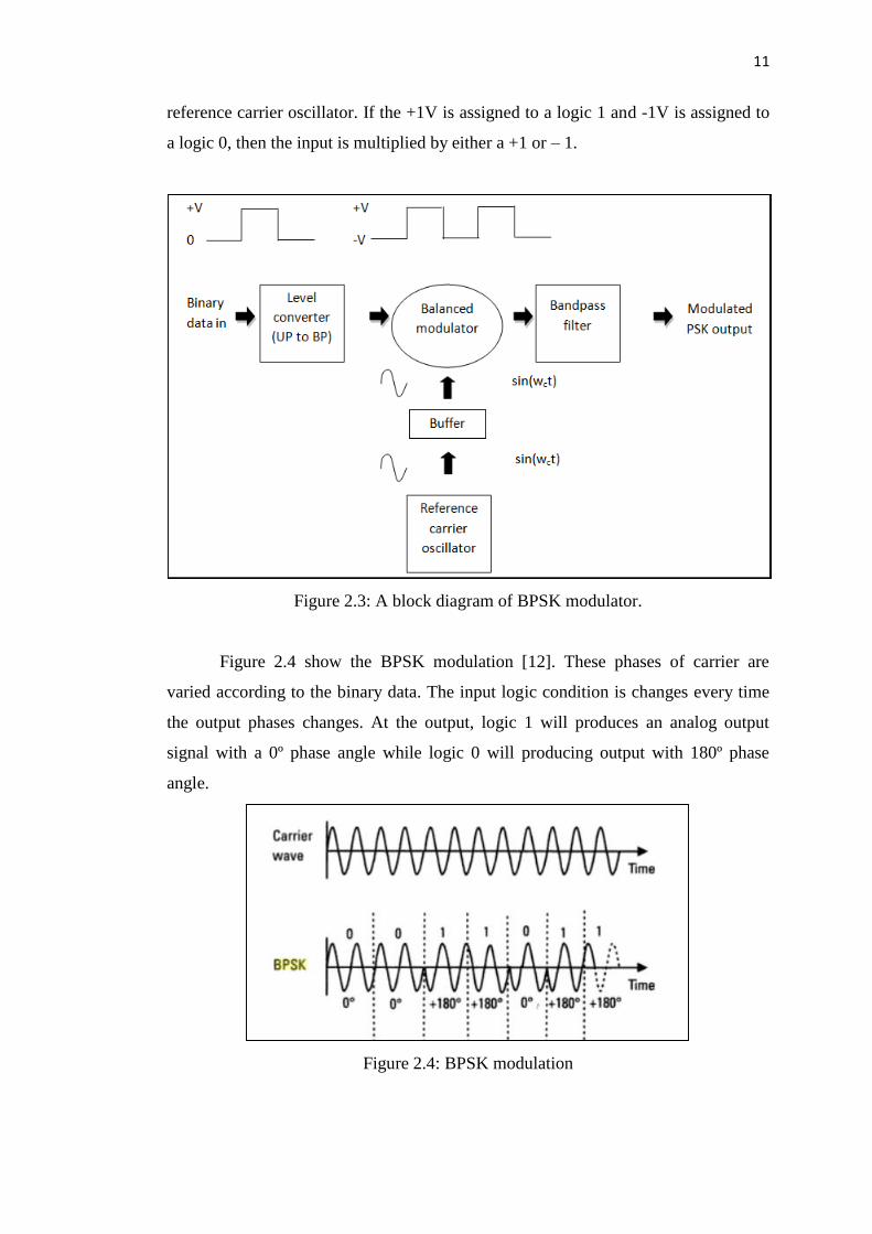
11
reference carrier oscillator. If the +1V is assigned to a logic 1 and -1V is assigned to
a logic 0, then the input is multiplied by either a +1 or – 1.
Figure 2.3: A block diagram of BPSK modulator.
Figure 2.4 show the BPSK modulation [12]. These phases of carrier are
varied according to the binary data. The input logic condition is changes every time
the output phases changes. At the output, logic 1 will produces an analog output
signal with a 0º phase angle while logic 0 will producing output with 180º phase
angle.
Figure 2.4: BPSK modulation

12
2.2.3 QUADRATURE PHASE SHIFT KEYING (QPSK)
Figure 2.5 show a block diagram of a Quadrature Phase Shift Keying (QPSK)
modulator [13]. Bit splitter acts as an input clocked of 2 bits. The input was clocked
in serial and they were simultaneously in parallel at output. They have 2 bits of input
I and Q which I is in phase with reference oscillator while Q is 90º out of phase.
Figure 2.5: Block diagram of a QPSK modulator.
For I balanced modulator, 2 phases are possible is + sin 𝑤𝑐 𝑡 and - sin 𝑤𝑐 𝑡
and for Q balanced modulator, 2 phases are possible is +cos 𝑤𝑐 𝑡 and - cos 𝑤𝑐 𝑡.
Linear summer will combined the 2 quadrature signal and yet 4 possible phases acts
as an output as shown in Figure 2.6. The four combinations of two bits are 00, 01,
10, and 11.
Figure 2.6: QPSK constellation diagram.

13
These 4 combinations are generated by 4 phase changes: -45º, +135º, -45º and
-135º radians with respect to I and Q axes as shown in Figure 2.7 [13].
Figure 2.7: Output phases versus time relationship for a QPSK modulator.
2.2.4 SINGLE CARRIER MODULATION-QAM
Quadrature Amplitude Modulation or QAM is a single carrier modulation. It was
generated by quartz implemented. It consists of an amplitude and phase modulation
of a single carrier. Every n bits duration is correspond to amplitude and phase once
the carrier ɷ0 is modulated. QAM has different types of constellations. Some of the
constellations are called 4-QAM, 8-QAM, 16-QAM and 64-QAM based on the
nearest point to origin. For example the 4-QAM constellation is limited to the 4
nearest points around the origin. Once the constellation is increased, the number of
amplitude and phase also increased. It also affected to frequency utilization where it
is more efficient and is expressed in bits per second per hertz.
Figure 2.8: 8-QAM (a) Block diagram; (b) Truth table.
14
A block diagram of an 8-QAM is shown as in Figure 2.8 (a) [13]. There is
slightly different between 8-QAM and 8-QPSK which is the omission of the inverter
between C channel and Q product modulator. The incoming data was divided into 3
bits: I, Q and C bit streams. I and Q determine the polarity while C determines the
magnitude. The polarity are depends on the logic conditions as shown in Figure 2.8
(b).
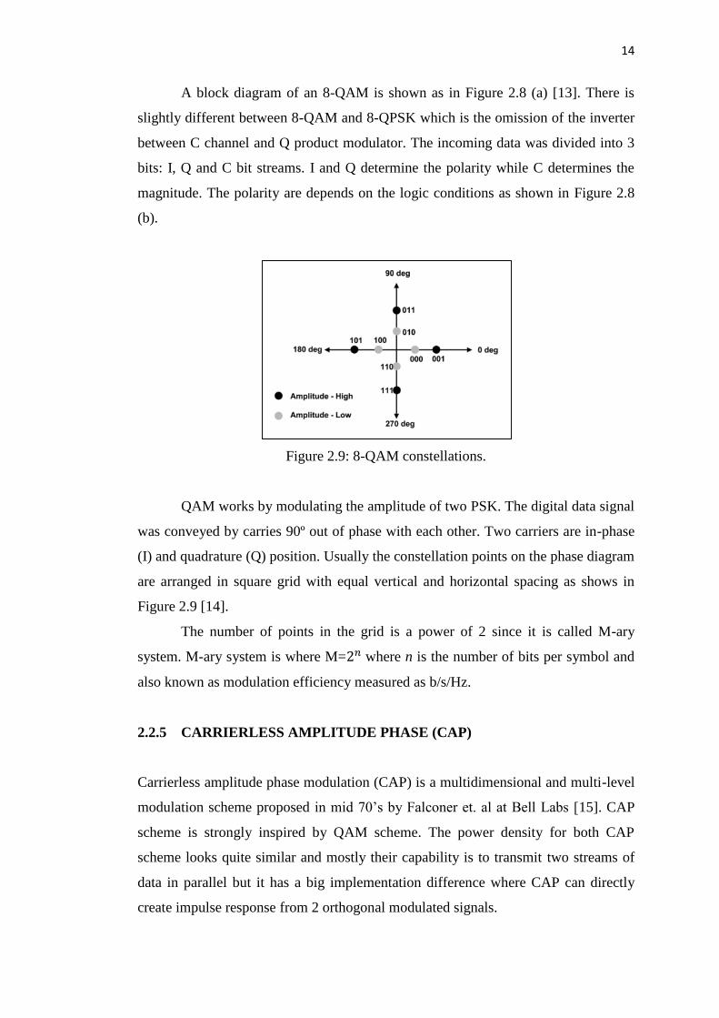
Figure 2.9: 8-QAM constellations.
QAM works by modulating the amplitude of two PSK. The digital data signal
was conveyed by carries 90º out of phase with each other. Two carriers are in-phase
(I) and quadrature (Q) position. Usually the constellation points on the phase diagram
are arranged in square grid with equal vertical and horizontal spacing as shows in
Figure 2.9 [14].
The number of points in the grid is a power of 2 since it is called M-ary
system. M-ary system is where M=2𝑛 where n is the number of bits per symbol and
also known as modulation efficiency measured as b/s/Hz.
2.2.5 CARRIERLESS AMPLITUDE PHASE (CAP)
Carrierless amplitude phase modulation (CAP) is a multidimensional and multi-level
modulation scheme proposed in mid 70’s by Falconer et. al at Bell Labs [15]. CAP
scheme is strongly inspired by QAM scheme. The power density for both CAP
scheme looks quite similar and mostly their capability is to transmit two streams of
data in parallel but it has a big implementation difference where CAP can directly
create impulse response from 2 orthogonal modulated signals.

15
Figure 2.10: Block diagram of CAP modulator
The block diagram of a digital CAP is shown in Figure 2.10 [16]. Firstly bit
stream is transmitted through a scrambler in order to randomize the data. The bit
clock is employed to synchronize the scrambler equals R that desired bit- rate. The
encoder block would accept block of m bits and generates symbol 𝑎𝑘 and 𝑏𝑘 per
symbol period. Then these 2 symbols assumed two dimensional displays which are
called a signal constellation as shown in Figure 2.11 [17]. Both symbols are fed into
digital shaping and the output will subtracted it through digital to analog converter
(DAC). Then it is followed by low pass filter (LPF).
Figure 2.11: 16 CAP constellations
CAP uses filters with orthogonal waveforms to differentiate data stream. It
means CAP does not depend on a carrier. That is why it is referred to as
‘carrierless’. It shows that CAP much simpler than QAM receiver but at the same
16
time still achieving the same spectral efficiency and performance. Basically CAP
scheme is used to reduce the complexity of the design. At the same time it was used
in order to minimize the cost of the equalizer at receiver.
2.3 FUNDAMENTAL OF FIELD PROGRAMMABLE GATE ARRAY(FPGA)
A Field Programmable Gate Array (FPGA) is an integrated circuit consisting of
interconnected blocks called Configurable Logic Blocks (CLB) [18]. There are two
popular languages to program FPGA, Verilog and VHDL.
FPGA is an integrated circuit and at the highest level, it reacts mostly like a
reprogrammable silicon chips. It used a grid of logic gates, similar to that an ordinary
gate array but the programming is done by the customer. The term “field-
programming” means the array is done outside the factory or in the field. There are a
few advantages offered by FPGAs which are cost effective, high performance, faster
time to market, shorter design cycles and true system delivery platform.
There are 3 main elements in FPGA which are logic blocks, input output
blocks and interconnection wire and switches. For input output blocks, it is more on
connecting to the pins of the package. The logic blocks are arranged in a two
dimensional array and the interconnection wires are organized as horizontal and
vertical routing channels between rows and columns of logic blocks [19, 20].
2.3.1 HARDWARE DESCRIPTION LANGUAGE
VHDL is stands for Very High Speed Integrated Circuits Hardware Description
Language. VHDL was developed in the early 1980s as a spin-off of a high speed
integrated circuit research project funded by the U.S Department of Defense [21].
VHDL become an IEEE standard in 1987 and it is updated in 1993.
With VHDL, user can describe the behavior of simple circuit building blocks
and then use these to build up the structure of a more complex circuit. Behavior
modeling is very useful because it allows the designer to build a logic circuit without
having to worry about the low level details. While structure modeling tells the
synthesis tools exactly how to construct a desired circuit.
17
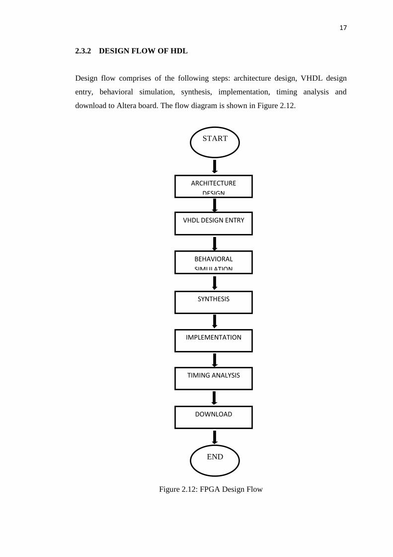
2.3.2 DESIGN FLOW OF HDL
Design flow comprises of the following steps: architecture design, VHDL design
entry, behavioral simulation, synthesis, implementation, timing analysis and
download to Altera board. The flow diagram is shown in Figure 2.12.
Figure 2.12: FPGA Design Flow
START
ARCHITECTURE
DESIGN
VHDL DESIGN ENTRY
BEHAVIORAL
SIMULATION
SYNTHESIS
IMPLEMENTATION
TIMING ANALYSIS
DOWNLOAD
END
18
In architecture design, it consists of project requirements. The output will be
describes the future device architecture, structural blocks, their function and
interface.
Second stage is VHDL design entry. This stage also known as declaration
stage. It will declare the device in a format HDL. Behavioral simulation is an
important stage where it wills checks HDL correctness by comparing output at HDL
model and the behavioral model.
The fourth stage is synthesis. It involves conversion of an HDL description to
a netlist. Synthesis is performed by special software called synthesizer. For a HDL
code that is correctly written and simulated, it should not be any problem. However,
it can reveal some problems and potential errors that cannot be found using
behavioral simulation.
A synthesizer generated netlist is mapped onto particular device’s internal
structure. The main phase of implementation stage is place and route or layout,
which allocates FPGA resources. Then these configuration data are written to a
special file by a program called bit stream generator.
Last stage covers timing analysis. During timing analysis, special software
will checks whether the implemented design satisfies timing constraints specified by
the user. When there is no error, all program will downloaded to an Altera board to
see the output.
2.3.3 ADVANTAGES OF USING HDL
HDL offers several advantages over traditional design methodology. In the next
subsection we will explain extensively the advantages of using HDL.
2.3.3.1 TOP DOWN APPROACH FOR LARGE PROJECTS
HDL is used to create complex designs. It is very useful for large and complicated
project. Once determined the design plan is done, designers can work independently
by divide it into several section of code.
19
2.4 OVERVIEW OF PREVIOUS WORK ON MODULATION
TECHNIQUE WITH FPGA
This subtopic summarized a set of published articles for peer- reviewed purposed.
These papers consists of highlighted methodology, analysis and also results of
modulation techniques using FPGA.
2.4.1 DESIGN AND SIMULATION OF FPGA BASED 16-QAM MAPPER
AND DEMAPPER USING VHDL.
Paper “Design and Simulation of FPGA Based 16-QAM Mapper and Demapper
Using VHDL” written by Chaw Su Nandar Hlaing was published in International
Journal of Science, engineering and Technology Research (IJSETR) July 2012.
The aim of this paper is to design the 16-QAM mapper and demapper using
VHDL. While Quartus II 7.2 was used to simulate the output, testing and
demonstration of the implementation design.
Figure 2.13: QAM transmitter block diagram.
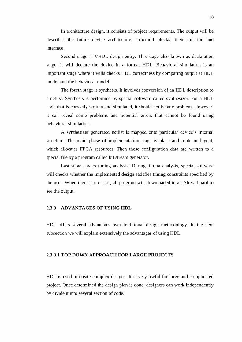
The design was divided into two parts which are QAM transmitter and QAM
receiver. Block diagram of transmitter was shown as in Figure 2.13 [22]. The block
diagram was consists of serial to parallel converter, temporary register, clock divider
and mapper. Random data was converted into 4 bits binary values by using serial to
20
parallel converter. It then was stored in the temporary register. Mapper takes the
values as an input and maps them into 8 bits signals of real and imaginary.
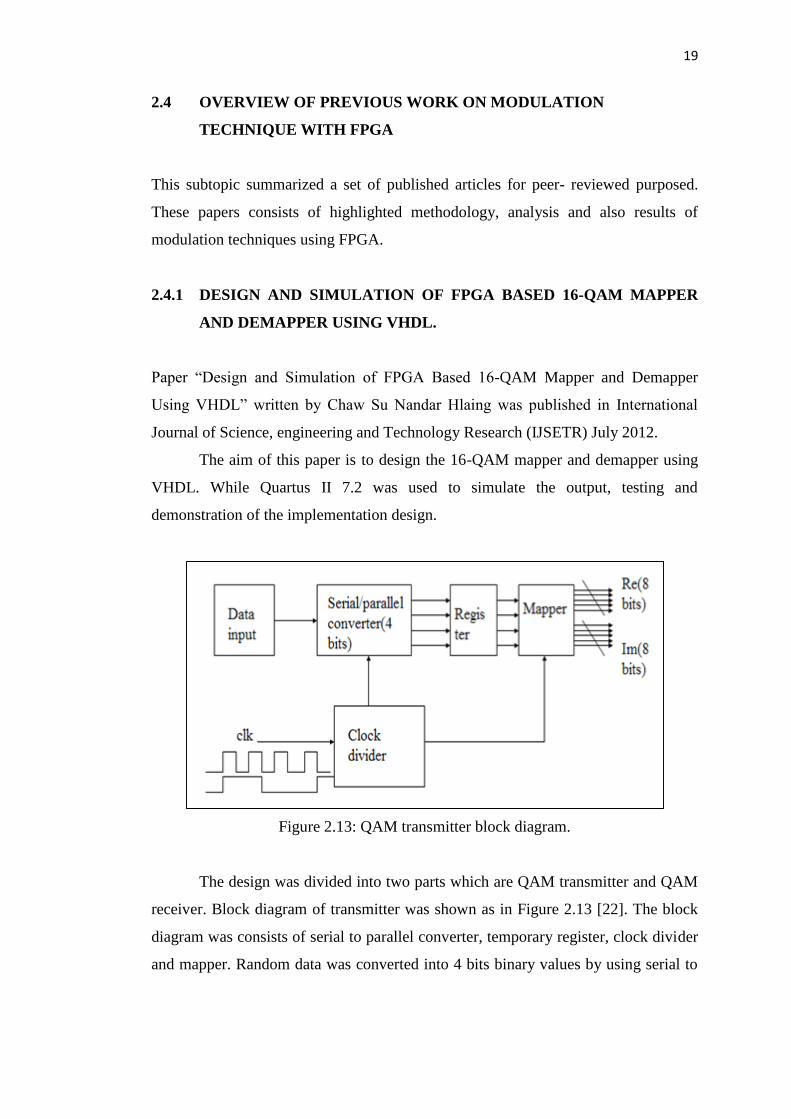
Figure 2.14: QAM receiver block diagram.
Figure 2.14 shows the block diagram of QAM receiver. 8 bits real and
imaginary from transmitter was demapper back into 4 bits binary and stored it in
temporary register. Then it turned into serial data at output once they passed through
parallel to serial converter.
Table 2.1 shows the 16 QAM system mapping. It consists of binary number
as input, numeric assign for mapper, digital assign real and imaginary number as
output.
Table 2.1: 16 QAM System Mapping
21
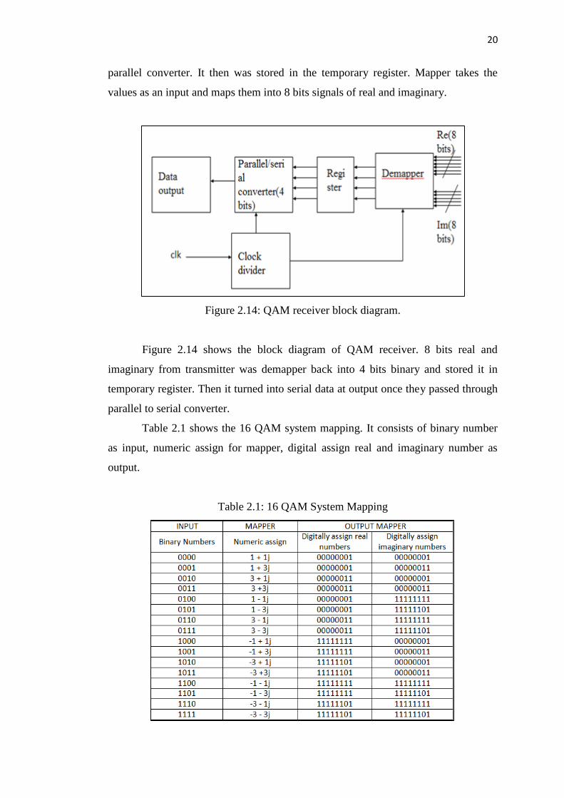
The result of this project, they manage to design the 16-QAM mapper and
demapper in VHDL source code. Simulation result in Quartus II as shown in Figure
2.15 shows a good agreement with 16-QAM mapping table.
Figure 2.15: Simulation of 16 QAM mapper and demapper in Quartus II.
2.4.2 LOW POWER QPSK MODULATOR ON FPGA
Paper “Low Power QPSK Modulator on FPGA” written by Prashant D. Tombare and
Ameed M. Shah was published in International Journal of Advanced Research in
Computer Science and Software Engineering in 2014.
This paper is proposed the implementation of FPGA kit using Active HDL
source code. They shifted signal starting from 45° to observe the output from
different phase of angle. Figure 2.16 showed the proposed block diagram of QPSK
modulator [23]. One ROM is used for carrier signal instead of two ROMs for sine
and cosine signal generator. The block diagram consists of a carrier source, phase
shifter, shift register, multiplexer and DAC.
22
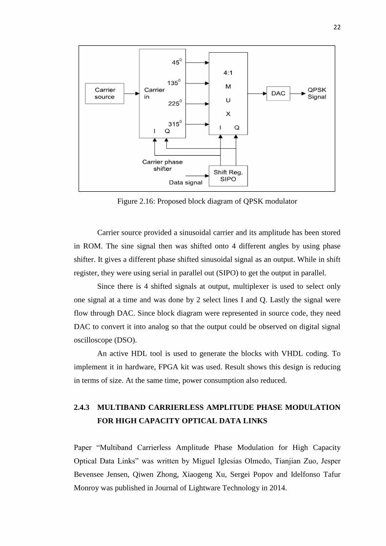
Figure 2.16: Proposed block diagram of QPSK modulator
Carrier source provided a sinusoidal carrier and its amplitude has been stored
in ROM. The sine signal then was shifted onto 4 different angles by using phase
shifter. It gives a different phase shifted sinusoidal signal as an output. While in shift
register, they were using serial in parallel out (SIPO) to get the output in parallel.
Since there is 4 shifted signals at output, multiplexer is used to select only
one signal at a time and was done by 2 select lines I and Q. Lastly the signal were
flow through DAC. Since block diagram were represented in source code, they need
DAC to convert it into analog so that the output could be observed on digital signal
oscilloscope (DSO).
An active HDL tool is used to generate the blocks with VHDL coding. To
implement it in hardware, FPGA kit was used. Result shows this design is reducing
in terms of size. At the same time, power consumption also reduced.
2.4.3 MULTIBAND CARRIERLESS AMPLITUDE PHASE MODULATION
FOR HIGH CAPACITY OPTICAL DATA LINKS
Paper “Multiband Carrierless Amplitude Phase Modulation for High Capacity
Optical Data Links” was written by Miguel Iglesias Olmedo, Tianjian Zuo, Jesper
Bevensee Jensen, Qiwen Zhong, Xiaogeng Xu, Sergei Popov and Idelfonso Tafur
Monroy was published in Journal of Lightware Technology in 2014.
23
The aim of this project is to investigate the spectral efficiency, tolerance
towards dispersion and bandwidth limitation of CAP in a novel multiband approach
(MultiCAP). The experiment was divided into two parts which is simulation setup
and experimental setup.
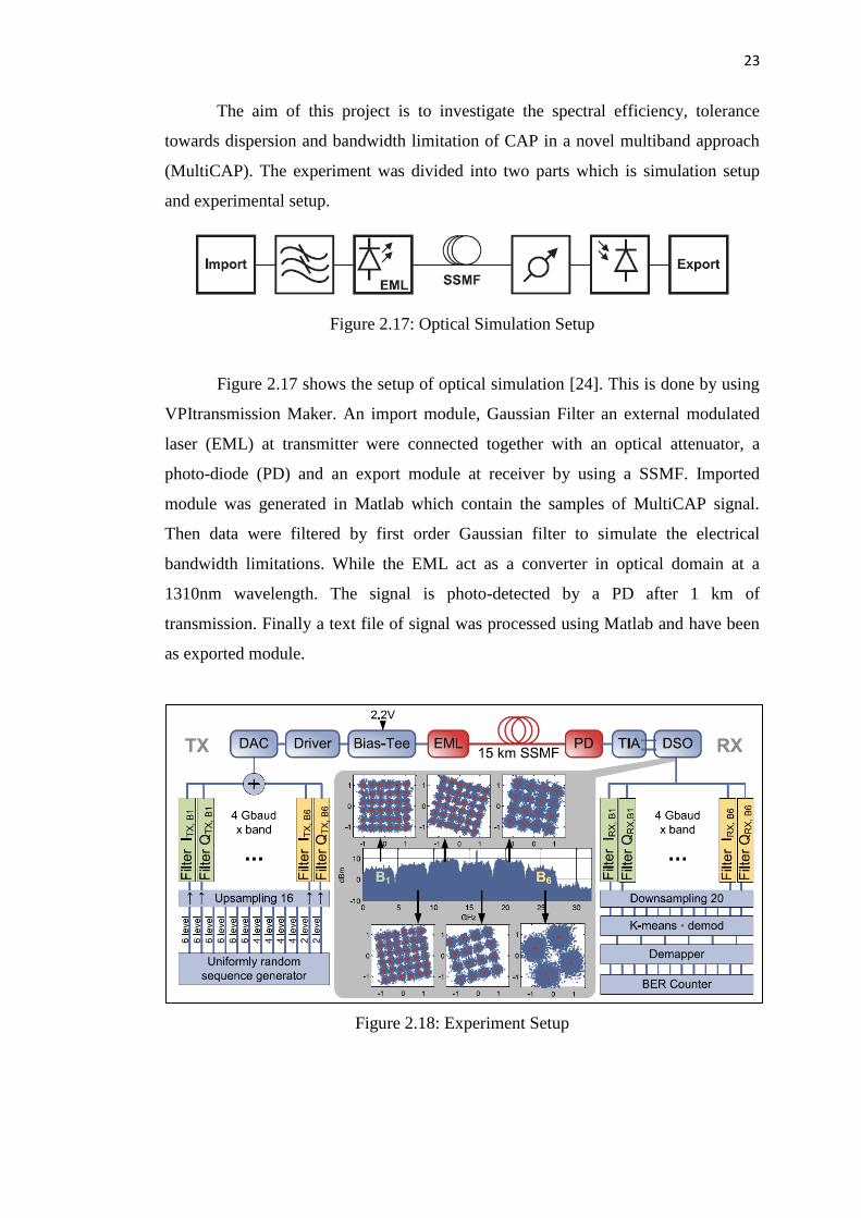
Figure 2.17: Optical Simulation Setup
Figure 2.17 shows the setup of optical simulation [24]. This is done by using
VPItransmission Maker. An import module, Gaussian Filter an external modulated
laser (EML) at transmitter were connected together with an optical attenuator, a
photo-diode (PD) and an export module at receiver by using a SSMF. Imported
module was generated in Matlab which contain the samples of MultiCAP signal.
Then data were filtered by first order Gaussian filter to simulate the electrical
bandwidth limitations. While the EML act as a converter in optical domain at a
1310nm wavelength. The signal is photo-detected by a PD after 1 km of
transmission. Finally a text file of signal was processed using Matlab and have been
as exported module.
Figure 2.18: Experiment Setup
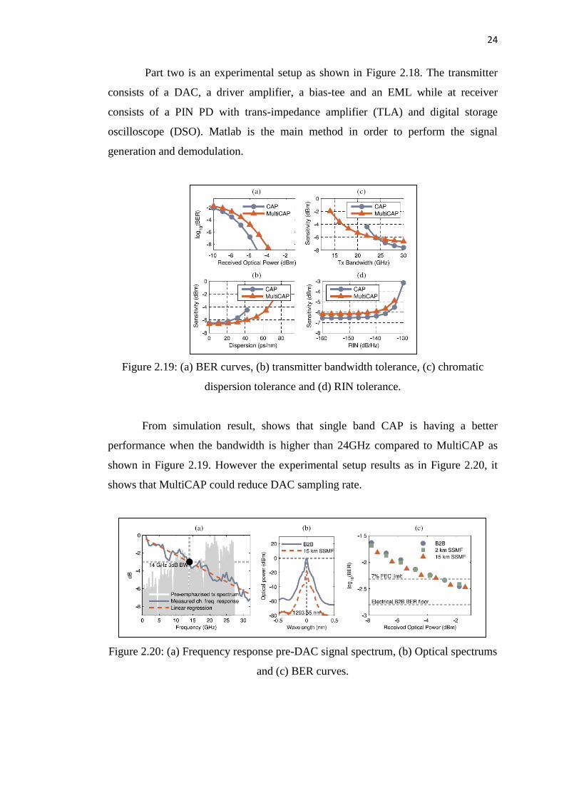
24
Part two is an experimental setup as shown in Figure 2.18. The transmitter
consists of a DAC, a driver amplifier, a bias-tee and an EML while at receiver
consists of a PIN PD with trans-impedance amplifier (TLA) and digital storage
oscilloscope (DSO). Matlab is the main method in order to perform the signal
generation and demodulation.
Figure 2.19: (a) BER curves, (b) transmitter bandwidth tolerance, (c) chromatic
dispersion tolerance and (d) RIN tolerance.
From simulation result, shows that single band CAP is having a better
performance when the bandwidth is higher than 24GHz compared to MultiCAP as
shown in Figure 2.19. However the experimental setup results as in Figure 2.20, it
shows that MultiCAP could reduce DAC sampling rate.
Figure 2.20: (a) Frequency response pre-DAC signal spectrum, (b) Optical spectrums
and (c) BER curves.
45
REFERENCES
1. Maurice Gagnaire, “Broadband Local Loops for High Speed Internet
Access”, Artech House, 2003.
2. Andrea Goldsmith, “Wireless Communication”, Cambridge University Press,
Aug 8, 2005.
3. A.K. Nigam, “Unit 3: Digital Modulation”, ITM University, Gurgaon, 2013.
4. S. Vijayachitra, “Communication Engineering”, Tata McGraw Hill
Education, 2013.
5. N. Vlajic, “Analog Transmission of Digital Data: ASK, FSK, PSK, QAM”,
CSE 3213, 2010.
6. Kwandwo Boateng and Charles Badu, “EE452 Senior Capstone Project:
Integration of Matlab Tools for DSP Code Generation”, Bradley University,
2006.
7. David Brandon and Jeff Keip, “Efficient FSK/PSK Modulator Uses
Multichannel DDS to Switch at Zero Crossings”, vol. 46, Jan 2012.
8. S.K Ibrahim, “High Speed Optical Communication Systems: Study of
Multilevel Modulation Formats”, VDM Verlag Publisher, 3rd July 2008.
9. Fang Ming Wu, Chun Ting Lin, Chia Chien Wei, Cheng Wei Chen, Hou Tzu
Huang and Chun Hung Ho, “1.1-Gb/s White LED Based Visible Light
Communication Employing Carrier-Less Amplitude and Phase Modulation”,
IEEE Photonics Technology Letters, Vol. 24, No. 19, Oct 1, 2012.
46
10. M. B. Othman, X. Zhang, L. Deng, J. Bevensee Jensen and I. Tafur Monroy,
“Experimental Demonstration of 3D / 4D-CAP Modulation Employing
CTCMA Channel Estimation”, Journal of Lightwave Technology, 2012.
11. J. R Smith, “Programming the PIC Microcontroller with MBasic”, Newnes,
2005.
12. A. Tarmo, “Introduction to Telecommunications Network Engineering”,
Artech House, 1 Jan 2003.
13. Mandeep, “ Chapter 2: Digital Modulation”, USM.
14. E. Ata, “Network Communications Technology”, Cengage Learning, 2011.
15. D. D. Falconer, “Carrierless AM/PM,” 1975.
16. G. Maurice, ”Broadband Local Loops for High-speed Internet Access”,
Artech House, 31 May 2002.
17. K. P. Keshab, N. Takao, “Digital Signal Processing for Multimedia
Systems”, CRC Press, 11 March 1999.
18. Henrik Bostrom, “An FPGA Implementation of a digital FM modulator”,
Linkopings Universitet, Sweeden, 9th June 2011.
19. Aseem Pandey, Shyam Ratan Agrawalla & Shrikant Manivannan, “VLSI
Implementation of OFDM”, Wipro Technologies, September 2002.
20. Nasreen Mev and Brig. R.M Khaire, “Implementation of OFDM Transmitter
and Receiver Using FPGA”, International Journal of Soft Computing and
Engineering (IJSCE), Volume -3, Issue-3, July 2013.
21. David Pellerin, “An Introduction to VHDL for synthesis and simulation”,
Accolade Design Automation.Inc, 1995.
22. S.N.H. Chaw, “Design and Simulation of FPGA Based 16-QAM Mapper and
Demapper Using VHDL”, published in International Journal of Science,
Engineering and Technology (IJSETR), vol. 1, issue 1, July 2012.
47
23. D.T Prashant and A.M. Shah, “Low Power QPSK Modulator on FPGA”, in
International Journal of Advanced Research in Computer Science and
Software Engineering, vol. 4, issue 1, January 2014..
24. M. I. Olmedo, T. Zuo, J. bevensee Jensen, Q. Zhong, X. Xu, S. Popov and
I.Tafur Monroy, “Multiband Carrierless Amplitude Phase Modulation for
High Capacity Optical Data Links”, published in Journal of Lightware
Technology, vol. 32, 2014.
25. R.H. Sharma and K.R. Bhatt, “A review on Implementation of QAM on
FPGA”, published in International Journal of Innovative Research in
Computer and Communication Engineering, vol. 3, issue 3, March 2015.
26. Maisara Othman, “High Dimensional Modulation MIMO Techniques for
Access Networks”, DTU Fotonik, Technical University of Denmark, 2012.
27. R. Ramaswami, K. Nsivarajan & G.H Sasaki, “Optical networks: A practical
perspective”, Morgan Kaufmann Publisher, 3rd Edition, 2009.
28. M. B. Othman, J. Bevensee Jensen, Xu Zhang, and I. Tafur Monroy,
“Performance Evaluation of Spectral Amplitude Codes for OCDMA PON,"
in (15th International Conference on Optical Net-work Design and Modeling
(ONDM), 2011.
29. Kris Gaj, “Sine/Cosine Using CORDIC Algorithm”, Gaurav Doshi.
30. J.B. Jesper, I.O. Miguel and T.M. Idelfonso, “Modulation Formats for
Beyond – 100Gbps Ethernet Optical Links – A Review of Research”, in Asia
Communications and Photonics Conference (ACP) 2013.
31. F. M. Gutierrez, “Implementation of a Tx/Rx OFDM System in a FPGA”,
Universitat Politecnica De Catalunya, 2009.


