

Executive Summary:
National Centre for Flexible Electronics (NCFlexE) came into existence formally on 14th
November, 2014 at Indian Institute of Technology Kanpur. The centre has been initiated
with an outlay of Rs. 133 crores sanctioned by the Department of Electronics and
Information Technology (DeitY), Government of India and support from IIT Kanpur. The
functioning of the centre will be coordinated by the executive committee headed by the
centre coordinator. The executive committee will operate under the guidance of a national
advisory committee (NAC) that has been set up under the chairmanship of the Director,
IIT Kanpur.
Due to the use of new materials and methods of manufacturing, flexible electronics
represents a break from the past and provides India with a fresh opportunity to become a
significant manufacturer of electronics. Centre’s objectives include development of a
national technology roadmap in coordination with other academic and industrial partners
in the country, establishment of a broad research program that leads to development of a
critical set of electronic components and partner with industry to develop prototypes and
commercialize the technology.
In the first year, NCFlexE has adopted a proactive strategy for publicity and branding to
reach out to the existing and potential industrial partners within and outside India. Three
‘roundtables’ to listen to the relevant industries for inputs, were held at Delhi, Bangalore
and Ahmedabad. A few industry workshops, press meets and other activities to raise
awareness among potential partners on flexible electronics and NCFlexE were organised
at IIT Kanpur. Centre has also actively participated in national and international level
interactions at industrial exhibitions and other events. Till December, 2015, seven calls
for the expression of interest (EOI) were floated for collaborative projects with the
industry. The areas targeted were – anticounterfieting, flexible photovoltaic technologies,
gas sensors, near-field communication tags, OLED for lighting and displays, printable inks
and printed batteries.
In the first year, five companies have signed up for the partnership with NCFlexE with
more than Rs. 1 crore funds for the projects. A project approval mechanism has been put
in place at the centre to approve and monitor proposals for the development and
prototyping activities. Each project is encouraged to involve at least one partner industry.
The proposals are peer reviewed by experts from around the country. Based on the peer
review, a sub-committee setup by the NAC Chairman, approves them.
The building construction and equipment purchase for the centre are on track. In the first
year, after institute space committee approval, building plan approval and construction
tendering, construction started in May 2015 and by the end of the year, the roof of the
ground floor is constructed. The equipment needed for successfully running the centre are
being procured in a systematic matter.
Having started the journey on a firm footing in the first year of its existence, NCFlexE
looks forward to the coming years to grow into an international centre of excellence to
help establish a flexible electronics ecosystem in India.
Table of Content
I Branding & Publicity Activities ......................................................................................................... 6
Industry Membership & Project Approvals: ............................................................................................. 7
Branding and Publicity Activities up to March 2016 ............................................................................... 8
II NCFlexE Projects ................................................................................................................................ 9
PAM Approved Projects ........................................................................................................................... 9
Brand Protection Labels: Phase I: Contact-based Tax Stamp Tags ...................................................... 9
Prototype WOLED based lighting tiles ................................................................................................ 9
Breast cap for detection of breast cancer ............................................................................................ 10
Technology Development for Commercialization of Low Cost Anti-counterfeiting Tags ................ 10
Projects related to EOIs .......................................................................................................................... 11
Synthesis, characterization and formulation of conductive silver nanoparticle (NP) ink for
inkjet printing ...................................................................................................................................... 11
Printed Organic Solar Cells on Flexible Substrate ............................................................................. 11
Flexible sensors .................................................................................................................................. 12
Printed Batteries .................................................................................................................................. 13
Development of Organic Diode Array for Temperature Sensing ....................................................... 14
Development of dielectric inks for printing ........................................................................................ 15
Development of TFT backplane for QVGA flexible AMOLED displays .......................................... 15
Flexible white OLED for lighting and display ................................................................................... 16
III NCFlexE Infrastructure and Manpower .................................................................................... 17
Manpower hiring: ................................................................................................................................... 17
Building: ................................................................................................................................................. 17
Equipment purchase: .............................................................................................................................. 18
IV FUNDED PROJECTS .................................................................................................................. 20
List of Other Projects .............................................................................................................................. 20
V PERSONNEL .................................................................................................................................... 21
Core Faculty @ SCDT .............................................................................................................................. 21
Core NCFlexE Members .......................................................................................................................... 22
VI COMPLETED THESES .............................................................................................................. 24
Ph.D. Theses ............................................................................................................................................ 24
M. Tech. Theses ...................................................................................................................................... 24
VII PUBLICATIONS .......................................................................................................................... 27

Journal Articles ....................................................................................................................................... 27
Conference Proceedings ......................................................................................................................... 29
VIII PATENTS ...................................................................................................................................... 31
IX AWARDS ....................................................................................................................................... 31
I Branding & Publicity Activities
In its first year, NCFlexE activities for branding and publicity included the following
- Personal Networking and References (Corporations, Centres in this field etc.)
- Industry Associations – IESA, ELCINA, AIMED, IPCA, Smart Card
Manufacturers Association, ACMA, FICCI, CII etc.
- Events organized in conjunction with CII, AIMED etc. (Table I)
- Industry Workshops (Table I)
- Sector Wise Roundtables in various cities – Healthcare, Packaging and Printing
etc.
- Govt. organizations – DBT, DST, GITA, CII, etc.
- Attending Workshops and Conferences in relevant areas (Table II)
Table I. Exhibitions and Events – Organized by NCFlexE
Event Date Venue Outcome
Launch and Laying of the
Foundation stone (as part of
Digital India Launch)
1st July, 2015 IIT Kanpur Publicity and awareness
created
Short course on Flexible
Electronics
6-11 July, 2015 IIT Kanpur Awareness & human
resource development
Workshop on Flexible
Electronics
10th July, 2015 IIT Kanpur Publicity and awareness
Roundtable for sensors 22nd September
2015,
New Delhi Awareness created.
Preliminary leads obtained
FLEXE 2015, Industry
Workshop
12th October,
2015
IIT Kanpur Identified several
companies for second
stage discussions
Roundtable - Healthcare 8th December,
2015,
Bangalore Identified potential
partners for Healthcare
and Diagnostics
Roundtable- Flexible
electronics for Healthcare and
packaging
29th January,
2016
Ahmedabad Identified potential
partners for Healthcare
and Diagnostics
Table II. Exhibitions and Events – Attended by NCFlexE
Event Date Venue Outcome
TAITRONICS 6th-9th October,
2015,
Taipei,
Taiwan
Awareness created. Preliminary leads
obtained
AIMED
Roundtable
6th November
2015, New Delhi
New Delhi Contacts established with Medical
Equipment makers
Indo Japan CWG 30th November,
2015
New Delhi Invited Japanese academic and industry
players for possible collaboration
PAMEX 2015 9th-12th
December,
Mumbai Awareness for printing industry
IESA –VS 2016 3-4 February,
2016 at
Bangalore Contacts established with PCB and
Semiconductors manufacturers
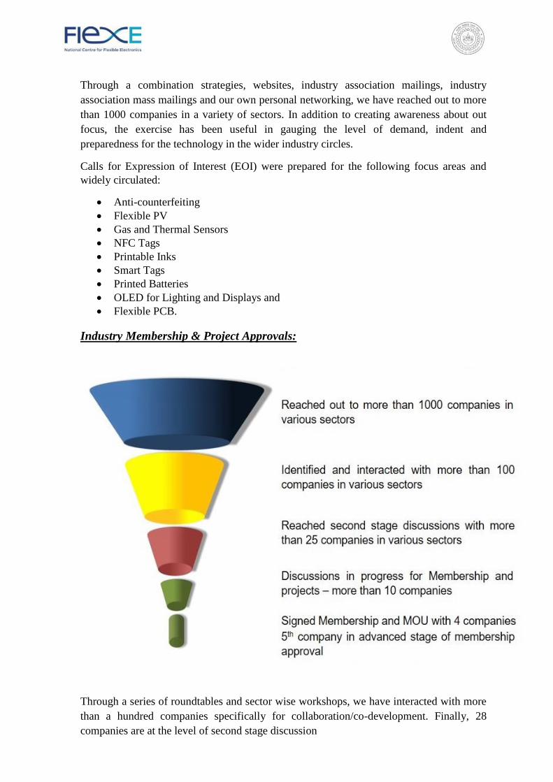
Through a combination strategies, websites, industry association mailings, industry
association mass mailings and our own personal networking, we have reached out to more
than 1000 companies in a variety of sectors. In addition to creating awareness about out
focus, the exercise has been useful in gauging the level of demand, indent and
preparedness for the technology in the wider industry circles.
Calls for Expression of Interest (EOI) were prepared for the following focus areas and
widely circulated:
Anti-counterfeiting
Flexible PV
Gas and Thermal Sensors
NFC Tags
Printable Inks
Smart Tags
Printed Batteries
OLED for Lighting and Displays and
Flexible PCB.
Industry Membership & Project Approvals:
Through a series of roundtables and sector wise workshops, we have interacted with more
than a hundred companies specifically for collaboration/co-development. Finally, 28
companies are at the level of second stage discussion

Out of these efforts, we have FIVE Industry members this year (Table III) that have signed
the NDA cum membership document with NCFlexE this year. Projects proposals with
three of them have been written. As per the decided mechanism for project approval
(Annexure 2: Project Approval and Monitoring procedure), the proposals were sent for
external peer review and at least two appraisals for each proposal were obtained. Project
Approval and Monitoring (PAM) Committee met on 13th Oct 2015.
Table III. Industry Partners and Project Approval Status
Sl.
No
Item Activities Status
1 Manipal
Technologies
Security Tags for Packaging Project approved. Ready for
Industry membership. MOU for
project to be signed.
2 Chain
Electronics
Seven segment OLED and
flexible PCB
Membership signed. Project
proposal in progress.
3 Applied
Materials
Processing equipment NDA and Membership agreement
signed.
4 Murata
Manufacturing*
Flexible sensors for breast
cap
NDA signed. MOU under review
for signature.
The total funds committed by these partners in the first year has crossed Rs. 1 Cr.
* Advanced stage of approval of membership.
Branding and Publicity Activities up to March 2016
Table IV. Exhibitions and Events – To be organized by NCFlexE
Roundtable – Packaging, Pharma, PV
and OLED
4th March, 2016 Mumbai/Pune
Roundtable – Healthcare and Medical
Equipment
28th March, 2016 Bangalore/Hyderabad
II NCFlexE Projects
PAM Approved Projects
Brand Protection Labels: Phase I: Contact-based Tax Stamp Tags
Product counterfeiting is a thriving multi-billion dollar global industry and hurt many of
the brands and products badly. There are many anti-counterfeiting solutions available but
either they are not cost effective or can be easily copied. Thus the development of a
printed electronic version of anti-counterfeiting device which offers good anti-
counterfeiting protection while being cost efficient would be attractive to businesses
whose valuable brands or evasion of taxes are constantly challenged.
The basic aim of this project is to address the need of developing anti-counterfeiting
features for protection against spurious products. Another advantage of this development
is towards upgradation of the technology for creating a niche in the market (taking a
strategic lead over competitors). In this genre, this project specifically intends to develop
an additional electronic security feature solution for Tax Stamp labels. The label should
empower the Tax inspector to verify a unique identity by reading the label pasted on the
product using a contact electronic reader. Being a large volume application, it needs to be
manufactured (printed) at a high speed (so that it can be integrated into existing lines for
tax stamp) within acceptable limits of additional cost.
In Phase-I, we are targeting development of tags based on contact reading as an example
of a generic effort towards in expensive tags.
Prototype WOLED based lighting tiles
In India, 16% of the total generated electrical power is consumed for lighting. Still 25-
30% of the total population of India lives without access of electricity (approximate 400
million) and largely depend on the kerosene oil for lighting. Considering the fact that the
present lighting devices have low efficiency (5-20%) and environmental hazards (contain
mercury), there is great potential for substantial energy saving as well as environmental
prtection (by reducing green house gases emission) by switching to more energy efficient
and eco-friendly lighting devices.
Alternative SSL technologies exist that have the potential to compete with the inorganic
white LEDs in the future. These are called white organic light emitting diodes (WOLEDs)
and white polymer light emitting diodes (WPLEDs). WOLED is the only technology that
can create large "area" lighting panels (as opposed to point or line lighting enabled by
LEDs and Fluorescent bulbs). These OLED devices are made by amorphous polymers
semiconductors that can be deposited on large area, flexible and lightweight substrates and
offer significant advantages as polymers can be directly processed from solution by spin
coating, ink-jet printing, and blade coating. WPLEDs can be made using roll-to-roll
printing process with high throughput which reduces the cost of the lighting panels further
for general lighting application. OLEDs can be used to
make flexible and transparent panels, and can also be color-tunable. OLEDs emit soft

diffused light - in fact OLED lighting is the closest light source to natural light (with the
exception of the old incandescent lamps).
The objective is to develop prototype WOLED lighting tile on glass that can be arranged
to make flexible luminaires. In the second phase, the technology will be transferred to
flexible substrates.
Breast cap for detection of breast cancer
It is reported that by 2020, 70% of the world’s cancer cases will be in developing
countries, with a fifth being in India. The previous year, the Indian Council of
Medical Research provided an analysis of cancer cases among women in various cities
- Delhi, Mumbai, Chennai, and Bangalore from 1982 to 2005, showing that until about
10 years ago, 10 per 100 000 women got breast cancer, compared with 23 per 100 000
now; and by 2020, breast cancer is set to overtake cervical cancer as the most common
type of cancer among all women in India
There is a need for early detection of the disease for facilitating effective
remedial measures. This has been highlighted in a recent case study conducted in India
which found that women in developing countries survive roughly 10 years shorter after a
breast cancer diagnosis compared to women in developed countries, and a reason for this
among others is late detection. A vast population not having an easy access to the
diagnostic centers, due to the prohibitive costs and to the locational issues, adds to the
burden of the disease in India. According to a 2008 WHO report, there is one doctor
for every 10,000 Indians. Moreover, in cities, 80% of India’s medical staff works in the
private sector.
The objective of the work is to develop a low-cost breast cap using flexible temperature
systems capable of providing the skin temperature mapping of the breast to be analyzed
using algorithms for detecting abnormalities attributed to breast cancer. A successful
technology could help make breast cancer diagnosis accessible and affordable.
Technology Development for Commercialization of Low Cost Anti-
counterfeiting Tags
Counterfeiting is a continuously increasing problem, especially in the developing
world. In one case, counterfeit books, CDs, electronic equipment, or consumer
durables in general are available which impacts the business conditions in the country.
The other case is even more serious, which involves fakes in foods and
pharmaceuticals, creating an additional health risk. So manufacturer, producer and even
end users want a high level of security to protect their products. The World
Customs Organization reported that approximately 6% of global goods are fake. In
many cases, it is very difficult to identify counterfeit goods from genuine ones.
We are identifying counterfeiting of medicines as the most severe risk, hence focus of this
work would be on development of anti-counterfeiting strategies in general and
for medicine packages in particular.

Objectives
To develop and demonstrate a physical method of printing on a package that
(a) has potential to prevent or severely mitigate counterfeiting of the packages (not the
contents inside),
(b) offers verifiability in the hands of consumer without a need to carry an extra
detector or access to communication networks,
(c) Is produced with bill of materials below Rs. 1 per tag.
Projects related to EOIs
Synthesis, characterization and formulation of conductive silver nanoparticle
(NP) ink for inkjet printing
A tremendous interest in printable electronics has been developed in the last decade which
is also evident in the literature. Printed electronics refers to the fabrication of electronic
circuits and devices using printing process, especially on flexible substrate.
Conventionally, manufacturing of electronic devices can only be realized by expensive
multistage processes such as photolithography, vacuum deposition, and electro less
plating. These processes are not eco‐friendly and create mostly toxic and hazardous
chemicals. The motivation behind the printed electronic is to create large scale
manufacturing of electronic devices in a faster and cheaper way. Inkjet printing is very
attractive method for manufacturing organic solar cell electrode, RFID tags, OTFT,
flexible LEDs and displays. Inkjet printing is favorable for automation and enables
patterning with high resolution line and space dimensions can be small as 20 micron. Due
to the complex nature and very challenging requirements for inkjet inks, preparation of
such inks is often very complicated. The ink must meet out the physicochemical
requirement of print head such as viscosity and surface tension.
Objectives
a) Development of methodology for making stable conductive metal nanoparticles
(Ag/Au/Cu).
b) Ink formulation of conductive inks using suitable solvent preferably eco‐friendly
solvent
c) Process development for inkjet printing and sintering.
d) Performance development of the printability over flexible substrates like
paper/PET/PEN/PI using inkjet printer.
e) Development of business plan for the low cost conductive inks as a commercial product
Printed Organic Solar Cells on Flexible Substrate
Organic solar cells use organic semiconductors for the active layer of the solar cells. They
have the potential to be manufactured on a large scale at low cost per unit. With proper

product development, the fabrication process and the products developed may be
ecologically friendly. Moreover, their fabrication on flexible substrate such as appropriate
plastics or paper can help implement solar modules that are lightweight, can be conformal
to the structure on which they are mounted and may be folded or rolled up for ease of
storage and transportation.
In this project, we will be building organic solar cells on flexible substrates such as paper
or plastic (PET) by the printing techniques. Some of the main challenges in this project
will be developing a printing process and the inks needed for that to build the solar cell; to
design the sub-modules and test them effectively for efficiency and stability; and to build a
stable process line so as to fabricate sub-modules of size 10 cm × 10 cm or more that have
efficiencies above 3% which last for at least six months.
Objectives
The primary objective would be to develop a printing technology that will allow us
to print an organic solar cell sub-module onto a flexible substrate such as paper or
plastic.
Another objective would be to develop sub-modules of size at least 10 cm x 10 cm
on a substrate size of 15 cm x 15 cm and integrate them with chips / circuits that
will help charge a battery or deliver power to any suitable and practical electrical
load.
Another objective would be to work with industry partners to integrate the sub-
module of appropriate size on a system to form a commercial product.
Flexible sensors
(i) Sensors for detection of heavy metals in water
Providing clean drinking water to the population has become an increasing challenge with
depletion of water sources and pollution of water bodies. The pollutants in the water can
be broadly classified as metals, organics and pathogens with a large variety of species in
each of these classes and the pollutant profile could be area specific. The types and
concentrations of these pollutants have increased, all leading to serious health
consequences. There is a need for monitoring the quality of the water at all stages, from
the source till the end user. The goal of the proposed activity is to develop low-cost
chemical sensors for detecting pollutants in drinking water. The market for these sensors
not only includes the general populace, but also the regulatory agencies and the water
purification industry. Initial focus would be on detection of heavy metal (e.g. cadmium,
chromium, manganese, arsenic) ions.
Objectives
1. Generate the knowledge, by formulating and executing pertinent research
problems, as provided in the proposed work modules, needed to design and
fabricate a sensor for detecting heavy metal ion pollutants in water
2. Setting up of the design specifications for the FlexE team to develop the device.

(ii) Breathalyzer for non-invasive disease diagnostics
Exhaled breath while primarily comprises nitrogen, oxygen, carbon dioxide and water
vapor (75%, 16%, 4%, and 4% by volume, respectively), also contains trace levels of other
gases which can be markers of the disease status. For example, acetone could indicate
diabetes, ammonia could indicate kidney problems, toluene could indicate lung cancer.
The use of breath analysis is a promising field for non-invasive detection. However, the
breath analysis poses significant challenges to specifically identify components at low
detection limits.
Objectives
1. Generate the knowledge, by formulating and executing pertinent research
problems, as provided in the proposed work modules, needed to design and
fabricate a breathalyzer.
2. Setting up of the design specifications for the FlexE team to develop the device.
(iii)Disease diagnostics from body fluids
Biomarkers present in body fluids (blood, saliva, urine) can indicate the pathological
condition of the body. For example: blood urea nitrogen (BUN) and creatinine are
biomarkers for impaired renal function, levels of the prostate specific antigen are
biomarkers for prostate cancer. Detection of disease biomarkers in the fluids can be
utilized for early disease detection. Also, these can be used to monitor the response to
therapies.
Utilization of microfluidics based platforms has the potential of rapid and low-cost
detection techniques with point-of-care applications, which could be very relevant to the
Indian context.
Objectives
1. Generate the knowledge, by formulating and executing pertinent research
problems, as provided in the proposed work modules, needed to design and
fabricate a microfluidic sensor array.
2. Setting up of the design specifications for the FlexE team to develop the device.
Printed Batteries
Every electric device needs to be powered. Low-cost, wearable, flexible electronics e.g. in
the form of smart watches, sensors embedded in clothing, activity trackers, and health-
monitoring tags are anticipated to be widely adopted. Future generations of these devices
would be thin, conformable to the human body, ubiquitous, and almost imperceptible to
the user. Powering these devices while retaining their mechanical properties will be a
challenge.
Batteries are essential for powering portable electronic devices. A battery is a closed
system in which energy is stored in chemical form, and it is converted to electrical energy
by connecting the battery to an external load to complete the circuit, causing electric
current to flow between the anode and cathode.

The standard batteries (coin cells, can cells etc.) are bulky and do not provide
the flexibility in shape and design required by new printed electronics. By printing the
battery itself too, all advantages of the printed, flexible electronics can be utilized.
An electrochemical cell consists of active layers supported on conductive substrates
(current collectors) to form the anode and cathode of the battery. The electrolyte provides
ionic contact between the electrodes and helps to complete the redox reactions within the
cell. Printing processes such as screen, stencil, and blade printing are well established and
they can be used to deposit battery components by designing printable inks for the active
layers, current collectors, and electrolyte. Batteries fabricated using printing processes
have the advantage of low cost, flexible form factor, ease of production, and integration
with electronic devices. The term “printed battery” is used to describe a battery for which
at least one of the components is solution processed and deposited using a printer.
Objectives
development of printed batteries
development of free – form batteries / printed on demand
development of disposable batteries
Development of Organic Diode Array for Temperature Sensing
Temperature is a fundamental physical parameter that needs to be measured for a wide
range of applications. Low cost temperature sensor arrays are required for applications
ranging from electronic skin, biomedical thermal imaging, and structural temperature
monitoring. Organic electronics offers the prospect of high density of sensors through
monolithic fabrication on flexible and cheap plastic substrates. There are a number of
ways of realizing a temperature sensor using organic materials including resistors,
transistors etc. Resistors have the advantage of being simple but in an array their
density is limited by the requirement of direct addressing where each sensor has its
own individual set of external terminals. Transistor based temperature sensors can be
used to fabricate an active matrix type large sensor array but they are more
complicated to fabricate and are likely to be expensive as well. Although, Silicon
Diodes are widely used for sensing temperature, there are very limited reports of use of
organic diodes for this purpose. Diodes offer the prospect of building a fairly large
array of sensors through passive addressing scheme and represent a solution that is
intermediate between simple direct addressed resistive array and complicated transistor
based active matrix array. The aim of this research proposal is to develop a sensitive
and reliable organic semiconductor based diode temperature sensor and a proof-of-
concept 3 x 3 passive matrix array.
Objectives
1. Development of an organic diode based temperature sensor in the range 0-50 oC on
glass substrate using spin coating/vacuum deposition techniques
2. Development of proof-of-concept 3 x 3 sensor array with associated external
readout electronics
3. Development of a of fully inkjet printed diode and its evaluation as a
temperature sensor
Development of dielectric inks for printing
The proposal is aimed at developing dielectric inks for various printing processes and wide
range of applications such as printed TFTs, RC component in smart tags and as printed
insulators in flexible circuits.
This project will investigate various polymer dielectrics properties and their ink properties
with different solvents for printing applications. Phase I of the project will aim at
developing polymer dielectric inks of different properties as per specific application and
printing process. In phase II, nanostructure – polymer composite dielectric inks will be
developed for enhanced properties.
Dielectric inks development will be in-line with specifications of various components
under development at FlexE (such as printed TFTs) and prototypes (such as RC circuits in
smart-tags).
Objectives
Dielectric inks are integral component of printed and flexible electronics. Development of
dielectric inks would be in two phases
Objectives of Phase – I
i. Processing of polymer dielectric inks with different solvents
ii. Study repeatability, and stability of the inks using MIM structures.
iii. Rheological study of inks and formulation as per printing process specifications.
iv. Ink-jet printable dielectric inks with specifications as per application(s).
Objectives of Phase – II
i. Study of dielectric properties of nanoparticle – polymer composites.
ii. Stability and repeatability of composite dielectric inks.
iii. Ink formulation for different printing processes (such as ink-jet, screen, slot-die
etc.)
iv. Tuning of dielectric properties of ink as per application(s).
Beyond the 2-year period (October 2017), ink properties will be continuously upgraded to
follow a roadmap based on internal requirements and international standards.
Development of TFT backplane for QVGA flexible AMOLED displays
Indian market for hand-held display devices is poised for a steep growth. Currently
smartphone user penetration is only at 17% of Indian population, in contrast to > 40% in
China. Even if a small fraction of hand-held devices go flexible, overall volume for such
devices in India will be huge. In absence of a technology know-how in this field, chances
of indigenous manufacturing of flexible display devices are very meagre. Absence of
technology and skilled manpower will also act as a barrier for foreign industries to
manufacture in India. Furthermore, various technology components developed in the
course of this project, i.e. flexible TFT backplane, flexible thin film encapsulation (TFE),

top emission OLED, substrate handling solutions, and process integration can be
disseminated to the manufacturing of other flexible electronics devices, such as TFT
technology for circuits and backplane for sensors, memories, imager etc. and TFE for any
flexible electronics device susceptible to moisture. Therefore, this project will serve as a
foundation to many other flexible electronics applications.
In this project we will develop a flexible AMOLED display fabricated on a polymer
substrate with metal-oxide TFT backplane and OLED frontplane technology. The project
involves bringing together technology groups mainly involved in TFT arrays, barriers and
encapsulation, and OLED development in order to achieve a monolithic integration of
backplane and frontplane on a polymer substrate. Driver IC integration and flexbonding
expertise will be inherited from the passive matrix OLED display project earlier executed
by SCDT.
Objectives:
Flexible AMOLED display is a technology integration project involving various
components being developed in the FlexE Centre. This project will serve to following
objectives:
1. Development of metal-oxide TFT backplane technology
2. Development of top-emission OLED frontplane technology
3. Developing thin film barrier and encapsulation
4. Developing flexible substrate handling solution (bonding/debonding)
5. Display driving infrastructure
Flexible white OLED for lighting and display
The traditional sources of lighting are incandescent bulbs and florescent tubes with
luminous efficiency of 15 lm/W and 90 lm/W, respectively. Solid state lighting is
considered the next generation lighting technology because of its improved efficiency and
life-time, but technological breakthrough is required to reduce its cost. There are two
approaches – inorganic LEDs (GaN based) and white organic LEDs (WOLEDs).
Inorganic LEDs have a definite advantage of high efficiency (at device level), and life
time, but they are still very costly when one compares the equivalent luminaire cost
(INR/kLm) of lighting. This is why WOLED is considered a good alternative, but
considerable improvement of efficiency, lifetime, and cost is required. Internationally, EU
(EUROPE), DOE (USA) and Japan are funding several OLED lighting projects. There
have been few commercial products, by Osram and Philips, introduced at efficiency less
than 20Lm /W, although the highest efficiency reported is >100 Lm/W.
R&D on WOLED at Flex-E center will continuously work on the following aspects:
1. WOLED stack (for evaporation and for solution processed devices) with two
objectives: maximize device efficiency and minimize the cost of substrates,
coatings, organic compounds
2. Light extraction techniques
3. New device structures: transparent WOLED for building integrated lighting

There will be efforts to find possible products along the way and to improve
manufacturability of WOLED for commercialization.
There will be WOLED sub-teams in the Flex-E center to (i) reduce the BOM, (ii) improve
OLED stack for thermal evaporation on flexible substrate, (iii) improve OLED stack for
printing techniques, (iv) increase light extraction (v) develop encapsulation to enhance
life-time, (vi) design novel products.
III NCFlexE Infrastructure and Manpower
Manpower hiring:
Substantial progress has been made in the area of team building. The COO joined the
centre in May, 2015. Three team leaders (RE) have already joined the team and started
contributing significantly to the development activities. More candidates have been
identified and interviewed to fill the remaining positions. Project staffing is also well
under way. In summary, about 60% staffing is now complete.
Building:
The ground clearing work started in May, 2015. During excavation, there were several
challenges faced related to underground cables which were diverted before excavation
could proceed. Since then, work progresses rapidly and the plinth level Foundation work
has now been completed. The sequence of photographs below shows the development of
the construction of the building. Construction is on schedule and target completion is by
Dec 2016.

Equipment purchase:
The equipment list was divided into 2 phases based on immediate requirements as well as
the space availability. Some of the equipment, which are large in size and needed at a later
stage, were moved into Phase II category (to be in line with the completion of the new
clean room in the new building).
Summary: First phase Equipment defined and orders being placed.

Academic Report
2015-2016

IV FUNDED PROJECTS
List of Other Projects
Sl.
No.
Project Name Funding
Agency
Amount
(Rs. In
Lakhs)
Duratio
n
Project
Investigator
01 Design and Development of of
Organic Solar Cell sub-Modules
MNRE 663.52 2011-
2015
Dr. S.S.K. Iyer
02 Research and Development of
InGaZnO4 (IGZO) Large Area
Electronics and its Application to
Active Matrix Flat Panel Display
DST 686.95 2011-
2014
Dr. Deepak
Gupta
03 Organic/ Polymer Light Emitting
Diodes Fabrication and
Characterization
DRDO 10.00 2012-
2014
Dr. Y.N.
Mohapatra
Dr. Ashish
04 Stand –off detection of explosives
based on immunochemical
Techniques
Office of
the
Principal
Scientific
Advisor
Governm
ent of
India
567.00 2011-
2014
Dr. Siddarth
Panda
05 Flexible Printed Integrated
Disposable Electronics
(FLEXIPRIDE)
Indo-
German
Science &
Technolo
gy Centre
107.25 2012-
2015
Dr. Y.N.
Mohapatra
Dr. B. Mazhari
V PERSONNEL
Core Faculty @ SCDT
Sl
No
Name Department Designation
01 Dr. Deepak Gupta MSE, SCDT Professor
02 Dr. Y.N.Mohapatra Physics, SCDT Professor
03 Dr. B.Mazhari EE, SCDT Professor
04 Dr. Monica Katiyar MSE, SCDT Professor
05 Dr. S.Sundar Kumar Iyer EE, SCDT Professor
06 Dr. Siddhartha Panda CHE, SCDT Professor
07 Dr. Anshu Gaur MSE, SCDT Assistant Professor
Deepak Gupta Professor, Materials Science and Engineering Experience Ph.D., Materials Science and Engineering, UC Berkeley, 1993 Argonne National Laboratory, Motorola, IIT Kanpur Research Interest Organic Semiconductors, Displays, Electronic and Optical Materials
Y. N. Mohapatra Professor, Physics and Materials Science Programme Experience Ph.D., IISc, 1988 IIT Kanpur Research Interest Semiconductors, electronic and photonic , materials, OLED/PLED
Baquer Mazhari Professor, Electrical Engineering Experience Ph.D., Electrical Engineering, U. Illinois, Urbana-Champaign, 1993 Research Interest Organic Semiconductors, Semiconductor device modelling and analog circuits
Monica Katiyar Professor, Materials Science and Engineering Experience Ph.D., Materials Science and Engineering, U. Illinois, Urbana-Champaign, 1994, Motorola, IIT Kanpur Research Interest Organic Electronics(OLED/OTFT),Printable Electronics Thin Films, Material Characterization
S. Sundar Kumar Iyer Professor, Electrical Engineering Experience Ph.D., Electrical Engineering, UC Berkeley, 1998 IBM Microelectronics (NY), IIT Kanpur Research Interest Organic solar cells, Photovoltaic systems, Printable electronics, VLSI technology, devices and circuits
Siddhartha Panda Professor, Chemical Engineering Experience Ph.D., Chemical Engineering, U. Houston, 1999 IBM Semiconductor R&D Center, IIT Kanpur Research Interest Chemical sensors, Lab-on-a-chip, Micro/nano fabrication, Microfluidics, Materials processing for microelectronic and display technologies
Anshu Gaur Assistant Professor, Materials Science and Engineering Experience Ph.D., Materials Science, University of Illinois at Urbana-Champaign, USA, 2008 Applied Materials Inc., USA Research Interest Electronic and opto-electronic materials, thin films, device physics, carbon based nanostructures
Core NCFlexE Members
# Name Department Designation
01 Dr. Sudhindra Tatti SCDT Chief Research Engineer & COO
02 Dr. Ashutosh K Tripathi SCDT Sr. Research Engineer & Team Leader
03 Dr. S.J. Tripathi SCDT Sr. Research Engineer & Team Leader
04 Dr. Ashish SCDT Sr. Research Engineer & Team Leader

Dr. Sudhindra Tatti Chief Research Engineer Experience PhD:: MSE, UT, Austin, 1989 PEGASUS SEMICONDUCTOR, AmberWave Systems, Chartered Semiconductor, SubMicron Technology, MOTOROLA Research Interest Organic solar cells, Photovoltaic systems,
Dr. Ashutosh K Tripathi Senior Research Engineer Experience PhD: Physics, University of Stuttgart, Germany (2008) Holst Centre, Netherlands Research Interest: Organic and oxide semiconductors TFTs, Flexible Electronics (flexible displays, TFT backplane technology, flexible circuits, NFC etc.)
Dr. Sabine Juliane Tripathi Senior Research Engineer Experience PhD: Chemistry, TUD, Germany 2006 Holst Centre, Netherlands IFW Dresden,Germany Research Interest: Flexible Electronics, Thin film Batteries, Electrochemical Sensors, R2R Processing
Ashish Gupta Senior Research Engineer, Experience Ph.D.(Chemistry) University of Allahabad, 2004 Research Interest: Conjugated Polymers & Nanomaterial Synthesis

VI COMPLETED THESES
Ph.D. Theses
1. Polymer blend based white light emitting diode: Study of electrical and optical
characteristics, Asit Prakash, (MSE), 2016
2. Effect of electric-field annealing during solvent drying step of active layer in
organic solar cell devices, Anirban Bagui, (PHY), 2015.
3. Annealing in the presence and absence of electric field of copper phthalocyanine
based thin films and their applications in organic solar cells, Anukul Prasad Parhi,
(PHY), 2015.
4. Trap Controlled Charge Processes in Organic Semiconductors Studied using
Transient Techniques, K Sudheendra Rao, (PHY), 2014
5. Charge particle beam interaction with matter from a perspective of lithography,
Mihir Sarkar, (PHY),2014
6. Study of nanomagnetism in NiO single layer and Co/Cu multilayer films, Mr.
Vikram Verma, (MSE), 2014.
7. Opto-electronic analysis of planar, bulk and hybrid planar-mixed heterojunction
organic solar cells, Suman Banerjee (PHY), 2014
8. Surface engineering and flow characteristics in pressure driven silicon based
microfluidic immunosensors, Ramchander Chepyala (ChE), 2014
9. Carrier Transport in Organic Semiconductor Diodes with Doped/Undoped
Interfaces, Durgesh Chand Tripathi (PHY), 2014
M. Tech. Theses
2015
1. Thin Film Formation and Morphology of Organo-Lead Halide Perovskite suitable
for Solar Cells, Raghunandan B. Iyer, (MSP),2015
2. Effect of encapsulations on the steady and transient response of thermal sensing
nanoscale PANI-CSA films, Hima Suram , (ChE), 2015

3. Fabrication of temperature sensorusing conducting polypyrrole film
deposited on flexible substrate, Aprita Saha , (ChE), 2015
4. Fabrication of Polymer Memories Based on P(VDF-TrFE) and its Blends,.Amruth
C, (MSP), 2015
5. Correlation between Dark & Light Characteristics of Bulk Hetero-Junction
Organic Photo-Voltaic Cells, Mohd. Imamuddin, (EE),2015
6. Simulation Dual Gate Ion Sensitive Field Effect Transistor, Abhay Prakash Tiwari,
(MSP), 2015
7. Optimization of parameters for sensing glucose in sandwich immunosensors using
screen printed electrodes, Mr. Mohd. Ibrahim Faruqi, (ChE), 2015
8. Fabrication and Characterization of CZTS Nanocrystals, Ink and Thin Films for
Solar Cell Applications, Baloji Adothu, (MSE), 2015
9. Time Dependent Studies on P3HT:PC60BM and PTB7:PC70BM Organic Solar
Cells, Jyoti Yadav , (EE), 2015
10. Effect of annealing poly 3-hexylthiophene layers in the presence of pulsed electric
field, Anshik Gangwar, (EE), 2015
11. "Study of suitability of four imidazolin-5-one derivatives for active layers in
organic solar cells, Raghav Gupta, (EE), 2015
12. Vanadium Pentoxide Nanostructures: Growth Kinetics, Synthesis and
Characterization, Sujata Senapati, (ChE), 2015
13. Compact Modelling Approach for Organic Thin Film Transistors, Aditya
Upadhyay ,(EE), 2015
14. Analysis of Photo-Response of Top-Contact OTFT, Smriti Kumari, (EE), 2015
15. Extraction and Modeling of Threshold Voltage of Organic Thin Film Transistors,
Swati Tiwari, (EE), 2015
16. Study of suitability of four di-keto-pyrrolo-pyrrole derivatives for active layers in
organic solar cell, Kumar Saurav, (EE),2015
17. Simulation and Modeling of Organic Light Emitting Diodes, Raja Kirana Saraba,
(EE), 2015

2014
18. Effect of Various Reaction Conditions on Aminosilane Thin Films Formed on
Silanol Terminated Silicon Surfaces, Pranay Mehta, (ChE), 2014
19. Fabrication of Vertically Aligned Nanorods of Zinc Oxide on Si/SiO2 Substrate for
Sensing Membrane in Electrolyte-Insulator-Semiconductor Sensors, Harsh
Vardhan, (MSP), 2014
20. Temperature Sensor Using Organic Diode, Nitin Kumar, (EE),2014
21. Organic photodiode array for image scanning applications, Naimatullah, (EE),
2014
22. Light and Temperature Sensitivity of High Injection Barrier Diodes, Anupam
Kumar, (EE), 2014
23. Analysis of Photo-Response of Top Contact Organic Thin Film Transistors,
Anurag Dash, (EE), 2014
24. Implementation of Organic Resistor and its application as temperature sensor,
Amit Barjatya, (EE), 2014
25. Graphitic Carbon Nitride (g-C3N4): Synthesis and Characterization of Bulk and
Thin Films For Device Applications, Vivekanand Shukla, (MSP), 2014
26. Simulation of an OLED device, Balasubrahmanyam E, (MSE),2014

VII PUBLICATIONS
Journal Articles
2016
1. Effect of the electric field during annealing of organic light emitting diodes for
improving its on/off ratio, Rahul K. Sharma, Monica Katiyar, I. V. Kameshwar
Rao, K. N. Narayanan Unni and Deepak, Phys. Chem. Chem. Phys, 18,
2747-2755, 2016
2. Effect of aging of V 2 O 5 sol on properties of nanoscale films, S Senapati and S
Panda, Thin Solid Films , 599, 42-48, 2016
3. Correlation of Capture Efficiency with the Geometry, Transport, and Reaction
Parameters in Heterogeneous Immunosensors, Dharitri Rath and Siddhartha Panda,
Langmuir, 32 (5), 1410–1418 2016, 2016
4. Signal Amplification in Field Effect-Based Sandwich Enzyme-Linked
Immunosensing by Tuned Buffer Concentration with Ionic Strength Adjuster,
Satyendra Kumar , Narendra Kumar and Siddhartha Panda, Appl Biochemistry and
Biotechnology, 2016
5. Trap Kinetics in Solution-Processed Organic Thin-Film Transistors, Subhash
Singh and Y. N. Mohapatra, IEEE ELECTRON DEVICE LETTERS,37, 1, 2016
6. A Current-Induced Channel Organic Thin-Film Transistor, A. Gangwar and B.
Mazhari, IEEE TRANSACTIONS ON ELECTRON DEVICES, 63,1 , 2016
2015
7. Channel Pinchoff Near Drain in Top Contact Organic Thin-Film Transistor, Ashish
K. Agarwal, Rajesh Agarwal, and B. Mazhari, IEEE ELECTRON DEVICE
LETTERS, 36,9, 2015
8. Enhanced pH sensitivity over the Nernst limit of electrolyte gated a-IGZO thin
film transistor using branched polyethylenimine, Narendra Kumar, Jitendra Kumar
and Siddhartha Panda, RSC Adv, 6, 10810–10815, 2015
9. Solar Photovoltaic Energy Harnessing, S. Sundar Kumar Iyer, Review, Article in
Proceedings of the Indian National Science Academy,"81,4,100-1021, 2015.
10. Understanding the formation of PEDOT:PSS films by ink-jet printing for organic
solar cell applications, Arjun Singh, Monica Katiyar and Ashish Garg, RSC Adv.,
5, 78677-78685, 2015

11. Origin of intrinsic ferromagnetism inundoped antiferromagnetic NiO
thin films, Vikram Verma and Monica Katiyar,J. Phys. D: Appl. Phys. 48,
235003 (10pp), 2015
12. Zeta potential and Reynolds number correlations for electrolytic solutions in
microfluidic immunosensors, R Chepyala, S Panda, Microfluidics and
Nanofluidics, 18 (5-6), 1329-1339, 2015
13. Effects of thickness, dopant type and doping levels of flexible nanoscale
polyaniline films on responses to gases, M Sinha, S Panda, Materials Research
Express, 2 (7), 076401, 2015
14. Highly sensitive explosive sensing by "aggregation induced phosphorescence"
active cyclometalated iridium(III) complexes , Alam, P., Kaur, G., Kachwal,
V., Gupta, A., Roy Choudhury, A., Laskar, I.R. Journal of Materials
Chemistry C, 7, 21, 5450 -5450, 2015
15. Low temperature annealed amorphous indium gallium zinc oxide (a-IGZO) as a
pH sensitive layer for applications in field effect based sensors, N Kumar, J
Kumar, S Panda, AIP Advances, 5, 6, Article No.67123 , 2015
16. An organic device with thin film transistor merged with light emitting diode
through use of an accumulation layer in TFT as an electrode, A Gangwar, B
Mazhari, ECS Transactions, 67, 1, 199-204, 2015
17. Growth and characterization of nanocrystalline CdSe thin solid films, Singh, A.K.,
Deo, S.R., Deshmukh, L., Pandey, G.P., Singh, R.S., Gupta, A., Research on
Chemical Intermediates,42 , 2, 535-548, 2015
18. Sensitivity enhancement mechanisms in textured dielectric based Electrolyte-
insulator-semiconductor (EIS) sensors, N Kumar, J Kumar, S Panda., ECS Journal
of Solid State Science and Technology, 4,3, N18 -N23, 2015
19. Structure of clusters of pentacene molecules and their polarizabilities, Divya,
Tankha, A., Prasad, R., Deepak, Journal of Physics and Chemistry of Solids, 76,
184 – 194, 2015
20. Sensitivity Enhancement of Electrolyte–Insulator–Semiconductor Sensors Using
Mesotextured andNanotextured Dielectric Surfaces, Subham Dastidar, Abhishek
Agarwal, Narendra Kumar, Vivekananda Bal, and Siddhartha Panda, IEEE Sensors
Journal, 15, 4, 2039- 2045 2015
21. Enhanced capture efficiencies of antigens in immunosensors, D.Rath and
Siddhartha Panda, Chemical Engineering Journal, 260, 657-670, 2015
2014
22. Interface morphology driven control of electrical properties of P(VDF–TrFE) and
PMMA blend M–I–M capacitors, Deepa Singh, Deepak, Ashish Garg, Organic
Electronics, 15,3811-3817, 2014

23. S. M. H. Rizvi, P. Mantri, and B. Mazhari, Traps signature in steady
state current-voltage characteristics of organic diode, Journal of Applied Physics,
115, 24, 2014
24. K. Sudheendra Rao and Y.N. Mohapatra, Open circuit voltage decay transients and
recombination in bulk-heterojunction solar cells , Appl. Phys. Lett. 104,203303,
(2014).
25. Mihir Sarkar and Y.N. Mohapatra, Self-aligned electron beam lithography of
metallic layer sandwiched in a polymer multilayer: Facilitation of vertical organic
transistor fabrication, Microelectronic Engineering, 115, 16-20, (2014).
26. Nanda Shakti, Asit Prakash, Tapendu Mandal, Monica Katiyar, Processing
temperature dependent morphological and optical properties of ZnO nanorods,
Materials Science in Semiconductor Processing, 20, 55–60, 2014.
27. K. Sudheendra Rao, Y.N. Mohapatra, Disentangling degradation and auto-
recovery of luminescence in Alq3 based organic light emitting diodes, Journal of
Luminescence, 145, , Pages 793–796, 2014.
28. Anirban Bagui , S. Sundar Kumar Iyer , Increase in hole mobility in poly (3-
hexylthiophene-2,5-diyl) films annealed under electric field during the solvent
drying step, Organic Electronics 15, 1387–1395, 2014
29. N. Nagarajana, Asit Prakashb, G. Velmurugan, Nanda Shakti, Monica Katiyar,
Corresponding author contact information, P. Venuvanalingama, Corresponding
author contact information, R. Renganathana, Synthesis, characterisation and
electroluminescence behaviour of π-conjugated imidazole–isoquinoline
derivatives, Dyes and Pigments, 102, 180–188, 2014
30. Mihir Sarkara, b, Y.N. Mohapatra,Self-aligned electron beam lithography of
metallic layer sandwiched in a polymer multilayer: Facilitation of vertical organic
transistor fabrication, Microelectronic Engineering, 115, 16–20,2014.
31. Natarajan Nagarajan, Gunasekaran Velmurugan, Asit Prakash, Dr. Nanda Shakti,
Monica Katiyar, Ponnambalam Venuvanalingam,Rajalingam Renganathann,
Highly Emissive Luminogens Based on Imidazo[1,2-a]pyridine for
Electroluminescent Applications, Chemistry - An Asian Journal, 9 (1),294-304,
2014
32. Deepa Singh, Ashish Garg, Deepak, Cooling rate controlled microstructure
evolution and reduced coercivity in P(VDF–TrFE) devices for memory
applications, Organic Electronics, 15 (1), 82–90, 2014
Conference Proceedings
2015
1. Study of charge carrier mobility and electroluminescence performance in polymer
blend based white light emitting diodes Asit Prakash, Monica Katiyar, 2015, MRS
Spring meeting, San Francisco, USA 2015.
2. Variations in spectral response behaviour in single layer organic
solarcells with active layer thickness and bias”, Sandeep Kumar and S.
SundarKumar Iyer, Proceedings of 42nd Photovoltaic Specialists Conference
June14-22, 2015, New Orleans, LA, USA, ieeexplore.ieee.org
3. “Optimization of MoO3 buffer layer thickness for short circuit currentenhancement
in Ag nanoparticle incorporated CuPc solar cell”, DevikaKataria and S. Sundar
Kumar Iyer, Proceedings of 42nd PhotovoltaicSpecialists Conference June 14-22,
2015, New Orleans, LA, USA,
4. “Persistent photocurrent quenching study in TIPS-Pentacene Organic Thin Film
Transistor”, Subhash Singh and, Y.N. Mohapatra, Procedings in ICMAT-2015 ,
28th June, 2015 to 3rd July, 2015 at Suntec, Singapore.
5. Role of sulfide treatment on electrical properties of contacts on magnetron sputteed
ZnO thin films, Shikha Srivastiava and Y.N Mohapatra, Procedings in ICMAT-
2015 , 28th June, 2015 to 3rd July, 2015 at Suntec, Singapore.
6. Photocapacitance –Voltage Characteristics of Organic Bulk Heterojection Solar
Cell, Upkar Verma and Y.N. Mohapatra, Proceeding of ICOE-2015, from 15-18
June, 2015 at Erlangen, Germany.
7. Label Free Prostate-Specific Antigen Detection using Electrolyte Insulator-
Semiconductor Device, Narendra Kumar and Siddhartha Panda, MRS Spring 2015,
from 6-10 April, 2015 at San Francisco, Carlifornia, USA
8. Tubable Sensitivities and Selectivities of Hierachical Polyaniline Nanostructures
Grown on Flexible Substrates for Sensing Difference Gases, Mousumi Sinha and
Siddhartha Panda, AIChE Annual meeing at Atlanta, GA, USA
9. Enhancement of current efficiency of white polymer light emitting diode by
blending of electron transport material, Asit Prakash, Monica Katiyar DAE-BRNS
conference on Organic Devices: The Futrure Ahead (ODeFA - 2014), March 3-6,
2014, Bhabha Atomic Research Center Trombay Mumbai 400085, India
10. White polymer light emitting diode for lighting -An Overview, Asit Prakash,
Monica Katiyar, International conference on energy efficient LED lighting & solar
photovoltaic systems 27-29 march -2014, IIT Kanpur
11. Improvement of rectification ration of organic light emitting diodes by electrical
biasing during annealing, Rahul K. sharma, Deepak, Monica Katiyar, ICMAT,
Singapore, 28 June 2015-03 July 2015
12. Light extraction from organic light emitting diodes - a review, Rahul K. Sharma,
Deepak, Monica Katiyar, International conference on energy efficient LED
lighting & solar photovoltaic systems 27-29 march -2014, IIT Kanpur

VIII PATENTS
1. An apparatus for shadow-mask deposition and method thereof”, Anukul Prasad
Parhi and S. Sundar Kumar Iyer,EE, 201611002575, 22-01-2016, 2016
2. Utilizing glove box ante-chamber for electric-field annealing purpose, Anirban
Bagui, Anukul Parhi, and S. Sundar Kumar Iyer, EE, 33/DEL/2015
6/1/2015, 2015
3. An Organic Devices with thin film transistor merged with light emitting diode
through use of an accumulation layer in TFT as an electrode, Ankita Gangwar and
B Mazhari, EE, 708/DEL/2014, 12/3/2014, 2014
IX AWARDS
Dr. S. Sundar Kumar Iyer awarded SBI Chair Professor at IIT Kanpur (2015)


