
Page 1
Data SheeT
Description
The EM2130 is a fully integrated 30A PowerSoC
synchronous buck converter. It features an advanced
digital controller, gate drivers, synchronous MOSFET
switches, and a high performance inductor. Only
input and output filter capacitors and a few small
signal components are required for a complete
solution. A PMBus version 1.2 compliant interface
provides setup, control, and telemetry.
Differential remote sensing and ±0.5% set-point
accuracy provide precise regulation over line, load
and temperature variation. Very low ripple further
reduces accuracy uncertainty to provide best in class
static regulation for today’s FPGAs, ASICs,
processors, and DDR memory devices.
The EM2130 may be used in standalone mode or
utilizing the PMBus interface for a high degree of
flexibility and programmability. Advanced digital
control techniques ensure stability and excellent
dynamic performance, and eliminate the need for
external compensation components. The PC-based
Intel Enpirion Digital Power Configurator provides a
user-friendly and easy-to-use interface to the device
for communication and configuration.
The EM2130 features high conversion efficiency and
superior thermal performance to minimize thermal
de-rating limitations, which is key to product
reliability and longevity.
Features
Integrated inductor, FETs, and digital controller
Wide 4.5V to 16V VIN range
0.7V to 3.6V VOUT range
30A continuous current with no thermal de-rating
High efficiency in 11mm x 17mm x 6.76mm QFN
package
o 95% efficiency at VIN = 5V, VOUT = 3.3V
o 90% efficiency at VIN = 12V, VOUT = 1.2V
Optimized total solution size of only 365 mm2
Meets all high performance FPGA requirements
o Digital loop for best in class transient response
o 0.5% set-point over line, load, and temperature
o Output ripple as low as 10 mV peak-peak
o Differential remote sensing
o Monotonic startup into pre-bias output
o Optimized FPGA configs stored in NVM
Programmable through PMBus
o VOUT margining, startup and shutdown delays
o Programmable warnings, faults and response
Ability to operate without PMBus
o RVSET resistor for programmable VOUT
o RTUNE resistor for single resistor compensation
Tracking pin for complex sequencing
RoHS compliant, MSL level 3, 260C reflow
Applications
High performance FPGA supply rails
ASIC and processor supply rails
High density double data rate (DDR) memory
VDDQ rails
Intel® Enpirion® Power Solutions
EM2130x01QI 30A PowerSoC
Step-Down DC-DC Switching Converter with Integrated Inductor, Featuring
Digital Control with PMBusTM v1.2 Compliant Interface

Data Sheet | Intel Enpirion Power Solutions: EM2130
Page 2
Ordering Information
Table 1
Part Number Supported
VOUT Range
Package
Markings
TAMBIENT Rating
(°C) Package Description
EM2130L01QI 0.7V to 1.325V M2130L -40 to +85 17 mm x 11 mm x 6.76 mm QFN100
provided in 112 units per tray
EM2130H01QI 1.35V to 3.6V M2130H -40 to +85 17 mm x 11 mm x 6.76 mm QFN100
provided in 112 units per tray
EVB-EM2130L01 0.7V to 1.325V Evaluation board; 30A single phase
EVB-EM2130H01 1.35V to 3.6V Evaluation board; 30A single phase
EVI-EM2COMIF GUI interface dongle
Packing and Marking Information: www.altera.com/support/reliability/packing/rel-packing-and-
marking.html

Data Sheet | Intel Enpirion Power Solutions: EM2130
Page 3
Pin Assignments
101 VOUT
102AGND
103PVIN
104PGND
VOUTVOUTVOUTRVSET
RTUNEVINSENADDR1ADDR0
PWMSYNCPOK
CTRLSALRT
SDASCL
VDD33PVINPVINPVINPVINPVIN
PGNDPGNDPGNDPGNDPGNDPGNDPGNDPGNDPGNDPGND
VO
UT
VO
UT
VO
UT
VO
UT
VO
UT
VO
UT
VO
UT
VO
UT
VO
UT
VO
UT
VO
UT
VO
UT
VO
UT
VO
UT
VO
UT
VO
UT
VO
UT
VO
UT
VO
UT
VOUTVOUTVOUTVCCSENVTRACKNCNCNCNCVSENNVSENPAGNDDGNDNCNCVCCPVCCPVINPVINPVINPVINPGNDPGNDPGNDPGNDPGNDPGNDPGNDPGNDPGNDPGND
PG
ND
PGN
DP
GN
DPG
ND
PG
ND
PGN
DP
GN
DPG
ND
PG
ND
PGN
DP
GN
DP
GN
DPG
ND
PG
ND
PGN
DP
GN
DPG
ND
PG
ND
PGN
D
PIN
31
16
1
32 41 50
51
66
81
8291100
10082
50 32
Figure 1: Pin Out Diagram
Data Sheet | Intel Enpirion Power Solutions: EM2130
Page 4
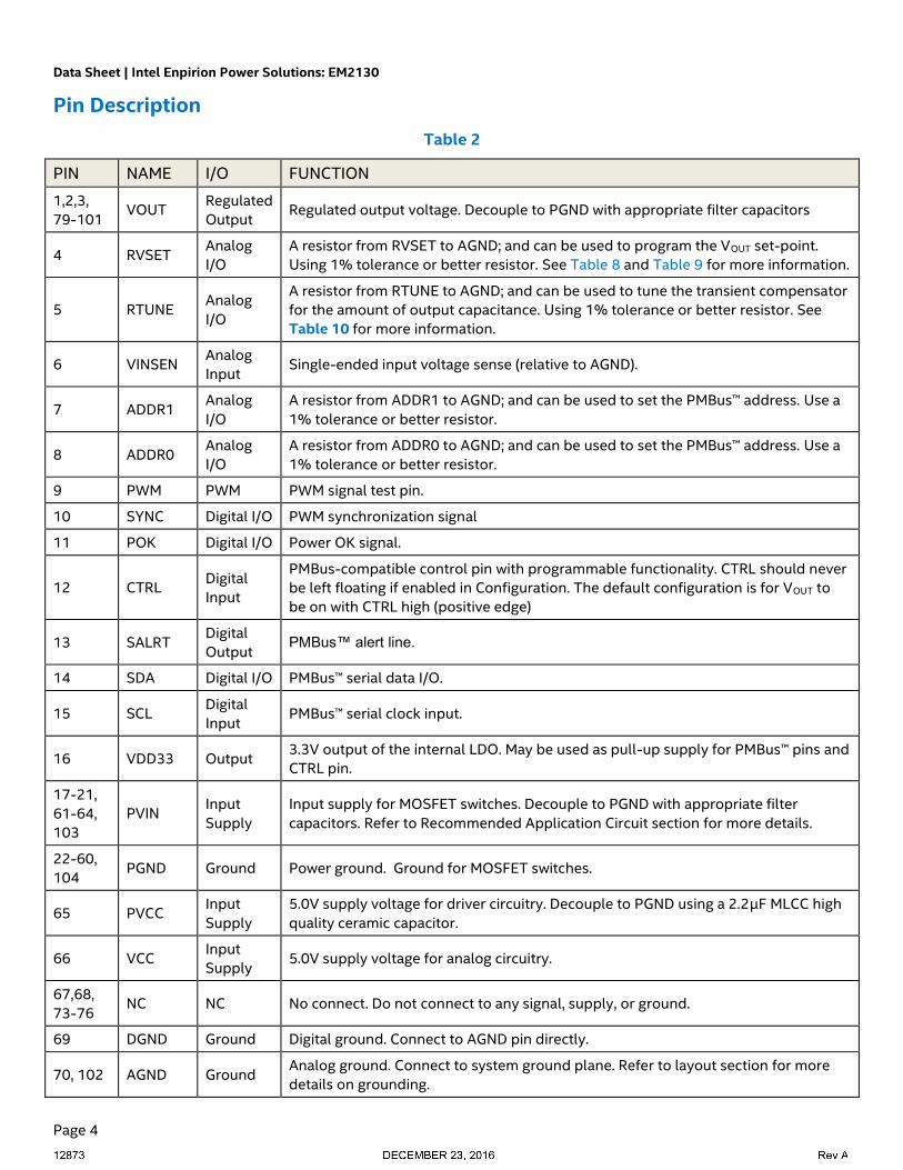
Pin Description
Table 2
PIN NAME I/O FUNCTION
1,2,3,
79-101 VOUT
Regulated
Output Regulated output voltage. Decouple to PGND with appropriate filter capacitors
4 RVSET Analog
I/O A resistor from RVSET to AGND; and can be used to program the VOUT set-point.
Using 1% tolerance or better resistor. See Table 8 and Table 9 for more information.
5 RTUNE Analog
I/O
A resistor from RTUNE to AGND; and can be used to tune the transient compensator
for the amount of output capacitance. Using 1% tolerance or better resistor. See
Table 10 for more information.
6 VINSEN Analog
Input Single-ended input voltage sense (relative to AGND).
7 ADDR1 Analog
I/O A resistor from ADDR1 to AGND; and can be used to set the PMBus™ address. Use a
1% tolerance or better resistor.
8 ADDR0 Analog
I/O A resistor from ADDR0 to AGND; and can be used to set the PMBus™ address. Use a
1% tolerance or better resistor.
9 PWM PWM PWM signal test pin.
10 SYNC Digital I/O PWM synchronization signal
11 POK Digital I/O Power OK signal.
12 CTRL Digital
Input
PMBus-compatible control pin with programmable functionality. CTRL should never
be left floating if enabled in Configuration. The default configuration is for VOUT to
be on with CTRL high (positive edge)
13 SALRT Digital
Output PMBus™ alert line.
14 SDA Digital I/O PMBus™ serial data I/O.
15 SCL Digital
Input PMBus™ serial clock input.
16 VDD33 Output 3.3V output of the internal LDO. May be used as pull-up supply for PMBus™ pins and
CTRL pin.
17-21,
61-64,
103 PVIN
Input
Supply Input supply for MOSFET switches. Decouple to PGND with appropriate filter
capacitors. Refer to Recommended Application Circuit section for more details.
22-60,
104 PGND Ground Power ground. Ground for MOSFET switches.
65 PVCC Input
Supply 5.0V supply voltage for driver circuitry. Decouple to PGND using a 2.2µF MLCC high
quality ceramic capacitor.
66 VCC Input
Supply 5.0V supply voltage for analog circuitry.
67,68,
73-76 NC NC No connect. Do not connect to any signal, supply, or ground.
69 DGND Ground Digital ground. Connect to AGND pin directly.
70, 102 AGND Ground Analog ground. Connect to system ground plane. Refer to layout section for more
details on grounding.
Data Sheet | Intel Enpirion Power Solutions: EM2130
Page 5
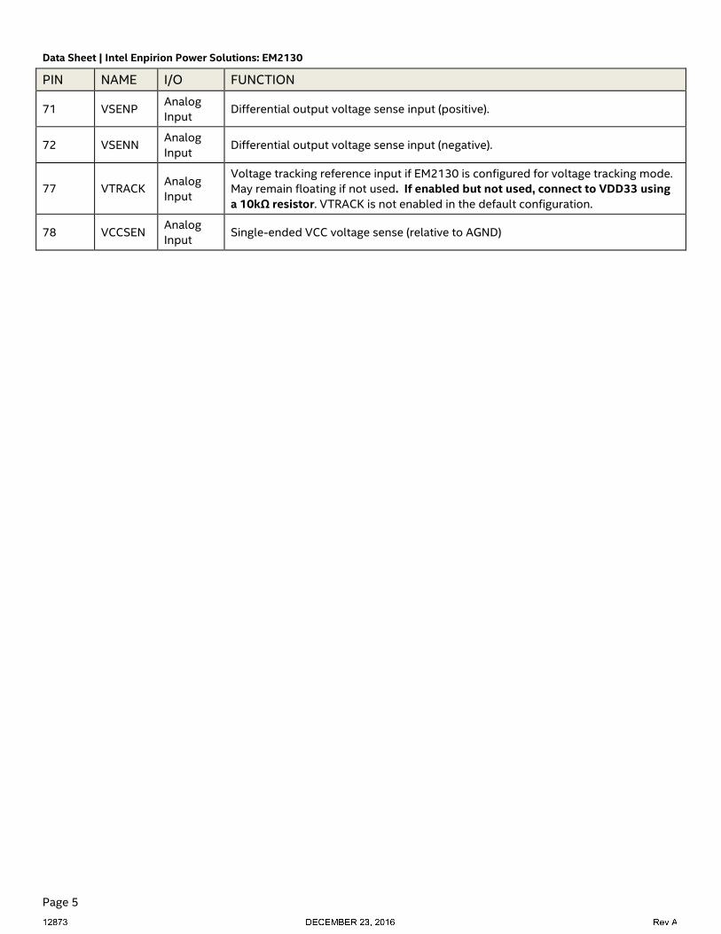
PIN NAME I/O FUNCTION
71 VSENP Analog
Input Differential output voltage sense input (positive).
72 VSENN Analog
Input Differential output voltage sense input (negative).
77 VTRACK Analog
Input
Voltage tracking reference input if EM2130 is configured for voltage tracking mode.
May remain floating if not used. If enabled but not used, connect to VDD33 using
a 10kΩ resistor. VTRACK is not enabled in the default configuration.
78 VCCSEN Analog
Input Single-ended VCC voltage sense (relative to AGND)
Data Sheet | Intel Enpirion Power Solutions: EM2130
Page 6
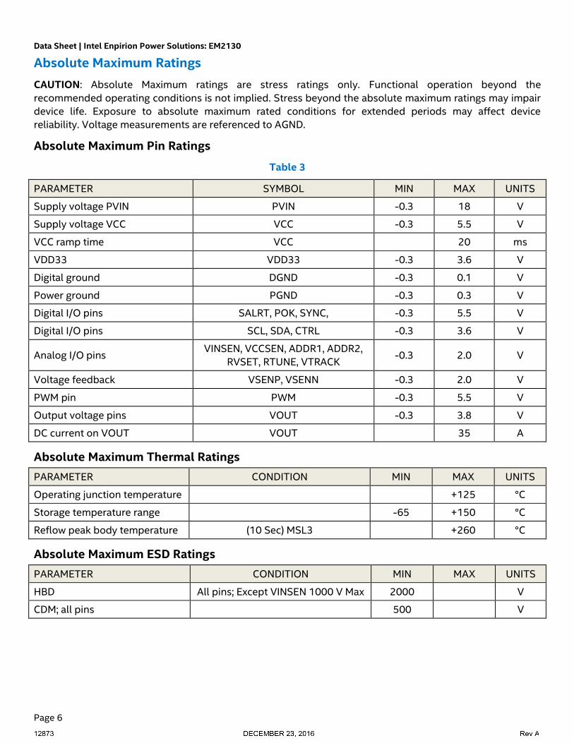
Absolute Maximum Ratings
CAUTION: Absolute Maximum ratings are stress ratings only. Functional operation beyond the
recommended operating conditions is not implied. Stress beyond the absolute maximum ratings may impair
device life. Exposure to absolute maximum rated conditions for extended periods may affect device
reliability. Voltage measurements are referenced to AGND.
Absolute Maximum Pin Ratings
Table 3
PARAMETER SYMBOL MIN MAX UNITS
Supply voltage PVIN PVIN -0.3 18 V
Supply voltage VCC VCC -0.3 5.5 V
VCC ramp time VCC 20 ms
VDD33 VDD33 -0.3 3.6 V
Digital ground DGND -0.3 0.1 V
Power ground PGND -0.3 0.3 V
Digital I/O pins SALRT, POK, SYNC, -0.3 5.5 V
Digital I/O pins SCL, SDA, CTRL -0.3 3.6 V
Analog I/O pins VINSEN, VCCSEN, ADDR1, ADDR2,
RVSET, RTUNE, VTRACK -0.3 2.0 V
Voltage feedback VSENP, VSENN -0.3 2.0 V
PWM pin PWM -0.3 5.5 V
Output voltage pins VOUT -0.3 3.8 V
DC current on VOUT VOUT 35 A
Absolute Maximum Thermal Ratings
PARAMETER CONDITION MIN MAX UNITS
Operating junction temperature +125 °C
Storage temperature range -65 +150 °C
Reflow peak body temperature (10 Sec) MSL3 +260 °C
Absolute Maximum ESD Ratings
PARAMETER CONDITION MIN MAX UNITS
HBD All pins; Except VINSEN 1000 V Max 2000 V
CDM; all pins 500 V
Data Sheet | Intel Enpirion Power Solutions: EM2130
Page 7
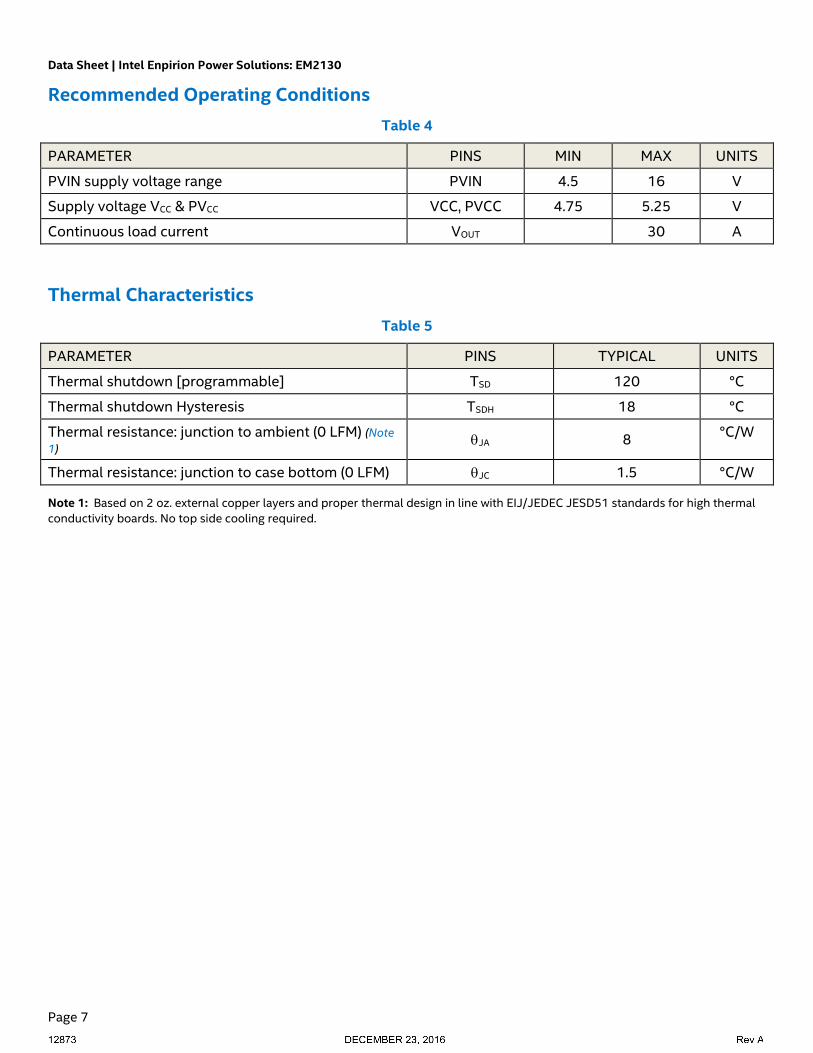
Recommended Operating Conditions
Table 4
PARAMETER PINS MIN MAX UNITS
PVIN supply voltage range PVIN 4.5 16 V
Supply voltage VCC & PVCC VCC, PVCC 4.75 5.25 V
Continuous load current VOUT 30 A
Thermal Characteristics
Table 5
PARAMETER PINS TYPICAL UNITS
Thermal shutdown [programmable] TSD 120 °C
Thermal shutdown Hysteresis TSDH 18 °C
Thermal resistance: junction to ambient (0 LFM) (Note
1) JA 8
°C/W
Thermal resistance: junction to case bottom (0 LFM) JC 1.5 °C/W
Note 1: Based on 2 oz. external copper layers and proper thermal design in line with EIJ/JEDEC JESD51 standards for high thermal
conductivity boards. No top side cooling required.

Data Sheet | Intel Enpirion Power Solutions: EM2130
Page 8
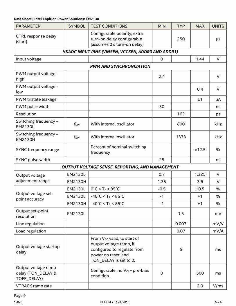
Electrical Characteristics
PVIN = 12V and VCC = 5.0V. The minimum and maximum values are over the operating ambient temperature
range (-40°C to 85°C) unless otherwise noted. Typical values are at TA = 25°C.
Table 6
PARAMETER SYMBOL TEST CONDITIONS MIN TYP MAX UNITS
SUPPLY CHARACTERISTICS
PVIN supply voltage
range PVIN 4.5
16 V
PVIN supply quiescent
current
Device switching; no load; fsw =
800 kHz; VOUT = 1.0V 40
mA
Device not switching 1
VCC supply voltage
range VCC 4.75 5.0 5.25 V
VCC UVLO rising 4.4 V
VCC UVLO falling 4.2 V
VCC supply current
Normal operation; no load;
fsw = 800 kHz 80 mA
Idle; communication and
telemetry only; no switching 30 mA
Disabled (VCC ≤ 2.8V) 900 µA
INTERNALLY GENERATED SUPPLY VOLTAGE
VDD33 voltage range VDD33 3.0 3.3 3.6
VDD33 output current 2 mA
DIGITAL I/O PINS (POK, SYNC)
Input high voltage 2.0 5.5 V
Input low voltage 0 0.8 V
Output high voltage 2.4 VDD33 V
Output low voltage 0.4 V
Input leakage current ±1 µA
Output current - source 2.0 mA
Output current - sink 2.0 mA
DIGITAL I/O PIN (CTRL)
Input high voltage 2.0 3.6 V
Input low voltage -0.3 0.8 V
CTRL response delay
(stop)
Configurable polarity; extra
turn-off delay configurable
(assumes 0 s turn-off delay)
150 µs
Data Sheet | Intel Enpirion Power Solutions: EM2130
Page 9
PARAMETER SYMBOL TEST CONDITIONS MIN TYP MAX UNITS
CTRL response delay
(start)
Configurable polarity; extra
turn-on delay configurable
(assumes 0 s turn-on delay)
250 µs
HKADC INPUT PINS (VINSEN, VCCSEN, ADDR0 AND ADDR1)
Input voltage 0 1.44 V
PWM AND SYNCHRONIZATION
PWM output voltage -
high 2.4 V
PWM output voltage -
low 0.4 V
PWM tristate leakage ±1 µA
PWM pulse width 30 ns
Resolution 163 ps
Switching frequency –
EM2130L fSW With internal oscillator 800 kHz
Switching frequency –
EM2130H fSW With internal oscillator 1333 kHz
SYNC frequency range Percent of nominal switching
frequency ±12.5 %
SYNC pulse width 25 ns
OUTPUT VOLTAGE SENSE, REPORTING, AND MANAGEMENT
Output voltage
adjustment range
EM2130L 0.7 1.325 V
EM2130H 1.35 3.6 V
Output voltage set-
point accuracy
EM2130L 0˚C < TA < 85˚C -0.5 +0.5 %
EM2130L -40˚C < TA < 85˚C -1 +1 %
EM2130H -40˚C < TA < 85˚C -1 +1 %
Output set-point
resolution EM2130L 1.5 mV
Line regulation 0.007 mV/V
Load regulation 0.07 mV/A
Output voltage startup
delay
From VCC valid, to start of
output voltage ramp, if
configured to regulate from
power on reset, and
TON_DELAY is set to 0.
5 ms
Output voltage ramp
delay (TON_DELAY &
TOFF_DELAY)
Configurable, no VOUT pre-bias
condition. 0 500 ms
VTRACK ramp rate 2.0 V/ms

Data Sheet | Intel Enpirion Power Solutions: EM2130
Page 10
PARAMETER SYMBOL TEST CONDITIONS MIN TYP MAX UNITS
VTRACK range Without resistor divider 0 1.4 V
VTRACK offset voltage ±100 mV
OUTPUT CURRENT SENSE, REPORTING, AND MANAGEMENT
Current sense reporting
accuracy
25°C < TA < 85°C ±1.5 A
IOUT > 5A, TA = 25°C ±1 A
TEMPERATURE SENSE, REPORTING, AND MANAGEMENT
Temperature reporting
accuracy ±5 °C
Resolution 0.22 °C
FAULT MANAGEMENT PROTECTION FEATURES
PVIN UV threshold 3.96 V
PVIN OV threshold 16.5 V
VOUT OV threshold Percentage of output voltage 115 %
VOUT UV threshold Percentage of output voltage 85 %
IOUT OCP With 45A OCP setting 40 50 A
OTP threshold 120 °C
OTP hysteresis Fixed. 85 %
POK threshold On level 95 %
POK threshold Off level 90 %
SERIAL COMMUNICATION PMBUS DC CHARACTERISTICS
Input voltage – high
(VIH) SCL and SDA 1.11 V
Input voltage – low (VIL) SCL and SDA 0.8 V
Input leakage current SCL, SDA, SALRT, and CTRL. -10 10 µA
Output voltage – low
(VOL)
SDA and SALRT at rated pull-
up current of 20mA. 0.4 V
Nominal bus voltage SCL, SDA, and SALRT
termination voltage. 3.6 V

Data Sheet | Intel Enpirion Power Solutions: EM2130
Page 11
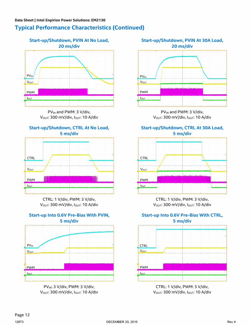
Typical Performance Characteristics
All the performance curves are measured with EM2130 evaluation board at 25°C ambient temperature
unless otherwise noted. The output capacitors configuration for the evaluation board is 2 x 470 µF (3 mΩ
ESR) + 4 x 100 µF (Ceramic) + 4 x 47 µF (Ceramic).
Efficiency, VIN = 12V Efficiency, VIN = 5V
EM2130L Thermal Derating, No Airflow EM2130H Thermal Derating, No Airflow
EM2130L Line Regulation, VOUT = 0.9V EM2130L Load Regulation, VOUT = 0.9V
Data Sheet | Intel Enpirion Power Solutions: EM2130
Page 12
Typical Performance Characteristics (Continued)
Start-up/Shutdown, PVIN At No Load,
20 ms/div
Start-up/Shutdown, PVIN At 30A Load,
20 ms/div
PVIN and PWM: 3 V/div, VOUT: 300 mV/div, IOUT: 10 A/div
PVIN and PWM: 3 V/div,
VOUT: 300 mV/div, IOUT: 10 A/div
Start-up/Shutdown, CTRL At No Load,
5 ms/div
Start-up/Shutdown, CTRL At 30A Load,
5 ms/div
CTRL: 1 V/div, PWM: 3 V/div,
VOUT: 300 mV/div, IOUT: 10 A/div
CTRL: 1 V/div, PWM: 3 V/div,
VOUT: 300 mV/div, IOUT: 10 A/div
Start-up Into 0.6V Pre-Bias With PVIN,
5 ms/div
Start-up Into 0.6V Pre-Bias With CTRL,
5 ms/div
PVIN: 3 V/div, PWM: 3 V/div,
VOUT: 300 mV/div, IOUT: 10 A/div
CTRL: 1 V/div, PWM: 3 V/div,
VOUT: 300 mV/div, IOUT: 10 A/div
PVIN
VOUT
PWM
IOUT
VOUT
IOUT
PVIN
PWM
CTRL
VOUT
PWM
IOUT
CTRL
VOUT
PWM
IOUT
PVIN
VOUT
PWM
IOUT
CTRL
VOUT
PWM
IOUT

Data Sheet | Intel Enpirion Power Solutions: EM2130
Page 13
Typical Performance Characteristics (Continued)
Output Voltage Ripple,
No Load
Output Voltage Ripple,
30A Load
VIN = 12V, VOUT = 0.9V
1 µs/div, VOUT: 10 mV/div, 20 MHz bandwidth
VIN = 12V, VOUT = 0.9V
1 µs/div, VOUT: 10 mV/div, 20 MHz bandwidth
Output Voltage Transient Response,
Load Step From 0A To 15A
Output Voltage Transient Response,
Load Step From 15A To 30A
VIN = 12V, VOUT = 0.9V, 100µs/div
VOUT: 30 mV/div, IOUT: 5 A/div, 15 A/µs
VIN = 12V, VOUT = 0.9V, 100µs/div
VOUT: 30 mV/div, IOUT: 5 A/div, 15 A/µs
Output Voltage Transient Response,
Load Step From 0A To 15A
Output Voltage Transient Response,
Load Step From 0A To 15A
VIN = 12V, VOUT = 0.9V, 2µs/div
VOUT: 10 mV/div, IOUT: 5 A/div, 100 A/µs
VIN = 12V, VOUT = 0.9V, 10µs/div
VOUT: 10 mV/div, IOUT: 5 A/div, 1 A/µs
VOUT
IOUT
VOUT
IOUT
VOUT
IOUT
VOUT
IOUT
VOUT
IOUT
VOUT
IOUT
Data Sheet | Intel Enpirion Power Solutions: EM2130
Page 14
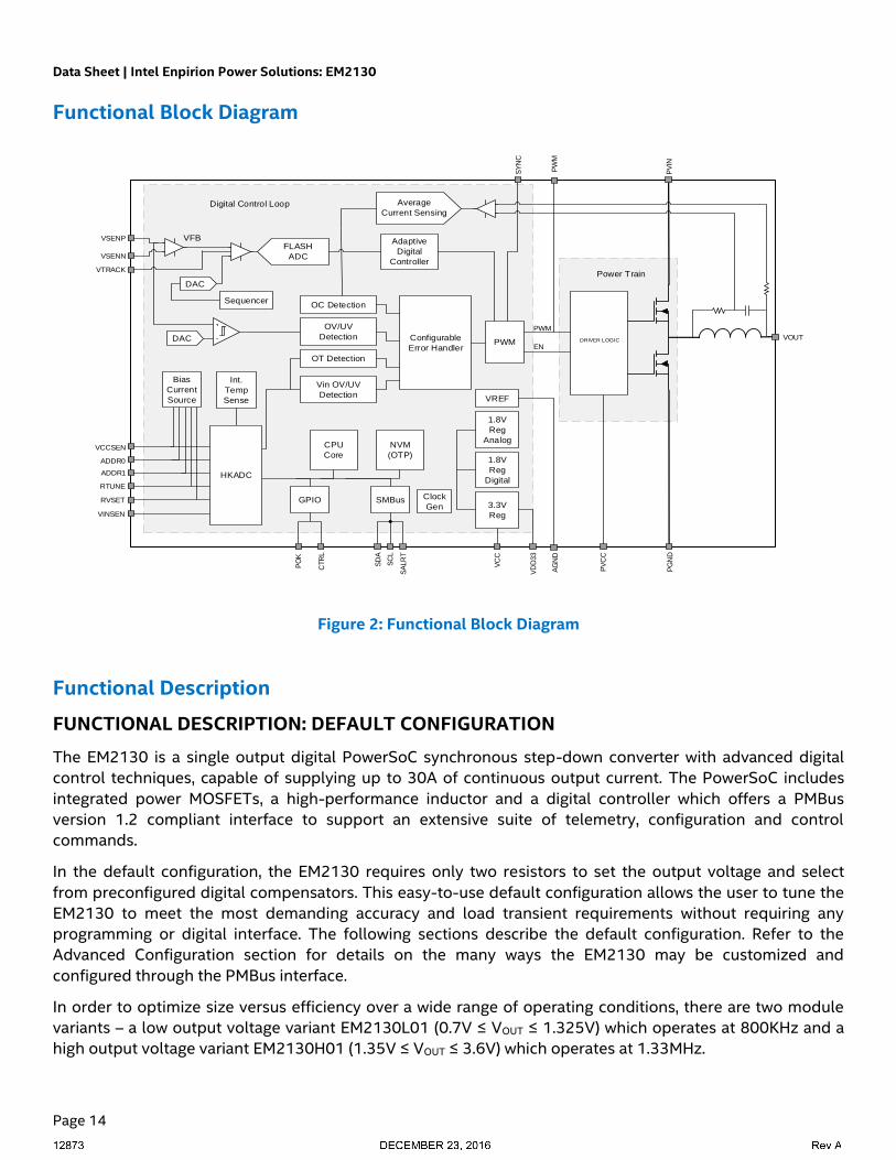
Functional Block Diagram
Sequencer
Configurable
Error Handler
Clock
Gen
OV/UV
Detection
OC Detection
FLASH
ADC
CPU
Core
NVM
(OTP)1.8V
Reg
Digital
1.8V
Reg
Analog
VREF
VSENP
VSENN
VC
C
Adaptive
Digital
Controller
PWM
VFB
Digital Control Loop
Int.
Temp
Sense
3.3V
Reg
SMBusGPIO
PO
K
CTR
L
SD
A
SC
L
SA
LR
T
DAC
DAC
Average
Current Sensing
OT Detection
Vin OV/UV
Detection
VCCSEN
ADDR0
RVSET
VD
D33
RTUNE
PWM
EN
VINSEN
VTRACK
HKADC
Bias
Current
Source
ADDR1
SY
NC
DRIVER LOGIC
Power Train
PV
CC
PV
INP
GN
D
VOUT
AG
ND
PW
M
Figure 2: Functional Block Diagram
Functional Description
FUNCTIONAL DESCRIPTION: DEFAULT CONFIGURATION
The EM2130 is a single output digital PowerSoC synchronous step-down converter with advanced digital
control techniques, capable of supplying up to 30A of continuous output current. The PowerSoC includes
integrated power MOSFETs, a high-performance inductor and a digital controller which offers a PMBus
version 1.2 compliant interface to support an extensive suite of telemetry, configuration and control
commands.
In the default configuration, the EM2130 requires only two resistors to set the output voltage and select
from preconfigured digital compensators. This easy-to-use default configuration allows the user to tune the
EM2130 to meet the most demanding accuracy and load transient requirements without requiring any
programming or digital interface. The following sections describe the default configuration. Refer to the
Advanced Configuration section for details on the many ways the EM2130 may be customized and
configured through the PMBus interface.
In order to optimize size versus efficiency over a wide range of operating conditions, there are two module
variants – a low output voltage variant EM2130L01 (0.7V ≤ VOUT ≤ 1.325V) which operates at 800KHz and a
high output voltage variant EM2130H01 (1.35V ≤ VOUT ≤ 3.6V) which operates at 1.33MHz.

Data Sheet | Intel Enpirion Power Solutions: EM2130
Page 15
The advanced digital control loop works as a voltage-mode controller using a PID-type compensation. The
basic structure of the controller is shown in Figure 3. The EM2130 controller features two PID compensators
for steady-state operation and fast transient operation. Fast, reliable switching between the different
compensation modes ensures good transient performance and quiet steady state performance. The EM2130
has been pre-programmed with a range of default compensation coefficients which lets the user select the
best compensation for the best transient response and stability for the output capacitance of the system.
The EM2130 uses two additional technologies to improve transient performance. First, the EM2130 uses
over-sampling techniques to acquire fast, accurate, and continuous information about the output voltage so
that the device can react quickly to any changes in output voltage. Second, a non-linear gain adjustment is
applied during large load transients to boost the loop gain and reduce the settling time.
Digital PID Compensator
Steady-State
Transient
Coefficients
Non-linearGain
Operation Mode
Detection
Digital Error Signal
Duty Cycle
Figure 3: Simplified Block Diagram Of The Digital Compensation
In the default configuration, the EM2130 offers a complete suite of fault warnings and protections. Input and
output Under Voltage Lock-Out (UVLO) and Over Voltage Lock-Out (OVLO) conditions are continuously
monitored. A dedicated ADC is used to provide fast and accurate current information over the switching
period allowing for fast Over-Current Protection (OCP) response. Over Temperature Protection (OTP) is
accomplished by direct monitoring of the device’s internal temperature.
POWER ON RESET
The EM2130 employs an internal power-on-reset (POR) circuit to ensure proper start-up and shut down with
a changing supply voltage. Once the VCC supply voltage increases above the POR threshold voltage, the
EM2130 begins the internal start-up process. Upon its completion, the device is ready for operation.
Two separate input voltage supplies are necessary to operate, PVIN (4.5V to 16V) and VCC (4.75V to 5.25V).
Both of these voltage rails must be monitored for proper power-up and to protect the power MOSFETs
under various input power fault conditions. A voltage divider on each input voltage supply connected to
VINSEN for the power rail (PVIN) and VCCSEN for the supply rail (VC) is used for digital monitoring of the
supplies.
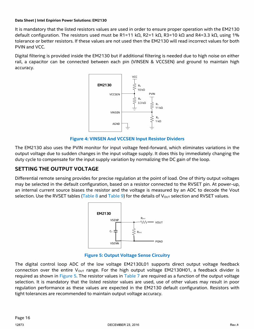
As illustrated in Figure 4, the values of resistors R1, R2, R3 and R4 are chosen so the internal monitor ADC
does not saturate within the appropriate ranges. This allows the EM2130 telemetry to report when the
recommended operation voltage has been exceeded.
Data Sheet | Intel Enpirion Power Solutions: EM2130
Page 16
It is mandatory that the listed resistors values are used in order to ensure proper operation with the EM2130
default configuration. The resistors used must be R1=11 kΩ, R2=1 kΩ, R3=10 kΩ and R4=3.3 kΩ, using 1%
tolerance or better resistors. If these values are not used then the EM2130 will read incorrect values for both
PVIN and VCC.
Digital filtering is provided inside the EM2130 but if additional filtering is needed due to high noise on either
rail, a capacitor can be connected between each pin (VINSEN & VCCSEN) and ground to maintain high
accuracy.
EM2130
PVIN
VINSEN
1 k
11 k
AGND
R1
R2
VCCSEN
VCC
10 k
3.3 k
R3
R4
Figure 4: VINSEN And VCCSEN Input Resistor Dividers
The EM2130 also uses the PVIN monitor for input voltage feed-forward, which eliminates variations in the
output voltage due to sudden changes in the input voltage supply. It does this by immediately changing the
duty cycle to compensate for the input supply variation by normalizing the DC gain of the loop.
SETTING THE OUTPUT VOLTAGE
Differential remote sensing provides for precise regulation at the point of load. One of thirty output voltages
may be selected in the default configuration, based on a resistor connected to the RVSET pin. At power-up,
an internal current source biases the resistor and the voltage is measured by an ADC to decode the Vout
selection. Use the RVSET tables (Table 8 and Table 9) for the details of VOUT selection and RVSET values.
EM2130
VOUT
PGND
VSENP
RDIV2
RDIV1
VSENN
CA
Figure 5: Output Voltage Sense Circuitry
The digital control loop ADC of the low voltage EM2130L01 supports direct output voltage feedback
connection over the entire VOUT range. For the high output voltage EM2130H01, a feedback divider is
required as shown in Figure 5. The resistor values in Table 7 are required as a function of the output voltage
selection. It is mandatory that the listed resistor values are used, use of other values may result in poor
regulation performance as these values are expected in the EM2130 default configuration. Resistors with
tight tolerances are recommended to maintain output voltage accuracy.

Data Sheet | Intel Enpirion Power Solutions: EM2130
Page 17
The resistors in the feedback path also form a low-pass filter with the internal capacitor, CA, for removing
high-frequency disturbances from the sense signals. Place these components as close as possible to the
EM2130 for best filtering performance.
Table 7: Output Voltage Feedback Component
Module VOUT RDIV1 RDIV2
EM2130L01 0.7V ≤ VOUT ≤ 1.325V 2 kΩ Open
EM2130H01 1.35V ≤ VOUT ≤ 2.6V 2 kΩ 2 kΩ
EM2130H01 2.6V < VOUT ≤ 3.6V 2 kΩ 1 kΩ
Table 8: Supported Configuation Voltage Values For EM2130L01 Output Voltage
RVSET Resistor VOUT External Resistor Divider
0kΩ Reserved R1DIV = 2kΩ, R2DIV = open
0.392kΩ Reserved R1DIV = 2kΩ, R2DIV = open
0.576kΩ Reserved R1DIV = 2kΩ, R2DIV = open
0.787kΩ Reserved R1DIV = 2kΩ, R2DIV = open
1.000kΩ 1.325V R1DIV = 2kΩ, R2DIV = open
1.240kΩ 1.3V R1DIV = 2kΩ, R2DIV = open
1.500kΩ 1.275V R1DIV = 2kΩ, R2DIV = open
1.780kΩ 1.25V R1DIV = 2kΩ, R2DIV = open
2.100kΩ 1.225V R1DIV = 2kΩ, R2DIV = open
2.430kΩ 1.2V R1DIV = 2kΩ, R2DIV = open
2.800kΩ 1.175V R1DIV = 2kΩ, R2DIV = open
3.240kΩ 1.15V R1DIV = 2kΩ, R2DIV = open
3.740kΩ 1.12V R1DIV = 2kΩ, R2DIV = open
4.220kΩ 1.1V R1DIV = 2kΩ, R2DIV = open
4.750kΩ 1.075V R1DIV = 2kΩ, R2DIV = open
5.360kΩ 1.05V R1DIV = 2kΩ, R2DIV = open
6.040kΩ 1.03V R1DIV = 2kΩ, R2DIV = open
6.810kΩ 1.0V R1DIV = 2kΩ, R2DIV = open
7.680kΩ 0.975V R1DIV = 2kΩ, R2DIV = open
8.660kΩ 0.95V R1DIV = 2kΩ, R2DIV = open
9.530kΩ 0.925V R1DIV = 2kΩ, R2DIV = open
10.500kΩ 0.9V R1DIV = 2kΩ, R2DIV = open
11.800kΩ 0.875V R1DIV = 2kΩ, R2DIV = open
13.000kΩ 0.85V R1DIV = 2kΩ, R2DIV = open

Data Sheet | Intel Enpirion Power Solutions: EM2130
Page 18
RVSET Resistor VOUT External Resistor Divider
14.300kΩ 0.825V R1DIV = 2kΩ, R2DIV = open
15.800kΩ 0.8V R1DIV = 2kΩ, R2DIV = open
17.400kΩ 0.775V R1DIV = 2kΩ, R2DIV = open
19.100kΩ 0.75V R1DIV = 2kΩ, R2DIV = open
21.000kΩ 0.725V R1DIV = 2kΩ, R2DIV = open
23.200kΩ 0.7V R1DIV = 2kΩ, R2DIV = open
Table 9: Supported Configuration Voltage Values For EM2130H01 Output Voltage
RVSET Resistor VOUT External Resistor Divider
0kΩ Reserved R1DIV = 2kΩ, R2DIV = 1kΩ
0.392kΩ Reserved R1DIV = 2kΩ, R2DIV = 1kΩ
0.576kΩ 3.3V R1DIV = 2kΩ, R2DIV = 1kΩ
0.787kΩ 3.2V R1DIV = 2kΩ, R2DIV = 1kΩ
1.000kΩ 3.1V R1DIV = 2kΩ, R2DIV = 1kΩ
1.240kΩ 3.0V R1DIV = 2kΩ, R2DIV =1kΩ
1.500kΩ 2.9V R1DIV = 2kΩ, R2DIV = 1kΩ
1.780kΩ 2.8V R1DIV = 2kΩ, R2DIV = 1kΩ
2.100kΩ 2.7V R1DIV = 2kΩ, R2DIV = 1kΩ
2.430kΩ 2.6V R1DIV = 2kΩ, R2DIV = 2kΩ
2.800kΩ 2.5V R1DIV = 2kΩ, R2DIV = 2kΩ
3.240kΩ 2.4V R1DIV = 2kΩ, R2DIV = 2kΩ
3.740kΩ 2.3V R1DIV = 2kΩ, R2DIV = 2kΩ
4.220kΩ 2.2V R1DIV = 2kΩ, R2DIV = 2kΩ
4.750kΩ 2.1V R1DIV = 2kΩ, R2DIV = 2kΩ
5.360kΩ 2.0V R1DIV = 2kΩ, R2DIV = 2kΩ
6.040kΩ 1.9V R1DIV = 2kΩ, R2DIV = 2kΩ
6.810kΩ 1.8V R1DIV = 2kΩ, R2DIV = 2kΩ
7.680kΩ 1.75V R1DIV = 2kΩ, R2DIV = 2kΩ
8.660kΩ 1.7V R1DIV = 2kΩ, R2DIV = 2kΩ
9.530kΩ 1.65V R1DIV = 2kΩ, R2DIV = 2kΩ
10.500kΩ 1.6V R1DIV = 2kΩ, R2DIV = 2kΩ
11.800kΩ 1.55V R1DIV = 2kΩ, R2DIV = 2kΩ
13.000kΩ 1.5V R1DIV = 2kΩ, R2DIV = 2kΩ
Data Sheet | Intel Enpirion Power Solutions: EM2130
Page 19
RVSET Resistor VOUT External Resistor Divider
14.300kΩ 1.475V R1DIV = 2kΩ, R2DIV = 2kΩ
15.800kΩ 1.45V R1DIV = 2kΩ, R2DIV = 2kΩ
17.400kΩ 1.425V R1DIV = 2kΩ, R2DIV = 2kΩ
19.100kΩ 1.4V R1DIV = 2kΩ, R2DIV = 2kΩ
21.000kΩ 1.375V R1DIV = 2kΩ, R2DIV = 2kΩ
23.200kΩ 1.35V R1DIV = 2kΩ, R2DIV = 2kΩ
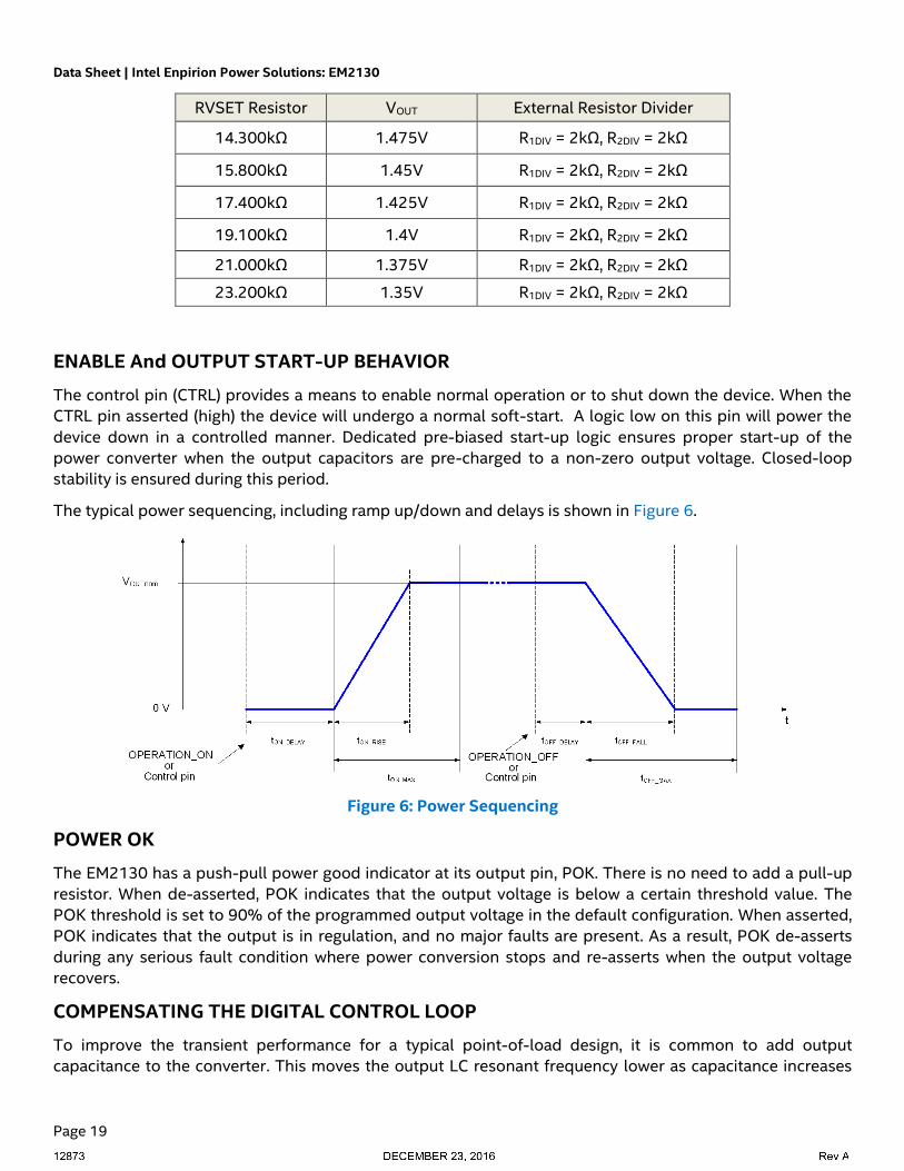
ENABLE And OUTPUT START-UP BEHAVIOR
The control pin (CTRL) provides a means to enable normal operation or to shut down the device. When the
CTRL pin asserted (high) the device will undergo a normal soft-start. A logic low on this pin will power the
device down in a controlled manner. Dedicated pre-biased start-up logic ensures proper start-up of the
power converter when the output capacitors are pre-charged to a non-zero output voltage. Closed-loop
stability is ensured during this period.
The typical power sequencing, including ramp up/down and delays is shown in Figure 6.
Figure 6: Power Sequencing
POWER OK
The EM2130 has a push-pull power good indicator at its output pin, POK. There is no need to add a pull-up
resistor. When de-asserted, POK indicates that the output voltage is below a certain threshold value. The
POK threshold is set to 90% of the programmed output voltage in the default configuration. When asserted,
POK indicates that the output is in regulation, and no major faults are present. As a result, POK de-asserts
during any serious fault condition where power conversion stops and re-asserts when the output voltage
recovers.
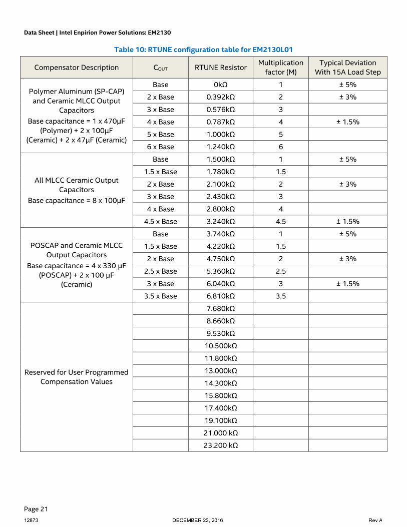
COMPENSATING THE DIGITAL CONTROL LOOP
To improve the transient performance for a typical point-of-load design, it is common to add output
capacitance to the converter. This moves the output LC resonant frequency lower as capacitance increases

Data Sheet | Intel Enpirion Power Solutions: EM2130
Page 20
which results in lower bandwidth, lower phase margin, and longer settling times unless the control loop is
compensated for added capacitance.
However, with EM2130 the user does not need to be concerned with, or even understand, the details of
control loop compensation techniques. The default configuration allows users to select from preconfigured
PID control loop settings (known as compensators) through the use of pin-strapping. A single resistor from
the RTUNE pin to AGND informs the EM2130 of the compensator selection.
The selection of the compensator is driven first by the type of output capacitors used, as the ESL and ESR of
different capacitor types demands different PID coefficients to optimize transient deviation and recovery
characteristics. An all ceramic output capacitor design requires a different compensator than a design with a
combination of ceramic and polymer capacitors, i.e. POSCAP. Table 11 shows several output capacitor part
number recommendations.
The five different compensators can then be subdivided into groups of six each whereby the initial
capacitance value in the appropriate compensator can be scaled upwards by multiplication factor M to
match the additional capacitance.
Data Sheet | Intel Enpirion Power Solutions: EM2130
Page 21
Table 10: RTUNE configuration table for EM2130L01
Compensator Description COUT RTUNE Resistor Multiplication
factor (M)
Typical Deviation
With 15A Load Step
Polymer Aluminum (SP-CAP)
and Ceramic MLCC Output
Capacitors
Base capacitance = 1 x 470µF
(Polymer) + 2 x 100µF
(Ceramic) + 2 x 47µF (Ceramic)
Base 0kΩ 1 ± 5%
2 x Base 0.392kΩ 2 ± 3%
3 x Base 0.576kΩ 3
4 x Base 0.787kΩ 4 ± 1.5%
5 x Base 1.000kΩ 5
6 x Base 1.240kΩ 6
All MLCC Ceramic Output
Capacitors
Base capacitance = 8 x 100µF
Base 1.500kΩ 1 ± 5%
1.5 x Base 1.780kΩ 1.5
2 x Base 2.100kΩ 2 ± 3%
3 x Base 2.430kΩ 3
4 x Base 2.800kΩ 4
4.5 x Base 3.240kΩ 4.5 ± 1.5%
POSCAP and Ceramic MLCC
Output Capacitors
Base capacitance = 4 x 330 µF
(POSCAP) + 2 x 100 µF
(Ceramic)
Base 3.740kΩ 1 ± 5%
1.5 x Base 4.220kΩ 1.5
2 x Base 4.750kΩ 2 ± 3%
2.5 x Base 5.360kΩ 2.5
3 x Base 6.040kΩ 3 ± 1.5%
3.5 x Base 6.810kΩ 3.5
Reserved for User Programmed
Compensation Values
7.680kΩ
8.660kΩ
9.530kΩ
10.500kΩ
11.800kΩ
13.000kΩ
14.300kΩ
15.800kΩ
17.400kΩ
19.100kΩ
21.000 kΩ
23.200 kΩ
Data Sheet | Intel Enpirion Power Solutions: EM2130
Page 22
Table 11: Recommended Output Capacitors
Description Manufacturer P/N
470µF, 2.5V, ESR 3mΩ SP-CAP Panasonic EEFGX0E471R
330µF, 6.3V, ESR 9 mΩ POSCAP Panasonic 6TPF330M9L
330µF, 2.5V, ESR 9 mΩ POSCAP Kemet T520B337M2R5ATE009
100µF, 6.3V, X5R, 1206 Ceramic Kemet C1206C107M9PACTU
47µF, 6.3V, X5R 1206 Ceramic Murata GRM31CR60J476ME19L
OUTPUT CAPACITOR RECOMMENDATION
The output filter capacitors can be configured as a combination of local output filter capacitors that absorb
the AC switching currents generated by the converter and bulk decoupling capacitors close to the device
supply pins; this recommendation refers only to the local filter capacitor requirements. Please consult the
documentation for your particular FPGA, ASIC, processor, or memory block for the bulk decoupling capacitor
requirements.
Table 12 shows the minimum local decoupling capacitors requirements. Two of the local output filter
capacitors can be mounted on the PCB back-side to reduce the solution size. An example of the minimum
footprint layout is shown in Figure 7. The output filter capacitors should use X5R, X7R, or equivalent
dielectric with an appropriate voltage rating.
Table 12: Local Decoupling Requirements
Symbol Capacitor Recommendations
CIN 3 x 22µF (1206) + 1 x 10µF (0805) or 4 x 22µF (1206)
COUT 4 x 100µF (1206)
INPUT CAPACITOR RECOMMENDATION
The EM2130 input should be decoupled with at least three 22µF 1206 case size and one 10µF 0805 case
size MLCC ceramic capacitors or four 22µF MLCC 1206 case size ceramic capacitors. More bulk capacitor
may be needed only if there are long inductive traces at the input source or there is not enough source
capacitance.
These input decoupling ceramic capacitors can be mounted on the PCB back-side to reduce the solution
size. These input filter capacitors should have the appropriate voltage rating for the input voltage on PVIN,
and use a X5R, X7R, or equivalent dielectric rating. Y5V or equivalent dielectric formulations must not be
used as these lose too much capacitance with frequency, temperature and bias voltage.
The PVCC pin provides power to the gate drive of the internal high/low side power MOSFETs. The VCC pin
provides power to the internal digital controller. These two power inputs share the same supply voltage (5V
nominal), and should be bypassed with a single 2.2µF MLCC capacitor. To avoid switching noise injection
from PVCC to VCC, it is recommended a ferrite bead is inserted between PVCC and VCC pins as shown Figure
16.

Data Sheet | Intel Enpirion Power Solutions: EM2130
Page 23
Figure 7: Top And Bottom Layer Of The Minimum Footprint Layout Example
PROTECTION FEATURES
The EM2130 offers a complete suite of programmable fault warnings and protections. Input and output
Under Voltage Lock-Out (UVLO) and Over Voltage Lock-Out (OVLO) conditions are continuously monitored.
A dedicated ADC is used to provide fast and accurate current information during the entire switching period
to provide fast Over-Current Protection (OCP) response.
To prevent damage to the load, the EM2130 utilizes an output over-voltage protection circuit. The voltage at
VSENP is continuously compared with a configurable threshold using a high-speed analog comparator. If the
voltage exceeds the configured threshold, a fault response is generated and the PWM output is turned off.
The output voltage is also sampled, filtered, and compared with an output over-voltage warning threshold. If
the output voltage exceeds this threshold, a warning is generated and the preconfigured actions are
triggered. The EM2130 also monitors the output voltage with two lower thresholds. If the output voltage is
below the under-voltage warning level and above the under-voltage fault level, an output voltage under-
voltage warning is triggered. If the output voltage falls below the fault level, a fault event is generated.
Similar to output over and under voltage protection, the EM2130 monitors the input voltage at VINSEN
continuously with a configurable threshold. If the input voltage exceeds the over voltage threshold or is
below the under voltage threshold, the default response is generated.
Over Temperature Protection (OTP) is based on direct monitoring of the device’s internal temperature. If the
temperature exceeds the OTP threshold, the device will enter a soft-stop mode slowly ramping the output
voltage down until the temperature falls below the default recovery temperature.
The default fault response is zero delay and latch off for most fault conditions. The CTRL pin may be cycled
to clear the latch. Table 13 summarizes the default configurations that have been pre-programmed to the
device.
Data Sheet | Intel Enpirion Power Solutions: EM2130
Page 24
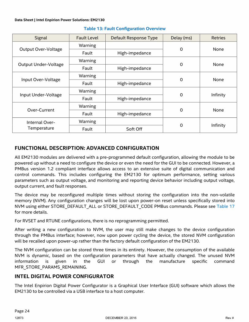
Table 13: Fault Configuration Overview
Signal Fault Level Default Response Type Delay (ms) Retries
Output Over-Voltage Warning
0 None Fault High-impedance
Output Under-Voltage Warning
0 None Fault High-impedance
Input Over-Voltage Warning
0 None Fault High-impedance
Input Under-Voltage Warning
0 Infinity Fault High-impedance
Over-Current Warning
0 None Fault High-impedance
Internal Over-
Temperature
Warning 0 Infinity
Fault Soft Off
FUNCTIONAL DESCRIPTION: ADVANCED CONFIGURATION
All EM2130 modules are delivered with a pre-programmed default configuration, allowing the module to be
powered up without a need to configure the device or even the need for the GUI to be connected. However, a
PMBus version 1.2 compliant interface allows access to an extensive suite of digital communication and
control commands. This includes configuring the EM2130 for optimum performance, setting various
parameters such as output voltage, and monitoring and reporting device behavior including output voltage,
output current, and fault responses.
The device may be reconfigured multiple times without storing the configuration into the non-volatile
memory (NVM). Any configuration changes will be lost upon power-on reset unless specifically stored into
NVM using either STORE_DEFAULT_ALL or STORE_DEFAULT_CODE PMBus commands. Please see Table 17
for more details.
For RVSET and RTUNE configurations, there is no reprogramming permitted.
After writing a new configuration to NVM, the user may still make changes to the device configuration
through the PMBus interface; however, now upon power cycling the device, the stored NVM configuration
will be recalled upon power-up rather than the factory default configuration of the EM2130.
The NVM configuration can be stored three times in its entirety. However, the consumption of the available
NVM is dynamic, based on the configuration parameters that have actually changed. The unused NVM
information is given in the GUI or through the manufacture specific command
MFR_STORE_PARAMS_REMAINING.
INTEL DIGITAL POWER CONFIGURATOR
The Intel Enpirion Digital Power Configurator is a Graphical User Interface (GUI) software which allows the
EM2130 to be controlled via a USB interface to a host computer.
Data Sheet | Intel Enpirion Power Solutions: EM2130
Page 25
The user can view the power supply’s status, I/O voltages, output current and fault conditions detected by
the device, program settings to the converter, and issue PMBus commands using the GUI. Most of the
parameters (for example, VOUT turn on/off time, protection and fault limits) can be configured and adjusted
within the GUI environment. These parameters can also be configured outside of the GUI environment using
the relevant PMBus™ commands.
The GUI also allows the user to easily create, modify, test and save a configuration file which may then be
used to permanently burn the configuration into NVM within a production test environment.
ALTERNATIVE OUTPUT VOLTAGE CONTROL METHODS
In the default configuration, output voltage selection is determined at power-up by the pin-strapped resistor
RVSET. This functionality can be disabled using the PMBus command MFR_PIN_CONFIG. When RVSET is
disabled, the output voltage will be determined by the nominal output voltage setting in the user
configuration. The EM2130 supports a subset of the output voltage commands outlined in the PMBus
specification. For example, the output voltage can be dynamically changed using the PMBus command
VOUT_COMMAND. When the output is being changed by the PMBus command, power good (POK) remains
at a logic high.
POWER SEQUENCING AND THE CONTROL (CTRL) PIN
Three different configuration options are supported to enable the output voltage. The device can be
configured to turn on after an OPERATION_ON command, via the assertion of the CTRL pin or a combination
of both per the PMBus convention. The EM2130 supports power sequencing features including
programmable ramp up/down and delays. The typical sequence of events is shown in Figure 6 and follows
the PMBus standard. The individual timing values shown in Figure 6 and Figure 8 can be configured using the
appropriate configuration setting in Intel Digital Power Configurator GUI.
PRE-BIASED START-UP AND SOFT-STOP
In systems with complex power architectures, there may be leakage paths from one supply domain which
charge capacitors in another supply domain leading to a pre-biased condition on one or more power
supplies. This condition is not idea and can be avoided through careful design, but is generally not harmful.
Attempting to discharge the pre-bias is not advised as it may force high current though the leakage path. The
EM2130 includes features to enable and disable into pre-biased output capacitors.
If the output capacitors are pre-biased when the EM2130 is enabled, start-up logic in the EM2130 ensures
that the output does not pull down the pre-biased voltage and the tON_RISE timing is preserved. Closed-loop
stability is ensured during the entire start-up sequence under all pre-bias conditions.
The EM2130 also supports pre-biased off, in which the output voltage ramp down to a user-defined level
(VOFF_nom) rather than to zero. After receiving the disable command, via PMBus command or the CTRL pin, the
EM2130 ramps down the output voltage to the predefined value. Once the value is reached, the output
driver into a tristate mode to avoid excessive currents through the leakage path.

Data Sheet | Intel Enpirion Power Solutions: EM2130
Page 26
Figure 8: Power Sequencing With Non-Zero Off Voltage
VOLTAGE TRACKING
The EM2130 can control the output voltage based on the external voltage applied to the VTRACK pin, thus
allowing sequencing of the output voltage from an external source. Pre-bias situations are also supported.
The VTRACK pin voltage is a single-ended input referenced to analog ground. Tracking mode is disabled by
default, but it can be enabled using the GUI software or via the manufacturer-specific PMBus command,
MFR_FEATURES_CTRL (see Table 17).
If VTRACK is not intended to be used, tie the VTRACK pin low or leaving it floating.
Figure 9: Power Sequencing Using VTRACK With Bias Voltage On VOUT
The set point voltage for the EM2130 is defined by the lower value of the VOUT setting or an external voltage
applied to the VTRACK pin. If the VTRACK voltage rises above the VOUT set point voltage, then the final
output voltage will be limited by the VOUT setting. If the tracking feature is enabled, but the VTRACK pin is
tied low or floating, then the output will never start as the VTRACK pin input is always the lower value and
will always be in control. Conversely, if tracking is enabled, but VTRACK is tied high, the output will start but
will follow the VOUT set point, not the VTRACK pin.
If tracking is used for sequencing, it is recommended that the VTRACK signal is kept greater than the VOUT
voltage. This ensures that the internal VOUT set point is used as the final steady-state output voltage and
accuracy is not a function of the externally applied VTARCK voltage. The tracking function will override a
programmed pre-bias off level (VOFF_nom).
VTRACK
t
VOUT
VTRACK
Pre-bias

Data Sheet | Intel Enpirion Power Solutions: EM2130
Page 27
DAC
VFB
VTRACK+
-
Set-Point(Defined by lower input value)
Figure 10: VTRACK Circuitry
The following figures demonstrate ratio-metric and simultaneous sequencing of the output voltage, which
can be accomplished by applying an appropriate external voltage on the VTRACK pin. When using the
VTRACK feature, the sequencing will be ratio-metric as shown in Figure 13 if an external resistor network is
used at the VTRACK pin as shown Figure 11. If no external resistors are used, the output sequence is
simultaneous as shown in Figure 14.
In the event that a feedback divider is not required, (such as when VOUT 1.4V) but the tracking voltage
applied to VTRACK is greater than 1.4V, then a 2kΩ resistor is required in series with the VTRACK pin to
minimize leakage current as shown in Figure 12.
In applications where a voltage divider is required on the output voltage, a voltage divider consisting of the
same values is also required for the VTRACK pin.
Figure 11: VTRACK Sense Circuitry with Resistor Divider
Figure 12: VTRACK Sense Circuitry (Input > 1.4V)

Data Sheet | Intel Enpirion Power Solutions: EM2130
Page 28
Figure 13: Ratiometric Sequencing Using VTRACK
Figure 14: Simultaneous Sequencing Using VTRACK
CLOCK SYNCHRONIZATION
The EM2130’s PWM synchronization feature allows the user to synchronize the switching frequency of
multiple devices. The SYNC pin can be configured as an input or an output.
When the SYNC pin is configured as input clock, the external clock need to be available before the EM2130
is enabled. The EM2130 will only lock to the external clock within 1ms after the device is enabled. After 1 ms
the device can be re-synchronized to the external clock signal by toggling VOUT or via PMBus MFR_RESYNC
command.
When the SYNC pin is configured as an output clock (sync out), there is no requirement to provide an
external clock to allow synchronization.
The EM2130 SYNC functionality maybe configured as an input or an output using Intel’s GUI software or via
the manufacturer-specific PMBus command, MFR_PIN_CONFIG. The default configuration for
synchronization control is OFF.
TEMPERATURE AND OUTPUT CURRENT MEASUREMENT
The EM2130 temperature sense block provides the device and the system with precision temperature
information over a wide range of temperatures (-40°C to +150°C). The temperature sense block measures
the digital controller temperature, which will be slightly lower than the powertrain junction temperature.
The EM2130 monitors output current by real-time, temperature compensated DCR current sensing across
the inductor. This real-time current waveform is then digitally filtered and averaged for accurate telemetry,
fault warning, and management.
Factory calibration has been performed for every EM2130 device to improve measurement accuracy over the
full output current range. This allows the EM2130 to correct for DCR manufacturing variations.
t
VTRACK
VOUT
V
t
VTRACK
VOUT
V

Data Sheet | Intel Enpirion Power Solutions: EM2130
Page 29
For over-current protection, an unfiltered ADC is used in order to minimize delays in protecting the device.
Because this measurement is unfiltered, the accuracy of the protection threshold is less than that of the
average current reading.
PROTECTION AND FAULT RESPONSE
The EM2130 monitors various signals during operation in order to detect fault conditions. Measured and
filtered signals are compared to a configurable set of warnings and fault thresholds. In typical usage, a
warning sets a status flag, but does not trigger a response; whereas a fault sets a status flag and generates a
response. The assertion of the SMBALERT signal can be configured to individual application requirements.
The EM2130 supports a number of different response types depending on the fault detected.
In the default configuration, the EM2130 responds to an over temperature event by ramping down VOUT in a
controlled manner at a slew rate defined by the TOFF_FALL value. This response type is termed “Soft-Off”. The
final state of the output signals depends on the value selected for VOFFnom.
For all other faults the EM2130 will respond by immediately turning off both the top-side MOSFET and low-
side MOSFET. This response type is termed “High-Impedance”.
For each fault response, a delay and a retry setting can be configured. If the delay-to-fault value is set to
non-zero, the EM2130 will not respond to a fault immediately. Instead it will delay the response by the
configured value and then reassesses the signal. If the fault remains present during the delay time, the
appropriate response will be triggered. If the fault is no longer present, the previous detection will be
disregarded.
If the delay-to-retry value is set to non-zero, the EM2130 will not attempt to restart immediately after fault
detection. Instead it will delay the restart by the configured value. If the fault is still present when attempting
to restart, the appropriate response will be triggered. If the fault is no longer present, the previous detection
will be disregarded. If the delay-to-fault is a non-zero value, then the delay-to-retry value will be a factor of
100 times greater than the delay-to-fault value.
The retry setting, i.e. the number of EM2130 restarts after a fault event, can be configured. This number can
be between zero and six. A setting of seven represents infinite retry operation. This setting is commonly
known as “Hiccup Mode.”
Data Sheet | Intel Enpirion Power Solutions: EM2130
Page 30
PMBus Functionality
INTRODUCTION
The EM2130 supports the PMBus protocol (version 1.2) to enable the use of configuration, monitoring, and
fault management features during run-time.
The PMBus host controller is connected to the EM2130 via the PMBus pins (SDA, SCL). A dedicated
SMBALERT pin is provided to notify the host that new status information is present.
The EM2130 supports packet correction (PEC) according to the PMBus™ specification.
The EM2130 supports more than 60 PMBus commands in addition to several manufacturer specific
commands related to output voltage, faults, telemetry, and more.
The EM2130 provides a PMBus set of synchronous communication lines, with serial clock input (SCL), serial
data I/O (SDA), and serial alarm output (SALRT) pins.
The communication lines provide 3.6V-tolerance, 1.8V I/O compatibility and open-drain outputs (SDA, SCL
and SALRT). The communication lines require external pull-up resistors; typical applications require pull-up
resistors on each end of the communication lines (typically values of 10 kΩ each), connected to VDD33 or an
alternative termination voltage. Please refer to the PMBus specification (www.pmbus.org) for full details.
The EM2130 provides configurable behavior for the SALRT pin to allow users to determine which fault or
warning conditions to communicate over the SALRT line. The default behavior of the controller ensures that
any fault or warning results in the EM2130 SALRT pin going low; the alert behavior is enabled for all faults
and warnings. You can deselect any of the faults or warnings so when one of these conditions occur, the
SALRT pin is not pulled low.
The EM2130 provides a PMBus compliant power conversion control signal through input CTRL. You can
configure input CTRL through the standard PMBus command ON_OFF_CONFIG.
By default configuration, the CTRL pin must be pulled high to enable operation and the PMBus command
OPERATION is ignored. You can override this function with the ON_OFF_CONFIG PMBus command.
Remote measurement and reporting of telemetry information at the power supply level provides feedback
on key parameters such as voltages, current levels, temperature, and energy, and allows reporting of
information such as faults and warning flags. With this information, data is collected and analyzed while the
power supply is in development, such as in the qualification or verification phases, or in the field, and system
level interaction such as power capping is implemented. Several telemetry parameters are supported by
standard PMBus commands.
The EM2130P supports PMBus output current telemetry through the READ_IOUT command and reports the
low-pass filtered, or DC, output current.
The standard PMBus command READ_VOUT supports output voltage telemetry.
The standard PMBus command READ_VIN supports input voltage telemetry.
The EM2130 supports temperature telemetry and reporting through standardized PMBus commands.
READ_TEMPERATURE_2 is mapped to the controller die temperature.
The standard PMBus command READ_FREQUENCY supports switching frequency monitoring. This
command returns the scaled frequency of the PWM output in kHz.
Data Sheet | Intel Enpirion Power Solutions: EM2130
Page 31
The EM2130 supports the LINEAR data format according to the PMBus specification. Note that in accordance
with the PMBus specification, all commands related to the output voltage are subject to the VOUT_MODE
settings.
A detailed description of the supported PMBus commands supported by the EM2130 can be found in
EM2130 Application Note – PMBus Commands Guide.
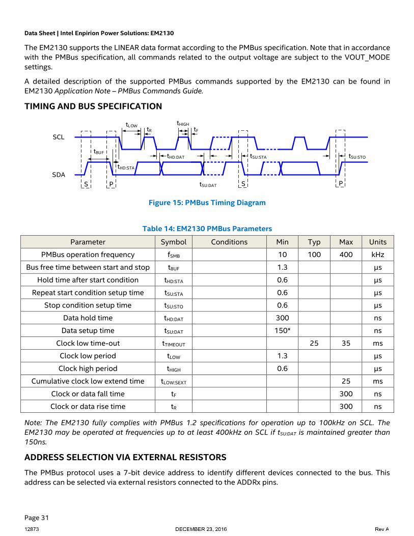
TIMING AND BUS SPECIFICATION
S P
tBUF
tHD:STA
tLOWtR
tHD:DAT
tHIGH
tF
tSU:DAT S P
tSU:STOtSU:STA
SCL
SDA
Figure 15: PMBus Timing Diagram
Table 14: EM2130 PMBus Parameters
Parameter Symbol Conditions Min Typ Max Units
PMBus operation frequency fSMB 10 100 400 kHz
Bus free time between start and stop tBUF 1.3 μs
Hold time after start condition tHD:STA 0.6 μs
Repeat start condition setup time tSU:STA 0.6 μs
Stop condition setup time tSU:STO 0.6 μs
Data hold time tHD:DAT 300 ns
Data setup time tSU:DAT 150* ns
Clock low time-out tTIMEOUT 25 35 ms
Clock low period tLOW 1.3 μs
Clock high period tHIGH 0.6 μs
Cumulative clock low extend time tLOW:SEXT 25 ms
Clock or data fall time tF 300 ns
Clock or data rise time tR 300 ns
Note: The EM2130 fully complies with PMBus 1.2 specifications for operation up to 100kHz on SCL. The
EM2130 may be operated at frequencies up to at least 400kHz on SCL if tSU:DAT is maintained greater than
150ns.
ADDRESS SELECTION VIA EXTERNAL RESISTORS
The PMBus protocol uses a 7-bit device address to identify different devices connected to the bus. This
address can be selected via external resistors connected to the ADDRx pins.

Data Sheet | Intel Enpirion Power Solutions: EM2130
Page 32
The resistor values are sensed using the internal ADC during the initialization phase and the appropriate
PMBus address is selected. Note that the respective circuitry is only active during the initialization phase;
hence no DC voltage can be measured at the pins. The supported PMBus addresses and the values of the
respective required resistors are listed in Table 16.
If only four devices are used in a system, their respective addresses can alternatively be configured without
resistors by connecting the pins to the AGND or VDD33 pin. The PMBus addresses selectable in this fashion
are listed in Table 15.
Table 15: PMBus Address Selection Without Resistors
Address ADDR1 ADDR0
0x0F GND VDD33
0x30 VDD33 GND
0x3F VDD33 VDD33
0x40 GND GND
Table 16: Supported Resistor Values For PMBus Address Selection
Address
(hex)
ADDR1
Ω
ADDR0
Ω
Address
(hex)
ADDR1
Ω
ADDR0
Ω
Address
(hex)
ADDR1
Ω
ADDR0
Ω
0x40 0 0 0x2B 1.2 k 12 k 0x56 3.9 k 4.7 k
0x01* 0 680 0x2C 1.2 k 15 k 0x57 3.9 k 5.6 k
0x02* 0 1.2 k 0x2D 1.2 k 18 k 0x58 3.9 k 6.8 k
0x03* 0 1.8 k 0x2E 1.2 k 22 k 0x59 3.9 k 8.2 k
0x04* 0 2.7 k 0x2F 1.2 k 27 k 0x5A 3.9 k 10 k
0x05* 0 3.9 k 0x30 1.8 k 0 0x5B 3.9 k 12 k
0x06* 0 4.7 k 0x31 1.8 k 680 0x5C 3.9 k 15 k
0x07* 0 5.6 k 0x32 1.8 k 1.2 k 0x5D 3.9 k 18 k
0x08* 0 6.8 k 0x33 1.8 k 1.8 k 0x5E 3.9 k 22 k
0x09 0 8.2 k 0x34 1.8 k 2.7 k 0x5F 3.9 k 27 k
0x0A 0 10 k 0x35 1.8 k 3.9 k 0x60 4.7 k 0
0x0B 0 12 k 0x36 1.8 k 4.7 k 0x61* 4.7 k 680
0x0C* 0 15 k 0x37* 1.8 k 5.6 k 0x62 4.7 k 1.2 k
0x0D 0 18 k 0x38 1.8 k 6.8 k 0x63 4.7 k 1.8 k
0x0E 0 22 k 0x39 1.8 k 8.2 k 0x64 4.7 k 2.7 k
0x0F 0 27 k 0x3A 1.8 k 10 k 0x65 4.7 k 3.9 k
0x10 680 0 0x3B 1.8 k 12 k 0x66 4.7 k 4.7 k
0x11 680 680 0x3C 1.8 k 15 k 0x67 4.7 k 5.6 k
0x12 680 1.2 k 0x3D 1.8 k 18 k 0x68 4.7 k 6.8 k
0x13 680 1.8 k 0x3E 1.8 k 22 k 0x69 4.7 k 8.2 k
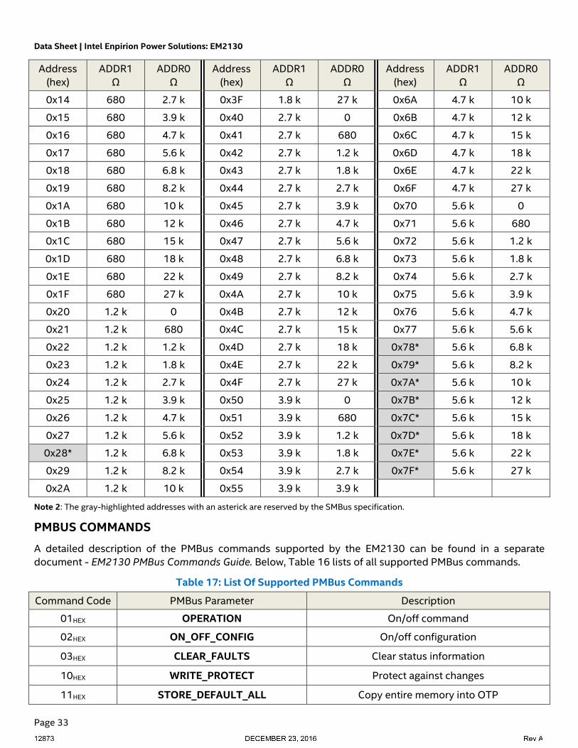
Data Sheet | Intel Enpirion Power Solutions: EM2130
Page 33
Address
(hex)
ADDR1
Ω
ADDR0
Ω
Address
(hex)
ADDR1
Ω
ADDR0
Ω
Address
(hex)
ADDR1
Ω
ADDR0
Ω
0x14 680 2.7 k 0x3F 1.8 k 27 k 0x6A 4.7 k 10 k
0x15 680 3.9 k 0x40 2.7 k 0 0x6B 4.7 k 12 k
0x16 680 4.7 k 0x41 2.7 k 680 0x6C 4.7 k 15 k
0x17 680 5.6 k 0x42 2.7 k 1.2 k 0x6D 4.7 k 18 k
0x18 680 6.8 k 0x43 2.7 k 1.8 k 0x6E 4.7 k 22 k
0x19 680 8.2 k 0x44 2.7 k 2.7 k 0x6F 4.7 k 27 k
0x1A 680 10 k 0x45 2.7 k 3.9 k 0x70 5.6 k 0
0x1B 680 12 k 0x46 2.7 k 4.7 k 0x71 5.6 k 680
0x1C 680 15 k 0x47 2.7 k 5.6 k 0x72 5.6 k 1.2 k
0x1D 680 18 k 0x48 2.7 k 6.8 k 0x73 5.6 k 1.8 k
0x1E 680 22 k 0x49 2.7 k 8.2 k 0x74 5.6 k 2.7 k
0x1F 680 27 k 0x4A 2.7 k 10 k 0x75 5.6 k 3.9 k
0x20 1.2 k 0 0x4B 2.7 k 12 k 0x76 5.6 k 4.7 k
0x21 1.2 k 680 0x4C 2.7 k 15 k 0x77 5.6 k 5.6 k
0x22 1.2 k 1.2 k 0x4D 2.7 k 18 k 0x78* 5.6 k 6.8 k
0x23 1.2 k 1.8 k 0x4E 2.7 k 22 k 0x79* 5.6 k 8.2 k
0x24 1.2 k 2.7 k 0x4F 2.7 k 27 k 0x7A* 5.6 k 10 k
0x25 1.2 k 3.9 k 0x50 3.9 k 0 0x7B* 5.6 k 12 k
0x26 1.2 k 4.7 k 0x51 3.9 k 680 0x7C* 5.6 k 15 k
0x27 1.2 k 5.6 k 0x52 3.9 k 1.2 k 0x7D* 5.6 k 18 k
0x28* 1.2 k 6.8 k 0x53 3.9 k 1.8 k 0x7E* 5.6 k 22 k
0x29 1.2 k 8.2 k 0x54 3.9 k 2.7 k 0x7F* 5.6 k 27 k
0x2A 1.2 k 10 k 0x55 3.9 k 3.9 k
Note 2: The gray-highlighted addresses with an asterick are reserved by the SMBus specification.
PMBUS COMMANDS
A detailed description of the PMBus commands supported by the EM2130 can be found in a separate
document - EM2130 PMBus Commands Guide. Below, Table 16 lists of all supported PMBus commands.
Table 17: List Of Supported PMBus Commands
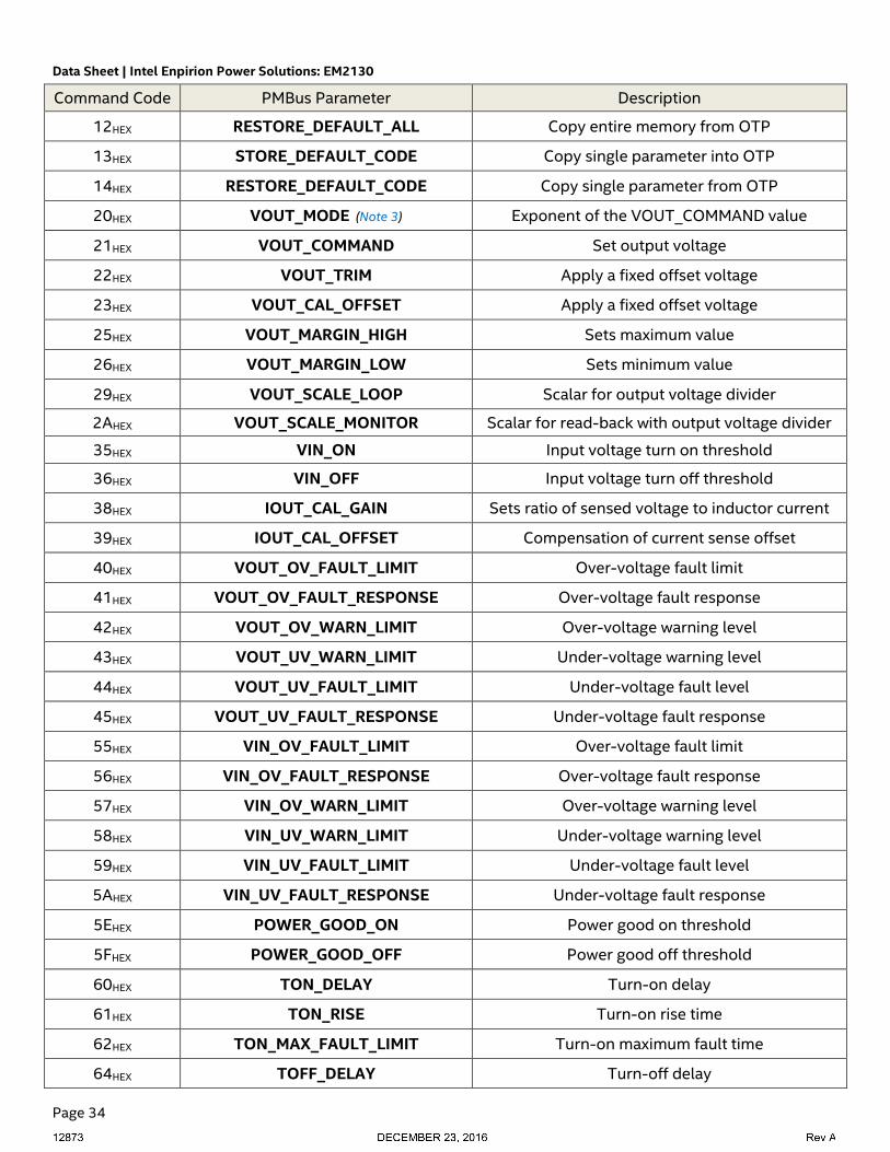
Command Code PMBus Parameter Description
01HEX OPERATION On/off command
02HEX ON_OFF_CONFIG On/off configuration
03HEX CLEAR_FAULTS Clear status information
10HEX WRITE_PROTECT Protect against changes
11HEX STORE_DEFAULT_ALL Copy entire memory into OTP
Data Sheet | Intel Enpirion Power Solutions: EM2130
Page 34
Command Code PMBus Parameter Description
12HEX RESTORE_DEFAULT_ALL Copy entire memory from OTP
13HEX STORE_DEFAULT_CODE Copy single parameter into OTP
14HEX RESTORE_DEFAULT_CODE Copy single parameter from OTP
20HEX VOUT_MODE (Note 3) Exponent of the VOUT_COMMAND value
21HEX VOUT_COMMAND Set output voltage
22HEX VOUT_TRIM Apply a fixed offset voltage
23HEX VOUT_CAL_OFFSET Apply a fixed offset voltage
25HEX VOUT_MARGIN_HIGH Sets maximum value
26HEX VOUT_MARGIN_LOW Sets minimum value
29HEX VOUT_SCALE_LOOP Scalar for output voltage divider
2AHEX VOUT_SCALE_MONITOR Scalar for read-back with output voltage divider
35HEX VIN_ON Input voltage turn on threshold
36HEX VIN_OFF Input voltage turn off threshold
38HEX IOUT_CAL_GAIN Sets ratio of sensed voltage to inductor current
39HEX IOUT_CAL_OFFSET Compensation of current sense offset
40HEX VOUT_OV_FAULT_LIMIT Over-voltage fault limit
41HEX VOUT_OV_FAULT_RESPONSE Over-voltage fault response
42HEX VOUT_OV_WARN_LIMIT Over-voltage warning level
43HEX VOUT_UV_WARN_LIMIT Under-voltage warning level
44HEX VOUT_UV_FAULT_LIMIT Under-voltage fault level
45HEX VOUT_UV_FAULT_RESPONSE Under-voltage fault response
55HEX VIN_OV_FAULT_LIMIT Over-voltage fault limit
56HEX VIN_OV_FAULT_RESPONSE Over-voltage fault response
57HEX VIN_OV_WARN_LIMIT Over-voltage warning level
58HEX VIN_UV_WARN_LIMIT Under-voltage warning level
59HEX VIN_UV_FAULT_LIMIT Under-voltage fault level
5AHEX VIN_UV_FAULT_RESPONSE Under-voltage fault response
5EHEX POWER_GOOD_ON Power good on threshold
5FHEX POWER_GOOD_OFF Power good off threshold
60HEX TON_DELAY Turn-on delay
61HEX TON_RISE Turn-on rise time
62HEX TON_MAX_FAULT_LIMIT Turn-on maximum fault time
64HEX TOFF_DELAY Turn-off delay
Data Sheet | Intel Enpirion Power Solutions: EM2130
Page 35
Command Code PMBus Parameter Description
65HEX TOFF_FALL Turn-off fall time
66HEX TOFF_MAX_WARN_LIMIT Turn-off maximum warning time
78HEX STATUS_BYTE Unit status byte
79HEX STATUS_WORD Unit status word
7AHEX STATUS_VOUT Output voltage status
7BHEX STATUS_IOUT Output current status
7CHEX STATUS_INPUT Input status
7EHEX STATUS_CML Communication and memory status
80HEX STATUS_MFR_SPECIFIC Manufacturer specific status
88HEX READ_VIN Reads input voltage
8BHEX READ_VOUT Reads output voltage
8CHEX READ_IOUT Reads output current
8EHEX READ_TEMPERATURE Reads temperature
95HEX READ_FREQUENCY Reads switching frequency
96HEX READ_POUT Reads output power
98HEX PMBUS™_REVISION PMBus™ revision
99HEX MFR_ID Manufacturer ID
9AHEX MFR_MODEL Manufacturer model identifier
9BHEX MFR_REVISION Manufacturer product revision
9EHEX MFR_SERIAL Serial number
A0HEX MFR_VIN_MIN Minimum input voltage
A4HEX MFR_VOUT_MIN Minimum output voltage
D0HEX MFR_SPECIFIC_00 Write word (once) / Read word – 2 bytes
D1HEX MFR_SPECIFIC_01 Write word / read word – 12 bytes
D2HEX MFR_READ_VCC Reads VCC voltage
D3HEX MFR_RESYNC Active RESYNC
DAHEX MFR_RTUNE_CONFIG Gets/sets RTUNE settings
DBHEX MFR_VOUT_MARGIN_HIGH Gets/sets Margin High
DCHEX MFR_VOUT_MARGIN_LOW Gets/sets Margin Low
DDHEX MFR_RTUNE_INDEX Returns index derived from resistor detected on
RTUNE pin
DEHEX MFR_RVSET_INDEX Returns index derived from resistor detected on
RVSET pin
Data Sheet | Intel Enpirion Power Solutions: EM2130
Page 36
Command Code PMBus Parameter Description
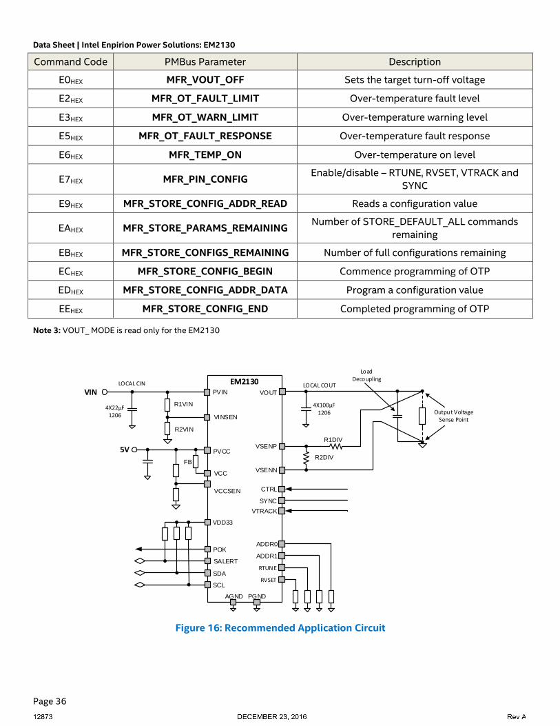
E0HEX MFR_VOUT_OFF Sets the target turn-off voltage
E2HEX MFR_OT_FAULT_LIMIT Over-temperature fault level
E3HEX MFR_OT_WARN_LIMIT Over-temperature warning level
E5HEX MFR_OT_FAULT_RESPONSE Over-temperature fault response
E6HEX MFR_TEMP_ON Over-temperature on level
E7HEX MFR_PIN_CONFIG Enable/disable – RTUNE, RVSET, VTRACK and
SYNC
E9HEX MFR_STORE_CONFIG_ADDR_READ Reads a configuration value
EAHEX MFR_STORE_PARAMS_REMAINING Number of STORE_DEFAULT_ALL commands
remaining
EBHEX MFR_STORE_CONFIGS_REMAINING Number of full configurations remaining
ECHEX MFR_STORE_CONFIG_BEGIN Commence programming of OTP
EDHEX MFR_STORE_CONFIG_ADDR_DATA Program a configuration value
EEHEX MFR_STORE_CONFIG_END Completed programming of OTP
Note 3: VOUT_ MODE is read only for the EM2130
Output Voltage Sense Point
PGND
EM2130
AGND
VINSEN
R1VIN
R2VIN
VIN PVIN
VSENP
VSENN
VOUT
R1DIV
R2DIV
LOCAL COUT
RVSET
RTUNE
ADDR0
ADDR1
VTRACK
VDD33
POK
SCL
SDA
SALERT
CTRL
SYNC
VCC
PVCC5V
LoadDecoupling
LOCAL CIN
4X22µF1206
4X100µF1206
FB
VCCSEN
Figure 16: Recommended Application Circuit
Data Sheet | Intel Enpirion Power Solutions: EM2130
Page 37
Layout Recommendations
Recommendation 1: It is highly recommended to use separate nets for AGND and PGND and connecting
them through a 0Ω resistor or a short. This method helps with ground management and prevents the noise
from the Power Ground disturbing the more sensitive Analog (“Signal”) Ground.
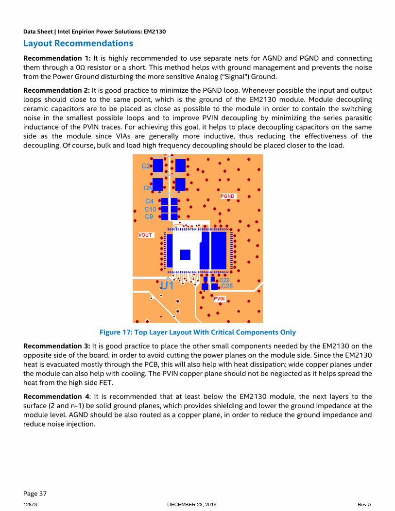
Recommendation 2: It is good practice to minimize the PGND loop. Whenever possible the input and output
loops should close to the same point, which is the ground of the EM2130 module. Module decoupling
ceramic capacitors are to be placed as close as possible to the module in order to contain the switching
noise in the smallest possible loops and to improve PVIN decoupling by minimizing the series parasitic
inductance of the PVIN traces. For achieving this goal, it helps to place decoupling capacitors on the same
side as the module since VIAs are generally more inductive, thus reducing the effectiveness of the
decoupling. Of course, bulk and load high frequency decoupling should be placed closer to the load.
Figure 17: Top Layer Layout With Critical Components Only
Recommendation 3: It is good practice to place the other small components needed by the EM2130 on the
opposite side of the board, in order to avoid cutting the power planes on the module side. Since the EM2130
heat is evacuated mostly through the PCB, this will also help with heat dissipation; wide copper planes under
the module can also help with cooling. The PVIN copper plane should not be neglected as it helps spread the
heat from the high side FET.
Recommendation 4: It is recommended that at least below the EM2130 module, the next layers to the
surface (2 and n-1) be solid ground planes, which provides shielding and lower the ground impedance at the
module level. AGND should be also routed as a copper plane, in order to reduce the ground impedance and
reduce noise injection.

Data Sheet | Intel Enpirion Power Solutions: EM2130
Page 38
Figure 18: VIAs in The Power Pads
Recommendation 5: In order to better spread the current and the heat through the inner layers, arrays of
VIAs should be placed in the power pads. 10mils diameter is a good size for the plated in-pad VIAs. It is
critical that through VIAs should not be placed by any means elsewhere under the module; the non-pad area
around AGND is VIA keep out area.
Recommendation 6: All other signal and LDO decoupling capacitors should be placed as close as possible to
the terminal they are decoupling, while the AGND connection should be done through VIAs to the AGND
plane.
Figure 19: Backside Decoupling
All Signal Decoupling Go To The Bottom AGND Plane And Get Connected To The EM2130 Module AGND
Through The AGND In-PAD VIAs (Again, No Other VIAs Are Allowed In That Area)
Recommendation 7: Figure 20 also shows the 0Ω resistor that connects AGND to PGND. The recommended
connecting point, as shown, is to a quiet PGND the output capacitors PGND.
Recommendation 8: Differential remote sense should be routed as much as possible as a differential pair, on
an inner layer, preferably shielded by a ground plane.

Data Sheet | Intel Enpirion Power Solutions: EM2130
Page 39
Figure 20: Remote Sense Routing On An Inner Layer (Highlighted, Yellow)
Recommendation 9: If the design allows it, stitching VIAs can be used on the power planes, close to the
module in order to help with cooling. This is a thermal consideration and does not matter much for the
electrical design.

Data Sheet | Intel Enpirion Power Solutions: EM2130
Page 40
Recommended PCB Footprint
Figure 21: Recommended PCB Footprint

Data Sheet | Intel Enpirion Power Solutions: EM2130
Page 41
Recommended Solder Stencil Aperture
Figure 22: Recommended Solder Stencil Aperture
Data Sheet | Intel Enpirion Power Solutions: EM2130
Page 42
Package Dimensions
Figure 23: Package Dimensions
Data Sheet | Intel Enpirion Power Solutions: EM2130
Page 43
Tray Information
Figure 24: Tray Information ½
Data Sheet | Intel Enpirion Power Solutions: EM2130
Page 44
Tray Information (Continued)
Figure 25: Tray Information 2/2

Data Sheet | Intel Enpirion Power Solutions: EM2130
Page 45
Revision History
Rev Date Change(s)
A 23-Dec-16 Initial Release

Data Sheet | Intel Enpirion Power Solutions: EM2130
Where to Get More Information
For more information about Intel and Intel Enpirion PowerSoCs, visit https://www.altera.com/enpirion
© 2016 Intel Corporation. All rights reserved. Intel, the Intel logo, Altera, ARRIA, CYCLONE, ENPIRION, MAX, MEGACORE, NIOS, QUARTUS, and STRATIX words and logos are trademarks of Intel
Corporation or its subsidiaries in the U.S. and/or other countries. Other marks and brands may be claimed as the property of others. Intel reserves the right to make changes to any products and
services at any time without notice. Intel assumes no responsibility or liability arising out of the application or use of any information, product, or service described herein except as expressly agreed to
in writing by Intel. Intel customers are advised to obtain the latest version of device specifications before relying on any published information and before placing orders for products or services.
* Other marks and brands may be claimed as the property of others.
Page 46


